WO2025023225A1 - 基板ユニット及び電子装置 - Google Patents
基板ユニット及び電子装置 Download PDFInfo
- Publication number
- WO2025023225A1 WO2025023225A1 PCT/JP2024/026227 JP2024026227W WO2025023225A1 WO 2025023225 A1 WO2025023225 A1 WO 2025023225A1 JP 2024026227 W JP2024026227 W JP 2024026227W WO 2025023225 A1 WO2025023225 A1 WO 2025023225A1
- Authority
- WO
- WIPO (PCT)
- Prior art keywords
- heat dissipation
- dissipation member
- substrate
- thermal conductivity
- graphite block
- Prior art date
- Legal status (The legal status is an assumption and is not a legal conclusion. Google has not performed a legal analysis and makes no representation as to the accuracy of the status listed.)
- Pending
Links
Images













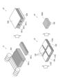
Classifications
-
- H—ELECTRICITY
- H01—ELECTRIC ELEMENTS
- H01S—DEVICES USING THE PROCESS OF LIGHT AMPLIFICATION BY STIMULATED EMISSION OF RADIATION [LASER] TO AMPLIFY OR GENERATE LIGHT; DEVICES USING STIMULATED EMISSION OF ELECTROMAGNETIC RADIATION IN WAVE RANGES OTHER THAN OPTICAL
- H01S5/00—Semiconductor lasers
- H01S5/02—Structural details or components not essential to laser action
- H01S5/024—Arrangements for thermal management
-
- H—ELECTRICITY
- H05—ELECTRIC TECHNIQUES NOT OTHERWISE PROVIDED FOR
- H05K—PRINTED CIRCUITS; CASINGS OR CONSTRUCTIONAL DETAILS OF ELECTRIC APPARATUS; MANUFACTURE OF ASSEMBLAGES OF ELECTRICAL COMPONENTS
- H05K7/00—Constructional details common to different types of electric apparatus
- H05K7/20—Modifications to facilitate cooling, ventilating, or heating
-
- H—ELECTRICITY
- H10—SEMICONDUCTOR DEVICES; ELECTRIC SOLID-STATE DEVICES NOT OTHERWISE PROVIDED FOR
- H10W—GENERIC PACKAGES, INTERCONNECTIONS, CONNECTORS OR OTHER CONSTRUCTIONAL DETAILS OF DEVICES COVERED BY CLASS H10
- H10W40/00—Arrangements for thermal protection or thermal control
- H10W40/10—Arrangements for heating
-
- H—ELECTRICITY
- H10—SEMICONDUCTOR DEVICES; ELECTRIC SOLID-STATE DEVICES NOT OTHERWISE PROVIDED FOR
- H10W—GENERIC PACKAGES, INTERCONNECTIONS, CONNECTORS OR OTHER CONSTRUCTIONAL DETAILS OF DEVICES COVERED BY CLASS H10
- H10W70/00—Package substrates; Interposers; Redistribution layers [RDL]
- H10W70/60—Insulating or insulated package substrates; Interposers; Redistribution layers
Definitions
- This disclosure relates to a board unit and an electronic device.
- Reference 1 shows a package for mounting optical elements.
- the substrate unit includes: A substrate; a heat dissipation member located on the substrate and including a carbon material; an element mounting portion located on the opposite side of the substrate with respect to the heat dissipation member; the element mounting portion and the substrate are thermally connected via the heat dissipation member, In the direction in which the substrate and the heat dissipation member are arranged, the heat dissipation member has a higher thermal conductivity than the substrate.
- the electronic device comprises: The above-mentioned board unit, an electronic element mounted on the element mounting portion; Equipped with.
- FIG. 2 is a plan view showing a substrate unit according to the first embodiment of the present disclosure.
- 1B is a diagram showing a substrate unit according to the first embodiment of the present disclosure, and is a cross-sectional view taken along line BB in FIG. 1A.
- FIG. 2 is a perspective view showing a heat dissipation member according to the first embodiment of the present disclosure.
- FIG. 2 is a perspective view showing the heat dissipation member according to the first embodiment of the present disclosure, showing the configuration excluding the protective layer.
- FIG. 2 is a perspective view showing the heat dissipation member according to the first embodiment of the present disclosure, excluding the protective layer, the first plate member, and the second plate member.
- 2B is a cross-sectional view taken along line AA in FIG.
- FIG. 2 is a diagram illustrating the properties of a graphite block.
- FIG. 2 is a cross-sectional view showing a first side of a graphite block.
- FIG. 4 is a cross-sectional view showing a second side of the graphite block.
- FIG. 13 is a diagram for explaining the thermal expansion characteristics of a sample, and is a characteristic diagram of a single graphite block.
- FIG. 13 is a diagram for explaining thermal expansion characteristics of a sample, and is a characteristic diagram of oxygen-free copper.
- FIG. 13 is a diagram for explaining the thermal expansion characteristics of a sample, and is a characteristic diagram of a configuration in which an oxygen-free copper plate is joined to a graphite block.
- FIG. 7B is a perspective view showing the sample of FIG.
- FIG. 7A is a perspective view showing the sample of FIG. 7B.
- FIG. 7D is a perspective view showing the sample of FIG. 7C.
- 1 is a cross-sectional view showing an electronic device incorporating a board unit.
- FIG. 13 is a perspective view showing a configuration in which the arrangement direction of element mounting portions is parallel to the direction in which the crystal planes of the graphite block extend, and shows the relationship between the heat dissipation member and the element mounting portions (submount substrate).
- FIG. 13 is a diagram showing a configuration in which the arrangement direction of element mounting portions is parallel to the direction in which crystal planes in the graphite block extend, and is a plan view showing the relationship between the graphite block and the element mounting portions.
- FIG. 13 is a perspective view showing a configuration in which the arrangement direction of element mounting portions is parallel to the direction in which crystal planes in the graphite block extend, and is a plan view showing the relationship between the graphite block and the element mounting portions.
- FIG. 13 is a perspective view showing a configuration in which the arrangement direction of the element mounting portions is perpendicular to the direction in which the crystal planes of the graphite block extend, and shows the relationship between the heat dissipation member and the element mounting portions (submount substrate).
- FIG. 13 is a diagram showing a configuration in which the arrangement direction of element mounting portions is perpendicular to the direction in which crystal planes in the graphite block extend, and is a plan view showing the relationship between the graphite block and the element mounting portions.
- FIG. 13 is a perspective view showing a configuration in which the arrangement direction of element mounting portions is inclined with respect to the direction in which the crystal planes of the graphite block extend, and shows the relationship between the heat dissipation member and the element mounting portions (submount substrate).
- FIG. 13 is a diagram showing a configuration in which the arrangement direction of element mounting portions is inclined with respect to the extending direction of the crystal plane of the graphite block, and is a plan view showing the relationship between the graphite block and the element mounting portions.
- FIG. 13 is a diagram showing a configuration in which the arrangement direction of the element mounting portions is inclined with respect to the extension direction of the crystal plane in the graphite block, and is a plan view for explaining the inclination angle, which is an angle at which the first heat transfer area and the second heat transfer area partially overlap, and an angle at which the first heat transfer area and the third heat transfer area do not overlap.
- FIG. 13 is a diagram showing a configuration in which the arrangement direction of element mounting portions is inclined with respect to the extension direction of the crystal plane in the graphite block, and is a plan view for explaining the inclination angle, which is an angle at which the first heat transfer area and the second heat transfer area partially overlap, and an angle at which the first heat transfer area and the third heat transfer area do not overlap.
- FIG. 13 is a diagram showing a configuration in which the arrangement direction of the element mounting parts is inclined with respect to the extension direction of the crystal plane of the graphite block, and is a plan view for explaining the inclination angle, which is an angle at which the first heat transfer region does not overlap with the second heat transfer region and the third heat transfer region.
- FIG. 11 is a perspective view showing a heat dissipation member according to a second embodiment of the present disclosure, showing a configuration excluding a protective layer.
- FIG. 11 is a perspective view showing a heat dissipation member according to a second embodiment of the present disclosure, excluding a protective layer, a first plate member, and a second plate member.
- FIG. 11 is a perspective view showing a heat dissipation member according to a third embodiment of the present disclosure, showing a configuration excluding a protective layer.
- FIG. 11 is a perspective view showing a heat dissipation member according to a third embodiment of the present disclosure, excluding a protective layer, a first plate member, and a second plate member.
- 1A to 1C are diagrams illustrating an example of a manufacturing method for a heat dissipation member according to the present disclosure.
- Electronic elements such as optical elements are heat sources, and therefore there is a demand for improved heat dissipation performance in the substrate units on which the electronic elements are mounted.
- the present disclosure aims to provide a board unit and an electronic device with improved heat dissipation performance.
- First Embodiment 1A and 1B are diagrams showing an example of a substrate unit 10 according to a first embodiment of the present disclosure, where FIG. 1A is a plan view and FIG. 1B is a cross-sectional view taken along line BB of FIG. 1A.
- the board unit 10 of the embodiment includes a board 20 on which an electronic element 310 ( FIG. 9 ) is mounted, and a heat dissipation member 100 that removes heat from the electronic element 310 .
- the substrate 20 may be made of metal. Specifically, a metal material such as copper or aluminum may be used for the substrate 20, or an alloy material containing copper or aluminum may be used for the substrate 20. This configuration allows the substrate unit 10 to be manufactured at a low cost.
- the substrate 20 may have a frame portion 21 on its upper surface.
- a recess for accommodating the electronic element 310 can be formed by the upper surface of the substrate 20 and the inner surface of the frame portion 21.
- the substrate unit 10 is provided with an electronic element accommodating package having a recess for accommodating the electronic element 310.
- the frame 21 may be made of the same material as the substrate 20 or may be made of a different material than the substrate 20 .
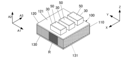
- the substrate unit 10 may further include a plurality of submount substrates 30 located in an area surrounded by the frame portion 21.
- the substrate unit 10 in one embodiment includes three submount substrates 30, but the number of submount substrates 30 included in the substrate unit 10 is not limited to three, and may be one, two, or four or more.
- the submount substrate 30 may be a circuit board.
- the material of the submount substrate 30 may be silicon nitride ceramics. This configuration can ensure insulation between the heat dissipation member 100 and the electronic element 310, and can impart high thermal conductivity characteristics to the submount substrate 30. Furthermore, this configuration can impart toughness to the submount substrate 30, making it easier to make the submount substrate 30 thinner. Moreover, the material of the submount substrate 30 may be alumina ceramics. This configuration can ensure insulation between the heat dissipation member 100 and the electronic element 310, and can impart high strength to the submount substrate 30. Therefore, it is easy to make the submount substrate 30 thinner. The material of the submount substrate 30 may be aluminum nitride ceramics. The submount substrate 30 may be made of a semiconductor material such as SiC (silicon carbide).
- the submount substrate 30 may be fixed to the heat dissipation member 100 via a third bonding material 40 located on the heat dissipation member 100.
- the submount substrate 30 may be bonded to the upper surface 101 of the heat dissipation member 100 via the third bonding material 40 located between the lower surface of the submount substrate 30 and the upper surface 101 of the heat dissipation member 100.
- Solder may be applied as the third bonding material 40. This configuration can reduce the inhibition of heat conduction caused by the third bonding material 40.
- the third bonding material 40 may be a thermally conductive adhesive, a thermally conductive filler (grease, etc.), or the like.
- the substrate unit 10 may further include an element mounting portion 50 located within the frame portion 21.
- the substrate unit 10 in one embodiment includes three element mounting portions 50, but the number of element mounting portions 50 included in the substrate unit 10 is not limited to three, and may be one, two, or four or more.
- the direction in which the multiple element mounting portions 50 are lined up is referred to as the X direction
- the direction in which the element mounting portions 50 extend is referred to as the Y direction
- a plane extending in the X and Y directions is referred to as the XY plane
- a direction intersecting (e.g., perpendicular to) the XY plane is referred to as the Z direction.
- the element mounting portion 50 has a dimension in the X direction that is shorter than the dimension in the Y direction, but is not limited to this, and the dimension in the X direction may be longer than the dimension in the Y direction, or the dimension in the X direction may be the same as the dimension in the Y direction.
- the shape of the element mounting portion 50 in a plan view may be larger than the shape of the electronic element 310 placed on the element mounting portion 50 in a plan view. Note that the shape of the element mounting portion 50 in a plan view may be the same as the shape of the electronic element 310 placed on the element mounting portion 50 in a plan view.
- the submount substrate 30 is a substrate that is interposed between the electronic element 310 and an object (substrate 20) to which the electronic element 310 is to be mounted, in order to mount the electronic element 310 on a module substrate, a package, etc. Therefore, at least a part of the upper surface of the submount substrate 30 may be the element mounting portion 50.
- the area surrounded by a two-dot chain line is an element mounting portion 50.
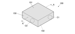
- FIGS. 2A, 2B, and 2C are diagrams showing an example of a heat dissipation member 100 according to the first embodiment of the present disclosure, in which Fig. 2A is a perspective view of the heat dissipation member 100, Fig. 2B is a perspective view showing a configuration excluding the protective layer 150, and Fig. 2C is a perspective view showing a configuration excluding the protective layer 150, the first plate material 120, and the second plate material 130.
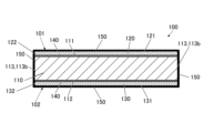
- Fig. 3 is a cross-sectional view taken along line A-A in Fig. 2A.
- Fig. 4 is a diagram for explaining the properties of the graphite block 110.
- the heat dissipation member 100 of one embodiment is a member that has high thermal conductivity and can quickly transfer heat received at the upper surface 101 to the lower surface 102.
- Heat dissipation member 100 may include a graphite block 110.
- Graphite block 110 may have a first surface 111, a second surface 112 located opposite first surface 111, and a side surface 113 located between first surface 111 and second surface 112.
- the heat dissipation member 100 may further include a second bonding material 140 located on the first surface 111 and the second surface 112, a first plate material 120 fixed to the first surface 111 via the second bonding material 140, a second plate material 130 fixed to the second surface 112 via the second bonding material 140, and a protective layer 150 covering the side surface 113.
- the graphite block 110 may have a structure in which a plurality of graphenes are stacked in the first direction A1.
- the graphene may be a sheet-like substance in which a honeycomb structure formed by bonding carbon atoms spreads in a two-dimensional direction. Adjacent graphenes may be bonded to each other by intermolecular forces, which are van der Waals forces.
- the surface of the graphite block 110 may have a surface on which graphene spreads in two dimensions and a surface on which multiple graphene layers appear.
- the surface on which graphene spreads in a two-dimensional direction is called a "crystal plane”
- the surface on which a graphene layer appears is called a “crystal layer plane.”
- the "crystal plane” is represented by a honeycomb pattern
- the “crystal layer plane” is represented by a striped pattern.
- Graphite block 110 may have anisotropy in its brittleness. As an example of anisotropy in its brittleness, graphite block 110 may have a tendency to cleave along a plane in which graphene extends, i.e., a plane that intersects with first direction A1, as shown in FIG. 4. Cleavage means to break along a certain plane. FIG. 4 shows a state in which crack E1 has occurred due to cleavage.
- the graphite block 110 may have a property that when stress is generated along the surface direction of the crystal plane, the graphene located on the crystal plane is easily peeled off. Furthermore, the graphite block 110 may have a property that the edge portion E2 of the graphene (see Figures 5 and 6) is weak and is easily broken from the edge portion E2.
- the graphite block 110 may be mainly composed of pyrolytic graphite, which may mean a volume ratio of 80% or more.
- Pyrolytic graphite may be produced as follows: First, a resin material such as polyimide is carbonized and decomposed into hydrocarbon gases. Next, the decomposed hydrocarbons are deposited and laminated. After that, a pressure annealing process is performed to produce pyrolytic graphite.
- the graphite block 110 may be of unitary construction.
- the first plate material 120 and the second plate material 130 may be bonded to the first surface 111 and the second surface 112 of the graphite block 110, respectively.
- the first surface 111 and the second surface 112 may be surfaces extending in the first direction A1.
- the first plate material 120 and the second plate material 130 are bonded to the crystal layer surfaces. Therefore, the first plate material 120 and the second plate material 130 can reduce the force applied to the graphite block 110 in a direction that causes it to cleave.
- the graphene on the crystal plane is likely to peel off due to stress generated during bonding.
- first plate material 120 and the second plate material 130 are bonded to the crystal plane, the graphene on the crystal plane is likely to peel off due to stress generated during bonding.
- first plate material 120 and the second plate material 130 are bonded to the crystal layer surface, the above-mentioned peeling of the graphene can be suppressed. Therefore, the toughness of the heat dissipation member 100 can be improved.
- FIG. 5 is a cross-sectional view showing the first side 113a of the graphite block 110.
- FIG. 6 is a cross-sectional view showing the second side 113b of the graphite block 110.
- FIG. 5 shows part C1 of FIG. 2A
- FIG. 6 shows part C2 of FIG. 2A.
- Side surface 113 of graphite block 110 may be a surface extending in a direction intersecting first direction A1.
- Side surface 113 may include first side surface 113a which is a crystal plane and second side surface 113b which is a crystal layer plane.
- the first side surface 113a which is a crystal plane, may be a plane extending in two directions intersecting the first direction A1.
- the two directions may be a second direction A2 and a third direction A3 that are perpendicular to the first direction A1 and perpendicular to each other.
- the second side surface 113b which is a crystal layer surface, may be a surface extending in the first direction A1 and the second direction A2.
- the protective layer 150 may cover the side surface 113.
- the first side surface 113a is a crystal plane where peeling of graphene is likely to occur, and edge portions E2 of the graphene that are likely to break may appear.
- the second side surface 113b is where edge portions E2 of the graphene that are likely to break appear.
- the graphite block 110 may be in the shape of a rectangular parallelepiped, with two opposing faces being crystal planes and the remaining four faces being crystal layer planes.
- the first surface 111 to which the first plate 120 is joined and the second surface 112 to which the second plate 130 is joined may be the crystal layer surface having the largest area among the four crystal layer surfaces and the crystal layer surface opposite to the largest area among the four crystal layer surfaces. This configuration can improve the stability of the mountability of the heat source (electronic element 310, etc.) to the heat dissipation member 100.
- a configuration may be adopted in which plate materials 120, 130 are positioned on two pairs of surfaces (i.e., four surfaces) of graphite block 110 via second bonding material 140.
- the remaining pair of surfaces i.e., two surfaces
- the two pairs of surfaces on which plate materials 120, 130 are positioned via second bonding material 140 may be crystal layer surfaces.
- the pair of surfaces covered by protective layer 150 may be crystal surfaces.
- Graphite block 110 may have very high thermal conductivity in a direction along a crystal plane.
- the thermal conductivity of graphite block 110 in second direction A2 and third direction A3 may be 200 W/m ⁇ K or more, while the thermal conductivity in first direction A1 may be a value lower than the thermal conductivity in second direction A2 or third direction A3, such as 7 W/m ⁇ K. That is, graphite block 110 may have anisotropy in thermal conductivity.
- the thermal conductivity in the second direction A2 and the third direction A3 may be preferably 370 W/m ⁇ K or more, more preferably 450 W/m ⁇ K or more, and even more preferably 800 W/m ⁇ K or more.
- the thermal conductivity in the second direction A2 and the third direction A3 of the graphite block 110 may be 1200 W/m ⁇ K or more, more specifically, about 1700 W/m ⁇ K.
- the thermal conductivity of the first plate material 120 and the second plate material 130 may be highly isotropic compared to that of the graphite block 110. Furthermore, the thermal conductivity of the first plate material 120 and the second plate material 130 may be higher than the thermal conductivity of the graphite block 110 in the first direction A1. According to this configuration, when heat is applied to a part of the first plate material 120 from the outside of the heat dissipation member 100, the heat is isotropically dispersed in the first plate material 120 and then transferred to the graphite block 110. Then, in the graphite block 110, the heat is quickly dispersed in the second direction A2 and the third direction A3, which have high thermal conductivity.
- the heat is conducted to the second plate material 130 and is isotropically dispersed in the second plate material 130.
- the heat can be dispersed over a wide range of the graphite block 110.
- a wide area of the second plate 130 is thermally connected to the substrate 20, heat can be dissipated from a wide area of the second plate 130. Therefore, efficient heat transfer performance of the heat dissipation member 100 can be achieved.
- the thermal conductivity of the protective layer 150 may be highly isotropic compared to the graphite block 110.
- the thermal conductivity of the protective layer 150 may be higher than the thermal conductivity of the graphite block 110 in the first direction A1. This configuration provides an effect of dispersing heat in the first direction A1 via the protective layer 150 at the second side surface 113b. Therefore, by adding this dispersion effect, a more efficient heat transfer performance of the heat dissipation member 100 can be achieved.
- the surface roughness of the first side surface 113a may be smaller than the surface roughness of the first surface 111, which is a crystal layer surface.
- the surface roughness of the first surface 111 may be 20 times or more, 10 times or more and less than 20 times, or 5 times or more and less than 10 times, of the surface roughness of the first side surface 113a.
- the surface roughness refers to the arithmetic mean roughness Ra defined in JIS (Japanese Industrial Standards) _B_0601:2001.
- the surface roughness can be measured after removing the protective layer 150 and the first plate material 120 from the heat dissipation member 100.
- the edge portion E2 of the graphene appearing on the first side 113a is reduced. Therefore, the fragility of the first side 113a can be reduced. Furthermore, the small surface roughness reduces the adhesion between the protective layer 150 and the first side 113a. The low adhesion reduces the stress applied to the second side 113b when the protective layer 150 is formed. Therefore, it is possible to prevent a portion of the graphene from peeling off from the graphite block 110 on the second side 113b.
- the surface roughness of the second side surface 113b may be greater than the surface roughness of the first side surface 113a.
- the surface roughness of the second side surface 113b may be 20 times or more, 10 times or more but less than 20 times, or 5 times or more but less than 10 times, of the surface roughness of the first side surface 113a.
- the surface roughness refers to the arithmetic mean roughness Ra described above. The above surface roughness can be measured after removing the protective layer 150 from the heat dissipation member 100.
- second side 113b includes relatively large irregularities due to the surface roughness.
- the irregularities may be fine irregularities.
- a portion of protective layer 150 is located within recess F1 of the irregularities of second side 113b. Therefore, an anchor effect is produced, improving the adhesion of protective layer 150 to second side 113b. Therefore, peeling of protective layer 150 from graphite block 110 can be suppressed.
- the thermal resistance between protective layer 150 and graphite block 110 can be reduced compared to a configuration in which a gap occurs in recess F1.
- the linear expansion coefficient of graphite block 110 may be highly anisotropic on first surface 111 and second surface 112. Specifically, the linear expansion coefficient of graphite block 110 may be 20 [10 ⁇ -6/K] or more in first direction A1 and 0.050 [10 ⁇ -6/K] or less in second direction A2 and third direction A3. Furthermore, the linear expansion coefficient of graphite block 110 may be 24 [10 ⁇ -6/K] or more in first direction A1, and may be a value in the range of 27 [10 ⁇ -6/K] or less in first direction A1.
- the linear expansion coefficient of graphite block 110 in second direction A2 and third direction A3 may be a negative value, specifically, may be ⁇ 0.001 [10 ⁇ -6/K] or less.
- the linear expansion coefficient of graphite block 110 in second direction A2 and third direction A3 may be ⁇ 1.0 [10 ⁇ -6/K] or more.
- the linear expansion coefficient of the first plate material 120 may be highly isotropic compared to that of the graphite block 110.
- first direction A1 the linear expansion coefficient of the first plate material 120 may be smaller than that of the graphite block 110.
- second direction A2 the linear expansion coefficient of the first plate material 120 may be larger than that of the graphite block 110.
- third direction A3 the linear expansion coefficient of the first plate material 120 may be larger than that of the graphite block 110. The same applies to the second plate material 130.
- the linear expansion coefficient of the first plate material 120 and the second plate material 130 may be, for example, 4.0 [10 ⁇ -6/K] or more and less than 20 [10 ⁇ -6/K], and may further be 6.0 [10 ⁇ -6/K] or more and less than 18 [10 ⁇ -6/K].
- the first plate material 120 and the second plate material 130 may be made of a material having a linear expansion coefficient of 4.0 [10 ⁇ -6/K] or more and less than 20 [10 ⁇ -6/K], for example, a metal material such as copper or stainless steel, or a ceramic material such as aluminum nitride, alumina, or zirconia.
- a metal material having a linear expansion coefficient larger than that of copper, such as aluminum, may be used as the material of the first plate material 120 and the second plate material 130.
- the linear expansion coefficients of the first plate material 120 and the second plate material 130 are compared with that of the graphite block 110 using the linear expansion coefficients measured by changing the temperature from 20°C to 100°C.
- the linear expansion coefficients are measured using a measurement method specified in JIS according to the material. For example, if the first plate material 120 and the second plate material 130 are made of a metal material, the measurement method specified in JIS Z 2285:2003 is used. If the first plate material 120 and the second plate material 130 are made of a ceramic material, the measurement method specified in JIS R 1618:2002 is used.
- the linear expansion coefficient of the graphite block 110 is measured using the measurement method specified in JIS R 1618:2002.
- the above configuration allows the linear expansion coefficient of the upper surface 101 of the heat dissipation member 100 to approach an isotropic value, compared to a configuration using only the graphite block 110. Therefore, when mounting components on the upper surface 101 of the heat dissipation member 100, the reliability of the mounting can be improved. The same applies to the lower surface 102 of the heat dissipation member 100.
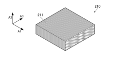
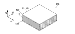
- FIG. 7A, Fig. 7B, and Fig. 7C are diagrams for explaining the thermal expansion characteristics of three samples
- Fig. 7A is a characteristic diagram of a graphite block alone
- Fig. 7B is a characteristic diagram of oxygen-free copper
- Fig. 7C is a characteristic diagram of a configuration in which an oxygen-free copper plate is joined to a graphite block.
- Fig. 8A, Fig. 8B, and Fig. 8C are perspective views showing the samples of Fig. 7A, Fig. 7B, and Fig. 7C, respectively.
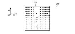
- the first sample 210 is a single graphite block made of pyrolytic graphite.
- the first sample 210 corresponds to the single graphite block 110 of the first embodiment.
- the upper surface 211 of the first sample 210 corresponds to the first surface 111 of the graphite block 110 of the first embodiment.
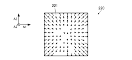
- the second sample 220 is an oxygen-free copper plate.
- the third sample 230 is a member in which a first plate material 120 and a second plate material 130, which are oxygen-free copper, are joined to a first surface 111 and a second surface 112 of a graphite block 110, which is pyrolytic graphite, with a brazing material.
- An upper surface 231 of the third sample 230 corresponds to an upper surface 121 of the first plate material 120.
- FIGS. 7A, 7B, and 7C are vector distribution diagrams showing the thermal expansion characteristics of the upper surfaces 211, 221, and 231 of the three samples 210, 220, and 230, respectively.
- the vectors in Figures 7A, 7B, and 7C were obtained as follows. First, digital images of each top surface 211, 221, and 231 were obtained at two different temperatures for each sample. The digital images were obtained using a CCD (Charge Coupled Device) camera. The two different temperatures were a standard temperature (e.g., 23°C) and a 100°C state. The temperature was adjusted by heaters arranged above and below the samples 210, 220, and 230.
- CCD Charge Coupled Device
- the linear expansion coefficient of the first sample 210 i.e., the graphite block alone, was highly anisotropic.
- the linear expansion coefficient of typical pyrolytic graphite in the first direction A1 was 25 [10 ⁇ -6/K], and the linear expansion coefficients in the second direction A2 and third direction A3 were -0.6 [10 ⁇ -6/K].
- the linear expansion coefficient of the second sample 220 i.e., oxygen-free copper
- the linear expansion coefficient of the first sample 210 (graphite block alone) in the first direction A1 was larger than the linear expansion coefficient of the second sample 220 (oxygen-free copper) in the first direction A1.
- the linear expansion coefficient of the first sample 210 (graphite block alone) in the third direction A3 was smaller than the linear expansion coefficient of the second sample 220 (oxygen-free copper) in the third direction A3.
- the linear expansion coefficient of the second sample 220 (oxygen-free copper) was 17.7 [10 ⁇ -6/K].
- the linear expansion coefficient of the third sample 230 i.e., the configuration in which the first and second oxygen-free copper plates 120 and 130 are joined to the graphite block 110, was anisotropic. However, the linear expansion coefficient was closer to a high isotropic value than that of the first sample 210 (graphite block alone). As shown by comparing FIG. 7A and FIG. 7C, the difference between the linear expansion coefficient of the third sample 230 in the first direction A1 and the linear expansion coefficient in the third direction A3 was smaller than the difference between the linear expansion coefficient of the first sample 210 in the first direction A1 and the linear expansion coefficient in the third direction A3. This characteristic was obtained by suppressing the anisotropy of the graphite block 110 with the isotropy of the linear expansion coefficient of the first and second plates 120 and 130.
- Heat dissipation member 100 of one embodiment has highly anisotropic graphite block 110.
- the linear expansion coefficients of upper surface 121 and lower surface 131 can be made closer to isotropic values.
- the mounting surface also has a linear expansion coefficient close to isotropic. This is because if the thermal expansion characteristics of the mounting surface are highly anisotropic, stress anisotropy occurs at the joint between the mounting surface and the component, and the component and mounting surface are likely to warp due to temperature changes. Alternatively, stress is difficult to disperse smoothly, and points where stress is concentrated are likely to occur.
- the coefficient of linear expansion of the upper surface 101 of the heat dissipation member 100 is closer to an isotropic value than that of the graphite block 110 alone. Therefore, when mounting components on the upper surface 101 of the heat dissipation member 100, the occurrence of warping due to temperature changes can be suppressed, and mounting can be achieved with reduced stress concentration. This improves the reliability of the mounting.
- the material of the first plate material 120 may be a copper-based metal or alloy such as oxygen-free copper. With this configuration, as shown in Fig. 7C, the anisotropy of the linear expansion coefficient on the upper surface 121 can be reduced. Furthermore, a high thermal conductivity of the first plate material 120 can be obtained, and the heat dissipation member 100 can achieve more efficient heat transfer performance.
- the first plate material 120 may be a metal with high thermal conductivity such as aluminum. In this configuration, the anisotropy of thermal expansion characteristics can be reduced as in the case of copper. Furthermore, the high thermal conductivity allows the heat dissipation member 100 to achieve efficient heat transfer performance. From the viewpoint of heat transfer, copper has better characteristics than aluminum.
- the first plate material 120 may be ceramics such as alumina ceramics, silicon nitride ceramics, and aluminum nitride ceramics. In this configuration, the anisotropy of the thermal expansion characteristics can be reduced, as in the case of copper. Furthermore, by using ceramics, when the heat dissipation member 100 is required to have insulating properties, the requirement can be met. When ceramics are used, the material of the first plate member 120 may be alumina ceramics or silicon nitride ceramics, which provides high rigidity against the residual stress of the graphite block 110. Furthermore, the material of the first plate member 120 may be aluminum nitride ceramics. By using this material, it is possible to impart high thermal conductivity characteristics in addition to rigidity to the first plate member 120, and it is possible to realize more efficient heat transfer performance of the heat dissipation member 100.
- ceramics such as alumina ceramics, silicon nitride ceramics, and aluminum nitride ceramics.
- the above-mentioned materials for the first plate material 120 can also be applied to the second plate material 130.
- the second plate material 130 also has the same effect as when the above-mentioned materials are applied to the first plate material 120.
- the hardness of the first plate material 120 and the second plate material 130 may be higher than the hardness of the graphite block 110. With this configuration, even if an external force is applied to the first plate material 120 and the second plate material 130, the external force is dispersed and acts on the graphite block 110. Therefore, it is possible to prevent the graphite block 110 from being damaged inside the first plate material 120 and the second plate material 130.
- the hardness of the graphite block 110 may be a Vickers hardness of 10 MPa or more and 40 MPa or less.
- the hardness of the first plate material 120 and the second plate material 130 may be preferably 10 times or more, more preferably 20 times or more, that of the graphite block 110.
- the hardness of the first plate material 120 and the second plate material 130 may be preferably a Vickers hardness of 200 MPa or more, more preferably a Vickers hardness of 500 MPa or more, and even more preferably a Vickers hardness of 900 MPa or more.
- the Vickers hardness of the first plate material 120 and the second plate material 130 can be measured using the measurement method specified in JIS Z 2244: 2009.
- the Vickers hardness of the graphite block 110 is a value converted from the measurement results using a nanoindentation test with a load of 20 mN/10 seconds.
- Examples of materials having a hardness 10 times or more that of graphite block 110 include various metal materials such as copper, aluminum, and stainless steel, and ceramic materials such as aluminum nitride, alumina, and zirconia.
- materials having a hardness 10 times or more that of graphite block 110 are not limited to metal materials and ceramic materials, and various materials such as resin materials may be used.
- the Vickers hardness is shown as a value obtained by converting the unit HV into pressure.
- the first plate material 120 may be joined to the first surface 111 via a second bonding material 140.
- the second plate material 130 may be joined to the second surface 112 via a second bonding material 140.
- a brazing material may be used for the second bonding material 140.
- the second bonding material 140 may be configured to cover the bonding surfaces of the first plate material 120 and the second plate material 130 (i.e., clad) during the manufacturing stage of the heat dissipation member 100. With this configuration, the bonding material after bonding can be made thinner. Therefore, the thermal resistance of the second bonding material 140 can be reduced.
- the second bonding material 140 may be configured to be formed in a sheet shape during the manufacturing process of the heat dissipation member 100.
- the sheet-shaped second bonding material 140 may be configured to exert a brazing effect by being sandwiched between the first plate material 120 and the graphite block 110 and then being subjected to a heating process and a cooling process.
- first surface 111 and second surface 112 of graphite block 110 have a large area, it is possible to improve the adhesion between first plate material 120 and graphite block 110 via second bonding material 140.
- By improving the adhesion it is possible to lower the thermal resistance between first plate material 120 and graphite block 110 and the thermal resistance between second plate material 130 and graphite block 110, as compared to a configuration in which a gap is present.
- the second bonding material 140 may be called an intervening layer.
- the second bonding material 140 may be located only in a portion of the first surface 111 and only in a portion of the second surface 112.
- the area of the first surface 111 other than the area where the second bonding material 140 is located may be filled with thermally conductive grease or the like as an intervening layer.
- the second bonding material 140 is located only in a portion of the second surface 112
- the area of the second surface 112 other than the area where the second bonding material 140 is located may be filled with thermally conductive grease or the like as an intervening layer.
- the protective layer 150 may be a plating layer or a resin film. By adopting a plating layer, the protective layer 150 having high thermal conductivity can be realized, which contributes to efficient heat transfer performance of the heat dissipation member 100. Furthermore, when the heat dissipation member 100 is required to have electrical conductivity, this requirement can be met. Furthermore, when an insulator such as ceramics is used for the first plate material 120 and the second plate material 130, a metal layer may be formed on the insulator, and a plating layer may be formed as the protective layer 150.
- the protective layer 150 may cover the side surface 122 of the first plate material 120 (see FIG. 2B and FIG. 3) and the side surface 132 of the second plate material 130 (see FIG. 2B and FIG. 3).
- the edges of the protective layer 150 are more likely to peel off than other parts.
- the side surface 122 of the first plate material 120 and the side surface 132 of the second plate material 130 are more likely to adhere the protective layer 150 with higher strength than the side surface 113 of the graphite block 110.
- the protective layer 150 covering a part of the first plate material 120 and the second plate material 130, the edge portion of the protective layer 150 is located on the surface of the first plate material 120 and the second plate material 130, and peeling of the protective layer 150 can be suppressed. Furthermore, the protective layer 150 is continuous from the surface of the first plate material 120 and the second plate material 130 to the side surface 113 of the graphite block 110. Therefore, peeling of the protective layer 150 can be suppressed, including the area of the side surface 113 of the graphite block 110.
- the protective layer 150 may further cover a portion of the upper surface 121 of the first plate material 120.
- the protective layer 150 may further cover a portion of the lower surface 131 of the second plate material 130.
- the upper surface 121 of the first plate material 120 is the surface opposite to the surface facing the graphite block 110.
- the lower surface 131 of the second plate material 130 is the surface opposite to the surface facing the graphite block 110. Even with this configuration, peeling of the protective layer 150 can be suppressed as described above.
- the upper surface 101 of the heat dissipation member 100 may correspond to the surface of the protective layer 150.
- the upper surface 101 of the heat dissipation member 100 may correspond to the upper surface 121 of the first plate 120.
- the protective layer 150 covers the lower surface 131 of the second plate 130, the lower surface 102 of the heat dissipation member 100 may correspond to the surface of the protective layer 150.
- the protective layer 150 does not cover the lower surface 131 of the second plate 130, the lower surface 102 of the heat dissipation member 100 may correspond to the lower surface 131 of the second plate 130.
- the protective layer 150 may further cover all of the side surfaces 122 and top surface 121 of the first plate material 120, all of the side surfaces 113 of the graphite block 110, and all of the side surfaces 132 and bottom surface 131 of the second plate material 130.
- Figures 2A and 3 show this configuration. With the above configuration, the edges of the protective layer 150 are reduced (e.g., eliminated), so peeling and damage of the protective layer 150 can be further suppressed. Furthermore, with this configuration, the complexity of the process of forming the protective layer 150 can be reduced.
- a material with high thermal conductivity such as a metal plating layer may be applied to the protective layer 150.
- a heat source such as an electronic element 310
- the heat dissipation member 100 may be fixed to the substrate 20 via a first bonding material 60 located on the substrate 20. That is, the heat dissipation member 100 may be bonded to the upper surface of the substrate 20 via the first bonding material 60 located between a lower surface 102 of the heat dissipation member 100 and the upper surface of the substrate 20. Solder may be applied to the first bonding material 60. This configuration can reduce the inhibition of heat conduction caused by the first bonding material 60.
- the first bonding material 60 may be a thermally conductive adhesive, a thermally conductive filler (grease, etc.), or the like.
- the substrate unit 10 may include a substrate 20, a heat dissipation member 100 that is located on the substrate 20 and contains a carbon material, and an element mounting portion 50 that is located on the opposite side of the substrate 20 with respect to the heat dissipation member 100.
- the element mounting portion 50 and the substrate 20 may be thermally connected via the heat dissipation member 100.
- the thermal conductivity of the heat dissipation member 100 may be higher than the thermal conductivity of the substrate 20 in the arrangement direction of the substrate 20 and the heat dissipation member 100 (Z direction, second direction A2).
- a heat dissipation member 100 having high thermal conductivity in the Z direction is arranged in the middle of the heat transfer path (heat transfer path parallel to the Z direction) from the element mounting portion 50 to the substrate 20, so that heat can be moved more quickly from the electronic element 310, which serves as a heat source, compared to a case in which the heat dissipation member 100 is not arranged between the substrate 20 and the element mounting portion 50.
- the substrate unit 10 may have an element mounting portion 50 on the first surface 111 of the heat dissipation member 100 (i.e., above the first surface 111 when the second surface 112 faces downward and the first surface 111 faces upward). That is, the heat dissipation member 100 may be bonded to the upper surface of the substrate 20 via a first bonding material 60 with the second surface 112 facing downward and the first surface 111 facing upward, and a submount substrate 30 may be bonded to the upper surface 101 via a third bonding material 40.
- the element mounting portion 50 may be a part of the upper surface 101 of the heat dissipation member 100. That is, the substrate unit 10 may not be provided with a submount substrate 30.
- the substrate unit 10 may have an element mounting portion 50 on the second surface 112 of the heat dissipation member 100 (i.e., above the second surface 112 when the first surface 111 faces downward and the second surface 112 faces upward).
- the element mounting portion 50 may be a part of the lower surface 102 of the heat dissipation member 100.
- the heat dissipation member 100 may include a graphite block 110 having anisotropic thermal conductivity, and a protective portion (first plate material 120, second plate material 130, protective layer 150) that covers the graphite block 110.
- a protective portion first plate material 120, second plate material 130, protective layer 150
- the board 20 may be made of metal. With this configuration, the graphite block 110 is placed on the metal board 20 (the bottom of the metal package), so that deformation of the board 20 can be prevented.
- the board when the board is made of a graphite block, heat can be quickly transferred from the electronic element 310, which is a heat source, even if the heat dissipation member 100 is not placed between the board (graphite block) and the element mounting portion 50.
- the board 20 may be made of ceramics.
- the thermal conductivity of the graphite block 110 in the alignment direction (Z direction, second direction A2) of the substrate 20 and the heat dissipation member 100 may be higher than the thermal conductivity of the graphite block 110 in a direction (first direction A1) that intersects (e.g., perpendicular to) the alignment direction. Furthermore, in the alignment direction (Z direction, second direction A2), the thermal conductivity of the heat dissipation member 100 may be higher than the thermal conductivity of the protective portion (first plate material 120, second plate material 130, protective layer 150).
- the thermal conductivity of the substrate 20 may be higher than the thermal conductivity of the heat dissipation member 100
- the thermal conductivity of the protective portion may be higher than the thermal conductivity of the heat dissipation member 100.
- the substrate 20 and the protective portion act to disperse heat in the one direction (first direction A1), thereby reducing the anisotropy of thermal conduction in the graphite block 110.
- the protective portion for protecting graphite block 110 may be plating alone. In other words, first surface 111, second surface 112, and side surface 113 of graphite block 110 may be covered with plating without providing first plate member 120 and second plate member 130. Further, the protective portion that protects the graphite block 110 may be made of an organic material or a ceramic material.
- the thermal conductivity of the first bonding material 60 bonding the substrate 20 and the heat dissipation member 100 may be higher than the thermal conductivity of the graphite block 110.
- the thermal conductivity of the second bonding material 140 bonding the graphite block 110 and the protective portion may be higher than the thermal conductivity of the graphite block 110.
- the inhibition of thermal conduction by the second bonding material 140 can be reduced compared to when the thermal conductivity of the second bonding material 140 is lower than the thermal conductivity of the graphite block 110 in the one direction (first direction A1).
- the melting point of the first bonding material 60 that bonds the substrate 20 and the heat dissipation member 100 may be lower than the melting point of the second bonding material 140 that bonds the graphite block 110 and the protective portion (first plate material 120, second plate material 130). According to this configuration, temperature control during mounting of the heat dissipation member 100 becomes easier than when the melting point of the first bonding material 60 is higher than the melting point of the second bonding material 140.
- the second bonding material 140 may melt and the bonding between the graphite block 110 and the protective portion (first plate material 120, second plate material 130) may be released, so temperature control is required to avoid melting of the second bonding material 140.
- the first bonding material 60 may be a bonding material with a relatively low melting point, such as a solder material.
- the second bonding material 140 may be a bonding material with a relatively high melting point, such as a metallic brazing material (for example, a copper brazing material).
- the melting point of the first bonding material 60 that bonds the substrate 20 and the heat dissipation member 100 may be lower than the melting point of the bonding material included in the package (for example, the bonding material that bonds the substrate 20 and the frame portion 21). According to this configuration, temperature control during mounting of the heat dissipation member 100 is easier than when the melting point of the first bonding material 60 is higher than the melting point of the bonding material included in the package.
- the first bonding material 60 may be a bonding material with a relatively low melting point, such as a solder material.
- the bonding material contained in the package may be a bonding material with a relatively high melting point, such as a metallic brazing material (eg, a copper brazing material).
- the element mounting portion 50 may be located on the heat dissipation member 100 via a submount substrate 30 including an insulating material. According to this configuration, the insulation between the heat dissipation member 100 and the electronic element 310 can be ensured.
- 1A and 1B includes a submount substrate 30, the substrate unit 10 does not necessarily have to include the submount substrate 30. In the case of this configuration, the submount substrate 30 and the electronic element 310 may be mounted on the substrate unit 10 when the electronic device 300 is manufactured.
- the melting point of the third bonding material 40 that bonds the heat dissipation member 100 and the submount substrate 30 may be lower than the melting point of the second bonding material 140 that bonds the graphite block 110 and the protective portion (first plate material 120, second plate material 130). According to this configuration, temperature control during mounting of the submount substrate 30 is easier than when the melting point of the third bonding material 40 is higher than that of the second bonding material 140.
- the third bonding material 40 may be a bonding material with a relatively low melting point, such as a solder material.
- the second bonding material 140 may be a bonding material with a relatively high melting point, such as a metallic brazing material (for example, a copper brazing material).
- the melting point of the third bonding material 40 that bonds the heat dissipation member 100 and the submount substrate 30 may be lower than the melting point of the bonding material included in the package (e.g., the bonding material that bonds the substrate 20 and the frame portion 21). According to this configuration, temperature control during mounting of the submount substrate 30 becomes easier than when the melting point of the third bonding material 40 is higher than the melting point of the bonding material included in the package.
- the third bonding material 40 may be a bonding material with a relatively low melting point, such as a solder material.
- the bonding material contained in the package may be a bonding material with a relatively high melting point, such as a metallic brazing material (eg, a copper brazing material).
- the melting point of the third bonding material 40 that bonds the heat dissipation member 100 and the submount substrate 30 may be lower than the melting point of the first bonding material 60 that bonds the substrate 20 and the heat dissipation member 100. According to this configuration, temperature control during mounting of the submount substrate 30 is easier than when the melting point of the third bonding material 40 is higher than the melting point of the first bonding material 60.
- the melting point of the third bonding material 40 is higher than the melting point of the first bonding material 60, there is a possibility that the first bonding material 60 melts and the bonding between the substrate 20 and the heat dissipation member 100 is released when the submount substrate 30 is fixed to the heat dissipation member 100 by the third bonding material 40, and therefore temperature control is required to avoid melting of the first bonding material 60.
- the melting point of the third bonding material 40 may be the same as the melting point of the first bonding material 60.
- the first bonding material 60 is a solder material having a different melting point before and after bonding (specifically, a solder material having a higher melting point after bonding than before bonding), such as a gold-based solder material, even if the melting point of the third bonding material 40 is the same as the melting point of the first bonding material 60 (the melting point before bonding), when the third bonding material 40 is used (when the submount substrate 30 is mounted), the melting point of the first bonding material 60 is higher than the melting point of the third bonding material 40, and therefore temperature management for avoiding melting of the first bonding material 60 is not required.
- a solder material having a different melting point before and after bonding specifically, a solder material having a higher melting point after bonding than before bonding
- a gold-based solder material even if the melting point of the third bonding material 40 is the same as the melting point of the first bonding material 60 (the melting point before bonding), when the third bonding material 40 is used (when the submount substrate 30 is
- the thermal conductivity of the heat dissipation member 100 may be higher than the thermal conductivity of the submount substrate 30. Furthermore, the thermal conductivity of the heat dissipation member 100 in the first direction A1 (the stacking direction of graphene) may be lower than the thermal conductivity of the submount substrate 30 in the X direction and the Y direction. Furthermore, the thermal conductivity of the submount substrate 30 may be highly isotropic compared to that of the graphite block 110 .
- the thermal conductivity of the heat dissipation member 100 may be higher than the thermal conductivity of the substrate 20. Furthermore, the thermal conductivity of the heat dissipation member 100 in the first direction A1 (the stacking direction of graphene) may be lower than the thermal conductivity of the substrate 20 in the X direction and the Y direction. Additionally, the thermal conductivity of the substrate 20 may be highly isotropic compared to that of the graphite block 110 .
- an electronic device 300 includes a board unit 10 and an electronic element 310 located on an element mounting portion 50 of the board unit 10.
- the electronic element 310 may be mounted on the element mounting portion 50 via a bonding material 320 such as solder. With this configuration, heat from the electronic element 310 can be rapidly conducted to the board 20 via the heat dissipation member 100.
- the melting point of the third bonding material 40 that bonds the heat dissipation member 100 and the submount substrate 30 may be lower than the melting point of the bonding material 320 that bonds the electronic element 310 and the submount substrate 30. According to this configuration, temperature control during mounting of the submount substrate 30 is easier than when the melting point of the third bonding material 40 is higher than the melting point of the bonding material 320.
- the melting point of the third bonding material 40 when the melting point of the third bonding material 40 is higher than the melting point of the bonding material 320, when the submount substrate 30 (the submount substrate 30 with the electronic element 310 fixed thereto) is fixed to the heat dissipation member 100 by the third bonding material 40, the bonding material 320 may melt and the bonding between the submount substrate 30 and the electronic element 310 may be released. Therefore, temperature control is required to avoid melting of the bonding material 320.
- the melting point of the third bonding material 40 may be the same as the melting point of the bonding material 320.
- the bonding material 320 is a solder material whose melting point differs before and after bonding, such as a gold-based solder material (specifically, a solder material whose melting point is higher after bonding than before bonding due to a change in the alloy state before and after bonding), even if the melting point of the third bonding material 40 is the same as the melting point of the bonding material 320 (the melting point before bonding), when the third bonding material 40 is used (when the submount substrate 30 is mounted), the melting point of the bonding material 320 is higher than the melting point of the third bonding material 40, so that temperature management to avoid melting of the bonding material 320 is not required.
- a solder material whose melting point differs before and after bonding such as a gold-based solder material (specifically, a solder material whose melting point is higher after bonding than before bonding due to a change in the alloy state before and after bonding)
- the melting point of the third bonding material 40 is the same as the melting point of the bond
- the electronic device 300 may be mounted on a module substrate having a heat dissipation function to form an electronic module.
- the bottom surface of the electronic device 300 (specifically, the bottom surface of the substrate 20) may be mounted on the module substrate via a bonding material such as solder.
- the heat dissipation member 100 may then be thermally connected to a heat sink via the module substrate. With this configuration, the heat of the electronic element 310 can be rapidly conducted to the module substrate and heat sink via the heat dissipation member 100, and dissipated from the heat sink.
- the element mounting section 50 may be mounted with a heat source other than the electronic element 310. That is, the element mounting section 50 can be mounted with various heat sources such as the electronic element 310, a heat pipe for exhausting heat, and a heater for heating.
- a heater is mounted as a heat source on the element mounting portion 50, an object to be heated may be placed on the lower surface 102 of the heat dissipation member 100. With this configuration, the heat variation in each portion of the heater can be averaged and the heat can be transferred to the object to be heated.
- the board unit 10 may be used as a component for an optical communication module. Specifically, the board unit 10 may be used as a package for an optical communication module such as a laser/photodiode module, an LN/EA modulator, or a multiplexer/demultiplexer (mux/demux).
- the substrate unit 10 may be used as a component for a wireless communication device, such as a package for an RF power transistor.
- the electronic device 300 shown in FIG. 9 has a light-emitting element (optical element) having directivity, such as a laser diode (semiconductor laser), mounted as an electronic element 310 on the element mounting portion 50 of the board unit 10 .
- a lens L such as a condenser lens may be mounted on the substrate unit 10 at a position facing the emission portion of the light-emitting element (electronic element 310).
- optical components other than the lens L specifically, a mirror, a filter, a prism, etc., may be mounted on the substrate unit 10.
- 10A and 10B are diagrams showing an example of a configuration in which the arrangement direction (X direction) of the element mounting portions 50 is parallel to the direction in which the crystal planes of the graphite block 110 extend (third direction A3).
- 11A and 11B are diagrams showing an example of a configuration in which the arrangement direction (X direction) of the element mounting portions 50 is perpendicular to the direction in which the crystal planes of the graphite block 110 extend (third direction A3).
- 12A and 12B are diagrams showing an example of a configuration in which the arrangement direction (X direction) of the element mounting portions 50 is inclined with respect to the direction in which the crystal plane of the graphite block 110 extends (third direction A3).
- FIGS. 10A, 10B, 11A, 11B, 12A, and 12B are perspective views showing the relationship between the heat dissipation member 100 and the element mounting portion 50 (submount substrate 30), and FIGS. 10B, 11B, and 12B are plan views showing the relationship between the graphite block 110 and the element mounting portion 50.
- 13A and 13B are diagrams showing an example of a configuration in which the arrangement direction (X direction) of the element mounting portions 50 is inclined with respect to the extension direction (third direction A3) of the crystal plane in the graphite block 110, and are plan views for explaining the inclination angle ⁇ .
- the dot-hatched area is an area (heat transfer area R) where heat of the electronic element 310 mounted on the element mounting portion 50 moves.
- 10A, 10B, 11A, 11B, 12A, 12B, 13A, and 13B show the heat transfer area R when the action of the first plate material 120, the second plate material 130, and the protective layer 150 to disperse heat in the first direction A1 is ignored.
- the cooling effect of the heat dissipation member 100 may not be fully exerted.
- the arrangement direction (X direction) of the element mounting portions 50 is parallel to the extending direction of the crystal plane (third direction A3), as shown in Figures 10A and 10B, the heat transfer region R through which heat of the electronic element 310 mounted on one element mounting portion 50 moves coincides with the heat transfer region R through which heat of the electronic element 310 mounted on the other element mounting portion 50 moves.
- the arrangement direction (X direction) of the element mounting portions 50 may be perpendicular to the extension direction (third direction A3) of the crystal plane.
- the heat transfer region R through which the heat of the electronic element 310 mounted on one element mounting portion 50 moves does not coincide with the heat transfer region R through which the heat of the electronic element 310 mounted on another element mounting portion 50 moves.
- the total number of graphene layers that face the element mounting portion 50 among the graphene constituting the graphite block 110 is greater than the case in which the arrangement direction (X direction) of the element mounting portions 50 is parallel to the extension direction (third direction A3) of the crystal plane ( Figures 10A and 10B).
- the heat transfer region R a wider area of the graphite block 110 can be used as the heat transfer region R than in this case (FIGS. 10A and 10B), and the heat transfer performance of the heat dissipation member 100 can be achieved more efficiently, improving the cooling effect of the heat dissipation member 100. Furthermore, with this configuration, the heat of one electronic element 310 is not affected by the heat of other electronic elements 310, so even if the board unit 10 has three or more element mounting sections 50, abnormal heat generation does not occur.
- the arrangement direction (X direction) of the element mounting sections 50 may be inclined with respect to the extension direction (third direction A3) of the crystal plane.
- the total number of graphene layers that face the element mounting sections 50 among the graphene constituting the graphite block 110 is greater than when the arrangement direction (X direction) of the element mounting sections 50 is parallel (in the case of Figs. 10A and 10B) or perpendicular (in the case of Figs. 11A and 11B) to the extension direction (third direction A3) of the crystal plane.
- a wider range of the graphite block 110 can be used as the heat transfer region R than in these cases (in the cases of Figs. 10A and 10B, and in the cases of Figs. 11A and 11B), so that the efficient heat transfer performance of the heat dissipation member 100 can be realized, and the cooling effect of the heat dissipation member 100 can be further improved.
- the arrangement direction (X direction) of the element mounting portions 50 may preferably be perpendicular to the direction in which the crystal planes of the graphite block 110 extend (third direction A3), or more preferably, may be inclined (neither parallel nor perpendicular) to the direction in which the crystal planes of the graphite block 110 extend (third direction A3).
- the inclination angle ⁇ may be preferably 30° to 60°, and more preferably 45°.
- the inclination angle ⁇ can be appropriately changed depending on the shape and size of the element mounting portion 50, the distance between the element mounting portions 50, and the like.
- the substrate unit 10 has three or more element mounting portions 50
- one of these element mounting portions 50 is called the first element mounting portion 50a
- the element mounting portion 50 adjacent to the first element mounting portion 50a is called the second element mounting portion 50b
- the element mounting portion 50 adjacent to the second element mounting portion 50b and located on the opposite side to the first element mounting portion 50a is called the third element mounting portion 50c.
- the heat transfer region R through which the heat of the electronic element 310 mounted on the first element mounting portion 50a moves is called the first heat transfer region Ra
- the heat transfer region R through which the heat of the electronic element 310 mounted on the second element mounting portion 50b moves is called the second heat transfer region Rb
- the heat transfer region R through which the heat of the electronic element 310 mounted on the third element mounting portion 50c moves is called the third heat transfer region Rc.
- the inclination angle ⁇ may be an angle at which the first heat transfer region Ra and the second heat transfer region Rb partially overlap, and an angle at which the first heat transfer region Ra and the third heat transfer region Rc do not overlap, as shown in FIG. 13A.
- a wider range of the graphite block 110 can be used as the heat transfer region R, so that the efficient heat transfer performance of the heat dissipation member 100 can be realized and the cooling effect of the heat dissipation member 100 can be further improved.
- the heat of multiple electronic elements 310 does not affect one electronic element 310, so abnormal heat generation does not occur.
- the second heat transfer region Rb is omitted.
- the tilt angle ⁇ may be an angle at which the first heat transfer region Ra and the second heat transfer region Rb do not overlap, as shown in FIG. 13B.
- the first heat transfer region Ra may be an angle at which the first heat transfer region Ra does not overlap with the second heat transfer region Rb and the third heat transfer region Rc.
- the angle at which the first heat transfer region Ra and the second heat transfer region Rb do not overlap may include an angle at which the first heat transfer region Ra and the second heat transfer region Rb contact each other. Furthermore, the angle at which the first heat transfer region Ra and the third heat transfer region Rc do not overlap may include an angle at which the first heat transfer region Ra and the third heat transfer region Rc contact each other.
- the angle at which the first heat transfer region Ra and the second heat transfer region Rb contact each other may be the angle at which the boundary surface (a plane extending in the second direction A2 and the third direction A3) between the first heat transfer region Ra and the other region contacts the boundary surface (a plane extending in the second direction A2 and the third direction A3) between the second heat transfer region Rb and the other region contacts each other. The same applies to the angle at which the first heat transfer region Ra and the third heat transfer region Rc contact each other.
- the inclination angle ⁇ may preferably be an angle at which the first heat transfer region Ra and the third heat transfer region Rc do not overlap, or more preferably, may be an angle at which the heat transfer region R is maximized.
- the shape and size of the element mounting portion 50, the spacing between the element mounting portions 50, etc. may be set so as to satisfy the condition that the first heat transfer region Ra and the third heat transfer region Rc do not overlap.
- the heat transfer region R through which the heat of the electronic element 310 mounted on one element mounting section 50 moves does not have to overlap with the heat transfer region R through which the heat of the electronic element 310 mounted on the other element mounting section 50 moves.
- a wider area of the graphite block 110 can be used as the heat transfer region R compared to when these two heat transfer regions R overlap even partially, so that the heat dissipation member 100 can achieve efficient heat transfer performance and the cooling effect of the heat dissipation member 100 can be further improved.
- a heat dissipation structure 400 may include a plate-shaped heat dissipation member 100 including a carbon material and having a first surface 111, and a plurality of element mounting portions 50 located on the first surface 111.
- the thermal conductivity of the heat dissipation member 100 in the specific direction may be higher than the thermal conductivity in the X direction
- the thermal conductivity in the Z direction may be higher than the thermal conductivity in the X direction
- this configuration it is possible to reduce the transfer of heat in the direction (X direction) in which the multiple element mounting portions 50 are arranged in the heat dissipation member 100, and therefore it is possible to prevent the electronic element 310 from being deformed due to abnormal heat generation or the like. Moreover, with this configuration, it is possible to cool the electronic element 310 (transfer heat from the electronic element 310, which is a heat source) using a wider area of the heat dissipation member 100 (graphite block 110) than when the thermal conductivity is high in the direction (X direction) in which the multiple element mounting portions 50 are arranged. Therefore, efficient cooling by the heat dissipation member 100 can be achieved.
- the multiple element mounting portions 50 may include a first element mounting portion 50a, a second element mounting portion 50b adjacent to the first element mounting portion 50a, and a third element mounting portion 50c adjacent to the second element mounting portion 50b and located on the opposite side of the first element mounting portion 50a.
- the specific direction (the direction in which the crystal plane extends (third direction A3)) may be a direction inclined with respect to the X direction such that, among straight lines extending along the specific direction, a straight line overlapping the first element mounting portion 50a does not overlap the third element mounting portion 50c.
- the straight line overlapping the first element mounting portion 50a may be, among the straight lines extending along the specific direction, a straight line located within the first heat transfer region Ra.
- This configuration can prevent the heat from the three or more electronic elements 310 from being transferred to a portion of the heat dissipation member 100 (graphite block 110). This can prevent abnormal heat generation, making heat management easier.
- Second Embodiment 14A and 14B are diagrams showing an example of a heat dissipation member 100A of embodiment 2, in which Fig. 14A is a perspective view showing a configuration excluding protective layer 150, and Fig. 14B is a perspective view showing a configuration excluding protective layer 150, first plate member 120, and second plate member 130.
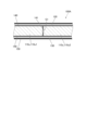
- Fig. 15 is a cross-sectional view showing a location where two graphite members are adjacent to each other in heat dissipation member 100A of embodiment 2.
- Heat dissipation member 100A of embodiment 2 may differ from embodiment 1 in the configuration of graphite block 110A, but the other configurations may be the same as embodiment 1. The differences will be described in detail below. That is, the substrate unit of embodiment 2 may differ from embodiment 1 in the configuration of heat dissipation member 100A (specifically, graphite block 110A), but the other configurations may be the same as embodiment 1.
- the graphite block 110A may include a plurality of graphite members 110u.
- the graphite member 110u is a single member that is formed when the member is released from the surrounding area by the bonding material. It is not easy to prepare a single large graphite block.
- graphite block 110A includes a plurality of graphite members 110u, it is possible to increase the dimensions of heat dissipation member 100A, and the degree of freedom in designing heat dissipation member 100A can be increased.
- the number of the graphite materials 110u is not particularly limited, but may be five or less. By having five or less, the proportion of areas with low thermal conductivity inside the graphite block 110A can be reduced.
- the areas with low thermal conductivity are the gap G1 that occurs between a pair of adjacent graphite materials 110u, or the bonding material 141 located in the gap G1 (see FIG. 15).
- the plurality of graphite materials 110u may be arranged in parallel in the first direction A1 in which the graphene is stacked. More specifically, the graphite block 110A may include a first graphite material 110u1, a second graphite material 110u2 arranged in parallel in the first direction A1 with respect to the first graphite material 110u1, and a bonding material 141 located between the first graphite material 110u1 and the second graphite material 110u2 and bonding the first graphite material 110u1 and the second graphite material 110u2.
- a gap G1 occurs between the plurality of graphite materials 110u.
- first direction A1 a direction of low thermal conductivity (i.e., first direction A1) can be generated throughout the graphite block 110A, as in embodiment 1. Therefore, when placing equipment or the like that should not be affected by heat to the sides of the graphite block 110A, the effect of heat from the graphite block 110A on the equipment or the like can be reduced by placing the equipment or the like in the direction of low thermal conductivity. This makes it possible to eliminate or simplify the insulation structure for reducing the effect of heat on the equipment or the like.
- the gap G1 may be an air gap.
- the bonding material 141 may be located in at least a portion of the gap G1.
- the bonding material 141 may substantially fill the gap G1 (for example, the bonding material 141 may be located in an area of 90% or more of the cross section).
- the bonding material 141 may be a brazing material, a solder material, or a resin material.
- the bonding material 141 may be made of the same material as the second bonding material 140 that bonds the first plate material 120 and the second plate material 130 to the graphite block 110A.
- the direction in which adjacent pairs of the plurality of graphite materials 110u face each other is not limited to the above direction.
- the plurality of graphite materials 110u may be arranged to face each other in a direction different from the direction in which the graphene is stacked (for example, the second direction A2 or the third direction A3).
- the arrangement direction (X direction) of element mounting portions 50 may preferably be a direction perpendicular to the extension direction (third direction A3) of the crystal plane in graphite block 110A, or more preferably, may be a direction inclined (a direction that is neither parallel nor perpendicular) to the extension direction (third direction A3) of the crystal plane in graphite block 110A.
- the inclination angle ⁇ may preferably be an angle at which the first heat transfer region Ra and the third heat transfer region Rc do not overlap, or more preferably, may be an angle at which the heat transfer region R is maximized.
- the shape and size of the element mounting portion 50, the spacing between the element mounting portions 50, etc. may be set so as to satisfy the condition that the first heat transfer region Ra and the third heat transfer region Rc do not overlap.
- the heat transfer region R through which heat of the electronic element 310 mounted on one element mounting portion 50 moves and the heat transfer region R through which heat of the electronic element 310 mounted on the other element mounting portion 50 moves do not have to overlap.
- Third Embodiment 16A and 16B are diagrams showing an example of a heat dissipation member 100B of embodiment 3, where FIG. 16A is an oblique view showing the configuration excluding the protective layer 150, and FIG. 16B is an oblique view showing the configuration excluding the protective layer 150, the first plate material 120, and the second plate material 130.
- Heat dissipation member 100B of embodiment 3 may differ from embodiments 1 and 2 in the configuration of graphite block 110B, but may be otherwise similar to embodiments 1 and 2. The differences will be described in detail below. That is, heat dissipation member 100B (specifically, graphite block 110B) of the substrate unit of embodiment 3 may differ from embodiments 1 and 2 in the configuration of heat dissipation member 100B, but may be otherwise similar to embodiments 1 and 2.
- Graphite block 110B may include a plurality of graphite materials 110u. As shown in FIG. 16A, the plurality of graphite materials 110u may be arranged in parallel in second direction A2. This configuration allows the dimensions of heat dissipation member 100B to be increased in second direction A2 (i.e., the direction from first plate material 120 to second plate material 130), and increases the design freedom of heat dissipation member 100B.
- the multiple graphite materials 110u When aligned in the second direction A2, the multiple graphite materials 110u may be arranged to face each other in any one direction along the crystal plane (i.e., the second direction A2, the third direction A3, etc., which have high thermal conductivity). This configuration allows for rapid conduction of heat from the first plate material 120 to the second plate material 130.
- first direction A1 in which graphene is stacked and the second direction A2 and third direction A3 along the crystal plane may not coincide between the multiple graphite materials 110u.
- a pair of adjacent graphite materials 110u are referred to as the first graphite material 110u and the second graphite material 110u.
- the direction A1a in which graphene is stacked in the first graphite material 110u and the direction A1b in which graphene is stacked in the second graphite material 110u may be in a twisted relationship with each other.
- the multiple graphite materials 110u may be joined via a joining material.
- the arrangement direction (X direction) of the element mounting portions 50 may preferably be a direction perpendicular to the extension direction (e.g., the third direction A3a) of the crystal plane of the graphite material 110u closest to the element mounting portion 50, or more preferably, may be a direction inclined (a direction that is neither parallel nor perpendicular) to the extension direction (e.g., the third direction A3a) of the crystal plane of the graphite material 110u closest to the element mounting portion 50.
- the inclination angle ⁇ may preferably be an angle at which the first heat transfer region Ra and the third heat transfer region Rc do not overlap in the graphite material 110u closest to the element mounting portion 50, or more preferably, may be an angle at which the heat transfer region R is maximized.
- the substrate unit 10 may be set so as to satisfy the condition that the first heat transfer region Ra and the third heat transfer region Rc do not overlap in the graphite material 110u closest to the element mounting portion 50. Furthermore, when the substrate unit 10 has two element mounting portions 50, in the graphite material 110u closest to the element mounting portions 50, the heat transfer region R through which heat of the electronic element 310 mounted on one element mounting portion 50 moves and the heat transfer region R through which heat of the electronic element 310 mounted on the other element mounting portion 50 moves do not have to overlap.
- FIGS. 17A and 17B are diagrams illustrating an example of a method for manufacturing a heat dissipation member. The following describes a method for manufacturing the heat dissipation member 100A of the second embodiment.
- the manufacturing method includes a graphite processing step J1, a graphite material combining and joining step J2, a cutting step J3, and a plating step J4.
- a processing machine such as a wire saw is used to cut the graphite unit 501 to produce multiple graphite materials 501u.
- the graphite unit 501 generally has two crystal faces, and the dimensions of the crystal faces are greater than the dimensions in the direction perpendicular to the crystal faces.
- the cut graphite material 501u may be cut so that the minimum width of the crystal faces is smaller than the minimum width of the cut surface (i.e., the crystal layer surface).
- the multiple graphite materials 501u are arranged in parallel in the orientation shown in embodiment 2. Furthermore, a first plate material 520 and a second plate material 530 are arranged on the multiple graphite materials 501u with a joining material therebetween, and the joining material is applied by heating and cooling. At this stage, the first plate material 520 and the second plate material 530 are joined to the multiple graphite materials 501u, and the joining material may enter the gaps G1 (see FIG. 15) between the multiple graphite materials 501u, joining the multiple graphite materials 501u to each other.
- the first plate 520, the plurality of graphite members 501u, and the second plate 530 joined together are cut to the dimensions of the first plate 120, the graphite block 110A, and the second plate 130 of the heat dissipation member 100A.
- the cutting direction in the cutting process J3 may be inclined with respect to the third direction A3.
- plating is applied to the outside of the structure cut in the cutting step J3.
- the plating is performed so as to cover at least the side surface 113 of the graphite block 110A.
- the plating may be performed on the entire surface including the outer surfaces of the first plate material 120 and the second plate material 130. As a result, the plating layer becomes the protective layer 150.
- the heat dissipation member 100A is manufactured by the above-mentioned steps J1 to J4.
- the heat dissipation member is not limited to the above configuration.
- the linear expansion coefficient of the first plate material and the second plate material may be greater than the linear expansion coefficient of the graphite block in both the first direction and the second direction.
- a resin material such as ABS resin or polybutylene terephthalate (PBT) may be used as the material of the first plate material and the second plate material.
- PBT polybutylene terephthalate
- the linear expansion coefficient of the graphite block 110 is less than 24 [10 ⁇ -6/K] in the first direction A1
- a metal material such as aluminum having a linear expansion coefficient greater than that of copper may be used as the material of the first plate material 120 and the second plate material 130. Even in this case, the same effect is achieved in that the configuration is the same as or similar to that of the above embodiment.
- the heat dissipation member and the board unit of the present disclosure are not limited to the heat dissipation members 100, 100A, and 100B and the board unit 10 of the above embodiments.
- the details shown in the embodiments can be appropriately changed without departing from the spirit of the invention. According to the present disclosure, a board unit and an electronic device with improved heat dissipation performance can be obtained.
- the board unit is A substrate; a heat dissipation member located on the substrate and including a carbon material; an element mounting portion located on the opposite side of the substrate with respect to the heat dissipation member; the element mounting portion and the substrate are thermally connected via the heat dissipation member, In the direction in which the substrate and the heat dissipation member are arranged, the heat dissipation member has a higher thermal conductivity than the substrate.
- the substrate unit of (1) above is
- the heat dissipation member is A graphite block having anisotropic thermal conductivity; a protective part covering the graphite block; the thermal conductivity of the graphite block in the alignment direction is higher than the thermal conductivity of the graphite block in one direction intersecting the alignment direction; In the arrangement direction, the thermal conductivity of the heat dissipation member is higher than the thermal conductivity of the protection portion, In the one direction, the thermal conductivity of the substrate is higher than the thermal conductivity of the heat dissipation member, and the thermal conductivity of the protection portion is higher than the thermal conductivity of the heat dissipation member.
- the substrate unit of (2) above is
- the heat dissipation member may further include a bonding material that is located between the substrate and the heat dissipation member and bonds the substrate and the heat dissipation member, In the one direction, the thermal conductivity of the bonding material is higher than the thermal conductivity of the graphite block.
- the substrate unit of (3) above is
- the bonding material is a first bonding material
- the heat dissipation member further includes a second bonding material located between the graphite block and the protective portion and bonding the graphite block and the protective portion, In the one direction, the thermal conductivity of the second bonding material is higher than the thermal conductivity of the graphite block; The melting point of the first bonding material is lower than the melting point of the second bonding material.
- the heat dissipation member further includes a submount substrate, the submount substrate being located on the heat dissipation member and including an insulating material, the protection portion of the heat dissipation member includes a metal, The element mounting portion is located on the heat dissipation member via the submount substrate.
- the substrate unit of (4) above is a submount substrate located on the heat dissipation member and including an insulating material; a third bonding material located between the heat dissipation member and the submount substrate and bonding the heat dissipation member and the submount substrate, the protection portion of the heat dissipation member includes a metal, the element mounting portion is located on the heat dissipation member via the submount substrate, The melting point of the third bonding material is lower than the melting point of the second bonding material.
- the graphite block has a first surface extending along a first direction, a second surface opposing the first surface, and a side surface located between the first surface and the second surface and extending along the second direction along which the first surface and the second surface oppose each other;
- the protective part is A first plate member fixed to the first surface;
- the graphite block has a structure in which a plurality of graphenes are stacked in the first direction.
- the substrate unit of (7) above is The side surface includes a first side surface extending along a third direction intersecting the first direction and the second direction, The surface roughness of the first side surface is less than the surface roughness of the first face.
- the side surface includes a second side surface extending along the first direction, the second side surface has a concave-convex structure including a plurality of concave portions, A portion of the protective layer is located within the recess.
- the graphite block is A first graphite material; a second graphite material aligned in the first direction relative to the first graphite material; and a bonding material located between the first graphite material and the second graphite material, bonding the first graphite material and the second graphite material.
- the protective layer covers the side surfaces as well as at least a portion of the first plate and at least a portion of the second plate.
- the first plate material and the second plate material are made of metal.
- the protective layer is a plating layer.
- the element mounting portion is located on the first surface or the second surface.
- the electronic device is Any one of the substrate units (1) to (15) above; an electronic element mounted on the element mounting portion; Equipped with.
- This disclosure can be used as a substrate unit and electronic device.
- Substrate unit 20 Substrate 30 Submount substrate 40 Third bonding material 50 Element mounting portion 50a First element mounting portion 50b Second element mounting portion 50c Third element mounting portion 60 First bonding material 100, 100A, 100B Heat dissipation member 110, 110A, 110B Graphite block 110u Graphite material 110u1 First graphite material 110u2 Second graphite material 111 First surface 112 Second surface 113 Side surface 113a First side surface 113b Second side surface 120 First plate material (protective portion) 130 Second plate material (protection part) 140 Second bonding material 141 Bonding material 150 Protective layer (protective part) 300 Electronic device 310 Electronic element 400 Heat dissipation structure A1 First direction A2 Second direction A3 Third direction F1 Recess
Landscapes
- Physics & Mathematics (AREA)
- Condensed Matter Physics & Semiconductors (AREA)
- General Physics & Mathematics (AREA)
- Electromagnetism (AREA)
- Optics & Photonics (AREA)
- Thermal Sciences (AREA)
- Engineering & Computer Science (AREA)
- Microelectronics & Electronic Packaging (AREA)
- Cooling Or The Like Of Semiconductors Or Solid State Devices (AREA)
Priority Applications (1)
| Application Number | Priority Date | Filing Date | Title |
|---|---|---|---|
| JP2025535824A JPWO2025023225A1 (https=) | 2023-07-25 | 2024-07-23 |
Applications Claiming Priority (2)
| Application Number | Priority Date | Filing Date | Title |
|---|---|---|---|
| JP2023-120366 | 2023-07-25 | ||
| JP2023120366 | 2023-07-25 |
Publications (1)
| Publication Number | Publication Date |
|---|---|
| WO2025023225A1 true WO2025023225A1 (ja) | 2025-01-30 |
Family
ID=94374564
Family Applications (1)
| Application Number | Title | Priority Date | Filing Date |
|---|---|---|---|
| PCT/JP2024/026227 Pending WO2025023225A1 (ja) | 2023-07-25 | 2024-07-23 | 基板ユニット及び電子装置 |
Country Status (2)
| Country | Link |
|---|---|
| JP (1) | JPWO2025023225A1 (https=) |
| WO (1) | WO2025023225A1 (https=) |
Citations (4)
| Publication number | Priority date | Publication date | Assignee | Title |
|---|---|---|---|---|
| JP2012222160A (ja) * | 2011-04-08 | 2012-11-12 | Nippon Soken Inc | 発熱体モジュール及びその製造方法、熱拡散部材 |
| JP2017112334A (ja) * | 2015-12-18 | 2017-06-22 | 株式会社サーモグラフィティクス | 熱伝導構造体、熱伝導構造体の製造方法、冷却装置、及び半導体モジュール |
| JP2021090046A (ja) * | 2019-11-25 | 2021-06-10 | 三菱マテリアル株式会社 | グラフェン接合体 |
| JP2022117959A (ja) * | 2021-02-01 | 2022-08-12 | 株式会社サーモグラフィティクス | グラファイト構造体、冷却装置、グラファイト構造体の製造方法 |
-
2024
- 2024-07-23 JP JP2025535824A patent/JPWO2025023225A1/ja active Pending
- 2024-07-23 WO PCT/JP2024/026227 patent/WO2025023225A1/ja active Pending
Patent Citations (4)
| Publication number | Priority date | Publication date | Assignee | Title |
|---|---|---|---|---|
| JP2012222160A (ja) * | 2011-04-08 | 2012-11-12 | Nippon Soken Inc | 発熱体モジュール及びその製造方法、熱拡散部材 |
| JP2017112334A (ja) * | 2015-12-18 | 2017-06-22 | 株式会社サーモグラフィティクス | 熱伝導構造体、熱伝導構造体の製造方法、冷却装置、及び半導体モジュール |
| JP2021090046A (ja) * | 2019-11-25 | 2021-06-10 | 三菱マテリアル株式会社 | グラフェン接合体 |
| JP2022117959A (ja) * | 2021-02-01 | 2022-08-12 | 株式会社サーモグラフィティクス | グラファイト構造体、冷却装置、グラファイト構造体の製造方法 |
Also Published As
| Publication number | Publication date |
|---|---|
| JPWO2025023225A1 (https=) | 2025-01-30 |
Similar Documents
| Publication | Publication Date | Title |
|---|---|---|
| US7745928B2 (en) | Heat dissipation plate and semiconductor device | |
| CN101794754B (zh) | 半导体装置 | |
| CN100578768C (zh) | 散热装置及功率模块 | |
| KR101017452B1 (ko) | 반도체 패키지 | |
| WO2024203810A1 (ja) | 伝熱部材及び電子装置 | |
| JP2003168769A (ja) | 電力用半導体装置 | |
| US20140117508A1 (en) | Semiconductor unit | |
| WO2018168591A1 (ja) | モジュール | |
| US8227913B2 (en) | Power semiconductor module comprising elastic housing for accommodating movement of individual substrate regions on a heat sink | |
| JP2005011922A (ja) | ヒートシンクを備えた両面銅貼り基板、およびこれを用いた半導体装置 | |
| WO2025023225A1 (ja) | 基板ユニット及び電子装置 | |
| WO2025023230A1 (ja) | 放熱構造及び基板ユニット | |
| JP2011018807A (ja) | パワーモジュール | |
| JP2018152408A (ja) | ヒートスプレッダ | |
| WO2008075409A1 (ja) | パワーモジュール用ベース、パワーモジュール用ベースの製造方法及びパ ワーモジュール | |
| WO2025023237A1 (ja) | 放熱部材及び電子装置 | |
| CN1835223B (zh) | 半导体装置及该半导体装置用绝缘衬底 | |
| JP4992302B2 (ja) | パワー半導体モジュール | |
| WO2025146813A1 (ja) | 伝熱部材および電子装置 | |
| JP2025106792A (ja) | 伝熱部材および電子装置 | |
| TWI851051B (zh) | 晶片與集成散熱器的封裝結構 | |
| JP2022014386A (ja) | 半導体装置 | |
| JP7415486B2 (ja) | ヒートシンク付絶縁回路基板及びその製造方法 | |
| JP2011096758A (ja) | 絶縁放熱基板 | |
| WO2025146815A1 (ja) | 伝熱部材および電子装置 |
Legal Events
| Date | Code | Title | Description |
|---|---|---|---|
| 121 | Ep: the epo has been informed by wipo that ep was designated in this application |
Ref document number: 24845601 Country of ref document: EP Kind code of ref document: A1 |
|
| ENP | Entry into the national phase |
Ref document number: 2025535824 Country of ref document: JP Kind code of ref document: A |
|
| WWE | Wipo information: entry into national phase |
Ref document number: 2025535824 Country of ref document: JP |
|
| NENP | Non-entry into the national phase |
Ref country code: DE |