WO2025023001A1 - 炭化珪素半導体装置 - Google Patents
炭化珪素半導体装置 Download PDFInfo
- Publication number
- WO2025023001A1 WO2025023001A1 PCT/JP2024/024715 JP2024024715W WO2025023001A1 WO 2025023001 A1 WO2025023001 A1 WO 2025023001A1 JP 2024024715 W JP2024024715 W JP 2024024715W WO 2025023001 A1 WO2025023001 A1 WO 2025023001A1
- Authority
- WO
- WIPO (PCT)
- Prior art keywords
- region
- silicon carbide
- conductivity type
- electric field
- main surface
- Prior art date
- Legal status (The legal status is an assumption and is not a legal conclusion. Google has not performed a legal analysis and makes no representation as to the accuracy of the status listed.)
- Pending
Links
Images



Definitions
- This disclosure relates to silicon carbide semiconductor devices.
- a trench-type MOSFET metal oxide semiconductor field effect transistor
- an electric field relaxation region is provided below a gate trench formed on the main surface.
- the silicon carbide semiconductor device disclosed herein comprises a silicon carbide substrate having a first main surface and a second main surface opposite to the first main surface, the silicon carbide substrate having a drift region having a first conductivity type, a body region provided on the drift region and having a second conductivity type different from the first conductivity type, a source region provided on the body region so as to be separated from the drift region and having the first conductivity type, a connection region provided below the body region, in contact with the body region and having the second conductivity type, and an electric field relaxation region provided below the connection region, in contact with the connection region and having the second conductivity type, and the silicon carbide substrate having a first main surface and a second main surface opposite to the first main surface, ...
- a gate trench is provided with a side surface that reaches the drift region and a bottom surface that is continuous with the side surface, a gate insulating film that contacts the side surface and the bottom surface of the gate trench, and a gate electrode that is provided on the gate insulating film so as to sandwich the gate insulating film between the gate trench and the silicon carbide substrate, the gate trench extends along a first axis parallel to the first main surface, the connection region is farther from the gate trench than the body region along a second axis that is parallel to the first main surface and perpendicular to the first axis, the electric field relaxation region is farther from the gate trench than the connection region along the second axis, and the first thickness of the electric field relaxation region is greater than the second thickness of the connection region.
- FIG. 1 is a diagram showing a configuration of an interlayer insulating film and a first main surface in a silicon carbide semiconductor device according to the first embodiment.
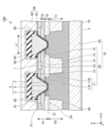
- FIG. 2 is a cross-sectional view showing the configuration of the silicon carbide semiconductor device according to the first embodiment.
- FIG. 3 is a schematic diagram showing the ranges of the connection region and the electric field relaxation region.
- FIG. 4 is a cross-sectional view showing a configuration of a silicon carbide semiconductor device according to the second embodiment.
- the objective of this disclosure is to provide a silicon carbide semiconductor device that can ensure the reliability of the gate insulating film while reducing the on-resistance.
- the XY plane view is referred to as a planar view
- the +Z direction may be referred to as the upper side, upper side, or upper side from an arbitrary point
- the -Z direction may be referred to as the lower side, lower side, or lower side.
- a gate trench is provided with a side surface extending through the gate trench to the drift region and a bottom surface connected to the side surface, a gate insulating film contacting the side surface and the bottom surface of the gate trench, and a gate electrode provided on the gate insulating film so as to sandwich the gate insulating film between the gate trench and the silicon carbide substrate, the gate trench extends along a first axis parallel to the first main surface, the connection region is farther from the gate trench than the body region along a second axis parallel to the first main surface and perpendicular to the first axis, the electric field relaxation region is farther from the gate trench than the connection region along the second axis, and the first thickness of the electric field relaxation region is greater than the second thickness of the connection region.
- connection region is farther from the gate trench along the second axis than the body region, the electric field relaxation region is farther from the gate trench along the second axis than the connection region, and the first thickness of the electric field relaxation region is greater than the second thickness of the connection region.
- the second thickness may be greater than the third thickness of the body region. In this case, it is easier to alleviate the voltage applied to the gate insulating film.
- the drift region may have a first semiconductor region in contact with the side surface and the body region, and a second semiconductor region provided between the first semiconductor region and the second main surface and in contact with the first semiconductor region, and a first effective concentration of the first conductivity type impurity in the first semiconductor region may be higher than a second effective concentration of the first conductivity type impurity in the second semiconductor region.
- an on-current is likely to flow over a wide range of the drift region, making it easier to reduce on-resistance.
- the lower end surface of the connection region may be closer to the second main surface than the bottom surface. In this case, it is easier to reduce the voltage applied to the gate insulating film.
- a plurality of the gate trenches may be provided on the first main surface at a constant first pitch, and in a cross-sectional view perpendicular to the first axis, the silicon carbide substrate may have the connection region on both sides of the gate trench, and the distance between the connection regions may be 0.5 times or less than the first pitch. In this case, noise during switching operation may be easily reduced.
- the third effective concentration of the second conductivity type impurity in the body region may be higher than a fourth effective concentration of the second conductivity type impurity in the connection region, and the fourth effective concentration may be higher than a fifth effective concentration of the second conductivity type impurity in the electric field relaxation region.
- the voltage applied to the gate insulating film is more easily relaxed.
- the first depth of the bottom surface relative to the first main surface may be smaller than the second depth of the lower end surface of the electric field relaxation region relative to the bottom surface. In this case, it is easier to relax the voltage applied to the gate insulating film.
- the conductivity type of the semiconductor between the bottom surface and the second main surface may be the first conductivity type. In this case, it is easier to reduce the on-resistance.
- the side of the gate trench may include a ⁇ 0-33-8 ⁇ plane.
- the ⁇ 0-33-8 ⁇ plane By including the ⁇ 0-33-8 ⁇ plane on the side, good mobility can be obtained on the side of the gate trench, and channel resistance can be reduced.
- FIG. 1 is a diagram showing a configuration of an interlayer insulating film and a first main surface in a silicon carbide semiconductor device according to the first embodiment.
- FIG. 2 is a cross-sectional view showing a configuration of the silicon carbide semiconductor device according to the first embodiment.
- FIG. 2 corresponds to a cross-sectional view taken along line II-II in FIG. 1.
- the silicon carbide semiconductor device 100 mainly includes a silicon carbide substrate 10, a gate insulating film 81, a gate electrode 82, an interlayer insulating film 83, a source electrode 60, a drain electrode 70, and a barrier metal film 84.
- the silicon carbide substrate 10 has a first main surface 1 and a second main surface 2 opposite to the first main surface 1.
- the first main surface 1 and the second main surface 2 are parallel to the XY plane, and the first main surface 1 is in the +Z direction when viewed from the second main surface 2.
- the silicon carbide substrate 10 includes a silicon carbide single crystal substrate 50 and a silicon carbide epitaxial layer 40 on the silicon carbide single crystal substrate 50.
- the silicon carbide epitaxial layer 40 constitutes the first main surface 1, and the silicon carbide single crystal substrate 50 constitutes the second main surface 2.
- the silicon carbide single crystal substrate 50 and the silicon carbide epitaxial layer 40 are composed of, for example, hexagonal silicon carbide of polytype 4H.
- the silicon carbide single crystal substrate 50 contains n-type impurities such as nitrogen (N) and has an n-type conductivity type (first conductivity type).
- the first main surface 1 is a ⁇ 0001 ⁇ plane or a ⁇ 0001 ⁇ plane tilted at an off angle of 8° or less in the off direction.
- the first main surface 1 is a (000-1) plane or a (000-1) plane tilted at an off angle of 8° or less in the off direction.
- the off direction may be, for example, the ⁇ 11-20> direction or the ⁇ 1-100> direction.
- the off angle may be, for example, 1° or more, or 2° or more.
- the off angle may be 6° or less, or 4° or less.
- the silicon carbide epitaxial layer 40 mainly has a drift region 11, a body region 12, a source region 13, a connection region 14, an electric field relaxation region 15, and a contact region 18.
- the drift region 11 contains n-type impurities such as nitrogen or phosphorus (P) and has n-type conductivity.
- the drift region 11 is provided on a silicon carbide single crystal substrate 50.
- the drift region 11 mainly has a first region 11A and a second region 11B.
- the body region 12 contains p-type impurities such as aluminum (Al) and has a p-type conductivity.
- the body region 12 is provided on the drift region 11.
- the third thickness T3 of the body region 12 is 100 nm or more and 1000 nm or less.
- the source region 13 contains n-type impurities such as nitrogen or phosphorus, and has n-type conductivity.
- the source region 13 is provided on the body region 12.
- the source region 13 is separated from the drift region 11 by the body region 12.
- the source region 13 constitutes the first main surface 1.
- the first main surface 1 is provided with a plurality of gate trenches 5 defined by side surfaces 3 and bottom surfaces 4.
- the gate trenches 5 extend, for example, along the Y axis.
- a plurality of gate trenches 5 are provided at regular intervals (first pitch P1) along the X axis.
- the side surfaces 3 penetrate the source region 13, the body region 12, and a part of the drift region 11, and reach the drift region 11.
- the bottom surfaces 4 are continuous with the side surfaces 3.
- the bottom surfaces 4 are located in the drift region 11. For example, the bottom surfaces 4 are parallel to the first main surface 1 and the second main surface 2.
- the angle ⁇ 1 of the side surfaces 3 with respect to a virtual plane 31 including the bottom surfaces 4 is, for example, 45° or more and 65° or less.
- the angle ⁇ 1 may be, for example, 50° or more.
- the angle ⁇ 1 may be, for example, 60° or less.
- the side surfaces 3 preferably have a ⁇ 0-33-8 ⁇ plane.
- the ⁇ 0-33-8 ⁇ plane is a crystal plane that provides excellent mobility.
- the Y-axis is an example of the first axis
- the X-axis is an example of the second axis.
- Multiple gate trenches 5 may be arranged at regular intervals along the Y axis. When multiple gate trenches 5 are arranged at regular intervals along the Y axis, a portion of the contact region 18 may be located between adjacent gate trenches 5 along the Y axis. Multiple gate trenches 5 may be provided in an array.
- the connection region 14 contains p-type impurities such as aluminum and has a p-type conductivity.
- the connection region 14 is located between adjacent gate trenches 5 along the X-axis in a plan view perpendicular to the first main surface 1.
- the connection region 14 is away from the gate trench 5.
- the body region 12 is exposed to the side surface 3 of the gate trench 5.
- the connection region 14 is farther from the gate trench 5 along the X-axis than the body region 12.
- the connection region 14 is located below the body region 12 and contacts the body region 12.
- the connection region 14 overlaps the contact region 18 in a plan view perpendicular to the first main surface 1.
- the connection region 14 may be in contact with the body region 12 and the contact region 18.
- the connection region 14 may extend along the Y-axis.
- a plurality of connection regions 14 are arranged at regular intervals along the X-axis.
- a plurality of connection regions 14 may be provided in a stripe pattern.
- the second thickness T2 of the connection region 14 is 100 nm or more and 1000 nm or less.
- the second thickness T2 of the connection region 14 may be greater than the third thickness T3 of the body region 12.
- the electric field relaxation region 15 contains p-type impurities such as aluminum and has a p-type conductivity. In a plan view perpendicular to the first main surface 1, the electric field relaxation region 15 is between adjacent gate trenches 5 along the X-axis. The electric field relaxation region 15 is farther away from the gate trench 5. The electric field relaxation region 15 is farther away from the gate trench 5 along the X-axis than the connection region 14 is. The electric field relaxation region 15 is below the connection region 14 and contacts the connection region 14. In a plan view perpendicular to the first main surface 1, the electric field relaxation region 15 overlaps the contact region 18 and the connection region 14. The electric field relaxation region 15 may extend along the Y-axis.
- a plurality of electric field relaxation regions 15 are arranged at regular intervals along the X-axis.
- a plurality of electric field relaxation regions 15 may be provided in a stripe pattern.
- the first thickness T1 of the electric field relaxation region 15 may be 1000 nm or more and 5000 nm or less, and may be 1200 nm or more and 2500 nm or less.
- the first thickness T1 of the electric field relaxation region 15 is greater than the second thickness T2 of the connection region 14.
- the electric field relaxation region 15 can be formed, for example, by channeling implantation.
- connection region 14 is between the electric field relaxation region 15 and the body region 12.
- the contact region 18, the body region 12, the connection region 14 and the electric field relaxation region 15 are electrically connected to each other.
- the first region 11A of the drift region 11 is exposed to the side surface 3 and contacts the body region 12 and the connection region 14.
- the thickness of the first region 11A is, for example, 0.1 ⁇ m or more and 0.6 ⁇ m or less.
- the second region 11B of the drift region 11 may contact the silicon carbide single crystal substrate 50.
- the first region 11A is between the second region 11B and the body region 12.
- the lower end surface of the first region 11A contacts the upper end surface of the second region 11B.
- the second region 11B may be exposed to the side surface 3.
- the second region 11B may be exposed to the bottom surface 4.
- the lower end surface of the first region 11A may be on an imaginary plane 31 including the bottom surface 4, or may be closer to the first main surface 1 than the imaginary plane 31.
- the first region 11A is an example of a first semiconductor region
- the second region 11B is an example of a second semiconductor region.
- the second effective concentration of n-type impurities in the second region 11B is lower than the first effective concentration of n-type impurities in the first region 11A.
- the second effective concentration is 1 ⁇ 10 16 cm -3 or more and 1 ⁇ 10 17 cm -3 or less
- the first effective concentration is 1 ⁇ 10 17 cm -3 or more and 1 ⁇ 10 18 cm -3 or less.
- the first region 11A is sometimes called a current diffusion region.
- the conductivity type of the silicon carbide substrate 10 between the bottom surface 4 and the second main surface 2 is n-type.
- the Z axis there is no semiconductor with a p-type conductivity between the bottom surface 4 and the second main surface 2.
- the Z axis is an example of a third axis.
- the gate insulating film 81 is, for example, an oxide film.
- the gate insulating film 81 is made of, for example, a material containing silicon dioxide.
- the gate insulating film 81 contacts the side surface 3 and the bottom surface 4.
- the gate insulating film 81 contacts the drift region 11 at the bottom surface 4.
- the gate insulating film 81 contacts the second region 11B at the bottom surface 4.
- the gate insulating film 81 contacts the source region 13, the body region 12, and the drift region 11 at the side surface 3.
- the gate insulating film 81 contacts the first region 11A and the second region 11B at the side surface 3. As long as the gate insulating film 81 contacts the first region 11A at the side surface 3, it does not have to contact the second region 11B.
- the gate insulating film 81 may contact the source region 13 at the first main surface 1.
- the gate electrode 82 is provided on the gate insulating film 81.
- the gate electrode 82 is made of, for example, polysilicon (polySi) containing conductive impurities.
- the gate electrode 82 is disposed inside the gate trench 5.
- the gate electrode 82 faces the side surface 3 and the bottom surface 4. A portion of the gate electrode 82 may face the first main surface 1.
- the gate electrode 82 extends along the Y-axis. In a plan view perpendicular to the first main surface 1, the gate electrode 82 may overlap multiple gate trenches 5.
- the interlayer insulating film 83 covers the gate electrode 82.
- the interlayer insulating film 83 is in contact with the gate electrode 82 and the gate insulating film 81.
- the interlayer insulating film 83 is, for example, an oxide film.
- the interlayer insulating film 83 is made of, for example, a material containing silicon dioxide.
- the interlayer insulating film 83 electrically insulates the gate electrode 82 and the source electrode 60 from each other.
- a part of the interlayer insulating film 83 may be provided inside the gate trench 5.
- the upper surface of the interlayer insulating film 83 may be a curved surface whose curvature changes continuously.
- the upper surface of the interlayer insulating film 83 may be a curved surface that is convex in the +Z direction above the gate trench 5.
- Contact holes 90 are formed in the interlayer insulating film 83 and the gate insulating film 81 at regular intervals along the X-axis.
- the contact holes 90 are arranged such that the gate trench 5 is located between adjacent contact holes 90 along the X-axis.
- the contact holes 90 extend along the Y-axis. Through the contact holes 90, the source region 13 and the contact region 18 are exposed from the interlayer insulating film 83 and the gate insulating film 81.
- the barrier metal film 84 covers the upper surface of the interlayer insulating film 83 and the side surface of the gate insulating film 81.
- the barrier metal film 84 is in contact with the interlayer insulating film 83 and the gate insulating film 81.
- the barrier metal film 84 is made of a material containing, for example, titanium nitride (TiN).
- the source electrode 60 is in contact with the first main surface 1.
- the source electrode 60 has a contact electrode 61 provided in the contact hole 90 and a source wiring 62.
- the contact electrode 61 is in contact with the source region 13 and the contact region 18 on the first main surface 1.
- the contact electrode 61 is made of a material containing nickel silicide (NiSi), for example.
- the contact electrode 61 may be made of a material containing titanium (Ti), aluminum, and silicon.
- the contact electrode 61 is in ohmic contact with the source region 13 and the contact region 18.
- the source wiring 62 covers the upper surface and side surfaces of the barrier metal film 84 and the upper surface of the contact electrode 61.
- the source wiring 62 is in contact with the barrier metal film 84 and the contact electrode 61.
- the source wiring 62 is made of a material containing aluminum, for example.
- the drain electrode 70 is in contact with the second main surface 2.
- the drain electrode 70 is in contact with the silicon carbide single crystal substrate 50 at the second main surface 2.
- the drain electrode 70 is electrically connected to the drift region 11.
- the drain electrode 70 is made of a material containing nickel silicide, for example.
- the drain electrode 70 may be made of a material containing titanium, aluminum, and silicon.
- the drain electrode 70 is in ohmic contact with the silicon carbide single crystal substrate 50.
- a buffer layer containing n-type impurities such as nitrogen and having n-type conductivity may be provided between the silicon carbide single crystal substrate 50 and the drift region 11. Also, a passivation film covering a portion of the source electrode 60 may be provided.
- the effective concentration of the p-type impurity in the contact region 18 may be higher than the effective concentration of the p-type impurity in the body region 12.
- the effective concentration of the p-type impurity in the contact region 18 is, for example, 1 ⁇ 10 18 cm ⁇ 3 or more and 1 ⁇ 10 20 cm ⁇ 3 or less
- the effective concentration of the p-type impurity in the body region 12 is, for example, 5 ⁇ 10 17 cm ⁇ 3 or more and 1 ⁇ 10 18 cm ⁇ 3 or less.
- the effective concentration of n-type impurities in the source region 13 may be higher than the effective concentration of p-type impurities in the body region 12.
- the effective concentration of n-type impurities in the source region 13 is, for example, about 1 ⁇ 10 19 cm ⁇ 3 .
- the effective concentration of p-type impurities in the connection region 14 and the effective concentration of p-type impurities in the electric field relaxation region 15 are, for example, not less than 5 ⁇ 10 17 cm ⁇ 3 and not more than 5 ⁇ 10 18 cm ⁇ 3 .
- the effective concentration of a first conductivity type impurity is the concentration obtained by subtracting the concentration of a second conductivity type impurity from the concentration of a first conductivity type impurity
- the effective concentration of a second conductivity type impurity is the concentration obtained by subtracting the concentration of a first conductivity type impurity from the concentration of a second conductivity type impurity.
- the effective concentrations can be measured, for example, using a scanning capacitance microscope (SCM).
- Figure 3 is a schematic diagram showing the scope of the connection region 14 and the electric field relaxation region 15.
- the drift region 11 has an n-type conductivity, and the body region 12, the connection region 14, and the electric field relaxation region 15 have a p-type conductivity. Therefore, the boundaries between the drift region 11 and the body region 12, between the drift region 11 and the connection region 14, and between the drift region 11 and the electric field relaxation region 15 are clear.
- the upper end surface 21 of the drift region 11 is in contact with the lower end surface 22 of the body region 12.
- the upper end surface 23 of the connection region 14 is in the same plane as the upper end surface 21 of the drift region 11.
- the center of an osculating circle 33 that touches the curves representing the p-type region (connection region 14 or electric field relaxation region 15) and the drift region 11 in a cross-sectional view perpendicular to the Y axis is moved toward the second main surface, the center of the osculating circle 33 moves from the p-type region to the drift region 11 on a surface that is a certain distance away from the first main surface 1.
- the lower end surface 24 of the connection region 14 and the upper end surface 25 of the electric field relaxation region 15 are located on this surface.
- the lower end surface 24 of the connection region 14 may be closer to the second main surface 2 than the bottom surface 4.
- the lower end surface 26 of the electric field relaxation region 15 is a surface that faces the silicon carbide single crystal substrate 50.
- connection region 14 is farther from the gate trench 5 than the body region 12 along the X-axis, and the electric field relaxation region 15 is farther from the gate trench 5 than the connection region 14 along the X-axis.
- the first thickness T1 of the electric field relaxation region 15 is greater than the second thickness T2 of the connection region 14. This allows the on-resistance to be reduced while relaxing the voltage applied to the gate insulating film 81. That is, it is possible to ensure the reliability of the gate insulating film 81 and reduce the on-resistance at the same time.
- the on-resistance can be reduced without widening the first region 11A to an extent that may cause an increase in noise during switching operation. Therefore, an increase in noise during switching operation can be avoided.
- a source trench is formed between the gate trenches, a source electrode is provided in the source trench, and a deep well region is provided around the source trench, the drain breakdown voltage may decrease, but in this embodiment, the decrease in drain breakdown voltage associated with the deep well region can be avoided.
- the conductivity type of the semiconductor (silicon carbide substrate 10) between the bottom surface 4 and the second main surface 2 along the Z axis is n-type and no semiconductor with a conductivity type of p-type exists between the bottom surface 4 and the second main surface 2, the on-resistance is easier to reduce.
- the voltage applied to the gate insulating film 81 is more easily alleviated.
- the on-current is more likely to flow over a wide range of the drift region 11, making it easier to reduce the on-resistance.
- the voltage applied to the gate insulating film 81 is more easily alleviated.
- the distance L1 between the two connection regions 14 sandwiching the gate trench 5 in a plan view perpendicular to the first main surface 1 may be, for example, 0.5 times or less the first pitch P1.
- the distance L1 is 0.5 times or less the first pitch P1, it is easy to reduce noise during switching operations.
- the third effective concentration of the p-type impurity in the body region 12 may be higher than the fourth effective concentration of the p-type impurity in the connection region 14, and the fourth effective concentration may be higher than the fifth effective concentration of the p-type impurity in the electric field relaxation region 15.
- the third effective concentration is higher than the fourth effective concentration and the fourth effective concentration is higher than the fifth effective concentration, the voltage applied to the gate insulating film 81 is more easily relaxed.
- the first depth D1 of the bottom surface 4 relative to the first main surface 1 may be smaller than the second depth D2 of the lower end surface 26 of the electric field relaxation region 15 relative to the bottom surface 4.
- the voltage applied to the gate insulating film 81 is more easily relaxed.
- the second depth D2 When the second depth D2 is 2 ⁇ m or more, the voltage applied to the gate insulating film 81 is more easily alleviated.
- the second depth D2 may be 2.5 ⁇ m or more, or 3 ⁇ m or more.
- Fig. 4 is a cross-sectional view showing the configuration of a silicon carbide semiconductor device according to the second embodiment.
- the electric field relaxation region 15 is formed wider than in the first embodiment. More specifically, in an imaginary plane 32 that is half (D2/2) of the second depth D2 from the bottom surface 4, the first width W1 of the electric field relaxation region 15 is larger than the second width W2 of the drift region 11 between adjacent electric field relaxation regions 15 in a cross-sectional view perpendicular to the Y axis.
- the second embodiment also provides the same effect as the first embodiment.
- the first width W1 is greater than the second width W2 in the imaginary plane 32, it is easier to reduce the voltage applied to the gate insulating film 81, and it is easier to reduce noise during switching operations.
Landscapes
- Electrodes Of Semiconductors (AREA)
Priority Applications (3)
| Application Number | Priority Date | Filing Date | Title |
|---|---|---|---|
| CN202480042705.1A CN121420644A (zh) | 2023-07-21 | 2024-07-09 | 碳化硅半导体器件 |
| JP2025535701A JPWO2025023001A1 (https=) | 2023-07-21 | 2024-07-09 | |
| DE112024003047.5T DE112024003047T5 (de) | 2023-07-21 | 2024-07-09 | Siliziumkarbid-Halbleiterbauelemente |
Applications Claiming Priority (2)
| Application Number | Priority Date | Filing Date | Title |
|---|---|---|---|
| JP2023119164 | 2023-07-21 | ||
| JP2023-119164 | 2023-07-21 |
Publications (1)
| Publication Number | Publication Date |
|---|---|
| WO2025023001A1 true WO2025023001A1 (ja) | 2025-01-30 |
Family
ID=94374319
Family Applications (1)
| Application Number | Title | Priority Date | Filing Date |
|---|---|---|---|
| PCT/JP2024/024715 Pending WO2025023001A1 (ja) | 2023-07-21 | 2024-07-09 | 炭化珪素半導体装置 |
Country Status (4)
| Country | Link |
|---|---|
| JP (1) | JPWO2025023001A1 (https=) |
| CN (1) | CN121420644A (https=) |
| DE (1) | DE112024003047T5 (https=) |
| WO (1) | WO2025023001A1 (https=) |
Citations (7)
| Publication number | Priority date | Publication date | Assignee | Title |
|---|---|---|---|---|
| JP2015162579A (ja) * | 2014-02-27 | 2015-09-07 | 住友電気工業株式会社 | 半導体装置 |
| JP2016066780A (ja) * | 2014-09-16 | 2016-04-28 | 株式会社デンソー | 炭化珪素半導体装置およびその製造方法 |
| JP2017059570A (ja) * | 2015-09-14 | 2017-03-23 | 株式会社東芝 | 半導体装置 |
| WO2018042835A1 (ja) * | 2016-08-31 | 2018-03-08 | 住友電気工業株式会社 | 炭化珪素半導体装置およびその製造方法 |
| JP2018206923A (ja) * | 2017-06-02 | 2018-12-27 | 富士電機株式会社 | 絶縁ゲート型半導体装置及びその製造方法 |
| WO2020110514A1 (ja) * | 2018-11-29 | 2020-06-04 | 富士電機株式会社 | 超接合炭化珪素半導体装置および超接合炭化珪素半導体装置の製造方法 |
| JP2023139376A (ja) * | 2022-03-22 | 2023-10-04 | 国立研究開発法人産業技術総合研究所 | 炭化珪素半導体装置 |
Family Cites Families (1)
| Publication number | Priority date | Publication date | Assignee | Title |
|---|---|---|---|---|
| JP7541315B2 (ja) | 2022-02-16 | 2024-08-28 | プライムプラネットエナジー&ソリューションズ株式会社 | ニッケル鉱からのニッケルの浸出方法および硫酸ニッケルの製造方法 |
-
2024
- 2024-07-09 DE DE112024003047.5T patent/DE112024003047T5/de active Pending
- 2024-07-09 CN CN202480042705.1A patent/CN121420644A/zh active Pending
- 2024-07-09 JP JP2025535701A patent/JPWO2025023001A1/ja active Pending
- 2024-07-09 WO PCT/JP2024/024715 patent/WO2025023001A1/ja active Pending
Patent Citations (7)
| Publication number | Priority date | Publication date | Assignee | Title |
|---|---|---|---|---|
| JP2015162579A (ja) * | 2014-02-27 | 2015-09-07 | 住友電気工業株式会社 | 半導体装置 |
| JP2016066780A (ja) * | 2014-09-16 | 2016-04-28 | 株式会社デンソー | 炭化珪素半導体装置およびその製造方法 |
| JP2017059570A (ja) * | 2015-09-14 | 2017-03-23 | 株式会社東芝 | 半導体装置 |
| WO2018042835A1 (ja) * | 2016-08-31 | 2018-03-08 | 住友電気工業株式会社 | 炭化珪素半導体装置およびその製造方法 |
| JP2018206923A (ja) * | 2017-06-02 | 2018-12-27 | 富士電機株式会社 | 絶縁ゲート型半導体装置及びその製造方法 |
| WO2020110514A1 (ja) * | 2018-11-29 | 2020-06-04 | 富士電機株式会社 | 超接合炭化珪素半導体装置および超接合炭化珪素半導体装置の製造方法 |
| JP2023139376A (ja) * | 2022-03-22 | 2023-10-04 | 国立研究開発法人産業技術総合研究所 | 炭化珪素半導体装置 |
Also Published As
| Publication number | Publication date |
|---|---|
| CN121420644A (zh) | 2026-01-27 |
| DE112024003047T5 (de) | 2026-05-07 |
| JPWO2025023001A1 (https=) | 2025-01-30 |
Similar Documents
| Publication | Publication Date | Title |
|---|---|---|
| JP7161043B2 (ja) | SiC半導体装置 | |
| US20070262390A1 (en) | Insulated gate semiconductor device | |
| US10777678B2 (en) | Semiconductor device | |
| JP7674656B2 (ja) | 炭化ケイ素半導体装置 | |
| US11189703B2 (en) | Semiconductor device with trench structure having differing widths | |
| US6930356B2 (en) | Power semiconductor device having high breakdown voltage, low on-resistance, and small switching loss and method of forming the same | |
| JP6064366B2 (ja) | 半導体装置 | |
| EP1936695B1 (en) | Silicon carbide semiconductor device | |
| WO2025023001A1 (ja) | 炭化珪素半導体装置 | |
| JP7803420B2 (ja) | 炭化珪素半導体装置 | |
| JP7819083B2 (ja) | 炭化ケイ素半導体装置 | |
| US20230299144A1 (en) | Silicon carbide semiconductor device | |
| WO2025121295A1 (ja) | 炭化珪素半導体装置 | |
| WO2025169858A1 (ja) | 炭化珪素半導体装置 | |
| JP2024153355A (ja) | 炭化珪素半導体装置 | |
| WO2023042508A1 (ja) | 炭化珪素半導体装置 | |
| JP2025101790A (ja) | 炭化珪素半導体装置 | |
| WO2025127078A1 (ja) | 炭化珪素半導体装置 | |
| JP2024047312A (ja) | 炭化珪素半導体装置 | |
| WO2025239371A1 (ja) | 炭化珪素半導体装置 | |
| JP2024124050A (ja) | 炭化珪素半導体装置 | |
| JP2024031657A (ja) | 炭化珪素半導体装置 | |
| JP2024124051A (ja) | 炭化珪素半導体装置 | |
| JP2025162418A (ja) | 炭化珪素半導体装置 | |
| WO2025173558A1 (ja) | 炭化珪素半導体装置 |
Legal Events
| Date | Code | Title | Description |
|---|---|---|---|
| ENP | Entry into the national phase |
Ref document number: 2025535701 Country of ref document: JP Kind code of ref document: A |
|
| WWE | Wipo information: entry into national phase |
Ref document number: 2025535701 Country of ref document: JP |
|
| WWE | Wipo information: entry into national phase |
Ref document number: 112024003047 Country of ref document: DE |