WO2025022695A1 - 光結合器、光電変換回路モジュール及び光トランシーバ - Google Patents
光結合器、光電変換回路モジュール及び光トランシーバ Download PDFInfo
- Publication number
- WO2025022695A1 WO2025022695A1 PCT/JP2024/004310 JP2024004310W WO2025022695A1 WO 2025022695 A1 WO2025022695 A1 WO 2025022695A1 JP 2024004310 W JP2024004310 W JP 2024004310W WO 2025022695 A1 WO2025022695 A1 WO 2025022695A1
- Authority
- WO
- WIPO (PCT)
- Prior art keywords
- side wall
- wall portion
- optical coupler
- optical
- width
- Prior art date
- Legal status (The legal status is an assumption and is not a legal conclusion. Google has not performed a legal analysis and makes no representation as to the accuracy of the status listed.)
- Pending
Links
Images






Classifications
-
- G—PHYSICS
- G02—OPTICS
- G02B—OPTICAL ELEMENTS, SYSTEMS OR APPARATUS
- G02B6/00—Light guides; Structural details of arrangements comprising light guides and other optical elements, e.g. couplings
- G02B6/24—Coupling light guides
- G02B6/42—Coupling light guides with opto-electronic elements
- G02B6/4292—Coupling light guides with opto-electronic elements the light guide being disconnectable from the opto-electronic element, e.g. mutually self aligning arrangements
-
- G—PHYSICS
- G02—OPTICS
- G02B—OPTICAL ELEMENTS, SYSTEMS OR APPARATUS
- G02B6/00—Light guides; Structural details of arrangements comprising light guides and other optical elements, e.g. couplings
- G02B6/24—Coupling light guides
- G02B6/26—Optical coupling means
-
- G—PHYSICS
- G02—OPTICS
- G02B—OPTICAL ELEMENTS, SYSTEMS OR APPARATUS
- G02B6/00—Light guides; Structural details of arrangements comprising light guides and other optical elements, e.g. couplings
- G02B6/24—Coupling light guides
- G02B6/42—Coupling light guides with opto-electronic elements
-
- G—PHYSICS
- G02—OPTICS
- G02B—OPTICAL ELEMENTS, SYSTEMS OR APPARATUS
- G02B6/00—Light guides; Structural details of arrangements comprising light guides and other optical elements, e.g. couplings
- G02B6/24—Coupling light guides
- G02B6/42—Coupling light guides with opto-electronic elements
- G02B6/4201—Packages, e.g. shape, construction, internal or external details
- G02B6/4204—Packages, e.g. shape, construction, internal or external details the coupling comprising intermediate optical elements, e.g. lenses, holograms
- G02B6/4214—Packages, e.g. shape, construction, internal or external details the coupling comprising intermediate optical elements, e.g. lenses, holograms the intermediate optical element having redirecting reflective means, e.g. mirrors, prisms for deflecting the radiation from horizontal to down- or upward direction toward a device
-
- G—PHYSICS
- G02—OPTICS
- G02B—OPTICAL ELEMENTS, SYSTEMS OR APPARATUS
- G02B6/00—Light guides; Structural details of arrangements comprising light guides and other optical elements, e.g. couplings
- G02B6/24—Coupling light guides
- G02B6/42—Coupling light guides with opto-electronic elements
- G02B6/4201—Packages, e.g. shape, construction, internal or external details
- G02B6/4219—Mechanical fixtures for holding or positioning the elements relative to each other in the couplings; Alignment methods for the elements, e.g. measuring or observing methods especially used therefor
- G02B6/4236—Fixing or mounting methods of the aligned elements
- G02B6/424—Mounting of the optical light guide
-
- G—PHYSICS
- G02—OPTICS
- G02B—OPTICAL ELEMENTS, SYSTEMS OR APPARATUS
- G02B6/00—Light guides; Structural details of arrangements comprising light guides and other optical elements, e.g. couplings
- G02B6/24—Coupling light guides
- G02B6/42—Coupling light guides with opto-electronic elements
- G02B6/4201—Packages, e.g. shape, construction, internal or external details
- G02B6/4246—Bidirectionally operating package structures
Definitions
- the present invention relates to an optical coupler, an optoelectronic conversion circuit module, and an optical transceiver.
- the optical module described in Patent Document 1 includes a package, a microlens, an optical fiber connector, a positioning means, and a fixing means.
- the package is equipped with at least one of a light emitting element and a light receiving element.
- the microlens is fixed to the package so as to be located on the optical path of the light emitted from the light emitting element and/or the light incident on the light receiving element.
- the optical fiber connector has an optical path changing section that changes the direction of the optical path so that the light emitting element and/or the light receiving element and the optical fiber are optically coupled via the microlens.
- the optical fiber connector is formed with a V-groove array for mounting the optical fiber.
- the positioning means mechanically positions the package and the optical fiber connector so that the light emitting element and/or the light receiving element and the optical fiber are optically coupled via the microlens and the optical path changing section.
- the fixing means fixes the optical fiber connector to the package in a detachable manner.
- the microlens, the optical path changing section, and the V-groove array are each separate members and are fixed by a fixing means. Therefore, it is difficult to maintain the positioning accuracy, and there is a risk of a decrease in the coupling efficiency between the light-emitting element and/or the light-receiving element, the microlens, the optical path changing section, and the optical fiber.
- disturbance light may enter the optical module from outside and mix with the light emitted from the optical fiber, lowering the S/N ratio.
- the object of the present invention is to provide an optical coupler, an optoelectronic conversion circuit module, and an optical transceiver that can suppress the decrease in coupling efficiency and suppress the decrease in the S/N ratio.
- An optical coupler comprises: An optical coupler integrally formed from a material including glass and a filler mixed in the glass, an optical fiber fixing portion that fixes each of a plurality of optical fibers that emit light in a first direction; a reflector that changes a traveling direction of the light emitted from any one of the plurality of optical fibers from the first direction to a second direction perpendicular to the first direction; a holder for holding the optical fiber fixing portion and the reflector, Equipped with The holding portion is a first side wall portion having a shape extending in a third direction perpendicular to the first direction and the second direction; a second side wall portion connected to the first side wall portion and having a shape extending in the first direction; a third side wall portion connected to the first side wall portion and having a shape extending in the first direction, the third side wall portion being located on an opposite side of the second side wall portion in the third direction with the optical fiber fixing portion and the reflecting portion interposed therebetween when viewed in the second direction;
- optical coupler, photoelectric conversion circuit module, and optical transceiver according to the present invention can suppress the decrease in coupling efficiency and suppress the decrease in the S/N ratio.
- FIG. 1 is a perspective view of an optical coupler 1.
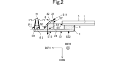
- FIG. 2 is a cross-sectional view of the optical coupler 1 and the optical fiber 5 .
- FIG. 3 is a plan view of the optical coupler 1 as viewed in the opposite direction to the second direction DIR2.
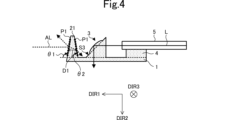
- FIG. 4 is a cross-sectional view of the optical coupler 1 and the optical fiber 5, showing how the ambient light AL is incident on the optical coupler 1.
- FIG. 5 is a cross-sectional view of the optical coupler 1 a and the optical fiber 5 .
- FIG. 6 is a cross-sectional view of the optical coupler 1 b and the optical fiber 5 .
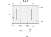
- FIG. 7 is a plan view of the optical coupler 1c viewed in the opposite direction to the second direction DIR2.
- FIG. 8 is a perspective view of the photoelectric conversion circuit module 10 and the optical fiber 5 .
- FIG. 9 is a cross-sectional view of the photoelectric conversion circuit module 10 and the optical fiber 5 taken along the line AA.
- FIG. 10 is a perspective view of the photoelectric conversion circuit module 10 a and the optical fiber 5 .
- FIG. 11 is a perspective view of the optical transceiver 100 and the optical fiber 5 .
- Fig. 1 is a perspective view of the optical coupler 1.
- Fig. 2 is a cross-sectional view of the optical coupler 1 and an optical fiber 5. Note that in Figs. 1 and 2, only a representative filler P1 among a plurality of fillers P1 is given a reference symbol. Also, in Fig. 2, the second side wall portion 22 and the third side wall portion 23 are omitted.
- Fig. 3 is a plan view of the optical coupler 1 viewed in the opposite direction to the second direction DIR2.
- directions are defined as follows. As shown in FIG. 1, the direction in which the optical fiber fixing portion 4 and the reflecting portion 3 are arranged in this order is defined as the first direction DIR1. The direction in which the reflecting portion 3 and the bottom portion 24 are arranged in this order is defined as the second direction DIR2. The direction in which the second side wall portion 22 and the third side wall portion 23 are arranged in this order is defined as the third direction DIR3. The first direction DIR1, the second direction DIR2, and the third direction DIR3 are mutually perpendicular.
- first direction DIR1, the second direction DIR2, and the third direction DIR3 in this specification are directions defined for the convenience of explanation, and do not have to coincide with the first direction DIR1, the second direction DIR2, and the third direction DIR3 when the optical coupler 1 is in use.
- the optical coupler 1 is a device for changing the direction of light emitted from an optical fiber and outputting it to a photoelectric conversion circuit or the like, or for changing the direction of light emitted from a photoelectric conversion circuit or the like and outputting it to an optical fiber.
- the optical coupler 1 changes the direction of light L emitted from an optical fiber 5 from a first direction DIR1 to a second direction DIR2.
- the optical coupler 1 has an incident surface S11 on which the light L emitted from the optical fiber 5 is incident, and an exit surface S12 from which the light L is output in the second direction DIR2.
- the structure of the optical coupler 1 will be described in detail below.
- the optical coupler 1 comprises a holding section 2, a reflecting section 3, and an optical fiber fixing section 4.
- the optical coupler 1 is integrally molded from glass containing a filler.
- the optical coupler 1 is also a single member.
- a single member means a member that has a structure that makes it impossible to separate without breaking. Therefore, for example, a member in which two pieces of resin are fixed with a screw is not a single member.
- the optical coupler 1 is integrally molded from a material including glass M1 and a plurality of fillers P1 mixed in the glass M1.
- Glass is an amorphous material that exhibits a glass transition phenomenon.
- the glass include simple oxide glasses such as SiO 2 , B 2 O 3 , P 2 O 5 , GeO 2 , and AS3O 3 ; silicate glasses such as Li 2 O-SiO 2 , Na 2 O-SiO 2 , and K 2 O-SiO 2 ; aluminosilicate glasses such as Na 2 O-Al 2 O 3 -SiO 2 and CaO-Al 2 O 3 -SiO 2 ; borate glasses such as Li 2 O-B 2 O 3 and Na 2 O-B 2 O 3 ; aluminoborate glasses such as CaO-Al 2 O 3 -B 2 O 3 ; and borosilicate glasses such as Na 2 O-Al 2 O 3 -B 2 O 3 -SiO 2 .
- the multiple fillers P1 are metal oxide particles such as crystalline silica, amorphous silica, alumina, magnesium oxide, and titanium oxide. Each of the multiple fillers P1 has a non-spherical shape. The multiple fillers P1 are dispersed throughout the glass M1. Each of the multiple fillers P1 may have a spherical shape. The multiple fillers P1 may be uniformly dispersed throughout the glass M1, or may be non-uniformly dispersed throughout the glass M1.
- the holding portion 2 holds each of the reflecting portion 3 and the optical fiber fixing portion 4.
- the holding portion 2 is connected to each of the reflecting portion 3 and the optical fiber fixing portion 4.
- the holding portion 2 includes a first side wall portion 21, a second side wall portion 22, a third side wall portion 23, and a bottom portion 24. Note that the holding portion 2 does not necessarily have to include the bottom portion 24.
- the first side wall portion 21 is connected to each of the second side wall portion 22, the third side wall portion 23, and the bottom portion 24. More specifically, the first side wall portion 21 has a shape extending in the third direction DIR3. In this embodiment, the end face of the first side wall portion 21 in the first direction DIR1 and the end face in the opposite direction to the first direction DIR1 (the first side surface and the second side surface aligned in the first direction DIR1) are inclined in a tapered shape as shown in FIG. 2. More specifically, when viewed in the third direction DIR3, the angle ⁇ 1 formed between the end face of the first side wall portion 21 in the first direction DIR1 and the first direction DIR1 is an obtuse angle.
- the angle ⁇ 2 formed between the end face of the first side wall portion 21 in the opposite direction to the first direction DIR1 and the first direction DIR1 is an acute angle. Therefore, the end face of the first side wall portion 21 in the first direction DIR1 and the end face of the first side wall portion 21 in the opposite direction to the first direction DIR1 are not parallel.
- the first width D1 of the first side wall portion 21 along the first direction DIR1 continuously increases toward the second direction DIR2.
- the end face of the first side wall portion 21 in the third direction DIR3 is connected to the third side wall portion 23 as shown in FIG. 1.
- the end face of the first side wall portion 21 in the opposite direction to the third direction DIR3 is connected to the second side wall portion 22.
- the end face of the first side wall portion 21 in the second direction DIR2 is connected to the bottom portion 24 as shown in FIG. 2.
- the filler P1 is exposed on the surface of the first side wall portion 21.
- the end face of the first side wall portion 21 in the first direction DIR1 and the end face in the opposite direction to the first direction DIR1 do not have to be inclined in a tapered shape. Also, the filler P1 does not have to be exposed on the surface of the first side wall portion 21.
- the second side wall portion 22 is connected to each of the first side wall portion 21, the bottom portion 24, the reflecting portion 3, and the optical fiber fixing portion 4. More specifically, the second side wall portion 22 is located in the opposite direction of the third direction DIR3 from the third side wall portion 23.
- the second side wall portion 22 has a shape extending in the first direction DIR1.
- the end face of the second side wall portion 22 in the third direction DIR3 and the end face in the opposite direction to the third direction DIR3 are inclined in a tapered shape.
- the angle ⁇ 3 formed between the end face of the second side wall portion 22 in the opposite direction to the third direction DIR3 and the third direction DIR3 is an acute angle.
- the angle ⁇ 4 between the end face of the second side wall portion 22 in the third direction DIR3 and the third direction DIR3 is an obtuse angle.
- the end face of the second side wall portion 22 in the opposite direction to the third direction DIR3 and the end face of the second side wall portion 22 in the third direction DIR3 are not parallel.
- the second width D2 of the second side wall portion 22 along the third direction DIR3 continuously increases toward the second direction DIR2.
- a portion of the end face of the second side wall portion 22 in the third direction DIR3 is connected to each of the end face of the first side wall portion 21 in the opposite direction to the third direction DIR3, the reflecting portion 3, and the optical fiber fixing portion 4.
- the end face of the second side wall portion 22 in the second direction DIR2 is connected to the bottom portion 24.
- the filler P1 is exposed on the surface of the second side wall portion 22.
- the end face of the second side wall portion 22 in the third direction DIR3 and the end face in the opposite direction to the third direction DIR3 do not have to be inclined in a tapered shape. Also, the filler P1 does not have to be exposed on the surface of the second side wall portion 22.
- the third side wall portion 23 is connected to each of the first side wall portion 21, the bottom portion 24, the reflecting portion 3 and the optical fiber fixing portion 4. More specifically, the third side wall portion 23 is located in the third direction DIR3 from the second side wall portion 22. When viewed in the second direction DIR2, the third side wall portion 23 is located on the opposite side along the third direction DIR3 of the second side wall portion 22, sandwiching the reflecting portion 3 and the optical fiber fixing portion 4.
- the third side wall portion 23 has a shape that extends in the first direction DIR1.
- the end face of the third side wall portion 23 in the third direction DIR3 and the end face in the opposite direction to the third direction DIR3 are inclined in a tapered shape.
- an angle ⁇ 5 formed between an end face of the third side wall portion 23 in the opposite direction to the third direction DIR3 and the third direction DIR3 is an acute angle.
- an angle ⁇ 6 formed between an end face of the third side wall portion 23 in the third direction DIR3 and the third direction DIR3 is an obtuse angle. Therefore, the end face of the third side wall portion 23 in the third direction DIR3 and the end face of the third side wall portion 23 in the opposite direction to the third direction DIR3 are not parallel.
- the third width D3 of the third side wall portion 23 along the third direction DIR3 continuously increases toward the second direction DIR2.
- a portion of the end face of the third side wall portion 23 in the opposite direction to the third direction DIR3 is connected to each of the end face of the first side wall portion 21 in the third direction DIR3, the reflecting portion 3, and the optical fiber fixing portion 4.
- the end face of the third side wall portion 23 in the second direction DIR2 is connected to the bottom portion 24.
- the filler P1 is exposed on the surface of the third side wall portion 23. Note that the end face of the third side wall portion 23 in the third direction DIR3 and the end face in the opposite direction to the third direction DIR3 (the third side surface and the fourth side surface aligned in the third direction DIR3) do not have to be inclined in a tapered shape.
- the filler P1 does not have to be exposed on the surface of the third side wall portion 23. It is sufficient that at least one of the first width D1 of the first side wall portion 21, the second width D2 of the second side wall portion 22, and the third width D3 of the third side wall portion 23 continuously increases in the second direction DIR2.
- the first width D1 of the first side wall portion 21, the second width D2 of the second side wall portion 22, and the third width D3 of the third side wall portion 23 are equal to each other.
- the bottom 24 is connected to each of the first side wall 21, the second side wall 22, the third side wall 23, the reflector 3, and the optical fiber fixing part 4. More specifically, the bottom 24 has a plate shape. In this embodiment, the bottom 24 has a rectangular shape when viewed in the second direction DIR2. A portion of the end face of the bottom 24 in the opposite direction to the second direction DIR2 is connected to each of the end face of the first side wall 21 in the second direction DIR2, the end face of the second side wall 22 in the second direction DIR2, the end face of the third side wall 23 in the second direction DIR2, the reflector 3, and the optical fiber fixing part 4. Note that the bottom 24 does not have to have a rectangular shape when viewed in the second direction DIR2.
- the optical fiber fixing part 4 fixes each of the five optical fibers 5.
- the optical fiber fixing part 4 is connected to each of the second side wall part 22, the third side wall part 23, and the bottom part 24. More specifically, the optical fiber fixing part 4 has a plate shape extending in the third direction DIR3.
- the optical fiber fixing part 4 is located between the second side wall part 22 and the third side wall part 23.
- the optical fiber fixing part 4 is also connected to each of the second side wall part 22 and the third side wall part 23. More specifically, the end of the optical fiber fixing part 4 along the opposite direction to the third direction DIR3 is connected to the second side wall part 22.
- the end of the optical fiber fixing part 4 along the third direction DIR3 is also connected to each of the third side wall parts 23.
- the end face of the optical fiber fixing part 4 in the second direction DIR2 is connected to the bottom part 24.
- Each of the five grooves G has a shape extending in the first direction DIR1.
- the five grooves G are lined up in the third direction DIR3.
- Five optical fibers 5 are fixed in each of the five grooves G as shown in FIG. 2.
- the five optical fibers 5 are lined up in the third direction DIR3.
- grooves G may not be provided on the end face of the optical fiber fixing part 4 in the opposite direction to the second direction DIR2.
- each of the five grooves G may have a U-shape when viewed in the first direction DIR1.
- the number of optical fibers 5 is not limited to five, and may be any number more than one.
- Each of the five optical fibers 5 has a shape that extends in the first direction DIR1.
- Each of the five optical fibers 5 has an end face S5 from which light L is emitted.
- the normal direction of the end face S5 of each of the five optical fibers 5 is the first direction DIR1.
- Each of the five optical fibers 5 emits light L in the first direction DIR1.
- the end face S5 of each of the five optical fibers 5 faces the reflecting section 3 with a gap between them. Light L emitted from any of the five optical fibers 5 travels in the first direction DIR1 and enters the reflecting section 3.
- the reflecting portion 3 is connected to each of the second side wall portion 22, the third side wall portion 23, and the bottom portion 24, as shown in FIG. 1.
- the reflecting portion 3 is located between the second side wall portion 22 and the third side wall portion 23.
- the reflecting portion 3 is also connected to each of the second side wall portion 22 and the third side wall portion 23. More specifically, the end portion of the reflecting portion 3 along the opposite direction to the third direction DIR3 is connected to the second side wall portion 22.
- the end portion of the reflecting portion 3 along the third direction DIR3 is also connected to the third side wall portion 23.
- the reflecting portion 3 changes the traveling direction of the light L incident from the incident surface S11 from the first direction DIR1 to the second direction DIR2.
- the reflecting portion 3 includes a prism portion 31 and five condenser lens portions 32.
- the number of condenser lens portions 32 is not limited to five, and may be any number.
- Prism portion 31 is connected to each of second side wall portion 22, third side wall portion 23, and bottom portion 24. More specifically, in this embodiment, prism portion 31 has a right-angled isosceles triangular prism shape extending in third direction DIR3. Prism portion 31 has prism portion entrance surface S2, prism portion reflection surface S3, and prism portion exit surface S4. Note that prism portion 31 does not have to have a right-angled isosceles triangular prism shape.
- the prism portion incident surface S2 is the end surface of the prism portion 31 in the opposite direction to the first direction DIR1.
- Light L emitted from any of the five optical fibers 5 enters the optical coupler 1 from the prism portion incident surface S2. Therefore, the prism portion incident surface S2 is the incident surface S11 of the optical coupler 1.
- the light L that enters the optical coupler 1 from the prism portion incident surface S2 passes through the inside of the prism portion 31.
- the prism portion reflecting surface S3 When viewed in the third direction DIR3, the prism portion reflecting surface S3 forms an angle of 135 degrees clockwise with respect to the first direction DIR1.
- the end of the prism portion reflecting surface S3 in the opposite direction to the second direction DIR2 is located in the opposite direction to the first direction DIR1 from the end of the prism portion reflecting surface S3 in the second direction DIR2.
- the prism portion reflecting surface S3 reflects the light L that has passed through the inside of the prism portion 31. As a result, the prism portion reflecting surface S3 changes the traveling direction of the light L from the first direction DIR1 to the second direction DIR2.
- the prism portion reflecting surface S3 corresponds to the "reflecting surface" of the present invention.
- the five focusing lens sections 32 are provided on the prism section reflecting surface S3.
- the five focusing lens sections 32 are lined up in the third direction DIR3.
- the surface of the focusing lens section 32 is aspheric.
- the surface of the focusing lens section 32 is ellipsoidal.
- the focusing lens section 32 focuses the light L that passes through the inside of the prism section 31 and travels in the first direction DIR1, while reflecting it toward the second direction DIR2.
- the focusing lens section 32 changes the traveling direction of the light L from a direction that includes a component of the first direction DIR1 to the second direction DIR2.
- the surface of the focusing lens section 32 does not have to be ellipsoidal.
- the prism portion exit surface S4 is an end surface of the prism portion 31 in the second direction DIR2.
- the prism portion exit surface S4 is connected to the bottom portion 24.
- the prism portion exit surface S4 emits light L that is reflected by the prism portion reflecting surface S3 or the focusing lens portion 32 and passes through the inside of the prism portion 31.
- the light L emitted from the prism portion exit surface S4 enters the bottom portion 24 from an end surface of the bottom portion 24 in the opposite direction of the second direction DIR2.
- Light L that enters the bottom 24 from the end face of the bottom 24 in the opposite direction of the second direction DIR2 passes through the inside of the bottom 24 and is emitted to the outside of the optical coupler 1 from the end face S1 of the bottom 24 in the second direction DIR2. Therefore, the end face S1 of the bottom 24 in the second direction DIR2 includes the emission face S12 of the optical coupler 1.
- the area of the end face S1 in the second direction DIR2 of the bottom 24 that overlaps with the reflecting portion 3 when viewed in the second direction DIR2 is defined as area A1.
- the area of the end face S1 in the second direction DIR2 of the bottom 24 that does not overlap with the reflecting portion 3 when viewed in the second direction DIR2 is defined as area A2.
- the end face S1 in the second direction DIR2 of the bottom 24 includes both area A1 and area A2.
- Light L is emitted from area A1 of the bottom 24 to the outside of the optical coupler 1. Therefore, area A1 is the emission surface S12.
- Area A2 is the mounting surface S22 for mounting the optical coupler 1 on a substrate when the optical coupler 1 is incorporated into a photoelectric conversion circuit module 10 described later or the like.
- the end face S1 in the second direction DIR2 of the bottom 24 includes the emission surface S12 and the mounting surface S22. That is, the mounting surface S22 is in the same plane as the emission surface S12.
- the optical coupler 1 is manufactured by irradiating and exposing a photosensitive glass paste containing glass M1 and a plurality of fillers P1 mixed into the glass M1 to ultraviolet light.
- the photosensitive glass paste may contain additives such as a dispersant and a light absorber in addition to the glass M1 and the plurality of fillers P1 mixed into the glass M1.
- a light-transmitting substrate having a first main surface and a second main surface aligned in the second direction DIR2 is prepared.
- a photosensitive glass paste is applied to the first main surface of the light-transmitting substrate.
- a mask is placed on the second main surface of the light-transmitting substrate.
- the second main surface of the light-transmitting substrate is irradiated with ultraviolet light to expose the photosensitive glass paste. This causes the photosensitive glass paste to become photosensitive.
- the mask is removed from the second main surface of the light-transmitting substrate, and the photosensitive glass paste is developed. More specifically, the photosensitive glass paste and the light-transmitting substrate are immersed in a developer.
- the photosensitive glass paste is a negative type, the exposed portion of the photosensitive glass paste remains, and the unexposed portion is removed.
- the photosensitive glass paste is a positive type, the exposed portion of the photosensitive glass paste is removed, and the unexposed portion remains. After development, the photosensitive glass paste and the light-transmitting substrate are washed and dried.
- the translucent substrate is removed from the developed photosensitive glass paste, and the photosensitive glass paste is hardened. More specifically, the photosensitive glass paste is fired to harden it. Through these steps, the optical coupler 1 is completed.
- the optical coupler 1 can suppress a decrease in coupling efficiency and also suppress a decrease in the S/N ratio. First, the ability of the optical coupler 1 to suppress a decrease in coupling efficiency will be described.
- the optical coupler 1 is integrally molded from a material that contains glass M1 and filler P1 that is mixed into the glass M1. Therefore, the optical coupler 1 allows each component, such as the microlens, the optical path changing section, and the V-groove array, to always be positioned in the same position, compared to when each component is a separate member. This makes it easy to maintain positioning accuracy and suppresses a decrease in coupling efficiency.
- the optical coupler 1 also includes a holding section 2 including a first side wall section 21, a second side wall section 22 connected to the first side wall section 21, and a third side wall section 23 connected to the first side wall section 21 and located on the opposite side of the second side wall section 22 along the third direction DIR3, sandwiching the reflecting section 3 and the optical fiber fixing section 4, as viewed in the second direction DIR2.
- a holding section 2 including a first side wall section 21, a second side wall section 22 connected to the first side wall section 21, and a third side wall section 23 connected to the first side wall section 21 and located on the opposite side of the second side wall section 22 along the third direction DIR3, sandwiching the reflecting section 3 and the optical fiber fixing section 4, as viewed in the second direction DIR2.
- a holding section 2 including a first side wall section 21, a second side wall section 22 connected to the first side wall section 21, and a third side wall section 23 connected to the first side wall section 21 and located on the opposite side of the second side wall section 22 along the third direction DIR3, sandwiching the reflecting section
- the ends of the optical fiber fixing section 4 and the reflecting section 3 along the third direction DIR3 are connected to the third side wall section 23.
- the optical fiber fixing part 4 or the reflecting part 3 tries to deform in the third direction DIR3 due to thermal expansion, the deformation of the optical fiber fixing part 4 or the reflecting part 3 in the third direction DIR3 is hindered by the third side wall part 23. Therefore, the optical fiber fixing part 4 and the reflecting part 3 are less likely to deform in the third direction DIR3.
- the ends of the optical fiber fixing part 4 and the reflecting part 3 along the opposite direction to the third direction DIR3 are connected to the second side wall part 22.
- the optical fiber fixing part 4 or the reflecting part 3 tries to deform in the opposite direction to the third direction DIR3 due to thermal expansion
- the deformation of the optical fiber fixing part 4 or the reflecting part 3 in the opposite direction to the third direction DIR3 is hindered by the second side wall part 22. Therefore, the optical fiber fixing part 4 and the reflecting part 3 are less likely to deform in the opposite direction to the third direction DIR3.
- the optical coupler 1 can suppress the optical fiber fixing part 4 and the reflecting part 3 from deforming due to thermal expansion. By suppressing the deformation of the optical fiber fixing part 4 and the reflecting part 3 due to thermal expansion, it is possible to suppress a change in the positional relationship between the optical fiber 5 and the reflecting part 3 and a decrease in coupling efficiency.
- FIG. 4 is a cross-sectional view of the optical coupler 1 and the optical fiber 5, showing how ambient light AL is incident on the optical coupler 1. Note that in FIG. 4, only a representative filler P1 out of the multiple fillers P1 is given a reference symbol. Below, we will explain using the first side wall portion 21 as an example, but the same applies to the second side wall portion 22 and the third side wall portion 23.
- the angle ⁇ 1 formed between the end face of the first side wall portion 21 in the first direction DIR1 and the first direction DIR1 is an obtuse angle.
- the direction of travel of the ambient light AL that enters the inside of the first side wall portion 21 is changed from a direction parallel to the first direction DIR1 to a direction that includes a component of the second direction DIR2 due to refraction by the end face in the first direction DIR1 of the first side wall portion 21.
- the angle ⁇ 2 between the end face of the first side wall portion 21 in the opposite direction to the first direction DIR1 and the first direction DIR1 is an acute angle when viewed in the third direction DIR3. Therefore, the traveling direction of the disturbance light AL traveling inside the first side wall portion 21 is changed to be closer to the second direction DIR2 due to refraction by the end face of the first side wall portion 21 in the opposite direction to the first direction DIR1. In this way, according to the optical coupler 1, the traveling direction of the disturbance light AL is changed from a direction parallel to the first direction DIR1 to a direction including a component of the second direction DIR2, and as a result, it is possible to suppress the disturbance light AL from being incident on the reflecting portion 3.
- the optical coupler 1 it is possible to suppress the disturbance light AL from being mixed into the light L emitted from the optical fiber 5 and the S/N ratio from decreasing. As a result, according to the optical coupler 1, it is possible to suppress the S/N ratio from decreasing.
- the optical coupler 1 can suppress the decrease in coupling efficiency and further suppress the decrease in the S/N ratio.
- the optical coupler 1 can further suppress a decrease in the S/N ratio.
- the first side wall portion 21 will be described as an example, but the same applies to the second side wall portion 22 and the third side wall portion 23.
- the filler P1 is exposed on the surface of the first side wall portion 21. Therefore, the filler P1 is exposed on the end face of the first side wall portion 21 in the first direction DIR1 and the end face of the first side wall portion 21 in the opposite direction to the first direction DIR1.
- the disturbance light AL incident on the first side wall portion 21 from the first direction DIR1 is scattered by the filler P1 exposed on the end face of the first side wall portion 21 in the first direction DIR1.
- the intensity of the disturbance light AL penetrating inside the first side wall portion 21 is reduced.
- the disturbance light AL traveling inside the first side wall portion 21 is scattered by the filler P1 exposed on the end face of the first side wall portion 21 in the opposite direction to the first direction DIR1.
- the optical coupler 1 can further suppress the disturbance light AL from mixing with the light L emitted from the optical fiber 5, thereby preventing a decrease in the S/N ratio.
- the optical coupler 1 can suppress the decrease in coupling efficiency and further suppress the decrease in the S/N ratio.
- FIG. 5 is a cross-sectional view of the optical coupler 1a and an optical fiber 5.
- a representative filler P1 among the multiple fillers P1 is given a reference symbol.
- the second side wall portion 22 and the third side wall portion 23 are omitted.
- the structure of the optical coupler 1a according to the first modified example only the parts different from the structure of the optical coupler 1 according to the first embodiment will be described, and the rest will be omitted.
- the end face of the first side wall portion 21 in the first direction DIR1 and the end face in the opposite direction to the first direction DIR1 are not tapered. More specifically, when viewed in the third direction DIR3, the angle ⁇ 2 between the end face of the first side wall portion 21 in the opposite direction to the first direction DIR1 and the first direction DIR1 is a right angle, while when viewed in the third direction DIR3, the angle ⁇ 1 between the end face of the first side wall portion 21 in the first direction DIR1 and the first direction DIR1 is an obtuse angle.
- the first width D1 of the first side wall portion 21 continuously increases toward the second direction DIR2.
- the end face of the second side wall portion 22 in the third direction DIR3 and the end face in the opposite direction to the third direction DIR3 do not have to be inclined in a tapered shape.
- the angle ⁇ 4 between the end face of the second side wall portion 22 in the third direction DIR3 and the third direction DIR3 may be a right angle when viewed in the first direction DIR1
- the angle ⁇ 3 between the end face of the second side wall portion 22 in the opposite direction to the third direction DIR3 and the third direction DIR3 may be an acute angle when viewed in the first direction DIR1.
- the second width D2 of the second side wall portion 22 continuously increases toward the second direction DIR2.
- the end face of the third side wall portion 23 in the third direction DIR3 and the end face in the opposite direction to the third direction DIR3 do not have to be inclined in a tapered shape. More specifically, when viewed in the first direction DIR1, the angle ⁇ 5 between the end face of the third side wall portion 23 in the opposite direction to the third direction DIR3 and the third direction DIR3 may be a right angle, while the angle ⁇ 6 between the end face of the third side wall portion 23 in the third direction DIR3 and the third direction DIR3 may be an obtuse angle when viewed in the first direction DIR1. Even in this case, as in the optical coupler 1, the third width D3 of the third side wall portion 23 continuously increases toward the second direction DIR2.
- optical coupler 1a described above also has the same effect as the optical coupler 1.
- FIG. 6 is a cross-sectional view of the optical coupler 1b and an optical fiber 5.
- a representative filler P1 among the multiple fillers P1 is given a reference symbol.
- the second side wall portion 22 and the third side wall portion 23 are omitted.
- the structure of the optical coupler 1b according to the second modified example only the parts different from the structure of the optical coupler 1 according to the first embodiment will be described, and the rest will be omitted.
- the end face of the first side wall portion 21 in the first direction DIR1 and the end face in the opposite direction to the first direction DIR1 are not tapered. More specifically, when viewed in the third direction DIR3, the angle ⁇ 1 between the end face of the first side wall portion 21 in the first direction DIR1 and the first direction DIR1 is a right angle, while when viewed in the third direction DIR3, the angle ⁇ 2 between the end face of the first side wall portion 21 in the opposite direction to the first direction DIR1 and the first direction DIR1 is an acute angle.
- the first width D1 of the first side wall portion 21 continuously increases toward the second direction DIR2.
- the end face of the second side wall portion 22 in the third direction DIR3 and the end face in the opposite direction to the third direction DIR3 do not have to be inclined in a tapered shape. More specifically, when viewed in the first direction DIR1, the angle ⁇ 3 between the end face of the second side wall portion 22 in the opposite direction to the third direction DIR3 and the third direction DIR3 may be a right angle, while the angle ⁇ 4 between the end face of the second side wall portion 22 in the third direction DIR3 and the third direction DIR3 may be an obtuse angle when viewed in the first direction DIR1. Even in this case, similar to the optical coupler 1, the second width D2 of the second side wall portion 22 continuously increases toward the second direction DIR2.
- the end face of the third side wall portion 23 in the third direction DIR3 and the end face in the opposite direction to the third direction DIR3 do not have to be inclined in a tapered shape.
- the angle ⁇ 6 between the end face of the third side wall portion 23 in the third direction DIR3 and the third direction DIR3 may be a right angle when viewed in the first direction DIR1
- the angle ⁇ 5 between the end face of the third side wall portion 23 in the opposite direction to the third direction DIR3 and the third direction DIR3 may be an acute angle when viewed in the first direction DIR1.
- the third width D3 of the third side wall portion 23 continuously increases toward the second direction DIR2.
- optical coupler 1b described above also has the same effect as the optical coupler 1.
- FIG. 7 is a plan view of the optical coupler 1c viewed in the opposite direction to the second direction DIR2. Note that, regarding the structure of the optical coupler 1c according to the third modified example, only the parts that are different from the structure of the optical coupler 1 according to the first embodiment will be described, and the rest will be omitted.
- the second width D2 of the second side wall portion 22 is wider than the first width D1 of the first side wall portion 21.
- the third width D3 of the third side wall portion 23 is wider than the first width D1 of the first side wall portion 21.
- the second width D2 of the second side wall portion 22 is equal to the third width D3 of the third side wall portion 23.
- the second width D2 of the second side wall portion 22 does not have to be equal to the third width D3 of the third side wall portion 23.
- the longitudinal direction of the optical coupler 1c is the first direction DIR1.
- the transverse direction of the optical coupler 1c is the third direction DIR3.
- the longitudinal direction of the optical coupler 1c and the transverse direction of the optical coupler 1c are perpendicular to each other.
- the width of the sidewall portion having a shape extending in the longitudinal direction (first direction DIR1) of the optical coupler 1c (the second width D2 of the second sidewall portion 22 and the third width D3 of the third sidewall portion 23) is wider than the width of the sidewall portion having a shape extending in the transverse direction (third direction DIR3) of the optical coupler 1c (the first width D1 of the first sidewall portion 21).
- the width of the sidewall portion having a shape extending in the longitudinal direction (third direction DIR3) of the optical coupler 1c may be wider than the width of the sidewall portion having a shape extending in the lateral direction (first direction DIR1) of the optical coupler 1c (second width D2 of the second sidewall portion 22 and third width D3 of the third sidewall portion 23).
- the optical coupler 1c as described above also has the same effect as the optical coupler 1. Furthermore, the optical coupler 1c can effectively suppress a decrease in coupling efficiency.
- the longitudinal direction of the optical coupler 1c is the first direction DIR1 and the lateral direction of the optical coupler 1c is the third direction DIR3 when viewed in the second direction DIR2, but the same applies to the case in which the longitudinal direction of the optical coupler 1c is the third direction DIR3 and the lateral direction of the optical coupler 1c is the first direction DIR1 when viewed in the second direction DIR2.
- the second width D2 of the second side wall portion 22 is wider than the first width D1 of the first side wall portion 21.
- the third width D3 of the third side wall portion 23 is wider than the first width D1 of the first side wall portion 21. This allows the rigidity of the third side wall portion 23 to be higher than that of the first side wall portion 21.
- the side wall portion has a shape extending in the longitudinal direction of the optical coupler 1c, and the deformation in the lateral direction of the optical coupler 1c due to thermal expansion of the first side wall portion 21 can be inhibited by the side wall portion with high rigidity. Therefore, the first side wall portion 21 is less likely to deform in the short direction of the optical coupler 1c.
- the optical fiber fixing portion 4, the reflecting portion 3, and the first side wall portion 21 are less likely to deform in the short direction of the optical coupler 1c.
- the optical coupler 1c can effectively prevent the first side wall 21 from deforming due to thermal expansion.
- the first side wall 21, which has a shape extending in the short direction of the optical coupler 1c, from deforming due to thermal expansion the positional relationship between the optical fiber 5 and the reflector 3 is prevented from changing further, and a decrease in coupling efficiency can be effectively prevented.
- FIG. 8 is a perspective view of the photoelectric conversion circuit module 10 and the optical fiber 5. Note that in Fig. 8, reference symbols are attached only to representative optical couplers 1, optical fibers 5, and optical waveguides OW among the multiple optical couplers 1, multiple optical fibers 5, and multiple optical waveguides OW.
- Fig. 9 is a cross-sectional view taken along line A-A of the photoelectric conversion circuit module 10 and the optical fiber 5. Note that in Fig. 9, reference symbols are attached only to representative fillers P1 among the multiple fillers P1.
- the photoelectric conversion circuit module 10 includes a plurality of optical couplers 1, a substrate 11, and an optical conversion circuit 12.
- the plurality of optical couplers 1 and the optical conversion circuit 12 are mounted on the substrate 11.
- the optical conversion circuit 12 is disposed in the center of the substrate 11 when viewed in the second direction DIR2.
- the plurality of optical couplers 1 are disposed around the optical conversion circuit 12 when viewed in the second direction DIR2.
- Each of the plurality of optical fibers 5 is fixed to the optical fiber fixing portion 4 of each of the plurality of optical couplers 1.
- the number of optical couplers 1 is not limited to a plurality, and may be one.
- the optical conversion circuit 12 does not have to be disposed in the center of the substrate 11 when viewed in the second direction DIR2.
- the plurality of optical couplers 1 do not have to be disposed around the optical conversion circuit 12 when viewed in the second direction DIR2.
- the photoelectric conversion circuit module 10 may include an optical coupler 1a, an optical coupler 1b, or an optical coupler 1c instead of the optical coupler 1.
- the substrate 11 has a plate shape with two main surfaces aligned in the second direction DIR2. However, as shown in FIG. 9, an optical waveguide OW and a mirror M are provided inside the substrate 11.
- the optical waveguide OW is provided between the photoelectric conversion circuit 12 and each of the multiple optical couplers 1.
- the mirror M is provided in the second direction DIR2 from the reflecting portion 3.
- the light L emitted by the photoelectric conversion circuit 12 passes through the optical waveguide OW.
- the optical couplers 1 are mounted on one of the two main surfaces of the substrate 11, which is located in the opposite direction to the second direction DIR2. More specifically, the mounting surface S22 is mounted on the one of the two main surfaces of the substrate 11, which is located in the opposite direction to the second direction DIR2.
- the photoelectric conversion circuit 12 is mounted on one of the two main surfaces of the substrate 11 that is located in the opposite direction to the second direction DIR2.
- the photoelectric conversion circuit 12 converts the light emitted from the optical coupler 1 into an electrical signal, or converts an electrical signal into light that enters the optical coupler 1. The following describes the case where the photoelectric conversion circuit 12 converts the light emitted from the optical coupler 1 into an electrical signal.
- Light L emitted from any of the five optical fibers 5 enters the incident surface S11 of the optical coupler 1, and the traveling direction is changed from the first direction DIR1 to the second direction DIR2 by the optical coupler 1, and is emitted from the exit surface S12 of the optical coupler 1.
- the light L emitted from the exit surface S12 of the optical coupler 1 travels in the second direction DIR2 in the optical waveguide OW.
- the light L traveling in the second direction DIR2 in the optical waveguide OW is reflected by the mirror M.
- the traveling direction of the light L is changed from the second direction DIR2 to the first direction DIR1.
- the light L then enters the photoelectric conversion circuit 12.
- the photoelectric conversion circuit 12 converts the light L incident on the photoelectric conversion circuit 12 into an electrical signal.
- the above-described photoelectric conversion circuit module 10 also provides the same effects as the optical coupler 1.
- FIG. 10 is a perspective view of the photoelectric conversion circuit module 10a and the optical fiber 5.
- reference symbols are only given to representative optical couplers 1 and optical fibers 5 among the plurality of optical couplers 1 and the plurality of optical fibers 5.
- the photoelectric conversion circuit module 10a according to the fifth modification only the parts different from the photoelectric conversion circuit module 10 according to the fourth modification will be described, and the rest will be omitted.
- the photoelectric conversion circuit module 10a differs from the photoelectric conversion circuit module 10 in that the substrate 11 is a semiconductor substrate and that the substrate 11 includes multiple light emitting sections 13. Note that the number of light emitting sections 13 is not limited to multiple, and may be one.
- Each of the multiple light emitting sections 13 is, for example, a surface light emitting element formed on one of the two main surfaces of the substrate 11 that is located in the opposite direction to the second direction DIR2.
- Each of the multiple light emitting sections 13 is, for example, a VCSEL (Vertical Cavity Surface Emitting Laser).
- Each of the multiple light emitting sections 13 emits light L based on an electrical signal generated by the photoelectric conversion circuit 12. The light L emitted by each of the multiple light emitting sections 13 is incident on each of the multiple optical fibers 5 via each of the multiple optical couplers 1.
- the photoelectric conversion circuit module 10a described above also provides the same effects as the photoelectric conversion circuit module 10.
- FIG. 11 is a perspective view of the optical transceiver 100 and the optical fibers 5. Note that in Fig. 11, only a representative optical fiber 5 out of the five optical fibers 5 is given a reference symbol. Note that for the optical transceiver 100 according to the sixth modification, only the parts that are different from the photoelectric conversion circuit module 10a according to the fifth modification will be described, and the rest will be omitted.
- the optical transceiver 100 differs from the photoelectric conversion circuit module 10a in that it has one optical coupler 1 and one light emitting section 13.
- the light L emitted by the light emitting unit 13 enters each of the five optical fibers 5 via the optical coupler 1, or the light L emitted from each of the five optical fibers 5 enters the photoelectric conversion circuit 12 via the optical coupler 1.
- the optical transceiver 100 described above also provides the same effects as the photoelectric conversion circuit module 10a.
- the optical coupler according to the present invention is not limited to the optical coupler 1, the optical coupler 1a, the optical coupler 1b, and the optical coupler 1c, and may be modified within the scope of the gist of the present invention.
- the structures of the optical coupler 1, the optical coupler 1a, the optical coupler 1b, and the optical coupler 1c may be arbitrarily combined.
- the photoelectric conversion circuit module according to the present invention is not limited to the photoelectric conversion circuit module 10 and the photoelectric conversion circuit module 10a, but can be modified within the scope of the gist.
- the structures of the photoelectric conversion circuit module 10 and the photoelectric conversion circuit module 10a may be combined in any manner.
- optical transceiver is not limited to the optical transceiver 100, but can be modified within the scope of the gist.
- the present invention has the following configuration.
- An optical coupler integrally formed from a material including glass and a filler mixed in the glass, an optical fiber fixing portion that fixes each of a plurality of optical fibers that emit light in a first direction; a reflector that changes a traveling direction of the light emitted from any one of the plurality of optical fibers from the first direction to a second direction perpendicular to the first direction; a holder for holding the optical fiber fixing portion and the reflector, Equipped with The holding portion is a first side wall portion having a shape extending in a third direction perpendicular to the first direction and the second direction; a second side wall portion connected to the first side wall portion and having a shape extending in the first direction; a third side wall portion connected to the first side wall portion and having a shape extending in the first direction, the third side wall portion being located on an opposite side of the second side wall portion in the third direction with the optical fiber fixing portion and the reflecting portion interposed therebetween when viewed in the second direction; Contains an end portion of the optical fiber fixing portion and an end
- a first side surface and a second side surface aligned in the first direction of the first sidewall portion are inclined in a tapered shape.
- a third side surface and a fourth side surface arranged in the third direction of the second side wall portion or the third side wall portion are inclined in a tapered shape.
- the first direction is a longitudinal direction of the optical coupler when viewed in the second direction
- the third direction is a short-side direction of the optical coupler when viewed in the second direction
- a width of the second side wall portion along the third direction and a width of the third side wall portion along the third direction are wider than a width of the first side wall portion along the first direction.
- the third direction is a longitudinal direction of the optical coupler when viewed in the second direction
- the first direction is a short-side direction of the optical coupler when viewed in the second direction
- a width of the first side wall portion in the first direction is wider than a width of the second side wall portion in the third direction and a width of the third side wall portion in the third direction.
- An optical coupler according to any one of (1) to (5), A substrate; a photoelectric conversion circuit mounted on the substrate; The photoelectric conversion circuit converts an electrical signal into light incident on the optical coupler, or converts light emitted from the optical coupler into an electrical signal. Photoelectric conversion circuit module.
- the substrate is a semiconductor substrate and includes a light emitting portion that emits light
- the optical coupler is mounted on the substrate.
- a photocoupler according to any one of (1) to (5), Optical transceiver.
- Optical coupler 2 Holding section 3: Reflecting section 4: Optical fiber fixing section 5: Optical fiber 10, 10a: Photoelectric conversion circuit module 11: Substrate 12: Photoelectric conversion circuit 13: Light emitting section 21: First side wall section 22: Second side wall section 23: Third side wall section 24: Bottom section 31: Prism section 32: Condenser lens section 100: Optical transceiver A1, A2: Area AL: Ambient light D1: First width D2: Second width D3: Third width DIR1: First direction DIR2: Second direction DIR3: Third direction G: Groove L: Light M: Mirror M1: Glass OW: Optical waveguide P1: Filler S1, S5: End surface S11: Incident surface S12: Exit surface S2: Prism section incident surface S22: Mounting surface S3: Prism section reflecting surface S4: Prism section exit surface
Landscapes
- Physics & Mathematics (AREA)
- General Physics & Mathematics (AREA)
- Optics & Photonics (AREA)
- Optical Couplings Of Light Guides (AREA)
Priority Applications (3)
| Application Number | Priority Date | Filing Date | Title |
|---|---|---|---|
| CN202480004045.8A CN119895303A (zh) | 2023-07-26 | 2024-02-08 | 光耦合器、光电变换电路模块以及光收发器 |
| JP2024554691A JP7782721B2 (ja) | 2023-07-26 | 2024-02-08 | 光結合器、光電変換回路モジュール及び光トランシーバ |
| US19/037,452 US20250172770A1 (en) | 2023-07-26 | 2025-01-27 | Optical coupler, photoelectric conversion circuit module, and optical transceiver |
Applications Claiming Priority (2)
| Application Number | Priority Date | Filing Date | Title |
|---|---|---|---|
| JP2023-121575 | 2023-07-26 | ||
| JP2023121575 | 2023-07-26 |
Related Child Applications (1)
| Application Number | Title | Priority Date | Filing Date |
|---|---|---|---|
| US19/037,452 Continuation US20250172770A1 (en) | 2023-07-26 | 2025-01-27 | Optical coupler, photoelectric conversion circuit module, and optical transceiver |
Publications (1)
| Publication Number | Publication Date |
|---|---|
| WO2025022695A1 true WO2025022695A1 (ja) | 2025-01-30 |
Family
ID=94374817
Family Applications (1)
| Application Number | Title | Priority Date | Filing Date |
|---|---|---|---|
| PCT/JP2024/004310 Pending WO2025022695A1 (ja) | 2023-07-26 | 2024-02-08 | 光結合器、光電変換回路モジュール及び光トランシーバ |
Country Status (4)
| Country | Link |
|---|---|
| US (1) | US20250172770A1 (https=) |
| JP (1) | JP7782721B2 (https=) |
| CN (1) | CN119895303A (https=) |
| WO (1) | WO2025022695A1 (https=) |
Citations (8)
| Publication number | Priority date | Publication date | Assignee | Title |
|---|---|---|---|---|
| JP2007199435A (ja) * | 2006-01-27 | 2007-08-09 | Oki Electric Ind Co Ltd | 光モジュール |
| JP2008158001A (ja) * | 2006-12-20 | 2008-07-10 | Sony Corp | 光結合器 |
| JP2016035484A (ja) * | 2014-08-01 | 2016-03-17 | 住友電気工業株式会社 | 光モジュール及び光モジュールの製造方法 |
| JP2017090680A (ja) * | 2015-11-10 | 2017-05-25 | 富士通株式会社 | 光配線接続構造、及び光配線接続方法 |
| US20180217341A1 (en) * | 2017-02-01 | 2018-08-02 | 3M Innovative Properties Company | Hybrid cable-to-board connector |
| WO2023026573A1 (ja) * | 2021-08-26 | 2023-03-02 | 株式会社村田製作所 | 光結合器、光電変換回路モジュールおよび光トランシーバ |
| WO2023026575A1 (ja) * | 2021-08-26 | 2023-03-02 | 株式会社村田製作所 | 光結合器 |
| WO2023176037A1 (ja) * | 2022-03-17 | 2023-09-21 | 株式会社村田製作所 | 光学部材及び光学装置 |
Family Cites Families (6)
| Publication number | Priority date | Publication date | Assignee | Title |
|---|---|---|---|---|
| JP3847618B2 (ja) * | 2001-12-04 | 2006-11-22 | シャープ株式会社 | 双方向光通信モジュール |
| US8923670B2 (en) * | 2009-11-11 | 2014-12-30 | Samtec, Inc. | Molded optical structure for optical transceiver |
| US10261273B2 (en) * | 2015-02-26 | 2019-04-16 | Sumitomo Electric Industries, Ltd. | Bi-directional optical module communicating with single optical fiber and optical transceiver implementing the same |
| JP2020008617A (ja) * | 2018-07-03 | 2020-01-16 | 株式会社フジクラ | 光デバイス、コンバイナ及びレーザ装置 |
| JP7125309B2 (ja) * | 2018-09-03 | 2022-08-24 | 株式会社エンプラス | 光モジュール |
| JP7515609B2 (ja) * | 2020-10-28 | 2024-07-12 | 京セラ株式会社 | 光回路基板およびそれを用いた電子部品実装構造体 |
-
2024
- 2024-02-08 CN CN202480004045.8A patent/CN119895303A/zh active Pending
- 2024-02-08 WO PCT/JP2024/004310 patent/WO2025022695A1/ja active Pending
- 2024-02-08 JP JP2024554691A patent/JP7782721B2/ja active Active
-
2025
- 2025-01-27 US US19/037,452 patent/US20250172770A1/en active Pending
Patent Citations (8)
| Publication number | Priority date | Publication date | Assignee | Title |
|---|---|---|---|---|
| JP2007199435A (ja) * | 2006-01-27 | 2007-08-09 | Oki Electric Ind Co Ltd | 光モジュール |
| JP2008158001A (ja) * | 2006-12-20 | 2008-07-10 | Sony Corp | 光結合器 |
| JP2016035484A (ja) * | 2014-08-01 | 2016-03-17 | 住友電気工業株式会社 | 光モジュール及び光モジュールの製造方法 |
| JP2017090680A (ja) * | 2015-11-10 | 2017-05-25 | 富士通株式会社 | 光配線接続構造、及び光配線接続方法 |
| US20180217341A1 (en) * | 2017-02-01 | 2018-08-02 | 3M Innovative Properties Company | Hybrid cable-to-board connector |
| WO2023026573A1 (ja) * | 2021-08-26 | 2023-03-02 | 株式会社村田製作所 | 光結合器、光電変換回路モジュールおよび光トランシーバ |
| WO2023026575A1 (ja) * | 2021-08-26 | 2023-03-02 | 株式会社村田製作所 | 光結合器 |
| WO2023176037A1 (ja) * | 2022-03-17 | 2023-09-21 | 株式会社村田製作所 | 光学部材及び光学装置 |
Also Published As
| Publication number | Publication date |
|---|---|
| JP7782721B2 (ja) | 2025-12-09 |
| JPWO2025022695A1 (https=) | 2025-01-30 |
| US20250172770A1 (en) | 2025-05-29 |
| CN119895303A (zh) | 2025-04-25 |
Similar Documents
| Publication | Publication Date | Title |
|---|---|---|
| CN108027480B (zh) | 纤维到芯片的光耦合器 | |
| US8180189B2 (en) | Optical module and optical waveguide | |
| JP6109321B2 (ja) | 半導体レーザモジュール | |
| CN114424100A (zh) | 微光学互连元器件及其制备方法 | |
| US6477296B1 (en) | Optical waveguide device, optical transmitting and receiving device, method of manufacturing optical waveguide device and method of manufacturing optical transmitting and receiving device | |
| US12216314B2 (en) | Optical module | |
| US20200341200A1 (en) | Multi-layer grating coupler | |
| CN103430069A (zh) | 透镜阵列及具备它的光学模块 | |
| JP7420083B2 (ja) | 光コネクタ | |
| JP7782721B2 (ja) | 光結合器、光電変換回路モジュール及び光トランシーバ | |
| US7111993B2 (en) | Optical monitor module | |
| CN114114565B (zh) | 一种半导体激光器准直器件 | |
| JP7835298B2 (ja) | 光結合器の製造方法、光結合器、光電変換回路モジュール及び光トランシーバ | |
| JP2025018126A (ja) | 光結合器、光電変換回路モジュール及び光トランシーバ | |
| JP2025018125A (ja) | 光結合器、光電変換回路モジュール及び光トランシーバ | |
| JPWO2018181782A1 (ja) | 光レセプタクル及び光トランシーバ | |
| CN117677880A (zh) | 光模块和光连接器电缆 | |
| JP4427646B2 (ja) | 光接続手段を備えた光デバイス及びその製造方法 | |
| JP7739942B2 (ja) | レーザ装置 | |
| US20250383507A1 (en) | Optical component, optical module, and method for manufacturing optical component | |
| JPH10300957A (ja) | 光導波路体及びそれを用いた光デバイス | |
| US20250035852A1 (en) | Waveguide device and optical coupling structure and optoelectronic system using same | |
| WO2026058583A1 (ja) | 光学システムおよび光コネクタ | |
| WO2025244025A1 (ja) | 光モジュール | |
| JP2026056997A (ja) | 光学システムおよび光コネクタ |
Legal Events
| Date | Code | Title | Description |
|---|---|---|---|
| WWE | Wipo information: entry into national phase |
Ref document number: 2024554691 Country of ref document: JP |
|
| 121 | Ep: the epo has been informed by wipo that ep was designated in this application |
Ref document number: 24845080 Country of ref document: EP Kind code of ref document: A1 |
|
| WWE | Wipo information: entry into national phase |
Ref document number: 202480004045.8 Country of ref document: CN |
|
| WWP | Wipo information: published in national office |
Ref document number: 202480004045.8 Country of ref document: CN |
|
| NENP | Non-entry into the national phase |
Ref country code: DE |