WO2025022694A1 - 光結合器の製造方法、光結合器、光電変換回路モジュール及び光トランシーバ - Google Patents
光結合器の製造方法、光結合器、光電変換回路モジュール及び光トランシーバ Download PDFInfo
- Publication number
- WO2025022694A1 WO2025022694A1 PCT/JP2024/004309 JP2024004309W WO2025022694A1 WO 2025022694 A1 WO2025022694 A1 WO 2025022694A1 JP 2024004309 W JP2024004309 W JP 2024004309W WO 2025022694 A1 WO2025022694 A1 WO 2025022694A1
- Authority
- WO
- WIPO (PCT)
- Prior art keywords
- filler
- optical coupler
- glass paste
- photosensitive glass
- light
- Prior art date
- Legal status (The legal status is an assumption and is not a legal conclusion. Google has not performed a legal analysis and makes no representation as to the accuracy of the status listed.)
- Pending
Links
Images









Classifications
-
- G—PHYSICS
- G02—OPTICS
- G02B—OPTICAL ELEMENTS, SYSTEMS OR APPARATUS
- G02B6/00—Light guides; Structural details of arrangements comprising light guides and other optical elements, e.g. couplings
- G02B6/24—Coupling light guides
- G02B6/42—Coupling light guides with opto-electronic elements
- G02B6/4201—Packages, e.g. shape, construction, internal or external details
- G02B6/4204—Packages, e.g. shape, construction, internal or external details the coupling comprising intermediate optical elements, e.g. lenses, holograms
- G02B6/4214—Packages, e.g. shape, construction, internal or external details the coupling comprising intermediate optical elements, e.g. lenses, holograms the intermediate optical element having redirecting reflective means, e.g. mirrors, prisms for deflecting the radiation from horizontal to down- or upward direction toward a device
-
- G—PHYSICS
- G02—OPTICS
- G02B—OPTICAL ELEMENTS, SYSTEMS OR APPARATUS
- G02B3/00—Simple or compound lenses
-
- G—PHYSICS
- G02—OPTICS
- G02B—OPTICAL ELEMENTS, SYSTEMS OR APPARATUS
- G02B6/00—Light guides; Structural details of arrangements comprising light guides and other optical elements, e.g. couplings
- G02B6/24—Coupling light guides
- G02B6/26—Optical coupling means
-
- G—PHYSICS
- G02—OPTICS
- G02B—OPTICAL ELEMENTS, SYSTEMS OR APPARATUS
- G02B6/00—Light guides; Structural details of arrangements comprising light guides and other optical elements, e.g. couplings
- G02B6/24—Coupling light guides
- G02B6/42—Coupling light guides with opto-electronic elements
Definitions
- the present invention relates to a method for manufacturing an optical coupler, an optical coupler, an optoelectronic conversion circuit module, and an optical transceiver.
- the grayscale mask described in Patent Document 1 is used for purposes such as manufacturing microlenses.
- the grayscale mask described in Patent Document 1 is composed of a plurality of adjacently arranged pixels. Each pixel has at least one unit area.
- the unit area is composed of a first area, which is a light-transmitting area that transmits light, and a second area, which is a light-shielding area that does not transmit light.
- the light transmittance of the unit area is determined according to the area ratio between the light-transmitting area and the light-shielding area.
- the periodic structure of the light-transmitting and light-blocking regions causes light to be diffracted during exposure.
- the diffracted light is irradiated at a high level in directions other than the intended direction.
- the photosensitive material may not be exposed as designed, resulting in reduced processing accuracy.
- the object of the present invention is to provide a method for manufacturing an optical coupler that can prevent a decrease in processing accuracy, an optical coupler, an optoelectronic conversion circuit module, and an optical transceiver.
- a method for manufacturing an optical coupler includes the steps of: a preparation step of preparing a light-transmitting substrate having a first main surface and a second main surface aligned in a first direction; a first application step of applying a first photosensitive glass paste including a first filler to the first main surface; a masking step of placing a grayscale mask formed with a binary pattern on the second main surface; an exposure step of irradiating the second main surface with ultraviolet light to expose the first photosensitive glass paste; a developing step of removing the grayscale mask from the second main surface and developing the first photosensitive glass paste; a hardening step of removing the light-transmitting substrate from the developed first photosensitive glass paste and hardening the first photosensitive glass paste; Equipped with The maximum length of the first filler is longer than the wavelength of the ultraviolet light.
- the longest length of the first filler is longer than the wavelength of the ultraviolet light, the ultraviolet light diffracted by the grayscale mask is scattered by the first filler. As a result, the diffracted light is not irradiated at a high level in any direction other than the intended direction. Therefore, this embodiment can suppress a decrease in processing accuracy.
- a method for manufacturing an optical coupler includes the steps of: a preparation step of preparing a light-transmitting substrate having a first main surface and a second main surface aligned in a first direction, the light-transmitting substrate including a third filler; a first application step of applying a first photosensitive glass paste to the first main surface; a masking step of placing a grayscale mask formed with a binary pattern on the second main surface; an exposure step of irradiating the second main surface with ultraviolet light to expose the first photosensitive glass paste; a developing step of removing the grayscale mask from the second main surface and developing the first photosensitive glass paste; a hardening step of removing the light-transmitting substrate from the developed first photosensitive glass paste and hardening the first photosensitive glass paste; Equipped with The maximum length of the third filler is longer than the wavelength of the ultraviolet light.
- the ultraviolet light diffracted by the grayscale mask is scattered by the third filler.
- the diffracted light is not irradiated at a high level in any direction other than the intended direction. Therefore, this embodiment can also suppress a decrease in processing accuracy.
- An optical coupler comprises: An optical coupler made of a first photosensitive glass paste containing a first filler, The maximum length of the first filler is longer than the wavelength of ultraviolet light irradiated onto a grayscale mask formed in a binary pattern.
- An optical coupler comprises: a first glass portion including a first glass and a first filler mixed in the first glass; A second glass portion including at least a second glass and connected to the first glass portion; Equipped with the second glass portion includes a second filler mixed in the second glass, and a content of the second filler contained in the second glass portion is lower than a content of the first filler contained in the first glass portion; Alternatively, the second glass portion does not include the second filler.
- the second glass part does not contain any filler or has a lower filler content than the first glass part, but when ultraviolet light is irradiated from the first glass part, the first filler in the first glass part, which has a relatively high content, diffuses the diffracted light that occurs during manufacturing. As a result, diffracted light is not irradiated at a high level in any direction other than the intended direction. Therefore, this embodiment can also suppress a decrease in processing accuracy.
- An optical coupler comprises: A first glass portion; a transmissive portion connected to the first glass portion; Equipped with The first glass portion includes glass and a first filler mixed in the glass, The transmission portion includes a medium and a second filler mixed in the medium, The maximum length of the second filler is different from the maximum length of the first filler.
- the first glass part or the transmissive part that has the longest filler length is irradiated with ultraviolet light to diffuse the diffracted light.
- the diffracted light is not irradiated at a high level in any direction other than the intended direction. Therefore, this embodiment can also suppress a decrease in processing accuracy.
- optical coupler manufacturing method, optical coupler, photoelectric conversion circuit module, and optical transceiver according to the present invention can prevent a decrease in processing accuracy.
- FIG. 1 is a perspective view of an optical coupler 1.
- FIG. 2 is a cross-sectional view of the optical coupler 1 and the optical fiber 5 .
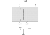
- FIG. 3 is a plan view of the optical coupler 1 as viewed in a first direction DIR1.
- FIG. 4 is a flowchart showing a method for manufacturing the optical coupler 1.
- FIG. 5 is a cross-sectional view of the optical coupler 1 during manufacturing.
- FIG. 6 is a diagram showing a pixel 15 of the grayscale mask 10.
- FIG. 7 is a diagram showing a pattern in which the pixels 15 of the grayscale mask 10 are arranged in order of aperture ratio.
- FIG. 8 shows an example of a grayscale mask 10 corresponding to the optical coupler 1 .
- FIG. 1 is a perspective view of an optical coupler 1.
- FIG. 2 is a cross-sectional view of the optical coupler 1 and the optical fiber 5 .
- FIG. 3 is a plan view of the optical coupler 1 as viewed in a
- FIG. 9 shows a light intensity distribution in a comparative example during an exposure process.
- FIG. 10 shows the light intensity distribution in the exposure process according to the first embodiment.
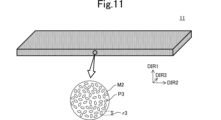
- FIG. 11 is a perspective view of the light-transmitting substrate 11.
- FIG. 12 is a cross-sectional view of the optical coupler 1 b and the optical fiber 5 .
- FIG. 13 is a flowchart showing a method for manufacturing the optical coupler 1b.
- FIG. 14 is a cross-sectional view of the optical coupler 1b during manufacturing.
- FIG. 15 is a cross-sectional view of the optical coupler 1c and the optical fiber 5.
- FIG. 16 is a cross-sectional view of the optical coupler 1c during manufacturing.
- FIG. 17 is a cross-sectional view of the optical coupler 1d and the optical fiber 5.
- FIG. 18 is a perspective view of the photoelectric conversion circuit module 50 and the optical fiber 5 .
- FIG. 19 is a cross-sectional view of the photoelectric conversion circuit module 50 and the optical fiber 5 taken along the line AA.
- FIG. 20 is a perspective view of the photoelectric conversion circuit module 50 a and the optical fiber 5 .
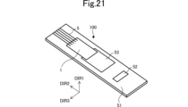
- FIG. 21 is a perspective view of the optical transceiver 100 and the optical fiber 5 .
- Fig. 1 is a perspective view of the optical coupler 1.
- Fig. 2 is a cross-sectional view of the optical coupler 1 and an optical fiber 5.
- Fig. 3 is a plan view of the optical coupler 1 as viewed in a first direction DIR1.
- directions are defined as follows. As shown in FIG. 1, the direction in which the bottom 24 and the reflecting portion 3 are arranged in this order is defined as the first direction DIR1. The direction in which the reflecting portion 3 and the optical fiber fixing portion 4 are arranged in this order is defined as the second direction DIR2. The direction in which the second side wall portion 22 and the third side wall portion 23 are arranged in this order is defined as the third direction DIR3. The first direction DIR1, the second direction DIR2, and the third direction DIR3 are mutually perpendicular.
- first direction DIR1, the second direction DIR2, and the third direction DIR3 in this specification are directions defined for the convenience of explanation, and do not have to coincide with the first direction DIR1, the second direction DIR2, and the third direction DIR3 when the optical coupler 1 is in use.
- the optical coupler 1 is a device for changing the direction of light emitted from a photoelectric conversion circuit or the like and outputting it to an optical fiber, or for changing the direction of light emitted from an optical fiber and outputting it to a photoelectric conversion circuit or the like.
- the optical coupler 1 changes the direction of light L emitted from a photoelectric conversion circuit or the like from a first direction DIR1 to a second direction DIR2 and outputs it to an optical fiber 5.
- the optical coupler 1 has an incident surface S11 that makes the light L incident in the first direction DIR1 and an output surface S12 that outputs the light L in the second direction DIR2.
- optical coupler 1 changes the direction of light L emitted from the optical fiber 5 from the opposite direction of the second direction DIR2 to the opposite direction of the first direction DIR1 and outputs it to a photoelectric conversion circuit or the like, the incident surface and the output surface may be interchanged.
- the optical coupler 1 is an example of an "optical coupler" of the present invention.
- the "optical coupler” of the present invention may be a focusing lens or a microlens array. The structure of the optical coupler 1 will be described in detail below.
- the optical coupler 1 includes a holding portion 2, a reflecting portion 3, and an optical fiber fixing portion 4.
- the optical coupler 1 is integrally molded from glass containing a filler.
- the optical coupler 1 is also a single member.
- a single member means a member that has a structure that cannot be separated without being damaged. Therefore, for example, a member in which two resin pieces are fixed with a screw is not a single member.
- the optical coupler 1 does not have to be integrally molded from glass containing a filler.
- the optical coupler 1 does not have to be a single member.
- the optical coupler 1 is integrally molded from a material including glass M1 and a plurality of first fillers P1 mixed in the glass M1.
- Glass is an amorphous material that exhibits a glass transition phenomenon.
- the glass include simple oxide glasses such as SiO 2 , B 2 O 3 , P 2 O 5 , GeO 2 , and AS3O 3 ; silicate glasses such as Li 2 O-SiO 2 , Na 2 O-SiO 2 , and K 2 O-SiO 2 ; aluminosilicate glasses such as Na 2 O-Al 2 O 3 -SiO 2 and CaO-Al 2 O 3 -SiO 2 ; borate glasses such as Li 2 O-B 2 O 3 and Na 2 O-B 2 O 3 ; aluminoborate glasses such as CaO-Al 2 O 3 -B 2 O 3 ; and borosilicate glasses such as Na 2 O-Al 2 O 3 -B 2 O 3 -SiO 2 .
- the multiple first fillers P1 are metal oxide particles such as crystalline silica, amorphous silica, alumina, magnesium oxide, titanium oxide, barium titanate, calcium titanate, etc., or organic particles such as graphite.
- the first filler P1 contains fillers having a non-spherical shape.
- the multiple first fillers P1 are dispersed throughout the glass M1. Note that the first filler P1 does not have to contain fillers having a non-spherical shape.
- the multiple first fillers P1 may be uniformly dispersed throughout the glass M1, or may be non-uniformly dispersed throughout the glass M1.
- the longest length of each of the multiple first fillers P1 is r1. If each of the multiple first fillers P1 has a spherical shape, the longest length r1 of each of the multiple first fillers P1 is the diameter of the sphere. If each of the multiple first fillers P1 has an elliptical spherical shape, the longest length r1 of each of the multiple first fillers P1 is the length in the major axis direction of the elliptical sphere. In this way, the longest length r1 of each of the multiple first fillers P1 is the longitudinal length of the longest part of each of the multiple first fillers P1.
- the maximum value of the longest length r1 of each of the multiple first fillers P1 is longer than the wavelength ⁇ of ultraviolet light UV, which will be described later.
- the holding portion 2 holds each of the reflecting portion 3 and the optical fiber fixing portion 4.
- the holding portion 2 is connected to each of the reflecting portion 3 and the optical fiber fixing portion 4.
- the holding portion 2 includes a first side wall portion 21, a second side wall portion 22, a third side wall portion 23, and a bottom portion 24. Note that the holding portion 2 does not necessarily have to include each of the first side wall portion 21, the second side wall portion 22, and the third side wall portion 23.
- the first side wall portion 21 is connected to each of the second side wall portion 22, the third side wall portion 23, and the bottom portion 24. More specifically, the first side wall portion 21 has a shape extending in the third direction DIR3. In this embodiment, the first side wall portion 21 has a plate shape. The end face of the first side wall portion 21 in the third direction DIR3 is connected to the third side wall portion 23. The end face of the first side wall portion 21 in the opposite direction to the third direction DIR3 is connected to the second side wall portion 22. The end face of the first side wall portion 21 in the opposite direction to the first direction DIR1 is connected to the bottom portion 24. Note that the first side wall portion 21 does not have to have a plate shape.
- the second side wall portion 22 is connected to each of the first side wall portion 21, the bottom portion 24, the reflecting portion 3, and the optical fiber fixing portion 4. More specifically, the second side wall portion 22 has a shape extending in the second direction DIR2. In this embodiment, the second side wall portion 22 has a plate shape. A portion of the end face of the second side wall portion 22 in the third direction DIR3 is connected to each of the end face of the first side wall portion 21 in the opposite direction to the third direction DIR3, the reflecting portion 3, and the optical fiber fixing portion 4. The end face of the second side wall portion 22 in the opposite direction to the first direction DIR1 is connected to the bottom portion 24. Note that the second side wall portion 22 does not have to have a plate shape.
- the third side wall portion 23 is connected to each of the first side wall portion 21, the bottom portion 24, the reflecting portion 3, and the optical fiber fixing portion 4. More specifically, the third side wall portion 23 has a shape extending in the second direction DIR2. In this embodiment, the third side wall portion 23 has a plate shape. A portion of the end face of the third side wall portion 23 in the opposite direction to the third direction DIR3 is connected to each of the end face of the first side wall portion 21 in the third direction DIR3, the reflecting portion 3, and the optical fiber fixing portion 4. The end face of the third side wall portion 23 in the opposite direction to the first direction DIR1 is connected to the bottom portion 24. Note that the third side wall portion 23 does not have to have a plate shape.
- the bottom 24 is connected to each of the first side wall 21, the second side wall 22, the third side wall 23, the reflector 3, and the optical fiber fixing part 4. More specifically, the bottom 24 has a plate shape. In this embodiment, the bottom 24 has a rectangular shape when viewed in the first direction DIR1. A portion of the end face of the bottom 24 in the first direction DIR1 is connected to each of the end face of the first side wall 21 in the opposite direction to the first direction DIR1, the end face of the second side wall 22 in the opposite direction to the first direction DIR1, the end face of the third side wall 23 in the opposite direction to the first direction DIR1, the reflector 3, and the optical fiber fixing part 4. Note that the bottom 24 does not have to have a rectangular shape when viewed in the first direction DIR1.
- light L enters the optical coupler 1 from end face S1 of the bottom 24 in the opposite direction to the first direction DIR1. Therefore, end face S1 of the bottom 24 in the opposite direction to the first direction DIR1 includes the incident surface S11 of the optical coupler 1. Light L that enters the bottom 24 from end face S1 of the bottom 24 in the opposite direction to the first direction DIR1 passes through the inside of the bottom 24 and enters the reflector 3.
- the area that overlaps with the reflecting portion 3 when viewed in the first direction DIR1 is defined as area A1.
- area A2 the area that does not overlap with the reflecting portion 3 when viewed in the first direction DIR1 is defined as area A2.
- the end face S1 of the bottom 24 in the opposite direction to the first direction DIR1 includes both area A1 and area A2. Light L is incident on the optical coupler 1 from area A1 of the bottom 24. Therefore, area A1 is the incident surface S11.
- Area A2 is the mounting surface S21 for mounting the optical coupler 1 on a substrate when the optical coupler 1 is incorporated into an optoelectric conversion circuit module or the like.
- the end surface S1 of the bottom 24 in the opposite direction to the first direction DIR1 includes an incident surface S11 and a mounting surface S21. That is, the mounting surface S21 is in the same plane as the incident surface S11.
- the reflecting portion 3 is connected to each of the second side wall portion 22, the third side wall portion 23, and the bottom portion 24. As shown in FIG. 2, the reflecting portion 3 changes the traveling direction of the light L incident on the incident surface S11 from the first direction DIR1 to the second direction DIR2, and outputs the light to one of the five optical fibers 5.
- the reflecting portion 3 includes a prism portion 31 and five focusing lens portions 32. The number of focusing lens portions 32 is not limited to five. Furthermore, the reflecting portion 3 does not have to include a focusing lens portion 32.
- the prism portion 31 is connected to each of the second side wall portion 22, the third side wall portion 23, and the bottom portion 24. More specifically, in this embodiment, the prism portion 31 has a right-angled isosceles triangular prism shape extending in the third direction DIR3.
- the prism portion 31 has a prism portion entrance surface S2, a prism portion reflection surface S3, a prism portion exit surface S4, an end face in the third direction DIR3, and an end face in the opposite direction to the third direction DIR3.
- the end face of the prism portion 31 in the third direction DIR3 is connected to the third side wall portion 23.
- the end face of the prism portion 31 in the opposite direction to the third direction DIR3 is connected to the second side wall portion 22. Note that the prism portion 31 does not have to have a right-angled isosceles triangular prism shape.
- the prism portion entrance surface S2 is the end surface of the prism portion 31 in the opposite direction to the first direction DIR1.
- the prism portion entrance surface S2 is connected to the bottom portion 24.
- Light L that passes through the inside of the bottom portion 24 enters the prism portion 31 from the prism portion entrance surface S2.
- Light L that enters the prism portion 31 from the prism portion entrance surface S2 passes through the inside of the prism portion 31.
- the prism portion reflective surface S3 When viewed in the third direction DIR3, the prism portion reflective surface S3 forms an angle of 45 degrees with each of the prism portion entrance surface S2 and the prism portion exit surface S4.
- the end of the prism portion reflective surface S3 in the first direction DIR1 is located in the second direction DIR2 from the end of the prism portion reflective surface S3 in the opposite direction to the first direction DIR1.
- the prism portion reflective surface S3 reflects the light L that has passed through the inside of the prism portion 31. As a result, the prism portion reflective surface S3 changes the traveling direction of the light L from the first direction DIR1 to the second direction DIR2.
- the focusing lens sections 32 are provided on the prism section reflecting surface S3.
- the five focusing lens sections 32 are lined up in the third direction DIR3.
- the surfaces of the focusing lens sections 32 are aspheric.
- the focusing lens sections 32 reflect the light L that passes through the inside of the prism section 31 and whose traveling direction vector includes a component of the first direction DIR1 while focusing the light L. As a result, the focusing lens sections 32 change the traveling direction of the light L from a direction including a component of the first direction DIR1 to the second direction DIR2.
- the prism section exit surface S4 is the end surface of the prism section 31 in the first direction DIR1.
- the prism section exit surface S4 is perpendicular to the prism section entrance surface S2.
- the prism section exit surface S4 emits light L that has been reflected by the prism section reflecting surface S3 or the focusing lens section 32 and passed through the inside of the prism section 31.
- the light L emitted from the prism section exit surface S4 travels in the first direction DIR1.
- the prism section exit surface S4 is the exit surface S12 of the optical coupler 1.
- the optical fiber fixing portion 4 fixes each of the five optical fibers 5.
- the optical fiber fixing portion 4 is connected to each of the second side wall portion 22, the third side wall portion 23, and the bottom portion 24. More specifically, the optical fiber fixing portion 4 has a plate shape extending in the third direction DIR3.
- the end face of the optical fiber fixing portion 4 in the third direction DIR3 is connected to the third side wall portion 23.
- the end face of the optical fiber fixing portion 4 in the opposite direction to the third direction DIR3 is connected to the second side wall portion 22.
- the end face of the optical fiber fixing portion 4 in the opposite direction to the first direction DIR1 is connected to the bottom portion 24.
- each of the five grooves G has a shape extending in the second direction DIR2.
- the five grooves G are aligned in the third direction DIR3.
- five optical fibers 5 are fixed to each of the five grooves G.
- the five optical fibers 5 are aligned in the third direction DIR3.
- Each of the five optical fibers 5 and the five focusing lens parts 32 are aligned in the second direction DIR2 when viewed in the first direction DIR1.
- grooves G may not be provided on the end face of the optical fiber fixing part 4 in the first direction DIR1.
- each of the five grooves G may have a U-shape when viewed in the second direction DIR2.
- the number of grooves G is not limited to five.
- Each of the five optical fibers 5 has a shape that extends in the second direction DIR2.
- the end face of each of the five optical fibers 5 facing the opposite direction of the second direction DIR2 faces the opposite direction of the second direction DIR2.
- the end face of each of the five optical fibers 5 facing the opposite direction of the second direction DIR2 faces the prism section exit surface S4 with a gap between them. As a result, the light L emitted from the prism section exit surface S4 is incident on one of the five optical fibers 5.
- Fig. 4 is a flowchart showing the method for manufacturing the optical coupler 1.
- Fig. 5 is a cross-sectional view of the optical coupler 1 during manufacturing. Note that the second side wall portion 22 and the third side wall portion 23 are omitted in Fig. 5.
- Fig. 6 is a diagram showing pixels 15 of a grayscale mask 10.
- Fig. 7 is a diagram showing a pattern in which the pixels 15 of the grayscale mask 10 are arranged in order of aperture ratio.
- Fig. 8 is an example of a grayscale mask 10 corresponding to the optical coupler 1.
- a light-transmitting substrate 11 is prepared having a first main surface SU11 and a second main surface SU12 aligned in a first direction DIR1 (preparation process, FIG. 4: step ST1).
- the first main surface SU11 is located in the first direction DIR1 from the second main surface SU12.
- the light-transmitting substrate 11 has a plate shape.
- the first photosensitive glass paste 12 is applied to the first main surface SU11 of the light-transmitting substrate 11 (first application step, FIG. 4: step ST2).
- the first photosensitive glass paste 12 is negative type.
- the first photosensitive glass paste 12 may be positive type.
- the solubility of the exposed portion in the developer increases.
- the unexposed portion of the first photosensitive glass paste 12 remains.
- the first photosensitive glass paste 12 includes glass M1 and a plurality of first fillers P1 mixed in the glass M1.
- the first photosensitive glass paste 12 may include additives such as a dispersant and a light absorber in addition to the glass M1 and the plurality of first fillers P1 mixed in the glass M1.
- a grayscale mask 10 is placed on the second main surface SU12 of the light-transmitting substrate 11 (mask process, FIG. 4: step ST3).
- the grayscale mask 10 is formed in a binary pattern.
- the grayscale mask 10 adjusts the light transmittance by controlling the aperture ratio.
- the grayscale mask 10 will be described in detail below.
- the grayscale mask 10 is configured with multiple pixels 15 arranged adjacent to each other.
- the pixel 15 has a unit area 16 and a runner portion 17.
- the unit area 16 is square-shaped when viewed in the first direction DIR1.
- the unit area 16 is further divided into four square-shaped portions A11, A12, A21, and A22.
- the runner portion 17 is arranged around the unit area 16 when viewed in the first direction DIR1.
- the runner portion 17 is a light-shielding area b that does not transmit light.
- the unit area 16 is composed of an open light-transmitting area a (which allows light to pass through) and a closed light-shielding area b (which does not allow light to pass through).
- the opening ratio (light transmittance) of the unit area 16 changes as the area ratio between the light-transmitting area a and the light-shielding area b changes.
- the aperture ratio of the unit region 16 is 100%.
- the area ratio of the light-transmitting region a to the light-shielding region b is 1:1, and the aperture ratio (light transmittance) of the unit region 16 is 50%.
- the aperture ratio of the unit region 16 is 0%.
- the pattern on the grayscale mask 10 forms a gradation.
- unit regions 16 with aperture ratios differing by 10% are arranged in order, but by increasing the resolution of the aperture ratio, for example by arranging unit regions 16 with aperture ratios differing by 0.1%, the continuity of the light transmittance can be maintained. In this way, the grayscale mask 10 adjusts the light transmittance by controlling the aperture ratio.
- the optical coupler 1 can be manufactured using the grayscale mask 10 by increasing the aperture ratio of the portions of the grayscale mask 10 corresponding to the first side wall portion 21, the second side wall portion 22, and the third side wall portion 23 and decreasing the aperture ratio of the portions of the grayscale mask 10 corresponding to the groove G.
- ultraviolet rays UV are irradiated onto the second main surface SU12 of the light-transmitting substrate 11 to expose the first photosensitive glass paste 12 (exposure process, FIG. 4: step ST4).
- the wavelength ⁇ of the ultraviolet rays UV is longer than 10 nm and shorter than 380 nm.
- the exposure process exposes the first photosensitive glass paste 12 to light.
- the maximum value of the longest length r1 of each of the multiple first fillers P1 is longer than the wavelength ⁇ of the ultraviolet rays UV.
- the grayscale mask 10 is removed from the second main surface SU12 of the light-transmitting substrate 11, and the first photosensitive glass paste 12 is developed (developing step, FIG. 4: step ST5). More specifically, the first photosensitive glass paste 12 and the light-transmitting substrate 11 are immersed in a developer. By the developing step, the exposed portions of the first photosensitive glass paste 12 remain, and the unexposed portions are removed. After development, the first photosensitive glass paste 12 and the light-transmitting substrate 11 are washed and dried.
- the translucent substrate 11 is removed from the developed first photosensitive glass paste 12, and the first photosensitive glass paste 12 is hardened (hardening process, FIG. 4: step ST6). More specifically, the first photosensitive glass paste 12 is fired to harden the first photosensitive glass paste 12.
- the optical coupler 1 is completed. Note that, as shown in FIG. 5, grayscale masks 10 corresponding to multiple optical couplers 1 may be placed on the second main surface SU12 of the translucent substrate 11, and after the first photosensitive glass paste 12 hardens, the hardened first photosensitive glass paste 12 may be cut to complete multiple optical couplers 1.
- FIG. 9 shows the light intensity distribution of the comparative example in the exposure process.
- FIG. 10 shows the light intensity distribution of the first embodiment in the exposure process.
- the ultraviolet light UV is a laser light.
- the beam diameter of the ultraviolet light UV is sufficiently smaller than the light transmission region a.
- the ultraviolet light UV is diffracted by the periodic structure of the light-transmitting regions a and light-shielding regions b of the grayscale mask 10.
- the first photosensitive glass paste 12 does not contain filler, as shown in FIG. 9, a high level of light is distributed in positions other than the position x1 in the second direction DIR2 of the ultraviolet light UV. Therefore, the first photosensitive glass paste 12 is exposed to a high level of ultraviolet light UV in positions other than the position x1.
- the first photosensitive glass paste 12 is negative type. Therefore, in the development process, the first photosensitive glass paste 12 is likely to remain in positions other than the position x1. In this way, light distributed in positions other than the position x1 causes a decrease in processing accuracy.
- the first photosensitive glass paste 12 contains the first filler P1.
- the longest length r1 of the first filler P1 is longer than the wavelength ⁇ of the ultraviolet ray UV.
- the ultraviolet ray UV diffracted by the periodic structure of the light transmitting region a and the light blocking region b of the grayscale mask 10 is scattered by the first filler P1.
- the light intensity distribution of the ultraviolet ray UV becomes a normal distribution that is strongest at the position x1, and the light intensity I(x) distributed other than the position x1 is smaller than that of the comparative example as shown in FIG. 10, and a high level of the ultraviolet ray UV is not irradiated other than the position x1. Therefore, in the development process, the first photosensitive glass paste 12 is less likely to remain at the position other than the position x1.
- the maximum length r1 of the first filler P1 is equal to or less than the wavelength ⁇ of the ultraviolet ray UV, scattering of the ultraviolet ray UV is suppressed. Therefore, when using a grayscale mask 10 formed in a binary pattern, scattering of the ultraviolet ray UV occurs by making the maximum length r1 of the first filler P1 longer than the wavelength ⁇ of the ultraviolet ray UV, and it is possible to reduce the light intensity I(x) distributed in positions other than the position x1 in the second direction DIR2 of the ultraviolet ray UV.
- the content of the first filler P1 contained in the first photosensitive glass paste 12 can be reduced. More specifically, the first filler P1 contains fillers having a non-spherical shape. This allows more scattering of ultraviolet light UV to occur compared to when the first filler P1 contains only fillers having a spherical shape. As a result, according to the manufacturing method of the optical coupler 1, the content of the first filler P1 contained in the first photosensitive glass paste 12 can be reduced.
- the longest length r1 of each of the multiple first fillers P1 is smaller than the wavelength ⁇ of ultraviolet light UV. Note that in this modified example, the longest length r1 of each of the multiple first fillers P1 may be greater than or equal to the wavelength ⁇ of ultraviolet light UV. Also, in this modified example, the optical coupler 1a may not include the first filler P1. Note that in this modified example, the optical coupler 1a corresponds to the "first glass portion" of the present invention.
- Fig. 11 is a perspective view of the light-transmitting substrate 11.
- Fig. 11 only a representative third filler P3 among the multiple third fillers P3 is given a reference symbol.
- the method for manufacturing the optical coupler 1a according to the first modified example only the parts that are different from the method for manufacturing the optical coupler 1 according to the first embodiment will be described, and the rest will be omitted.
- the light-transmitting substrate 11 includes a medium M2 and a plurality of third fillers P3 mixed into the medium M2.
- the medium M2 is, for example, a resin.
- the medium M2 may also be glass or the like.
- the multiple third fillers P3 are metal oxide particles such as crystalline silica, amorphous silica, alumina, magnesium oxide, titanium oxide, barium titanate, calcium titanate, etc., or organic particles such as graphite.
- the third filler P3 contains fillers having a non-spherical shape.
- the multiple third fillers P3 are dispersed throughout the medium M2. Note that the third filler P3 does not have to contain fillers having a non-spherical shape.
- the multiple third fillers P3 may be uniformly dispersed throughout the medium M2, or may be non-uniformly dispersed throughout the medium M2.
- the maximum length of each of the multiple third fillers P3 is r3. If each of the multiple third fillers P3 has a spherical shape, the maximum length r3 of each of the multiple third fillers P3 is the diameter of the sphere. If each of the multiple third fillers P3 has an elliptical spherical shape, the maximum length r3 of each of the multiple third fillers P3 is the length in the major axis direction of the elliptical sphere. In this way, the maximum length r3 of each of the multiple third fillers P3 is the longitudinal length of the longest part of each of the multiple third fillers P3.
- the maximum value of the maximum length r3 of each of the multiple third fillers P3 is longer than the wavelength ⁇ of ultraviolet light UV. Therefore, the maximum value of the maximum length r3 of each of the multiple third fillers P3 is longer than the maximum value of the maximum length r1 of each of the multiple first fillers P1.
- the light-transmitting substrate 11 does not need to be removed from the developed first photosensitive glass paste 12 during the curing process.
- the light-transmitting substrate 11 may be connected to the optical coupler 1a.
- the light-transmitting substrate 11 corresponds to the "transmitting portion" of the present invention.
- the above-described manufacturing method of the optical coupler 1a also has the same effect as the manufacturing method of the optical coupler 1.
- the content of the first filler P1 contained in the first photosensitive glass paste 12 can be reduced. More specifically, the longest length r3 of the third filler P3 contained in the light-transmitting substrate 11 is longer than the wavelength ⁇ of the ultraviolet ray UV. As a result, the ultraviolet ray UV diffracted by the periodic structure of the light-transmitting region a and the light-shielding region b of the grayscale mask 10 is scattered by the third filler P3 contained in the light-transmitting substrate 11.
- the light intensity distribution of the ultraviolet ray UV becomes a normal distribution that is strongest at the position x1, and the light intensity I(x) distributed other than the position x1 becomes smaller than that of the comparative example, and a high level of ultraviolet ray UV is not irradiated other than the position x1. Therefore, in the development process, the first photosensitive glass paste 12 is less likely to remain at the positions other than the position x1. This makes it possible to suppress a decrease in processing accuracy even if the content of the first filler P1 contained in the first photosensitive glass paste 12 is reduced. As a result, according to the manufacturing method of the optical coupler 1a, the content of the first filler P1 contained in the first photosensitive glass paste 12 can be reduced.
- the processing accuracy of the optical coupler 1a can be improved.
- the third filler P3 contains filler having a non-spherical shape. This allows more scattering of ultraviolet light UV compared to when the third filler P3 contains only filler having a spherical shape. Therefore, according to the manufacturing method of the optical coupler 1a, the content of the third filler P3 contained in the light-transmitting substrate 11 can be reduced. As a result, according to the manufacturing method of the optical coupler 1a, the processing accuracy of the optical coupler 1a can be improved.
- FIG. 12 is a cross-sectional view of the optical coupler 1b and the optical fiber 5. Note that the second side wall portion 22 and the third side wall portion 23 are omitted in Fig. 12. Note that, regarding the structure of the optical coupler 1b according to the second modified example, only the parts that are different from the structure of the optical coupler 1 according to the first embodiment will be described, and the rest will be omitted.
- the bottom 24 contains a plurality of first fillers P1, and the first side wall 21, the second side wall 22, the third side wall 23, the reflector 3, and the optical fiber fixing part 4 do not contain any filler.
- the bottom 24 contains a plurality of first fillers P1 only on the end face S1 of the bottom 24 in the opposite direction to the first direction DIR1, and no filler may be contained in any part other than the end face S1 of the bottom 24 in the opposite direction to the first direction DIR1.
- the bottom 24 corresponds to the "first glass part" of the present invention.
- the first side wall 21, the second side wall 22, the third side wall 23, the reflector 3, and the optical fiber fixing part 4 each correspond to the "second glass part” or the "transmitting part” of the present invention.
- the "second glass part” of the present invention contains at least glass.
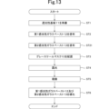
- Fig. 13 is a flowchart showing the method for manufacturing the optical coupler 1b.
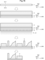
- Fig. 14 is a cross-sectional view of the optical coupler 1b during manufacturing. Note that the second side wall portion 22 and the third side wall portion 23 are omitted in Fig. 14. Note that, with regard to the method for manufacturing the optical coupler 1b according to the second modified example, only the parts that are different from the method for manufacturing the optical coupler 1 according to the first embodiment will be described, and the rest will be omitted.
- a second photosensitive glass paste 13 not containing a filler is applied to the first photosensitive glass paste 12 (second application step, FIG. 13: step ST21).
- the second photosensitive glass paste 13 is negative type. If the first photosensitive glass paste 12 is positive type, the second photosensitive glass paste 13 may be positive type.
- the second photosensitive glass paste 13 may contain additives such as a dispersant and a light absorber in addition to glass.
- the second application step may be performed after the mask step.
- the second application step may be performed between the first application step and the exposure step.
- ultraviolet rays UV are irradiated onto the second main surface SU12 of the light-transmitting substrate 11, exposing the first photosensitive glass paste 12 and the second photosensitive glass paste 13 (FIG. 13: step ST4).
- the exposure process exposes the first photosensitive glass paste 12 and the second photosensitive glass paste 13 to light.
- the grayscale mask 10 is removed from the second main surface SU12 of the light-transmitting substrate 11, and the first photosensitive glass paste 12 and the second photosensitive glass paste 13 are developed (FIG. 13: step ST5). More specifically, the first photosensitive glass paste 12, the second photosensitive glass paste 13, and the light-transmitting substrate 11 are immersed in a developer. In the development process, the exposed portions of the first photosensitive glass paste 12 and the second photosensitive glass paste 13 remain, and the unexposed portions are removed. After development, the first photosensitive glass paste 12, the second photosensitive glass paste 13, and the light-transmitting substrate 11 are washed and dried.
- the translucent substrate 11 is removed from the developed first photosensitive glass paste 12, and the first photosensitive glass paste 12 and the second photosensitive glass paste 13 are cured (FIG. 13: step ST6). More specifically, the first photosensitive glass paste 12 and the second photosensitive glass paste 13 are fired to harden the first photosensitive glass paste 12 and the second photosensitive glass paste 13.
- the above-described manufacturing method of the optical coupler 1b also has the same effect as the manufacturing method of the optical coupler 1. More specifically, in the exposure process, the ultraviolet rays UV are irradiated onto the second main surface SU12 of the light-transmitting substrate 11. Therefore, since the longest length r1 of the first filler P1 contained in the first photosensitive glass paste 12 applied to the first main surface SU11 of the light-transmitting substrate 11 is longer than the wavelength ⁇ of the ultraviolet rays UV, the ultraviolet rays UV diffracted by the periodic structure of the light-transmitting region a and the light-shielding region b of the grayscale mask 10 are scattered by the first filler P1.
- the light intensity distribution of the ultraviolet rays UV becomes a normal distribution that is strongest at position x1, and the light intensity I(x) distributed other than at position x1 is smaller than that of the comparative example, and a high level of ultraviolet rays UV is not irradiated other than at position x1. Therefore, in the development process, the first photosensitive glass paste 12 and the second photosensitive glass paste 13 are less likely to remain at positions other than position x1. Therefore, even if the second photosensitive glass paste 13 applied to the first photosensitive glass paste 12 does not contain a filler, the same effect as the manufacturing method of the optical coupler 1 can be achieved.
- the second photosensitive glass paste 13 does not contain a filler. Therefore, according to the manufacturing method of the optical coupler 1b, it is possible to improve the shape accuracy of the optical coupler 1b.
- FIG. 15 is a cross-sectional view of the optical coupler 1c and the optical fiber 5. Note that the second side wall portion 22 and the third side wall portion 23 are omitted in Fig. 15. Note that, regarding the structure of the optical coupler 1c according to the third modified example, only the parts that differ from the structure of the optical coupler 1b according to the second modified example will be described, and the rest will be omitted.
- the bottom 24 contains glass M1 and a plurality of first fillers P1 mixed into the glass M1.
- Each of the first side wall 21, the second side wall 22, the third side wall 23, the reflector 3, and the optical fiber fixing part 4 contains glass M1 and a plurality of second fillers P2 mixed into the glass M1.
- the content of the second filler P2 contained in each of the first side wall 21, the second side wall 22, the third side wall 23, the reflector 3, and the optical fiber fixing part 4 is lower than the content of the first filler P1 contained in the bottom 24.
- the content of the second filler P2 contained in the part other than the end face S1 in the opposite direction of the first direction DIR1 of the bottom 24 may be lower than the content of the first filler P1 contained in the end face S1 in the opposite direction of the first direction DIR1 of the bottom 24.
- the second fillers P2 are metal oxide particles such as crystalline silica, amorphous silica, alumina, magnesium oxide, titanium oxide, barium titanate, calcium titanate, etc., or organic particles such as graphite.
- the second fillers P2 contain fillers having a non-spherical shape.
- the second fillers P2 are dispersed throughout the glass M1.
- the second fillers P2 do not have to contain fillers having a non-spherical shape.
- the second fillers P2 may be uniformly dispersed throughout the glass M1, or may be non-uniformly dispersed throughout the glass M1.
- Fig. 16 is a cross-sectional view of the optical coupler 1c during manufacturing. Note that the second side wall portion 22 and the third side wall portion 23 are omitted in Fig. 16. Note that, regarding the method for manufacturing the optical coupler 1c according to the third modified example, only the parts that are different from the method for manufacturing the optical coupler 1b according to the second modified example will be described, and the rest will be omitted.
- a second photosensitive glass paste 13 containing a second filler P2 is applied to the first photosensitive glass paste 12 (second application step).
- the content of the second filler P2 contained in the second photosensitive glass paste 13 is lower than the content of the first filler P1 contained in the first photosensitive glass paste 12.
- the second application step may be performed after the mask step.
- the second application step may be performed between the first application step and the exposure step.
- the above-described method for manufacturing the optical coupler 1c also provides the same effect as the method for manufacturing the optical coupler 1b. More specifically, for the same reason as the method for manufacturing the optical coupler 1b, even if the content of the second filler P2 contained in the second photosensitive glass paste 13 applied to the first photosensitive glass paste 12 is lower than the content of the first filler P1 contained in the first photosensitive glass paste 12, the same effect as the method for manufacturing the optical coupler 1b is provided.
- the content of the second filler P2 contained in the second photosensitive glass paste 13 is lower than the content of the first filler P1 contained in the first photosensitive glass paste 12. Therefore, according to the manufacturing method of the optical coupler 1c, it is possible to improve the shape accuracy of the optical coupler 1c.
- FIG. 17 is a cross-sectional view of the optical coupler 1d and the optical fiber 5. Note that the second side wall 22 and the third side wall 23 are omitted in Fig. 17. Note that, regarding the structure of the optical coupler 1d according to the fourth modified example, only the parts that differ from the structure of the optical coupler 1c according to the third modified example will be described, and the rest will be omitted.
- the maximum length of each of the multiple second fillers P2 is r2. If each of the multiple second fillers P2 has a spherical shape, the maximum length r2 of each of the multiple second fillers P2 is the diameter of the sphere. If each of the multiple second fillers P2 has an elliptical spherical shape, the maximum length r2 of each of the multiple second fillers P2 is the length in the major axis direction of the elliptical sphere. In this way, the maximum length r2 of each of the multiple second fillers P2 is the longitudinal length of the longest part of each of the multiple second fillers P2.
- the maximum value of the maximum length r2 of each of the multiple second fillers P2 is longer than 0 and is equal to or less than the wavelength ⁇ of ultraviolet light UV. Therefore, the maximum value of the maximum length r2 of each of the multiple second fillers P2 is shorter than the maximum value of the maximum length r1 of each of the multiple first fillers P1.
- the maximum value of the longest length r2 of each of the multiple second fillers P2 is different from the maximum value of the longest length r1 of each of the multiple first fillers P1.
- the maximum value of the longest length r2 of each of the multiple second fillers P2 contained in the second photosensitive glass paste 13 is longer than 0 and is equal to or less than the wavelength ⁇ of ultraviolet light UV.
- the above-described method for manufacturing the optical coupler 1d also provides the same effects as the method for manufacturing the optical coupler 1c. More specifically, for the same reasons as the method for manufacturing the optical coupler 1c, even if the longest length r2 of the second filler P2 contained in the second photosensitive glass paste 13 applied to the first photosensitive glass paste 12 is longer than 0 and is equal to or less than the wavelength ⁇ of ultraviolet light UV, the same effects as the method for manufacturing the optical coupler 1c are provided.
- the longest length r2 of the second filler P2 contained in the second photosensitive glass paste 13 is longer than 0 and is equal to or less than the wavelength ⁇ of the ultraviolet light UV. Therefore, according to the manufacturing method of the optical coupler 1d, the processing accuracy of the optical coupler 1d can be improved.
- FIG. 18 is a perspective view of the photoelectric conversion circuit module 50 and the optical fiber 5.
- reference symbols are given only to representative optical couplers 1, optical fibers 5, and optical waveguides OW among the multiple optical couplers 1, multiple optical fibers 5, and multiple optical waveguides OW.
- Fig. 19 is a cross-sectional view of the photoelectric conversion circuit module 50 and the optical fiber 5 taken along the line A-A.
- the photoelectric conversion circuit module 50 includes a plurality of optical couplers 1, a substrate 51, and an optical conversion circuit 52.
- the plurality of optical couplers 1 and the optical conversion circuit 52 are mounted on the substrate 51.
- the optical conversion circuit 52 is disposed in the center of the substrate 51 when viewed in the first direction DIR1.
- the plurality of optical couplers 1 are disposed around the optical conversion circuit 52 when viewed in the first direction DIR1.
- Each of the plurality of optical fibers 5 is fixed to the optical fiber fixing portion 4 of each of the plurality of optical couplers 1.
- the number of optical couplers 1 is not limited to a plurality, and may be one.
- the optical conversion circuit 52 does not have to be disposed in the center of the substrate 51 when viewed in the first direction DIR1. Furthermore, the plurality of optical couplers 1 do not have to be disposed around the optical conversion circuit 52 when viewed in the first direction DIR1. Furthermore, the photoelectric conversion circuit module 50 may include an optical coupler 1a, an optical coupler 1b, an optical coupler 1c, or an optical coupler 1d instead of the optical coupler 1.
- the substrate 51 has a plate shape with two main surfaces aligned in the first direction DIR1. However, as shown in FIG. 19, an optical waveguide OW and a mirror M are provided inside the substrate 51.
- the optical waveguide OW is provided between the photoelectric conversion circuit 52 and each of the multiple optical couplers 1.
- the mirror M is provided in the opposite direction of the first direction DIR1 from the reflecting section 3. The light L emitted by the photoelectric conversion circuit 52 passes through the optical waveguide OW.
- the optical couplers 1 are mounted on one of the two main surfaces of the substrate 51, the main surface located in the first direction DIR1. More specifically, the mounting surface S21 is mounted on the main surface located in the first direction DIR1, the main surface of the substrate 51.
- the photoelectric conversion circuit 52 is mounted on the principal surface of the substrate 51 that is located in the first direction DIR1, out of the two principal surfaces.
- the photoelectric conversion circuit 52 converts an electrical signal into light that enters the optical coupler 1, or converts light emitted from the optical coupler 1 into an electrical signal. The following describes the case where the photoelectric conversion circuit 52 converts an electrical signal into light that enters the optical coupler 1.
- the photoelectric conversion circuit 52 converts the electrical signal into light L that is incident on each of the multiple optical couplers 1.
- the light L emitted by the photoelectric conversion circuit 52 travels in the second direction DIR2 through the optical waveguide OW.
- the light L traveling in the second direction DIR2 through the optical waveguide OW is reflected by the mirror M.
- the traveling direction of the light L is changed from the second direction DIR2 to the first direction DIR1.
- the light L then enters the incident surface S11 of the optical coupler 1, and the traveling direction is changed by the optical coupler 1 from the first direction DIR1 to the second direction DIR2, and is emitted from the exit surface S12 of the optical coupler 1.
- the light L is incident on each of the five optical fibers 5.
- the above-described photoelectric conversion circuit module 50 also provides the same effects as the optical coupler 1.
- FIG. 20 is a perspective view of the photoelectric conversion circuit module 50a and the optical fiber 5.
- reference symbols are given only to representative optical couplers 1 and optical fibers 5 among the plurality of optical couplers 1 and the plurality of optical fibers 5.
- the photoelectric conversion circuit module 50a according to the sixth modified example only the parts different from the photoelectric conversion circuit module 50 according to the fifth modified example will be described, and the rest will be omitted.
- the photoelectric conversion circuit module 50a differs from the photoelectric conversion circuit module 50 in that the substrate 51 is a semiconductor substrate and that the substrate 51 includes multiple light emitting sections 53.
- the number of light emitting sections 53 is not limited to multiple, and may be one.
- Each of the multiple light emitting sections 53 is, for example, a surface light emitting element formed on the main surface located in the first direction DIR1 of the two main surfaces of the substrate 51.
- Each of the multiple light emitting sections 53 is, for example, a VCSEL (Vertical Cavity Surface Emitting Laser).
- Each of the multiple light emitting sections 53 emits light L based on an electrical signal generated by the photoelectric conversion circuit 52. The light L emitted by each of the multiple light emitting sections 53 is incident on each of the multiple optical fibers 5 via each of the multiple optical couplers 1.
- the photoelectric conversion circuit module 50a described above also provides the same effects as the photoelectric conversion circuit module 50.
- Fig. 21 is a perspective view of the optical transceiver 100 and the optical fibers 5. In Fig. 21, only a representative optical fiber 5 out of the five optical fibers 5 is denoted by a reference symbol.
- the optical transceiver 100 according to the seventh modification only the parts that are different from the photoelectric conversion circuit module 50a according to the sixth modification will be described, and the rest will be omitted.
- the optical transceiver 100 differs from the photoelectric conversion circuit module 50a in that it has one optical coupler 1 and one light emitting section 53.
- the light L emitted by the light emitting unit 53 enters each of the five optical fibers 5 via the optical coupler 1, or the light L emitted from each of the five optical fibers 5 enters the photoelectric conversion circuit 52 via the optical coupler 1.
- the optical transceiver 100 described above also provides the same effects as the photoelectric conversion circuit module 50a.
- the optical coupler according to the present invention is not limited to the optical coupler 1, the optical coupler 1a, the optical coupler 1b, the optical coupler 1c, and the optical coupler 1d, and may be modified within the scope of the gist of the present invention.
- the structures of the optical coupler 1, the optical coupler 1a, the optical coupler 1b, the optical coupler 1c, and the optical coupler 1d may be arbitrarily combined.
- the photoelectric conversion circuit module according to the present invention is not limited to the photoelectric conversion circuit module 50 and the photoelectric conversion circuit module 50a, but can be modified within the scope of the gist.
- the structures of the photoelectric conversion circuit module 50 and the photoelectric conversion circuit module 50a may be combined in any manner.
- optical transceiver is not limited to the optical transceiver 100, but can be modified within the scope of the gist.
- the present invention has the following configuration.
- a second application step of applying a second photosensitive glass paste to the first photosensitive glass paste is provided between the first application step and the exposure step, In the exposure step, the first photosensitive glass paste and the second photosensitive glass paste are exposed to light, In the developing step, the first photosensitive glass paste and the second photosensitive glass paste are developed; In the curing step, the first photosensitive glass paste and the second photosensitive glass paste are cured; the second photosensitive glass paste includes a second filler, and a content of the second filler in the second photosensitive glass paste is lower than a content of the first filler in the first photosensitive glass paste; Alternatively, the second photosensitive glass paste does not include the second filler.
- the exposure step the first photosensitive glass paste and the second photosensitive glass paste are exposed to light
- the developing step the first photosensitive glass paste and the second photosensitive glass paste are developed
- the curing step the first photosensitive glass paste and the second photosensitive glass paste are cured;
- the longest length of the second filler is greater than 0 and is equal to or less than the wavelength of the ultraviolet light.
- the first filler includes a filler having a non-spherical shape.
- the third filler includes a filler having a non-spherical shape.
- a first glass portion including a first glass and a first filler mixed in the first glass
- a second glass portion including at least a second glass and connected to the first glass portion
- Equipped with the second glass portion includes a second filler mixed in the second glass, and a content of the second filler contained in the second glass portion is lower than a content of the first filler contained in the first glass portion;
- the second glass portion does not include the second filler.
- the transmission portion includes a medium and a second filler mixed in the medium, The maximum length of the second filler is different from the maximum length of the first filler.
- Optical coupler
- the medium is glass.
- the first filler includes a filler having a non-spherical shape.
- the transmission portion is a light-transmitting substrate.
- the second filler includes a filler having a non-spherical shape.
- An optical coupler according to any one of (7) to (13), A substrate; a photoelectric conversion circuit mounted on the substrate; The photoelectric conversion circuit converts an electrical signal into light incident on the optical coupler, or converts light emitted from the optical coupler into an electrical signal. Photoelectric conversion circuit module.
- the substrate is a semiconductor substrate and includes a light emitting portion that emits light
- the optical coupler is mounted on the substrate.
- Optical coupler 2 Holding section 3: Reflecting section 4: Optical fiber fixing section 5: Optical fiber 10: Grayscale mask 11: Light-transmitting substrate 12: First photosensitive glass paste 13: Second photosensitive glass paste 15: Pixel 16: Unit area 17: Runner section 21: First side wall section 22: Second side wall section 23: Third side wall section 24: Bottom section 31: Prism section 32: Condenser lens section 50, 50a: Photoelectric conversion circuit module 51: Substrate 52: Photoelectric conversion circuit 53: Light emitting section 100: Optical transceiver A1, A2: Areas A11, A12, A21, A22: Square-shaped portions DIR1: First direction DIR2: Second direction DIR3: Third direction G: Groove I: Light intensity L: Light M: Mirror M1: Glass M2: Medium OW: Optical waveguide P1: First filler P2: Second filler P3: Third filler S1: End face S11: Inc
Landscapes
- Physics & Mathematics (AREA)
- General Physics & Mathematics (AREA)
- Optics & Photonics (AREA)
- Optical Couplings Of Light Guides (AREA)
Priority Applications (3)
| Application Number | Priority Date | Filing Date | Title |
|---|---|---|---|
| JP2024549672A JP7835298B2 (ja) | 2023-07-26 | 2024-02-08 | 光結合器の製造方法、光結合器、光電変換回路モジュール及び光トランシーバ |
| CN202480004171.3A CN119968589A (zh) | 2023-07-26 | 2024-02-08 | 光耦合器的制造方法、光耦合器、光电转换电路模块以及光收发器 |
| US19/011,964 US20250147246A1 (en) | 2023-07-26 | 2025-01-07 | Method of manufacturing optical coupler, optical coupler, photoelectric conversion circuit module, and optical transceiver |
Applications Claiming Priority (2)
| Application Number | Priority Date | Filing Date | Title |
|---|---|---|---|
| JP2023121574 | 2023-07-26 | ||
| JP2023-121574 | 2023-07-26 |
Related Child Applications (1)
| Application Number | Title | Priority Date | Filing Date |
|---|---|---|---|
| US19/011,964 Continuation US20250147246A1 (en) | 2023-07-26 | 2025-01-07 | Method of manufacturing optical coupler, optical coupler, photoelectric conversion circuit module, and optical transceiver |
Publications (1)
| Publication Number | Publication Date |
|---|---|
| WO2025022694A1 true WO2025022694A1 (ja) | 2025-01-30 |
Family
ID=94374637
Family Applications (1)
| Application Number | Title | Priority Date | Filing Date |
|---|---|---|---|
| PCT/JP2024/004309 Pending WO2025022694A1 (ja) | 2023-07-26 | 2024-02-08 | 光結合器の製造方法、光結合器、光電変換回路モジュール及び光トランシーバ |
Country Status (4)
| Country | Link |
|---|---|
| US (1) | US20250147246A1 (https=) |
| JP (1) | JP7835298B2 (https=) |
| CN (1) | CN119968589A (https=) |
| WO (1) | WO2025022694A1 (https=) |
Citations (10)
| Publication number | Priority date | Publication date | Assignee | Title |
|---|---|---|---|---|
| JP2000149782A (ja) * | 1998-09-01 | 2000-05-30 | Toray Ind Inc | 画像表示装置の製造方法 |
| JP2007079331A (ja) * | 2005-09-16 | 2007-03-29 | Hitachi Maxell Ltd | 光学部品及びマイクロレンズアレイ基板並びにそれらの製造方法 |
| JP2007119339A (ja) * | 2005-09-30 | 2007-05-17 | Toray Ind Inc | ガラスペーストおよびそれを用いたディスプレイの製造方法、ならびにディスプレイ |
| JP2008015224A (ja) * | 2006-07-06 | 2008-01-24 | Namiki Precision Jewel Co Ltd | 光接続装置と実装方法 |
| JP2017508177A (ja) * | 2014-01-24 | 2017-03-23 | スリーディー グラス ソリューションズ,インク3D Glass Solutions,Inc | マイクロレンズ及びアレイ用の光活性基板を製作する方法 |
| US20190161389A1 (en) * | 2016-04-08 | 2019-05-30 | 3D Glass Solutions, Inc. | Methods of fabricating photosensitive substrates suitable for optical coupler |
| WO2023026573A1 (ja) * | 2021-08-26 | 2023-03-02 | 株式会社村田製作所 | 光結合器、光電変換回路モジュールおよび光トランシーバ |
| WO2023026574A1 (ja) * | 2021-08-26 | 2023-03-02 | 株式会社村田製作所 | 光学素子 |
| WO2023058351A1 (ja) * | 2021-10-05 | 2023-04-13 | 株式会社村田製作所 | 感光性ペーストおよび電子部品の製造方法 |
| WO2023176037A1 (ja) * | 2022-03-17 | 2023-09-21 | 株式会社村田製作所 | 光学部材及び光学装置 |
Family Cites Families (2)
| Publication number | Priority date | Publication date | Assignee | Title |
|---|---|---|---|---|
| JP2004310077A (ja) | 2003-03-25 | 2004-11-04 | Nikon Corp | マイクロレンズの製造方法、マイクロレンズ及び露光装置 |
| CN221827100U (zh) | 2021-08-26 | 2024-10-11 | 株式会社村田制作所 | 光耦合器 |
-
2024
- 2024-02-08 CN CN202480004171.3A patent/CN119968589A/zh active Pending
- 2024-02-08 JP JP2024549672A patent/JP7835298B2/ja active Active
- 2024-02-08 WO PCT/JP2024/004309 patent/WO2025022694A1/ja active Pending
-
2025
- 2025-01-07 US US19/011,964 patent/US20250147246A1/en active Pending
Patent Citations (10)
| Publication number | Priority date | Publication date | Assignee | Title |
|---|---|---|---|---|
| JP2000149782A (ja) * | 1998-09-01 | 2000-05-30 | Toray Ind Inc | 画像表示装置の製造方法 |
| JP2007079331A (ja) * | 2005-09-16 | 2007-03-29 | Hitachi Maxell Ltd | 光学部品及びマイクロレンズアレイ基板並びにそれらの製造方法 |
| JP2007119339A (ja) * | 2005-09-30 | 2007-05-17 | Toray Ind Inc | ガラスペーストおよびそれを用いたディスプレイの製造方法、ならびにディスプレイ |
| JP2008015224A (ja) * | 2006-07-06 | 2008-01-24 | Namiki Precision Jewel Co Ltd | 光接続装置と実装方法 |
| JP2017508177A (ja) * | 2014-01-24 | 2017-03-23 | スリーディー グラス ソリューションズ,インク3D Glass Solutions,Inc | マイクロレンズ及びアレイ用の光活性基板を製作する方法 |
| US20190161389A1 (en) * | 2016-04-08 | 2019-05-30 | 3D Glass Solutions, Inc. | Methods of fabricating photosensitive substrates suitable for optical coupler |
| WO2023026573A1 (ja) * | 2021-08-26 | 2023-03-02 | 株式会社村田製作所 | 光結合器、光電変換回路モジュールおよび光トランシーバ |
| WO2023026574A1 (ja) * | 2021-08-26 | 2023-03-02 | 株式会社村田製作所 | 光学素子 |
| WO2023058351A1 (ja) * | 2021-10-05 | 2023-04-13 | 株式会社村田製作所 | 感光性ペーストおよび電子部品の製造方法 |
| WO2023176037A1 (ja) * | 2022-03-17 | 2023-09-21 | 株式会社村田製作所 | 光学部材及び光学装置 |
Also Published As
| Publication number | Publication date |
|---|---|
| JPWO2025022694A1 (https=) | 2025-01-30 |
| US20250147246A1 (en) | 2025-05-08 |
| CN119968589A (zh) | 2025-05-09 |
| JP7835298B2 (ja) | 2026-03-25 |
Similar Documents
| Publication | Publication Date | Title |
|---|---|---|
| JP4732356B2 (ja) | パターニングされたクラッドを有する平板導波路及びその製造方法 | |
| JP5077404B2 (ja) | 回折素子及び光学装置 | |
| EP4031914A1 (en) | Micro-optical interconnect component and its method of fabrication | |
| KR960029910A (ko) | 반사굴절 축소 투영 광학계 및 그를 사용하는 노광 장치 | |
| US20020039291A1 (en) | Illumination optical system and exposure apparatus having the same | |
| CN120500665A (zh) | 用于投射曝光设备的模块、方法以及投射曝光设备 | |
| JPH0234854A (ja) | 半導体装置の製造方法 | |
| JP7835298B2 (ja) | 光結合器の製造方法、光結合器、光電変換回路モジュール及び光トランシーバ | |
| US5163117A (en) | Image transmitting element comprising an array of photo-transmissible holes | |
| US5279911A (en) | Photomask | |
| KR20010054399A (ko) | 종방향 및 횡방향 패턴간의 선폭 차이에 대한 보정이가능한 노광장치 및 이에 사용되는 어퍼쳐 | |
| JP7782721B2 (ja) | 光結合器、光電変換回路モジュール及び光トランシーバ | |
| CN112714692A (zh) | 光学光导和制作光学光导的方法 | |
| KR102149579B1 (ko) | 광 간섭을 활용한 노광시스템 | |
| US6219171B1 (en) | Apparatus and method for stepper exposure control in photography | |
| KR100425479B1 (ko) | 노광 장치의 투영렌즈계의 수차 평가용 마스크 | |
| US6395435B1 (en) | Photo-lithographic mask having total internal reflective surfaces | |
| KR100922912B1 (ko) | 노광장치 및 디바이스 제조방법 | |
| JPWO2025022694A5 (https=) | ||
| JPH10104546A (ja) | オプティカルインテグレータおよび該オプティカルインテグレータを備えた照明装置 | |
| KR100304499B1 (ko) | 사진식각용반사형마스크및이를사용한반도체장치의패턴노광방법 | |
| US7629090B2 (en) | Reticle and method of manufacturing method the same | |
| US20030090636A1 (en) | Anti-reflective coating on a photomask | |
| CN118859616A (zh) | 光机模块以及投影装置 | |
| JP2000221347A (ja) | ミラー構造体およびその作製方法 |
Legal Events
| Date | Code | Title | Description |
|---|---|---|---|
| WWE | Wipo information: entry into national phase |
Ref document number: 2024549672 Country of ref document: JP |
|
| 121 | Ep: the epo has been informed by wipo that ep was designated in this application |
Ref document number: 24845079 Country of ref document: EP Kind code of ref document: A1 |
|
| WWE | Wipo information: entry into national phase |
Ref document number: 202480004171.3 Country of ref document: CN |
|
| WWP | Wipo information: published in national office |
Ref document number: 202480004171.3 Country of ref document: CN |
|
| NENP | Non-entry into the national phase |
Ref country code: DE |