WO2025022644A1 - 半導体レーザ - Google Patents
半導体レーザ Download PDFInfo
- Publication number
- WO2025022644A1 WO2025022644A1 PCT/JP2023/027571 JP2023027571W WO2025022644A1 WO 2025022644 A1 WO2025022644 A1 WO 2025022644A1 JP 2023027571 W JP2023027571 W JP 2023027571W WO 2025022644 A1 WO2025022644 A1 WO 2025022644A1
- Authority
- WO
- WIPO (PCT)
- Prior art keywords
- layer
- groove
- core
- semiconductor
- semiconductor layer
- Prior art date
- Legal status (The legal status is an assumption and is not a legal conclusion. Google has not performed a legal analysis and makes no representation as to the accuracy of the status listed.)
- Pending
Links
Images
















Classifications
-
- H—ELECTRICITY
- H01—ELECTRIC ELEMENTS
- H01S—DEVICES USING THE PROCESS OF LIGHT AMPLIFICATION BY STIMULATED EMISSION OF RADIATION [LASER] TO AMPLIFY OR GENERATE LIGHT; DEVICES USING STIMULATED EMISSION OF ELECTROMAGNETIC RADIATION IN WAVE RANGES OTHER THAN OPTICAL
- H01S5/00—Semiconductor lasers
- H01S5/02—Structural details or components not essential to laser action
- H01S5/026—Monolithically integrated components, e.g. waveguides, monitoring photo-detectors, drivers
Definitions
- the present invention relates to a semiconductor laser.
- Non-Patent Document 1 As shown in Non-Patent Document 1, it is difficult to fabricate lasers using indirect transition semiconductors such as Si and Ge that have been used in silicon platforms in the past, and there was a problem that direct transition semiconductors such as III-V compound semiconductors, which are different materials, had to be integrated, but thin-film structure laser integration has been achieved as shown in Non-Patent Document 1.
- Non-Patent Document 2 A technique called Aspect Ratio Trapping (ART) is known as a method for achieving this (Non-Patent Document 2). As shown in Figure 18, this technique uses Si layers 401, 401a, first selective growth masks 402, 402a, and second selective growth masks 403, 403a. Grooves 404, 404a are formed by the first selective growth masks 402, 402a and the second selective growth masks 403, 403a.
- the groove depth h of the grooves 404, 404a is made larger than the groove width w of the grooves 404, 404a, and the III-V compound semiconductor layers 405, 405a are epitaxially grown from the Si layers 401, 401a.
- the growth of defects 406 that occur at the interface between the Si layers 401, 401a and the III-V compound semiconductor layers 405, 405a is stopped (terminated) at the side walls of the grooves 404, 404a, and high-quality III-V compound semiconductor crystals are grown above the defect regions.
- this crystal growth technology it is possible to grow a laser-quality III-V compound semiconductor layer without providing a buffer layer, and light injection lasers have already been demonstrated (Prior Art Document 3).
- ART technology is essentially a selective growth technology from a tiny Si seed crystal, so it is difficult to form a III-V compound semiconductor layer with the minimum required area (typically 5 ⁇ m x several tens of ⁇ m or more) to make a current injection type laser in terms of electrode formation, active layer volume, etc.
- the present invention was made to solve the above problems, and aims to easily integrate a current-injection type semiconductor laser using a III-V compound semiconductor layer with a Si waveguide.
- the semiconductor laser according to the present invention comprises an optical waveguide consisting of a Si core formed on a substrate and a cladding layer in which the Si core is embedded, a first silicon layer and a second silicon layer extending along the Si core and embedded in the cladding layer on either side of the Si core, a first groove formed in the cladding layer above the Si core, extending along the Si core and reaching the Si core, a second groove formed in the cladding layer above the first silicon layer, extending along the Si core and reaching the first silicon layer, a third groove formed in the cladding layer above the second silicon layer, extending along the Si core and reaching the second silicon layer, a lower semiconductor layer made of a compound semiconductor, which is formed on the cladding layer by epitaxial growth from the top surface of the Si core at the bottom of the first groove to fill the first groove, and which extends along the Si core, and a second semiconductor layer extending along the Si core in a state capable of being optically coupled to the Si core and reaching the top of the lower semiconductor layer.
- the semiconductor laser according to the present invention comprises an optical waveguide comprising a Si core formed on a substrate and a cladding layer in which the Si core is embedded; a silicon layer orthogonal to the Si core in a direction parallel to the plane of the substrate at each of a plurality of locations arranged in the waveguiding direction of the optical waveguide in the Si core; a first groove formed in the cladding layer on each silicon layer and extending along the silicon layer to reach the Si core and the silicon layer; an insulating layer formed on the cladding layer; a second groove disposed on each silicon layer along the silicon layer and formed in the insulating layer to reach the cladding layer; a lower semiconductor layer made of a compound semiconductor formed on the cladding layer by epitaxial growth from the top surface of the Si core at the bottom surface of the first groove in each of the second grooves to fill a portion of the first groove; and a lower semiconductor layer formed on the cladding layer in a state capable of being optically coupled to the Si core in each of the second grooves.
- the device includes an active layer made of a compound semiconductor formed on the cladding layer, an upper semiconductor layer made of a compound semiconductor formed on the active layer in each of the second grooves, a p-type semiconductor layer and an n-type semiconductor layer made of a compound semiconductor formed on the cladding layer and in contact with the side of the active layer by epitaxial growth from the upper surface of the silicon layer at the bottom of the first groove in each of the second grooves, filling a part of the first groove and being formed on the cladding layer, a p-type electrode connected to the p-type semiconductor layer, an n-type electrode connected to the n-type semiconductor layer, and a diffraction grating made of periodic divisions by an insulating layer between adjacent second grooves, and a resonator structure that confines light in the active layer arranged in the waveguiding direction, the p-type semiconductor layer and the n-type semiconductor layer are formed to sandwich the lower semiconductor layer, the active layer, and the upper semiconductor layer in a plan view, and the
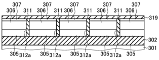
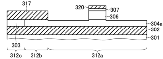
- the semiconductor laser according to the present invention comprises a first insulating layer formed on a substrate, a second insulating layer formed on the first insulating layer, first grooves arranged in a first direction at a plurality of locations on the second insulating layer, extending in a second direction perpendicular to the first direction and reaching the first insulating layer formed in the second insulating layer, second grooves formed in the second insulating layer in continuation with each of the first grooves in the second direction and reaching the first insulating layer with a width narrowing the further away from the first groove, third grooves formed in the second insulating layer in continuation with each of the second grooves in the second direction and reaching the first insulating layer, a silicon layer formed by filling each of the third grooves, a third insulating layer formed on the second insulating layer covering each of the first grooves, each of the second grooves, and each of the third grooves, and epitaxial growth from the side of the first groove side of each of the silicon layers.
- the resonator structure includes a first conductive type first semiconductor layer made of a compound semiconductor formed on the first insulating layer of each of the first grooves, an active layer made of a compound semiconductor formed on the first insulating layer of each of the first grooves by epitaxial growth from the side surface of the first semiconductor layer on the first groove side, a second conductive type second semiconductor layer made of a compound semiconductor formed on the first insulating layer of each of the first grooves by epitaxial growth from the side surface of the first groove side of each active layer, a first electrode connected to the first semiconductor layer through an opening formed in the third insulating layer, a second electrode connected to the second semiconductor layer through an opening formed in the third insulating layer, and a diffraction grating consisting of periodic divisions by the second insulating layer between adjacent first grooves, and performs light confinement in the active layer arranged in the first direction.
- the use of the second and third grooves makes it easier to increase the area of the p-type and n-type semiconductor layers on which the electrodes are formed, and a current injection type semiconductor laser using III-V compound semiconductor layers can be easily integrated with a Si waveguide.
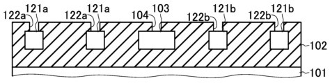
- FIG. 1 is a cross-sectional view showing the configuration of a semiconductor laser according to a first embodiment of the present invention.
- FIG. 2A is a cross-sectional view showing a state of a semiconductor laser in the middle of a process for explaining a method for manufacturing a semiconductor laser according to the first embodiment of the present invention.
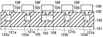
- FIG. 2B is a cross-sectional view showing a state of the semiconductor laser in the middle of a process for explaining a method of manufacturing the semiconductor laser according to the first embodiment of the present invention.
- FIG. 2C is a cross-sectional view showing a state of the semiconductor laser in the middle of a process for explaining a method of manufacturing the semiconductor laser according to the first embodiment of the present invention.
- FIG. 2A is a cross-sectional view showing a state of a semiconductor laser in the middle of a process for explaining a method for manufacturing a semiconductor laser according to the first embodiment of the present invention.
- FIG. 2B is a cross-sectional view showing a state of the semiconductor laser in the
- FIG. 2D is a cross-sectional view showing a state of the semiconductor laser in the middle of a process for explaining a method for manufacturing the semiconductor laser according to the first embodiment of the present invention.
- FIG. 2E is a cross-sectional view showing a state of the semiconductor laser in the middle of a process for explaining a method for manufacturing the semiconductor laser according to the first embodiment of the present invention.
- FIG. 2F is a cross-sectional view showing a state of the semiconductor laser in the middle of a process for explaining a method of manufacturing the semiconductor laser according to the first embodiment of the present invention.
- FIG. 3 is a characteristic diagram showing the optical confinement coefficient dependence of each layer (Si core 103, active layer 106, active layer structure 123) when the spacing (adjacent spacing L) between the active layer 106 and the active layer structure 123 adjacent to the active layer 106 is changed from 0.1 to 1 ⁇ m when the width of the Si core 103 is 440 nm.
- FIG. 4 is a characteristic diagram showing the optical confinement coefficient dependence for each layer (Si core 103, active layer 106, active layer structure 123) when the spacing (adjacent spacing L) between the active layer 106 and the active layer structure 123 adjacent to the active layer 106 is changed from 0.1 to 1 ⁇ m when the width of the Si core 103 is 700 nm.
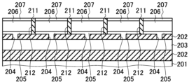
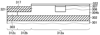
- FIG. 8 is a cross-sectional view showing a configuration of a semiconductor laser according to a second embodiment of the present invention.
- FIG. 9 is a plan view showing a configuration of a semiconductor laser according to the second embodiment of the present invention.
- FIG. 10A is a cross-sectional view showing a state of a semiconductor laser in the middle of a process for explaining a method for manufacturing a semiconductor laser according to the second embodiment of the present invention.
- FIG. 10B is a cross-sectional view showing a state of the semiconductor laser in the middle of a process for explaining a method for manufacturing a semiconductor laser according to the second embodiment of the present invention.
- FIG. 10A is a cross-sectional view showing a state of a semiconductor laser in the middle of a process for explaining a method for manufacturing a semiconductor laser according to the second embodiment of the present invention.
- FIG. 10B is a cross-sectional view showing a state of the semiconductor laser in the middle of a process for explaining a method for manufacturing a semiconductor laser according to
- FIG. 10C is a cross-sectional view showing a state of the semiconductor laser in the middle of a process for explaining a method for manufacturing a semiconductor laser according to the second embodiment of the present invention.
- FIG. 10D is a cross-sectional view showing a state of the semiconductor laser in the middle of a process for explaining a method for manufacturing a semiconductor laser according to the second embodiment of the present invention.
- FIG. 10E is a cross-sectional view showing a state of the semiconductor laser in the middle of a process for illustrating a method for manufacturing a semiconductor laser according to the second embodiment of the present invention.
- FIG. 10F is a cross-sectional view showing a state of the semiconductor laser in the middle of a process for explaining a method for manufacturing a semiconductor laser according to the second embodiment of the present invention.
- FIG. 17E is a cross-sectional view showing a state of a semiconductor laser in the middle of a process, for illustrating another method for manufacturing a semiconductor laser according to the third embodiment of the present invention.
- FIG. 17F is a cross-sectional view showing a state of a semiconductor laser in the middle of a process for illustrating another method for manufacturing a semiconductor laser according to the third embodiment of the present invention.
- FIG. 17G is a cross-sectional view showing a state of a semiconductor laser in the middle of a process, for illustrating a method for manufacturing another semiconductor laser according to the third embodiment of the present invention.
- FIG. 18 is an explanatory diagram illustrating aspect ratio trapping.
- This semiconductor laser includes a cladding layer 102 formed on a substrate 101, and a Si core 103 embedded in the cladding layer 102.
- the cladding layer 102 can be made of silicon oxide ( SiOx ) such as SiO2 .
- the Si core 103 extends from the front to the back of the paper in Fig. 1, and the Si core 103 and the cladding layer 102 form an optical waveguide.
- This semiconductor laser also has a second groove 122a that is formed in the cladding layer 102 above the first silicon layer 121a, extending along the Si core 103 and reaching the first silicon layer 121a.
- the bottom surface of the second groove 122a becomes the upper surface of the first silicon layer 121a.
- the second groove 122a is formed so that the groove depth is greater than the groove width.
- a third groove 122b is formed in the cladding layer 102 above the second silicon layer 121b, extending along the Si core 103 and reaching the second silicon layer 121b.
- the bottom surface of the third groove 122b becomes the upper surface of the first silicon layer 121a.
- the third groove 122b is formed so that the groove depth is greater than the groove width.
- the active layer 106 is formed on the lower semiconductor layer 105 in a state capable of optically coupling with the Si core 103.
- the active layer 106 is formed to extend along the Si core 103 together with the lower semiconductor layer 105.
- the active layer 106 can have a multiple quantum well structure in which well layers and barrier layers made of InGaAsP are alternately stacked.
- the active layer 106 can have a multiple quantum well structure in which well layers made of InGaAs and barrier layers made of InP are alternately stacked.
- the upper semiconductor layer 107 is formed on the active layer 106.
- the upper semiconductor layer 107 is formed to extend along the Si core 103 together with the active layer 106.
- the upper semiconductor layer 107 can be made of, for example, undoped InP (i-InP).
- the lower semiconductor layer 105 and the upper semiconductor layer 107 act as cladding layers to confine light in the active layer 106.
- the effective refractive index of the Si core 103 and the active layer 106 can be roughly matched, and the Si core 103 and the active layer 106 can be optically coupled with high efficiency.
- carriers can be injected into the active layer 106 more efficiently.
- a diffraction grating 112 is formed as a resonator structure that confines light to the active layer 106.
- the diffraction grating 112 is composed of, for example, a grating pattern formed on the top surface of the upper semiconductor layer 107.
- the semiconductor laser also includes a p-type semiconductor layer 108 formed on the cladding layer 102 and in contact with one surface of the active layer 106, and an n-type semiconductor layer 109 formed in contact with the other surface.
- the p-type semiconductor layer 108 is made of a compound semiconductor and is formed on the cladding layer 102 by epitaxial growth from the top surface of the first silicon layer 121a at the bottom surface of the second groove 122a, filling the second groove 122a.
- the n-type semiconductor layer 109 is made of a compound semiconductor and is formed on the cladding layer 102 by epitaxial growth from the top surface of the second silicon layer 121b at the bottom surface of the third groove 122b, filling the third groove 122b.
- the p-type semiconductor layer 108 and the n-type semiconductor layer 109 are formed to sandwich the lower semiconductor layer 105, the active layer 106, and the upper semiconductor layer 107 in a plan view. With this configuration, a current is injected into the active layer 106 in a direction parallel to the plane of the substrate 101.
- the p-type semiconductor layer 108 can be made of, for example, p-type InP doped with Zn at about 1 ⁇ 10 18 cm -3 .
- the n-type semiconductor layer 109 can be made of, for example, n-type InP doped with Si at about 1 ⁇ 10 18 cm -3 .
- the semiconductor laser also includes a p-type electrode 110 electrically connected to the p-type semiconductor layer 108, and an n-type electrode 111 electrically connected to the n-type semiconductor layer 109.
- the semiconductor laser also includes a first contact layer 114 formed on the p-type semiconductor layer 108, and a second contact layer 115 formed on the n-type semiconductor layer 109.
- the p-type electrode 110 is formed on the first contact layer 114 in ohmic contact, and the n-type electrode 111 is formed on the second contact layer 115 in ohmic contact.
- the first contact layer 114 can be made of p-type InGaAs.
- the second contact layer 115 can be made of n-type InGaAs.
- an insulating layer 113 is formed on and in contact with the upper semiconductor layer 107, the p-type semiconductor layer 108, and the n-type semiconductor layer 109 between the first contact layer 114 and the second contact layer 115.
- the lower semiconductor layer 105 is formed by epitaxially growing from the top surface of the Si core 103 at the bottom surface of the first groove 104 using the Si core 103 as a seed crystal, filling the first groove 104. This allows defects (dislocations) that occur at the interface between the lower semiconductor layer 105 and the Si core 103 to be terminated on the inner wall of the first groove 104, and the lower semiconductor layer 105 above the cladding layer 102 can be made into a good quality crystal.
- the width w of the first groove 104 is set to 100 (nm) and the height h of the first groove 104 is set to 150 (nm)
- a sufficient ART effect can be expected, and a good quality III-V compound semiconductor can be grown on the cladding layer 102.
- a good quality active layer 106 can be formed at a distance that allows optical coupling with the Si core 103.
- the above also applies to the p-type semiconductor layer 108 and the n-type semiconductor layer 109.
- the p-type semiconductor layer 108 is formed on the cladding layer 102 by epitaxial growth from the upper surface of the first silicon layer 121a at the bottom surface of the second groove 122a, filling the second groove 122a, so that it is easy to widen the width in the direction away from the active layer 106 in a planar view.
- the n-type semiconductor layer 108 is formed on the cladding layer 102 by epitaxial growth from the upper surface of the second silicon layer 121b at the bottom surface of the third groove 122b, filling the third groove 122b, so that it is easy to widen the width in the direction away from the active layer 106 in a planar view.
- pairs of first silicon layers 121a and second grooves 122a are provided at multiple locations in the direction away from the active layer 106 (first groove 104).
- layers of III-V compound semiconductor epitaxially grown from the first silicon layers 121a at multiple locations can be combined in a direction parallel to the plane of the substrate 101 to form a p-type semiconductor layer 108 with a larger area.
- the n-type semiconductor layer 109 For example, the width of the p-type semiconductor layer 108 and n-type semiconductor layer 109 in the direction away from the active layer 106 in a plan view can be set to 5 ⁇ m or more, which is necessary for electrode formation.
- a Si core 103, a first silicon layer 121a, and a second silicon layer 121b are formed on a substrate 101, and a clad layer 102 is formed to embed these.
- the Si core 103 and the clad layer 102 form an optical waveguide.
- the first groove 104, the second groove 122a, and the third groove 122b are formed in the cladding layer 102.
- the first groove 104 is formed in the cladding layer 102 above the Si core 103 so as to extend along the Si core 103 and reach the Si core 103.
- the second groove 122a is formed in the cladding layer 102 above the first silicon layer 121a so as to extend along the first silicon layer 121a and reach the first silicon layer 121a.
- the third groove 122b is formed in the cladding layer 102 above the second silicon layer 121a so as to extend along the second silicon layer 121b and reach the second silicon layer 121b.
- the first groove 104, the second groove 122a, and the third groove 122b can be formed by selectively etching away the cladding layer 102 using a dry etching process that uses a mask pattern formed by known lithography technology.
- Each groove is formed so that the groove depth is greater than the groove width.
- the first groove 104 is formed so that the groove width is 0.1 ⁇ m or less.
- a lower semiconductor layer 105 is formed on the cladding layer 102, filling the first groove 104 and extending along the Si core 103.
- the lower semiconductor layer 105 is formed by epitaxial growth from the upper surface of the Si core 103 at the bottom of the first groove 104.
- the lower semiconductor layer 105 is formed by epitaxially growing undoped InP using a well-known metalorganic vapor phase epitaxy method.
- the lower semiconductor layer 105' is epitaxially grown from the upper surfaces of the first silicon layer 121a and the second silicon layer 121b at the bottom of the second groove 122a and the third groove 122b.
- the lower semiconductor layer 105 is formed by epitaxial growth in a state where there are no defects above the cladding layer 102, by stopping the growth of defects that arise from the upper surface of the Si core 103 at the bottom of the first groove 104 at the side of the first groove 104 during the growth of a III-V compound semiconductor (e.g., InP) by aspect ratio trapping using the first groove 104.
- a III-V compound semiconductor e.g., InP
- the growth in the direction parallel to the plane of the substrate 101 is appropriately controlled, and the width of the lower semiconductor layer 105 in the width direction of the first groove 104 is formed to a set value.
- the lower semiconductor layer 105' is formed in the same manner as the lower semiconductor layer 105.
- an active layer 106 made of a III-V compound semiconductor is formed on the lower semiconductor layer 105, extending along the Si core 103 in a state capable of optically coupling with the Si core 103.
- the III-V compound semiconductor to be the active layer 106 is epitaxially grown from the upper surface of the lower semiconductor layer 105 to form the active layer 106.
- the sides of the lower semiconductor layer 105 are the upper surfaces of the cladding layer 102 made of a dielectric material such as silicon oxide, and the active layer 106 can be selectively grown only on the lower semiconductor layer 105 by appropriately setting the growth conditions of the III-V compound semiconductor.
- an active layer structure 106' having the same structure as the active layer 106 is formed on the lower semiconductor layer 105'.
- an upper semiconductor layer 107 made of a III-V compound semiconductor is formed on the active layer 106.
- the lower semiconductor layer 105 and the upper semiconductor layer 107 are formed by epitaxially growing undoped InP using the well-known metalorganic vapor phase epitaxy method.
- the sides of the lower semiconductor layer 105 are the upper surfaces of the cladding layer 102 made of a dielectric material such as silicon oxide, and the upper semiconductor layer 107 can be selectively grown only on the active layer 106 by appropriately setting the growth conditions for the III-V compound semiconductor.
- an upper semiconductor layer 107' having the same structure as the upper semiconductor layer 107 is formed on the active layer structure 106'.
- semiconductor layers 108a and 109a are formed to fill the sides of the active layer 106 and active layer structure 106'.
- a III-V compound semiconductor e.g., undoped InP
- the lower semiconductor layer 105' upper semiconductor layer 107'
- Both sides of the laminated structure of the lower semiconductor layer 105, active layer 106, and upper semiconductor layer 107 are filled with the grown semiconductor layers 108a and 109a.
- the top surfaces of the grown semiconductor layers 108a and 109a may not be flat, but in this case, they can be flattened using a technique such as chemical mechanical polisher (CMP).
- CMP chemical mechanical polisher
- the semiconductor layers 108a and 109a are formed by combining the III-V group compound semiconductors grown from the lower semiconductor layer 105' (upper semiconductor layer 107') at multiple locations. As a result, it is easy to form the semiconductor layers 108a and 109a with a wide width for forming electrodes on these layers. On the other hand, it is expected that defects such as twin planes and APBs will occur at the interface where the III-V group compound semiconductors are combined. In response to this, it is believed that it is possible to prevent deterioration of the optical characteristics by forming the active layer 106 at a location sufficiently far away from the combined interface so that such defects do not occur in the region of the active layer 106.
- a compound semiconductor layer e.g., undoped InGaAs
- a compound semiconductor layer e.g., undoped InGaAs
- a compound semiconductor layer e.g., undoped InGaAs
- the compound semiconductor layer on one side of the stacked structure of the lower semiconductor layer 105, active layer 106, and upper semiconductor layer 107 is doped with a p-type impurity to form the p-type semiconductor layer 108 and the first contact layer 114.
- the compound semiconductor layer on the other side of the stacked structure of the lower semiconductor layer 105, active layer 106, and upper semiconductor layer 107 is doped with an n-type impurity to form the n-type semiconductor layer 109 and the second contact layer 115.
- Figure 4 shows the dependence of the optical confinement coefficient for each layer (Si core 103, active layer 106, active layer structure 123) when the spacing (adjacent spacing L) between the active layer 106 and the active layer structure 123 adjacent to the active layer 106 is changed from 0.1 to 1 ⁇ m when the width of the Si core 103 is set to 700 nm.
- (a) shows the change in the optical confinement coefficient of the Si core 103.
- (b) shows the change in the optical confinement coefficient of the active layer 106.
- (c) shows the change in the total optical confinement coefficient of the Si core 103 and active layer 106.
- (d) shows the change in the optical confinement coefficient of the active layer structures 123 on the left and right of the active layer 106.
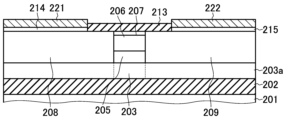
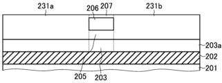
- Fig. 7 shows a cross section taken along line AA' in Fig. 9
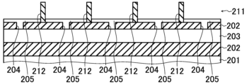
- Fig. 8 shows a cross section taken along line BB' in Fig. 9.
- This semiconductor laser first includes a cladding layer 202 formed on a substrate 201, and a Si core 203 embedded in the cladding layer 202.
- the cladding layer 202 can be made of silicon oxide (SiO x ) such as SiO 2.
- the Si core 203 extends from the front to the back of the paper in Fig. 7, and the Si core 203 and the cladding layer 202 form an optical waveguide.
- this semiconductor laser includes silicon layers 203a that are orthogonal to the Si core 203 in a direction parallel to the plane of the substrate 201 at each of a plurality of locations in the Si core 203 that are arranged in the waveguiding direction of the optical waveguide described above.
- the silicon layers 203a are formed in a rectangular core shape in cross section, and are positioned at the same height as the Si core 203 when viewed from the substrate 201.
- the semiconductor laser also includes a first groove 204 formed in the cladding layer 202.
- the first groove 204 is disposed on the silicon layer 203a and is formed to extend along the silicon layer 203a.
- the first groove 204 is also formed to reach the Si core 203 and silicon layer 203a in the thickness direction.
- the bottom surface of the first groove 204 becomes the upper surface of the Si core 203 and silicon layer 203a.
- the first groove 204 is formed so that the groove depth is greater than the groove width.
- the semiconductor laser also includes an insulating layer 211 formed on the cladding layer 202.
- a second groove 212 is formed in the insulating layer 211, reaching the cladding layer 202 (penetrating the insulating layer 211).
- the second groove 212 is disposed on each silicon layer 203a along the silicon layer 203a.
- this semiconductor laser includes a lower semiconductor layer 205, an active layer 206, and an upper semiconductor layer 207 made of III-V compound semiconductors in each of the second grooves 212 on the cladding layer 202.
- the laminated structures of the lower semiconductor layer 205, the active layer 206, and the upper semiconductor layer 207 are formed at multiple locations (intersections) of the Si core 203 that intersect with the silicon layer 203a.
- the laminated structures formed at the multiple intersections described above are arranged on the Si core 203 in the extension direction (waveguiding direction) of the Si core 203.
- the lower semiconductor layer 205 is formed on the cladding layer 202 by epitaxial growth from the top surface of the Si core 203 at the bottom surface of the first groove 204 in each of the second grooves 212, filling some of the first grooves 204.
- the lower semiconductor layer 205 is formed by epitaxial growth without defects above the cladding layer 202, by stopping the growth of defects generated from the top surface of the Si core 203 at the bottom surface of the first groove 204 at the side of the first groove 204 by aspect ratio trapping (ART) using the first groove 204.
- the lower semiconductor layer 205 can be composed of, for example, undoped InP.
- the lower semiconductor layer 205 can be formed directly above the Si core 203.
- the active layer 206 is formed on the lower semiconductor layer 205 in a state capable of optically coupling with the Si core 203.
- the active layer 206 can have a multiple quantum well structure in which well layers and barrier layers made of InGaAsP are alternately stacked. It can also have a multiple quantum well structure in which well layers made of InGaAs and barrier layers made of InP are alternately stacked.
- the upper semiconductor layer 207 is formed on the active layer 206.
- the upper semiconductor layer 207 can be composed of, for example, undoped InP (i-InP).
- the lower semiconductor layer 205 and the upper semiconductor layer 207 can be clad to confine light to the active layer 206.
- the effective refractive index of the Si core 203 and the active layer 206 can be roughly matched, and the Si core 203 and the active layer 206 can be optically coupled with high efficiency.
- carriers can be injected into the active layer 206 more efficiently.
- This semiconductor laser also has a resonator structure that is composed of a diffraction grating (grating pattern) consisting of periodically arranged partitions made of the insulating layer 211 between adjacent second grooves 212, and that confines light to the active layer 206 arranged in the waveguide direction.
- This resonator structure is a structure in which both the refractive index and gain change periodically with respect to the resonance direction (waveguiding direction), and is a complex coupling type laser structure.
- the period of the insulating layer 211 between adjacent second grooves 212 needs to be appropriately designed for the target oscillation wavelength.
- the semiconductor laser also includes a p-type semiconductor layer 208 formed on the cladding layer 202 and in contact with one surface of the active layer 206, and an n-type semiconductor layer 209 formed in contact with the other surface.
- the p-type semiconductor layer 208 is made of a compound semiconductor, and in each of the second grooves 212, it grows epitaxially from the top surface of the silicon layer 203a at the bottom of the first groove 204, filling a portion of the first groove 204, and is formed on the cladding layer 202 and in contact with the side of the active layer 206.
- the n-type semiconductor layer 209 is made of a compound semiconductor, and in each of the second grooves 212, it grows epitaxially from the top surface of the silicon layer 203a at the bottom of the first groove 204, filling a portion of the first groove 204, and is formed on the cladding layer 202 and in contact with the side of the active layer 206.
- the p-type semiconductor layer 208 and the n-type semiconductor layer 209 are formed to sandwich the lower semiconductor layer 205, the active layer 206, and the upper semiconductor layer 207 in a plan view. With this configuration, a current is injected into the active layer 206 in a direction parallel to the plane of the substrate 201.
- the p-type semiconductor layer 208 can be made of, for example, p-type InP doped with Zn at about 1 ⁇ 10 18 cm -3 .
- the n-type semiconductor layer 209 can be made of, for example, n-type InP doped with Si at about 1 ⁇ 10 18 cm -3 .
- the semiconductor laser also includes a p-type electrode 221 electrically connected to the p-type semiconductor layer 208, and an n-type electrode 222 electrically connected to the n-type semiconductor layer 209.
- the semiconductor laser also includes a first contact layer 214 formed on the p-type semiconductor layer 208, and a second contact layer 215 formed on the n-type semiconductor layer 209.
- the p-type electrode 221 is formed on the first contact layer 214 in ohmic contact, and the n-type electrode 222 is formed on the second contact layer 215 in ohmic contact.
- the first contact layer 214 may be made of p-type InP doped with Zn at about 1 ⁇ 10 19 cm ⁇ 3 .
- the second contact layer 215 may be made of n-type InP doped with Si at about 1 ⁇ 10 19 cm ⁇ 3 .
- an insulating layer 213 is formed on and in contact with the upper semiconductor layer 207, the p-type semiconductor layer 208, and the n-type semiconductor layer 209 between the first contact layer 214 and the second contact layer 215.
- the lower semiconductor layer 205 is formed by epitaxially growing from the top surface of the Si core 203 at the bottom surface of the first groove 204 using the Si core 203 as a seed crystal, filling the first groove 204 above the Si core 203. This allows defects (dislocations) that occur at the interface between the lower semiconductor layer 205 and the Si core 203 to be terminated on the inner wall of the first groove 204, and the lower semiconductor layer 205 above the cladding layer 202 can be made into a good quality crystal.
- the width w of the first groove 204 is set to 100 (nm) and the height h of the first groove 204 is set to 150 (nm)
- a sufficient ART effect can be expected, and a good quality III-V compound semiconductor can be grown on the cladding layer 202.
- a good quality active layer 206 can be formed at a distance that allows optical coupling with the Si core 203.
- the above also applies to the p-type semiconductor layer 208 and the n-type semiconductor layer 209.
- the p-type semiconductor layer 208 is epitaxially grown from the upper surface of the silicon layer 203a at the bottom of the first groove 204, filling the first groove 204 in this region and formed on the clad layer 202, so that it is easy to widen the width in the direction away from the active layer 206 in a planar view.
- the n-type semiconductor layer 209 is epitaxially grown from the upper surface of the silicon layer 203a at the bottom of the first groove 204, filling the first groove 204 in this region and formed on the clad layer 202, so that it is easy to widen the width in the direction away from the active layer 206 in a planar view.
- twin planes and APBs are not generated in the crystal growth of the III-V compound semiconductors that form the p-type semiconductor layer 208 and the n-type semiconductor layer 209, so that it is expected that there will be no decrease in internal quantum efficiency due to non-radiative recombination of carriers.
- a Si core 203 and a silicon layer 203a are formed on a substrate 201, and a clad layer 202 is formed in which they are embedded.
- the Si core 203 and the clad layer 202 form an optical waveguide.
- a first groove 204 is also formed in the clad layer 202.
- an insulating layer 211 is formed on the clad layer 202, and second grooves 212 are formed in multiple locations in the formed insulating layer 211.
- the first groove 204 can be formed by selectively etching away the cladding layer 202 using a dry etching process that uses a mask pattern formed by known lithography technology.
- the second groove 212 can be formed by selectively etching away the insulating layer 211 using a dry etching process that uses a mask pattern formed by known lithography technology.
- a lower semiconductor layer 205 that fills the first groove 204 and extends along the Si core 203 is formed on the cladding layer 202.
- the lower semiconductor layer 205 is formed by epitaxial growth from the upper surface of the Si core 203 and the silicon layer 203a at the bottom surface of the first groove 204.
- the lower semiconductor layer 205 is formed by epitaxially growing undoped InP using the well-known metalorganic vapor phase epitaxy method.
- the lower semiconductor layer 205 is formed by epitaxial growth without defects above the cladding layer 202, by stopping the growth of defects that occur from the Si core 203 at the bottom of the first groove 204 and the top surface of the silicon layer 203a at the side of the first groove 204 during the growth of the III-V compound semiconductor (e.g., InP) through aspect ratio trapping using the first groove 204.
- the III-V compound semiconductor e.g., InP
- an active layer 206 made of a III-V compound semiconductor is formed on the lower semiconductor layer 205, extending along the Si core 203 in a state capable of optically coupling with the Si core 203.
- the III-V compound semiconductor that will become the active layer 206 is epitaxially grown from the upper surface of the lower semiconductor layer 205 to form the active layer 206.
- an upper semiconductor layer 207 made of a III-V compound semiconductor is formed on the active layer 206.
- the upper semiconductor layer 207 is formed on the active layer 206 by epitaxially growing undoped InP using the well-known metalorganic vapor phase epitaxy method.
Landscapes
- Physics & Mathematics (AREA)
- Condensed Matter Physics & Semiconductors (AREA)
- General Physics & Mathematics (AREA)
- Electromagnetism (AREA)
- Optics & Photonics (AREA)
- Semiconductor Lasers (AREA)
Priority Applications (2)
| Application Number | Priority Date | Filing Date | Title |
|---|---|---|---|
| JP2025535528A JPWO2025022644A1 (https=) | 2023-07-27 | 2023-07-27 | |
| PCT/JP2023/027571 WO2025022644A1 (ja) | 2023-07-27 | 2023-07-27 | 半導体レーザ |
Applications Claiming Priority (1)
| Application Number | Priority Date | Filing Date | Title |
|---|---|---|---|
| PCT/JP2023/027571 WO2025022644A1 (ja) | 2023-07-27 | 2023-07-27 | 半導体レーザ |
Publications (1)
| Publication Number | Publication Date |
|---|---|
| WO2025022644A1 true WO2025022644A1 (ja) | 2025-01-30 |
Family
ID=94374582
Family Applications (1)
| Application Number | Title | Priority Date | Filing Date |
|---|---|---|---|
| PCT/JP2023/027571 Pending WO2025022644A1 (ja) | 2023-07-27 | 2023-07-27 | 半導体レーザ |
Country Status (2)
| Country | Link |
|---|---|
| JP (1) | JPWO2025022644A1 (https=) |
| WO (1) | WO2025022644A1 (https=) |
Citations (7)
| Publication number | Priority date | Publication date | Assignee | Title |
|---|---|---|---|---|
| JPS62213117A (ja) * | 1986-03-13 | 1987-09-19 | Oki Electric Ind Co Ltd | 半導体素子の製造方法 |
| JPH05206565A (ja) * | 1991-06-12 | 1993-08-13 | Oki Electric Ind Co Ltd | 半導体レーザ素子 |
| JP2004055797A (ja) * | 2002-07-19 | 2004-02-19 | Fujitsu Ltd | 分布帰還型半導体レーザ |
| JP2010171262A (ja) * | 2009-01-23 | 2010-08-05 | Sumitomo Electric Ind Ltd | 半導体レーザを作製する方法および半導体レーザ |
| JP2016103594A (ja) * | 2014-11-28 | 2016-06-02 | 三菱電機株式会社 | 半導体光素子および面発光半導体光素子 |
| WO2021005700A1 (ja) * | 2019-07-09 | 2021-01-14 | 日本電信電話株式会社 | 半導体光素子 |
| US20210273409A1 (en) * | 2020-02-27 | 2021-09-02 | Qualcomm Incorporated | Distributed feedback (dfb) laser on silicon and integrated device comprising a dfb laser on silicon |
-
2023
- 2023-07-27 JP JP2025535528A patent/JPWO2025022644A1/ja active Pending
- 2023-07-27 WO PCT/JP2023/027571 patent/WO2025022644A1/ja active Pending
Patent Citations (7)
| Publication number | Priority date | Publication date | Assignee | Title |
|---|---|---|---|---|
| JPS62213117A (ja) * | 1986-03-13 | 1987-09-19 | Oki Electric Ind Co Ltd | 半導体素子の製造方法 |
| JPH05206565A (ja) * | 1991-06-12 | 1993-08-13 | Oki Electric Ind Co Ltd | 半導体レーザ素子 |
| JP2004055797A (ja) * | 2002-07-19 | 2004-02-19 | Fujitsu Ltd | 分布帰還型半導体レーザ |
| JP2010171262A (ja) * | 2009-01-23 | 2010-08-05 | Sumitomo Electric Ind Ltd | 半導体レーザを作製する方法および半導体レーザ |
| JP2016103594A (ja) * | 2014-11-28 | 2016-06-02 | 三菱電機株式会社 | 半導体光素子および面発光半導体光素子 |
| WO2021005700A1 (ja) * | 2019-07-09 | 2021-01-14 | 日本電信電話株式会社 | 半導体光素子 |
| US20210273409A1 (en) * | 2020-02-27 | 2021-09-02 | Qualcomm Incorporated | Distributed feedback (dfb) laser on silicon and integrated device comprising a dfb laser on silicon |
Non-Patent Citations (2)
| Title |
|---|
| LI, Z. ET AL.: "Monolithic integration of InGaAs/InP multiple quantum wells on SOI substrates for photonic devices", JOURNAL OF APPLIED PHYSICS, vol. 123, February 2018 (2018-02-01), pages 053102 - 1, XP012226151, DOI: 10.1063/1.5009639 * |
| TRAN, M. A. ET AL.: "Tutorial on narrow linewidth tunable semiconductor lasers using Si/ III-V heterogeneous integration", APL PHOTONICS, vol. 4, November 2019 (2019-11-01), pages 111101 - 1, XP012241940, DOI: 10.1063/1.5124254 * |
Also Published As
| Publication number | Publication date |
|---|---|
| JPWO2025022644A1 (https=) | 2025-01-30 |
Similar Documents
| Publication | Publication Date | Title |
|---|---|---|
| US8290014B2 (en) | Active photonic device | |
| US7941024B2 (en) | Buried heterostructure device having integrated waveguide grating fabricated by single step MOCVD | |
| EP0663710B1 (en) | Optical semiconductor device and method for producing the same | |
| JPH0738204A (ja) | 半導体光デバイス及びその製造方法 | |
| JP2746326B2 (ja) | 半導体光素子 | |
| JP6839035B2 (ja) | 半導体装置の製造方法 | |
| JP2007243019A (ja) | 光半導体素子 | |
| EP0486128B1 (en) | A semiconductor optical device and a fabricating method therefor | |
| CN118825769B (zh) | 侧向非晶硅光子晶体激光器、激光器阵列及制备方法 | |
| GB2287124A (en) | Semiconductor laser and method of fabrication | |
| JPH05251817A (ja) | 可変波長半導体レーザ装置 | |
| JP4909159B2 (ja) | 半導体導波路素子およびその作製方法ならびに半導体レーザ | |
| US20230318263A1 (en) | Optoelectronic device comprising a iii-v semiconductor membrane laser source forming a lateral p-i-n junction | |
| US20230021415A1 (en) | Manufacturing Method for Semiconductor Device | |
| WO2025022644A1 (ja) | 半導体レーザ | |
| JP4097950B2 (ja) | 分布帰還型レーザ装置、半導体光装置および分布帰還型レーザ装置の製造方法 | |
| JPH05110187A (ja) | アレイ型半導体レーザ及びその製造方法 | |
| JPH0716079B2 (ja) | 半導体レ−ザ装置 | |
| WO2025022643A1 (ja) | 半導体レーザおよびその製造方法 | |
| JP4447222B2 (ja) | 分布帰還型半導体レーザ | |
| US20230139692A1 (en) | Semiconductor Optical Device | |
| JP4192324B2 (ja) | 半導体レーザ素子およびその製造方法 | |
| JPS6046087A (ja) | 分布ブラッグ反射型半導体レ−ザ | |
| JP6622152B2 (ja) | 光素子 | |
| JP2687884B2 (ja) | 波長可変半導体レーザ及びその製造方法 |
Legal Events
| Date | Code | Title | Description |
|---|---|---|---|
| 121 | Ep: the epo has been informed by wipo that ep was designated in this application |
Ref document number: 23946724 Country of ref document: EP Kind code of ref document: A1 |
|
| ENP | Entry into the national phase |
Ref document number: 2025535528 Country of ref document: JP Kind code of ref document: A |
|
| WWE | Wipo information: entry into national phase |
Ref document number: 2025535528 Country of ref document: JP |
|
| NENP | Non-entry into the national phase |
Ref country code: DE |