WO2025018005A1 - 積層セラミック電子部品 - Google Patents
積層セラミック電子部品 Download PDFInfo
- Publication number
- WO2025018005A1 WO2025018005A1 PCT/JP2024/017064 JP2024017064W WO2025018005A1 WO 2025018005 A1 WO2025018005 A1 WO 2025018005A1 JP 2024017064 W JP2024017064 W JP 2024017064W WO 2025018005 A1 WO2025018005 A1 WO 2025018005A1
- Authority
- WO
- WIPO (PCT)
- Prior art keywords
- layer
- layer portion
- outer layer
- internal electrode
- additive
- Prior art date
- Legal status (The legal status is an assumption and is not a legal conclusion. Google has not performed a legal analysis and makes no representation as to the accuracy of the status listed.)
- Pending
Links
Images


Classifications
-
- H—ELECTRICITY
- H01—ELECTRIC ELEMENTS
- H01G—CAPACITORS; CAPACITORS, RECTIFIERS, DETECTORS, SWITCHING DEVICES, LIGHT-SENSITIVE OR TEMPERATURE-SENSITIVE DEVICES OF THE ELECTROLYTIC TYPE
- H01G4/00—Fixed capacitors; Processes of their manufacture
- H01G4/30—Stacked capacitors
-
- H—ELECTRICITY
- H01—ELECTRIC ELEMENTS
- H01G—CAPACITORS; CAPACITORS, RECTIFIERS, DETECTORS, SWITCHING DEVICES, LIGHT-SENSITIVE OR TEMPERATURE-SENSITIVE DEVICES OF THE ELECTROLYTIC TYPE
- H01G4/00—Fixed capacitors; Processes of their manufacture
- H01G4/002—Details
- H01G4/005—Electrodes
- H01G4/008—Selection of materials
- H01G4/0085—Fried electrodes
-
- H—ELECTRICITY
- H01—ELECTRIC ELEMENTS
- H01G—CAPACITORS; CAPACITORS, RECTIFIERS, DETECTORS, SWITCHING DEVICES, LIGHT-SENSITIVE OR TEMPERATURE-SENSITIVE DEVICES OF THE ELECTROLYTIC TYPE
- H01G4/00—Fixed capacitors; Processes of their manufacture
- H01G4/002—Details
- H01G4/005—Electrodes
- H01G4/012—Form of non-self-supporting electrodes
-
- H—ELECTRICITY
- H01—ELECTRIC ELEMENTS
- H01G—CAPACITORS; CAPACITORS, RECTIFIERS, DETECTORS, SWITCHING DEVICES, LIGHT-SENSITIVE OR TEMPERATURE-SENSITIVE DEVICES OF THE ELECTROLYTIC TYPE
- H01G4/00—Fixed capacitors; Processes of their manufacture
- H01G4/002—Details
- H01G4/018—Dielectrics
- H01G4/06—Solid dielectrics
- H01G4/08—Inorganic dielectrics
- H01G4/12—Ceramic dielectrics
- H01G4/1209—Ceramic dielectrics characterised by the ceramic dielectric material
- H01G4/1218—Ceramic dielectrics characterised by the ceramic dielectric material based on titanium oxides or titanates
- H01G4/1227—Ceramic dielectrics characterised by the ceramic dielectric material based on titanium oxides or titanates based on alkaline earth titanates
-
- H—ELECTRICITY
- H01—ELECTRIC ELEMENTS
- H01G—CAPACITORS; CAPACITORS, RECTIFIERS, DETECTORS, SWITCHING DEVICES, LIGHT-SENSITIVE OR TEMPERATURE-SENSITIVE DEVICES OF THE ELECTROLYTIC TYPE
- H01G4/00—Fixed capacitors; Processes of their manufacture
- H01G4/002—Details
- H01G4/228—Terminals
- H01G4/232—Terminals electrically connecting two or more layers of a stacked or rolled capacitor
Definitions
- the present invention relates to multilayer ceramic electronic components.
- Multilayer ceramic electronic components such as multilayer ceramic capacitors are manufactured by stacking multiple dielectric sheets. Internal electrode layers are formed on the dielectric sheets to form capacitors, resistors, inductors, varistors, filters, etc., depending on the multilayer ceramic electronic component. Progress is being made in making these multilayer ceramic electronic components thinner and more multilayered in order to achieve smaller size and higher performance. For example, see Patent Document 1.
- Patent Document 1 even if the dielectric sheets are made thinner and more multi-layered, the internal electrode layers may not be made thinner.
- the thinned dielectric sheets and internal electrode layers are alternately stacked, and the internal electrode layers are alternately exposed at both longitudinal end faces of the dielectric sheets and drawn out alternately to a pair of external electrodes with opposite polarity, a laminate is formed with a step due to the thickness of the dielectric sheets and the thickness of the internal electrode layers.
- the ceramic of the dielectric sheet flows to fill the steps due to the thickness, which reduces the thickness of the dielectric sheet near the steps, and the thinned sheet can become even thinner.
- the edge effect causes the electric field strength to be greater at the end of the internal electrode layer near the step than in other areas of the internal electrode layer.
- electric field concentration occurs more at the end of the internal electrode layer near the step, which may cause insulation breakdown.
- the present invention aims to provide a multilayer ceramic electronic component, such as a multilayer ceramic capacitor, that has high reliability.
- a multilayer ceramic electronic component that can suppress the occurrence of dielectric breakdown at the ends of the internal electrode layers that are exposed to a strong electric field.
- the multilayer ceramic electronic component of the present invention has a plurality of laminated dielectric layers, a plurality of first internal electrode layers and a plurality of second internal electrode layers laminated on the dielectric layers, a laminate having a first main surface and a second main surface facing each other in a lamination direction, a first end surface and a second end surface facing each other in a length direction perpendicular to the lamination direction, a first side surface and a second side surface facing each other in a width direction perpendicular to the lamination direction and the length direction, a first external electrode arranged on the first end surface, and a second external electrode arranged on the second end surface, the plurality of first internal electrode layers being electrically connected to the first external electrode, the plurality of second internal electrode layers being electrically connected to the second external electrode, and the laminate having a first internal electrode layer and a second internal electrode layer.
- a multilayer ceramic electronic component having an inner layer portion facing the plurality of second internal electrode layers, the concentration of the additive contained on the first side surface side of the inner layer portion is higher than that of the central portion in the width direction of the inner layer portion, the concentration of the additive contained on the second side surface side of the inner layer portion is higher than that of the central portion in the width direction of the inner layer portion, the concentration of the additive at the end of the second internal electrode layer on the first end surface side of the inner layer portion is higher than that of the central portion of the inner layer portion, the concentration of the additive at the end of the first internal electrode layer on the second end surface side of the inner layer portion is higher than that of the central portion of the inner layer portion, and the additive contains at least one of V, Mn, and Mg.
- the present invention makes it possible to provide highly reliable multilayer ceramic electronic components, such as multilayer ceramic capacitors.
- FIG. 1 is a perspective view of a multilayer ceramic electronic component according to an embodiment of the present invention.
- 2 is a cross-sectional view taken along line II in FIG. 1.
- 2 is a cross-sectional view taken along line II-II of FIG. 1. 1.
- a cross-sectional view taken along line III-III in FIG. 2 is a cross-sectional view corresponding to the line II-II cross-sectional view of FIG. 1 according to the second embodiment.
- FIG. 2 is a diagram showing an outline of a laminate core portion.
- FIG. 2 is a perspective view showing a polished inner layer portion.
- FIG. 2 is a perspective view showing a polished inner layer portion.
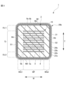
- FIG 1 is a perspective view of a multilayer ceramic capacitor 1 according to a first embodiment of the present invention.
- the laminate 2 includes a plurality of laminated dielectric layers and a plurality of internal electrode layers.
- the laminate 2 has an approximately rectangular parallelepiped shape.
- the direction in which the dielectric layers and the internal electrode layers are laminated is defined as a lamination direction T.
- the direction perpendicular to the lamination direction T is defined as a width direction W.
- the direction perpendicular to the lamination direction T and the width direction W is defined as a length direction L.
- the two surfaces that face each other in the stacking direction T are respectively the first main surface M1 and the second main surface M2.
- the two surfaces that face each other in the width direction W are respectively the first side surface S1 and the second side surface.
- they are respectively the first end surface E1 and the second end surface E2 that face each other in the length direction L.
- the mounting surface of the multilayer ceramic capacitor 1 is the second main surface M2.
- the mounting surface is the surface that faces the wiring board when the multilayer ceramic capacitor 1 is mounted on a wiring board or the like.
- the cross section taken along line I-I in FIG. 1 is defined as the LT cross section.
- the cross section taken along line II-II in FIG. 1 is defined as the WT cross section.
- the cross section taken along line III-III in FIG. 1 is defined as the LW cross section.
- the corners and ridges of the laminate 2 are rounded.
- a corner is a portion where three faces of the laminate 2 intersect.
- a ridge is a portion where two faces of the laminate 2 intersect.
- unevenness may be formed on some or all of the main surface, side surface, and end surface.
- the total number of dielectric layers laminated in the laminate 2 is preferably 15 or more and 2000 or less.
- the dielectric layers are mainly formed of a ceramic material.
- a ceramic material for example, a dielectric ceramic composed of a main component such as BaTiO3 , CaTiO3 , SrTiO3 , or CaZrO3 can be used.
- a dielectric ceramic in which a subcomponent such as a Mn compound, an Fe compound, a Cr compound, a Co compound, or a Ni compound is added to these main components may be used as the ceramic material.
- the multilayer ceramic electronic component will be described using a multilayer ceramic capacitor 1, which is one type of multilayer ceramic electronic component, as an example.
- the laminated ceramic electronic component functions as a ceramic piezoelectric element.
- piezoelectric ceramic materials include PZT (lead zirconate titanate) ceramic materials.
- the multilayer ceramic electronic component functions as a thermistor element.
- semiconductor ceramic materials include spinel ceramic materials.
- the multilayer ceramic electronic component functions as an inductor element.
- the internal electrode layer becomes a coil-shaped conductor.
- a specific example of a magnetic ceramic material is a ferrite ceramic material.
- each dielectric layer is preferably 0.5 ⁇ m or more and 10 ⁇ m or less.
- Fig. 2 is a cross-sectional view taken along line II in Fig. 1.
- the laminate 2 can be divided into a first main surface side outer layer portion OL1, an inner layer range IL, and a second main surface side outer layer portion OL2 in the stacking direction T.
- the first main surface side outer layer portion OL1, the inner layer range IL, and the second main surface side outer layer portion OL2 are arranged in this order from the first main surface M1 to the second main surface M2 in the stacking direction T.
- the first main surface side outer layer portion OL1 is the portion between the first main surface M1 and a line drawn from the first end face E1 to the second end face E2 along the surface of the internal electrode layer closest to the first main surface M1.
- the second main surface side outer layer portion OL2 is the portion between the second main surface M2 and a line drawn from the first end face E1 to the second end face E2 along the surface of the internal electrode layer closest to the second main surface M2.
- the internal layer range IL is the range sandwiched between the first main surface side outer layer portion OL1 and the second main surface side outer layer portion OL2.
- the internal layer range IL is the range between a line drawn from the first end face E1 to the second end face E2 along the surface of the internal electrode layer closest to the first main surface M1, and a line drawn from the line drawn from the second end face E2 to the first end face E1 along the surface of the internal electrode layer closest to the second main surface M2.
- the first main surface side outer layer portion OL1 is located on the first main surface M1 side of the laminate 2.
- the first main surface side outer layer portion OL1 can be an assembly of multiple dielectric layers located between a line drawn from the first end face E1 to the second end face E2 along the first main surface M1 and the outermost surface of the internal electrode layer closest to the first main surface M1.
- the second main surface side outer layer portion OL2 is located on the second main surface M2 side of the laminate 2.
- the second main surface side outer layer portion OL2 can be a collection of multiple dielectric layers located between a line drawn from the first end face E1 to the second end face E2 along the second main surface M2 and the outermost surface of the internal electrode layer closest to the second main surface M2 and the line and the second main surface M2.
- the first main surface side outer layer portion OL1 is located on the first main surface M1 side, and is formed from a plurality of dielectric layers located between the first main surface M1 and the outermost surface of the inner layer range IL on the first main surface M1 side and an extension of that outermost surface.
- the second main surface side outer layer portion OL2 is located on the second main surface M2 side, and is formed from a plurality of dielectric layers located between the second main surface M2 and the outermost surface of the inner layer range IL on the second main surface M2 side and an extension of that outermost surface.
- the inner layer range IL is the range sandwiched between the first main surface side outer layer portion OL1 and the second main surface side outer layer portion OL2.
- the dielectric layers disposed in the first main surface side outer layer portion OL1 and the second main surface side outer layer portion OL2 are referred to as outer dielectric layer 3.
- the dielectric layers disposed in the inner layer range IL are referred to as inner dielectric layer 4.
- the dimensions of the laminate 2 are not particularly limited.
- the dimension in the length direction L of the laminate 2 is taken as the L dimension.
- the L dimension is preferably 0.2 mm or more and 10 mm or less.
- the dimension in the width direction W of the laminate 2 is taken as the W dimension.
- the W dimension is preferably 0.1 mm or more and 5 mm or less.
- the dimension in the stacking direction T of the laminate 2 is taken as the T dimension.
- the T dimension is preferably 0.1 mm or more and 5 mm or less.
- the laminate 2 can be divided into a first end surface side outer layer portion LG1, an L-facing portion LF, and a second end surface side outer layer portion LG2 in the longitudinal direction L.
- the first end surface side outer layer portion LG1, the L-facing portion LF, and the second end surface side outer layer portion LG2 are arranged in this order in the longitudinal direction L from the first end surface E1 to the second end surface E2.
- the first end surface side outer layer portion LG1 is a portion where only the first internal electrode layers 6a face each other in the stacking direction T, and is a portion between the first main surface side outer layer portion OL1 and the second main surface side outer layer portion OL2.
- the second end surface side outer layer portion LG2 is a portion where only the second internal electrode layers 6b face each other in the stacking direction T, and is a portion between the first main surface side outer layer portion OL1 and the second main surface side outer layer portion OL2.
- the L opposing portion LF is a region sandwiched between the first end surface side outer layer portion LG1 and the second end surface side outer layer portion LG2.
- the L opposing portion LF is a portion where the first internal electrode layer 6a and the second internal electrode layer 6b face each other in the stacking direction T.
- the L opposing portion LF is a portion corresponding to the opposing electrode portion of the internal electrode layer.
- the first end surface side outer layer portion LG1 and the second end surface side outer layer portion LG2 are portions that correspond to the lead-out electrode portions of the internal electrode layer. The opposing electrode portion and the lead-out electrode portion will be explained later.
- the first end surface side outer layer portion LG1 and the second end surface side outer layer portion LG2 are also called L gaps.
- the first end face side outer layer portion LG1 is located on the first end face E1 side, and is located between the outermost surface on the first end face E1 side and the outermost surface of the end of the second internal electrode layer 6b that is not connected to the first external electrode 20a.
- the second end face side outer layer portion LG2 is located on the second end face E2 side, and is located between the outermost surface on the second end face E2 side and the outermost surface of the end of the first internal electrode layer 6a that is not connected to the second external electrode 20b.
- FIG. 3 is a cross-sectional view of line II-II in FIG. 1.
- the laminate 2 can be divided into a first main surface side outer layer portion OL1, an inner layer range IL, and a second main surface side outer layer portion OL2 in the stacking direction T.
- the first main surface side outer layer portion OL1 is a portion between a line drawn from the first side surface S1 to the second side surface S2 along the outermost surface of the internal electrode layer closest to the first main surface M1 and the first main surface M1.
- the second main surface side outer layer portion OL2 is a portion between a line drawn from the first side surface S1 to the second side surface S2 along the outermost surface of the internal electrode layer closest to the second main surface M2 and the second main surface M2.
- the inner layer range IL is a range sandwiched between the first main surface side outer layer portion OL1 and the second main surface side outer layer portion OL2. That is, the inner layer range IL is the range between a line drawn from the first side surface S1 to the second side surface S2 along the outermost surface of the internal electrode layer closest to the first main surface M1, and a line drawn from the line drawn from the second side surface S2 to the first side surface S1 along the outermost surface of the internal electrode layer closest to the second main surface M2.
- the dielectric layers arranged in the first main surface side outer layer portion OL1 and the second main surface side outer layer portion OL2 are referred to as outer layer dielectric layers 3.
- the dielectric layers arranged in the inner layer range IL2 are referred to as inner layer dielectric layers 4.
- the laminate 2 can be divided into a first side surface outer layer portion WG1, a W-facing portion WF, and a second side surface outer layer portion WG2 in the width direction W.
- the first side surface outer layer portion WG1, the W-facing portion WF, and the second side surface outer layer portion WG2 are arranged in this order in the width direction W from the first side surface S1 to the second side surface S2.
- the W facing portion WF is the portion where the internal electrode layers face each other in the stacking direction T.
- the first side surface side outer layer portion WG1 is the portion between the W facing portion WF, the first side surface S1, the first main surface side outer layer portion OL1, and the second main surface side outer layer portion OL2.
- the second side surface side outer layer portion WG2 is the portion between the W facing portion WF, the second side surface S2, the first main surface side outer layer portion OL1, and the second main surface side outer layer portion OL2.
- the first side surface side outer layer portion WG1 and the second side surface side outer layer portion WG2 are also called the W gap.
- the first side surface side outer layer portion WG1 and the second side surface side outer layer portion WG2 are portions where no internal electrode layer is present in the stacking direction T.
- the first side surface side outer layer portion WG1 is located on the first side surface S1 side, is a portion where no internal electrode is present in the stacking direction T, and is a portion sandwiched between the first main surface side outer layer portion OL1 and the second main surface side outer layer portion OL2.
- the first side surface side outer layer portion WG1 is located on the first side surface S1 side, and can be formed from a plurality of dielectric layers located between the first side surface S1, the first main surface side outer layer portion OL1, the second main surface side outer layer portion OL2, and the outermost surface of the inner layer portion on the first side surface S1 side.
- the second side surface side outer layer portion WG2 is located on the second side surface S2 side, is a portion in which no internal electrode is present in the stacking direction T, and is a portion sandwiched between the first main surface side outer layer portion OL1 and the second main surface side outer layer portion OL2.
- the second side surface side outer layer portion WG2 is located on the second side surface S2 side, and can be formed from a plurality of dielectric layers located between the second side surface S2, the first main surface side outer layer portion OL1, the second main surface side outer layer portion OL2, and the outermost surface of the inner layer portion on the second side surface S2 side.
- the internal electrode layers include a plurality of first internal electrode layers 6a and a plurality of second internal electrode layers 6b.
- the first internal electrode layers 6a are internal electrode layers exposed at the first end face E1.
- the second internal electrode layers 6b are internal electrode layers exposed at the second end face E2.
- the first internal electrode layer 6a has a first opposing electrode portion 7a that faces the second internal electrode layer 6b, and a first extraction electrode portion 8a that is drawn from the first opposing electrode portion 7a to the first end face E1 of the laminate 2.
- the end of the first extraction electrode portion 8a on the first end face E1 side is drawn to the surface of the first end face E1 of the laminate 2.
- the end of the first extraction electrode portion 8a that is drawn to the first end face E1 forms an exposed portion at the first end face E1.
- the second internal electrode layer 6b has a second opposing electrode portion 7b that faces the first internal electrode layer 6a, and a second extraction electrode portion 8b that is drawn from the second opposing electrode portion 7b to the second end face E2 of the laminate 2.
- the end of the second extraction electrode portion 8b on the second end face E2 side is drawn to the surface of the second end face E2 of the laminate 2.
- the end of the second extraction electrode portion 8b that is drawn to the second end face E2 forms an exposed portion at the second end face E2.
- the shape of the first opposing electrode portion 7a and the second opposing electrode portion 7b is preferably rectangular, but the shape of the first opposing electrode portion 7a and the second opposing electrode portion 7b is not particularly limited. However, the corners of the first opposing electrode portion 7a and the second opposing electrode portion 7b may be rounded. In addition, the corners of the first opposing electrode portion 7a and the second opposing electrode portion 7b may be formed at an angle. Forming at an angle means forming in a tapered shape.
- the shape of the first extraction electrode portion 8a and the second extraction electrode portion 8b is preferably rectangular, but is not limited to the shape in this example.
- the shape of the first extraction electrode portion 8a and the second extraction electrode portion 8b is preferably rectangular, but the corners of the first extraction electrode portion 8a and the second extraction electrode portion 8b may be rounded.
- the corners of the first extraction electrode portion 8a and the second extraction electrode portion 8b may be formed at an angle. Forming at an angle means forming in a tapered shape.
- the width of the first opposing electrode portion 7a and the width of the first extraction electrode portion 8a may be the same. Alternatively, one of the widths of the first opposing electrode portion 7a and the width of the first extraction electrode portion 8a may be narrower than the other.
- the width of the second opposing electrode portion 7b and the width of the second extraction electrode portion 8b may be formed to be the same width.
- one of the widths of the second opposing electrode portion 7b and the width of the second extraction electrode portion 8b may be formed to be narrower than the other.
- the first internal electrode layer 6a and the second internal electrode layer 6b can be made of an appropriate conductive material, such as a metal such as Ni, Cu, Ag, Pd, or Au, or an alloy containing at least one of these metals, such as an Ag-Pd alloy.
- an appropriate conductive material such as a metal such as Ni, Cu, Ag, Pd, or Au, or an alloy containing at least one of these metals, such as an Ag-Pd alloy.
- capacitance is formed by the first opposing electrode portion 7a and the second opposing electrode portion 7b facing each other via the inner dielectric layer 4. This allows the multilayer ceramic capacitor 1 to exhibit capacitor characteristics.
- each of the first internal electrode layer 6a and the second internal electrode layer 6b is preferably, for example, about 0.2 ⁇ m or more and 2.0 ⁇ m or less.
- the total number of the first internal electrode layers 6a and the second internal electrode layers 6b is preferably 15 sheets or more and 2000 sheets or less.
- the multilayer ceramic capacitor 1 of this embodiment is provided with a second dielectric layer 5b.
- the second dielectric layer 5b is arranged to make the length of the multilayer body 2 in the stacking direction T uniform.
- the step layer will be described with reference to FIG. 2. It is preferable that the difference in length in the stacking direction T of the laminate 2 be small between the L facing portion LF and the first and second end face side outer layer portions LG1 and LG2.
- the inner layer dielectric layer 4 is arranged between the first internal electrode layer 6a and the second internal electrode layer 6b in the L facing portion LF, but there are areas in the first and second end face side outer layer portions LG1 and LG2 where the first and second internal electrode layers 6a and 6b and the inner layer dielectric layer 4 are not arranged. Therefore, the laminate that has been through the pressing process after lamination is likely to have different lengths in the stacking direction T between the L facing portion LF and the first and second end face side outer layer portions LG1 and LG2.
- the inner layer dielectric layer 4 As well as the first internal electrode layer 6a and the second internal electrode layer 6b are laminated in the L facing portion LF.
- the inner dielectric layer 4 and the first internal electrode layer 6a are laminated on the first end face side outer layer portion LG1.
- the second internal electrode layer 6b is not laminated on the first end face side outer layer portion LG1.
- the inner dielectric layer 4 and the second internal electrode layer 6b are laminated on the second end face side outer layer portion LG2.
- the first internal electrode layer 6a is not laminated on the second end face side outer layer portion LG2.
- the laminate that has been subjected to the pressing process after lamination is likely to have different lengths in the lamination direction T between the L opposing portion LF and the first end face side outer layer portion LG1 and second end face side outer layer portion LG2.
- an additional inner dielectric layer 4 is disposed on the first end face side outer layer portion LG1 and the second end face side outer layer portion LG2.
- This additional inner dielectric layer 4 is referred to as the second dielectric layer 5b.
- the dielectric layers other than the second dielectric layer 5b included in the laminate 2 are referred to as the first dielectric layer 5a.
- the second dielectric layer 5b is disposed between the end of the L facing portion LF on the first end face E1 side and the end of the first end face E1 side of the first end face side outer layer portion LG1.
- the second dielectric layer 5b is also disposed between the end of the L facing portion LF on the second end face E2 side and the end of the second end face side outer layer portion LG2 on the second end face E2 side.
- the second dielectric layer 5b preferably has the same main component as the first dielectric layer 5a.
- the components of the second dielectric layer 5b are not limited to this.
- the second dielectric layer 5b is also disposed on the side surface.
- the length of the laminate 2 in the stacking direction T is uniform not only in the length direction L but also in the width direction W.
- the length in the stacking direction T tends to differ between the W facing portion WF and the first side surface side outer layer portion WG1 and the second side surface side outer layer portion WG2, as in the length direction L.
- the W facing portion WF has the inner layer dielectric layer 4, the first internal electrode layer 6a, and the second internal electrode layer 6b laminated thereon.
- first internal electrode layer 6a and the second internal electrode layer 6b are not laminated on the first side surface outer layer portion WG1 and the second side surface outer layer portion WG2. Only the inner dielectric layer 4 is laminated on the first side surface outer layer portion WG1 and the second side surface outer layer portion WG2.
- the lengths in the stacking direction T tend to differ between the W opposing portion WF and the first side outer layer portion WG1 and second side outer layer portion WG2.
- an additional inner dielectric layer 4 is disposed on the first and second side surface outer layer portions WG1 and WG2. This additional inner dielectric layer 4 is the second dielectric layer 5b.
- the second dielectric layer 5b is disposed between the end of the first side surface S1 of the first side surface outer layer part WG1 and the end of the first side surface S1 of the W facing part WF.
- the second dielectric layer 5b is also disposed between the end of the second side surface S2 of the second side surface outer layer part WG2 and the end of the second side surface S2 of the W facing part WF.
- the multilayer ceramic capacitor 1 of this embodiment is characterized by the concentration of additives in the laminate 2.
- the portion where the first internal electrode layer 6a and the second internal electrode layer 6b face each other is defined as an inner layer portion 10.
- the inner layer portion 10 is a portion where the L facing portion LF shown in Fig. 2 and the W facing portion WF shown in Fig. 3 intersect with the inner layer range IL.
- the inner layer portion 10 has an approximately rectangular parallelepiped shape.
- the portion where the L facing portion LF intersects with the inner layer range IL is shown as the inner layer portion 10.
- the portion where the W facing portion WF intersects with the inner layer range IL is shown as the inner layer portion 10.
- the end portion of the inner layer portion 10 on the first end face E1 side is defined as region R1
- the end portion of the inner layer portion 10 on the second end face E2 side is defined as region R2
- the center portion of the inner layer portion 10 in the length direction L is defined as region R3.
- the additive concentration in region R1 and the additive concentration in region R2 are higher than the additive concentration in region R3.
- the end of the inner layer 10 on the first side surface S1 side is region R4.
- the end of the inner layer 10 on the second side surface S2 side is region R5.
- the center of the inner layer 10 in the width direction W is region R6.
- the additive concentration in region R4 and the additive concentration in region R5 are higher than the additive concentration in region R6.
- the additive is V (vanadium).
- the above-mentioned concentration of the additive means the concentration of V.
- the type of additive is not limited to V. Examples of additives other than V include Mn and Mg.
- the reliability of the multilayer ceramic capacitor 1 can be improved by making the concentration of the additive higher on the end face and side faces of the inner layer portion 10 than in the center of the inner layer portion 10. Specifically, when the concentration of the additive V is high on the end face and side faces of the inner layer portion 10, sintering the ceramic in this high concentration portion advances the solid solution of V in the grain boundaries and shell portions of the dielectric layer. This reduces the resistance values of the grain boundaries and shell, making it possible to suppress electric field concentration in the grain boundaries and shell portions when a voltage is applied. In other words, by suppressing the electric field concentration, electrons are less likely to move on the end and side surfaces of the dielectric layer during application of voltage, and insulation deterioration and breakdown can be suppressed.
- the concentration of the additive contained in regions R1, R2, R4, and R5 of the inner layer 10 is a ratio of 100.1 mol% to 103.0 mol% relative to the concentration of the additive contained in regions R3 and R6 of the inner layer 10. If the concentration ratio is less than 100.1 mol%, the movement of electrons in the dielectric layer is not sufficiently suppressed, and the occurrence of dielectric breakdown cannot be suppressed, so reliability does not improve. If the concentration ratio exceeds 103.0%, there will be an excess of acceptors in the dielectric layer, and excessive oxygen vacancies will be generated, which will accelerate the deterioration of the electric field strength and cause dielectric breakdown, so reliability will not improve.
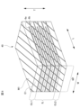
- FIG. 4 is a diagram showing a cross section taken along line III-III in FIG. 1.
- FIG. 4 shows an LW cross section of multilayer ceramic capacitor 1. The distribution of additive concentration on the LW surface of multilayer ceramic capacitor 1 will be explained.
- Line L1 shown in Fig. 4 indicates a position 60 ⁇ m from the end of the inner layer portion 10 on the second end face E2 side toward the first end face E1. That is, distance D1 shown in Fig. 4 is 60 ⁇ m.
- region R2 the region between the end of the inner layer portion 10 on the second end face E2 side and line L1 is region R2.
- the end of the inner layer portion 10 on the second end face E2 side is the interface between the inner layer portion 10 and the second dielectric layer 5b.
- Line L2 shown in Fig. 4 indicates a position 60 ⁇ m from the end of the inner layer portion 10 on the second side surface S2 side toward the first side surface S1. That is, distance D2 shown in Fig. 4 is 60 ⁇ m.
- region R5 the region between the end of the inner layer portion 10 on the second side surface S2 side and line L2 is region R5.
- the end of the inner layer portion 10 on the second side surface S2 side is the interface between the inner layer portion 10 and the second dielectric layer 5b.
- Region R1 is a region from the end of the inner layer portion 10 on the first end face E1 side to a line indicating a position 60 ⁇ m in the direction of the second end face E2.
- Region R4 is a region from the end of the inner layer portion 10 on the first side face S1 side to a line indicating a position 60 ⁇ m in the direction of the second side face S2.
- Line L3 shown in FIG. 4 is the center line of the inner layer 10 in the length direction L.
- Line L4 is the center line of the inner layer 10 in the width direction W.
- a region R3 is a range having a length of 60 ⁇ m in the longitudinal direction L, centered on the line L3.
- a region R6 is a range having a length of 60 ⁇ m in the width direction W, centered on the line L4.
- the additive concentration in region R2 is higher than the additive concentration in region R3.
- the concentration of the additive in region R5 is higher than the concentration of the additive in region R6.
- region R7 the region where region R2 and region R5 overlap is referred to as region R7.
- the additive concentration in region R7 is higher than the additive concentration in region R2 and the additive concentration in region R5.
- Region R7 has the highest additive concentration, so the movement of electrons can be further suppressed. This makes it possible to suppress insulation deterioration and insulation breakdown at the intersection of the end face side and the side end of the inner layer portion 10, where the electric field is likely to concentrate.
- the external electrodes include a first external electrode 20a and a second external electrode 20b.
- the first external electrode 20a is connected to the first internal electrode layer 6a.
- the first external electrode 20a is disposed from the first end face E1 to a part of the first main face M1 and a part of the second main face M2, as well as a part of the first side face S1 and a part of the second side face S2.
- the second external electrode 20b is connected to the second internal electrode layer 6b.
- the second external electrode 20b is also disposed on a portion of the first main surface M1 and a portion of the second main surface M2 from the second end face E2, as well as a portion of the first side surface S1 and a portion of the second side surface S2.
- the first external electrode 20a and the second external electrode 20b preferably have a base electrode layer and a plating layer.
- the base electrode layer may include at least one selected from a baked layer, a conductive resin layer, a thin film layer, and the like.
- the conductive resin layer may also be provided separately from the base electrode layer. In the following explanation, an example is given of a configuration that includes a baked layer as the base electrode layer, and a conductive resin layer in addition to the base electrode layer.
- the first external electrode 20a includes a first base electrode layer 21a, a first conductive resin layer 22a, a first lower plating layer 23a, and a first upper plating layer 24a.
- the second external electrode 20b includes a second base electrode layer 21b, a second conductive resin layer 22b, a second lower plating layer 23b, and a second upper plating layer 24b.
- the first base electrode layer 21a and the second base electrode layer 21b are layers containing conductive metal and glass components.
- the first conductive resin layer 22a and the second conductive resin layer 22b are layers made of thermosetting resin without containing metal components.
- the first lower plating layer 23a and the second lower plating layer 23b can be, for example, Ni plating layers.
- the first upper plating layer 24a and the second upper plating layer 24b can be, for example, Sn plating layers. Each layer will be described in turn below.
- the base electrode layer includes a first base electrode layer 21a and a second base electrode layer 21b.
- the first base electrode layer 21a is disposed from the first end face E1 to a part of the first main surface M1 and a part of the second main surface M2, as well as a part of the first side surface S1 and a part of the second side surface S2.
- the second base electrode layer 21b is disposed from the second end face E2 to a part of the first main surface M1 and a part of the second main surface M2, as well as a part of the first side surface S1 and a part of the second side surface S2.
- the first base electrode layer 21a and the second base electrode layer 21b contain a conductive metal and a glass component.
- the conductive metal contains at least one selected from, for example, Cu, Ni, Ag, Pd, Ag-Pd alloy, Au, etc.
- the glass component contains at least one selected from, for example, B, Si, Ba, Mg, Al, Li, etc.
- the first base electrode layer 21a and the second base electrode layer 21b may each be formed as a multi-layer structure.
- the first base electrode layer 21a and the second base electrode layer 21b may be formed by applying a conductive paste containing a glass component and a metal to the laminate and baking it. This baking may be performed simultaneously with the baking of the internal electrode layer, or may be performed after the baking of the internal electrode layer. When baking is performed simultaneously with the baking of the internal electrode layer and the dielectric layer, it is preferable to add a dielectric material instead of the glass component to form the base electrode layer by baking. In this way, the first base electrode layer 21a and the second base electrode layer 21b are configured as baked layers.
- the thickness of the first base electrode layer 21a at the center of the stacking direction T of the first base electrode layer 21a located on the first end face E1 is preferably, for example, about 10 ⁇ m or more and 150 ⁇ m or less.
- the thickness of the second base electrode layer 21b at the center of the stacking direction T of the second base electrode layer 21b located on the second end face E2 is preferably, for example, about 10 ⁇ m or more and 150 ⁇ m or less.
- the thickness of the first and second underlying electrode layers 21a and 21b at the center in the length direction L of the first and second underlying electrode layers 21a and 21b located on the first and second main surfaces M1 and M2, and the first and second side surfaces S1 and S2 is, for example, about 5 ⁇ m or more and 50 ⁇ m or less.
- the thin film layer can be formed by a thin film formation method such as sputtering or vapor deposition.
- the formed thin film layer is a layer of metal particles deposited to a thickness of 1 ⁇ m or less.
- a conductive resin layer is disposed on the base electrode layer.
- the conductive resin layer contains a resin component and a metal component.
- the conductive resin layer has a first conductive resin layer 22a and a second conductive resin layer 22b.
- the first conductive resin layer 22a and the second conductive resin layer 22b contain a thermosetting resin, which is a resin component. Therefore, the first conductive resin layer 22a and the second conductive resin layer 22b are more flexible than the base electrode layer. This is because the base electrode layer is made of, for example, a plating film or a fired product of a metal component and a glass component.
- thermosetting resin contained in the conductive resin layer include various known thermosetting resins such as epoxy resin, phenolic resin, urethane resin, silicone resin, and polyimide resin.
- epoxy resin is one of the most suitable resins. This is because epoxy resin has excellent heat resistance, moisture resistance, and adhesion.
- the first conductive resin layer 22a is disposed on the first base electrode layer 21a.
- the first conductive resin layer 22a is disposed so as to cover the first base electrode layer 21a.
- the end of the first conductive resin layer 22a is preferably in contact with the laminate 2.
- the second conductive resin layer 22b is disposed on the second base electrode layer 21b.
- the second conductive resin layer 22b is disposed so as to cover the second base electrode layer 21b.
- the end of the second conductive resin layer 22b is preferably in contact with the laminate 2.
- the metal components contained in the first conductive resin layer 22a and the second conductive resin layer 22b can be Ag, Cu, Ni, Sn, Bi, or an alloy containing these.
- the metal components are preferably formed in the form of a metal filler.
- metal powders metal powders whose surfaces are coated with Sn, Ni, or Cu can also be used.
- Ag may be Ag alone, an alloy containing Ag, or a metal powder whose surface is coated with Ag.
- the metal powder When using metal powder with an Ag-coated surface, it is preferable to use Cu, Ni, Sn, Bi or an alloy powder of these metals as the metal powder.
- Ag When Ag is used as the metal filler, there are the following advantages. Ag has the lowest resistivity of all metals. Therefore, electrodes with low electrical resistance can be formed. Because Ag is a precious metal, it is difficult to oxidize. Therefore, the resistance of the conductive resin layer can be increased. As described above, by using Ag as the metal filler, the base metal can be made inexpensive while maintaining the properties of Ag.
- the shape of the metal filler contained in the first conductive resin layer 22a and the second conductive resin layer 22b is not particularly limited.
- the shape of the metal filler may be spherical, flat, etc.
- the metal filler may be a mixture of spherical metal powder and flat metal powder.
- the average particle size of the metal filler contained in the first conductive resin layer 22a and the second conductive resin layer 22b is not particularly limited.
- the average particle size of the metal filler can be, for example, 0.3 ⁇ m or more and 10 ⁇ m or less.
- the average particle size of the metal filler contained in the conductive resin layer can be calculated using a laser diffraction particle size measurement method (based on IOS 13320). This method of calculating the average particle size can be applied regardless of the shape of the filler.
- the metal fillers contained in the first conductive resin layer 22a and the second conductive resin layer 22b are mainly responsible for the electrical conductivity of the conductive resin layers. Specifically, when the metal fillers come into contact with each other, an electrical path is formed inside the conductive resin layers.
- examples of the resin contained in the first conductive resin layer 22a and the second conductive resin layer 22b include various known thermosetting resins such as epoxy resin, phenoxy resin, phenolic resin, urethane resin, silicone resin, and polyimide resin.
- thermosetting resins such as epoxy resin, phenoxy resin, phenolic resin, urethane resin, silicone resin, and polyimide resin.
- epoxy resin which has excellent heat resistance, moisture resistance, and adhesion, is one of the most suitable resins.
- the first conductive resin layer 22a and the second conductive resin layer 22b preferably contain a hardener in addition to the thermosetting resin.
- a hardener in addition to the thermosetting resin.
- various known compounds such as phenol-based, amine-based, acid anhydride-based, imidazole-based, active ester-based, and amide-imide-based compounds can be used as the hardener.
- the metal contained in the first conductive resin layer 22a is preferably contained in an amount of 35 vmol% or more and 75 vmol% or less relative to the total volume of the first conductive resin layer 22a.
- the metal contained in the second conductive resin layer 22b is preferably contained in an amount of 35 vmol% or more and 75 vmol% or less relative to the total volume of the second conductive resin layer 22b.
- the resin contained in the first conductive resin layer 22a is preferably contained in an amount of 25 vmol% or more and 65 vmol% or less with respect to the total volume of the first conductive resin layer 22a.
- the resin contained in the second conductive resin layer 22b is preferably contained in an amount of 25 vmol% or more and 65 vmol% or less with respect to the total volume of the second conductive resin layer 22b.
- the thickness of the first conductive resin layer 22a or the second conductive resin layer 22b located at the center in the stacking direction T of the first end face E1 or the second end face E2 is preferably, for example, about 10 ⁇ m or more and 200 ⁇ m or less.
- the thickness of the conductive resin layer at the center in the length direction L of the first conductive resin layer 22a or the second conductive resin layer 22b located on the first main surface M1 and the second main surface M2, and the first side surface S1 and the second side surface S2 is preferably, for example, about 10 ⁇ m or more and 200 ⁇ m or less.
- the plating layer includes a lower plating layer and an upper plating layer. That is, the plating layer includes two layers. However, the plating layer may be a single layer or multiple layers.
- the lower-layer plating layer is disposed on the conductive resin layer.
- the lower-layer plating layer covers at least a portion of the conductive resin layer.
- the lower-layer plating layer includes a first lower-layer plating layer 23a and a second lower-layer plating layer 23b.
- the first lower-layer plating layer 23a is disposed on the first conductive resin layer 22a.
- the second lower-layer plating layer 23b is disposed on the second conductive resin layer 22b.
- the first underlayer plating layer 23a and the second underlayer plating layer 23b can be Ni plating layers. By using Ni plating layers as the underlayer plating layers, it is possible to prevent the underlayer electrode layer and the like from being eroded by solder when mounting the multilayer ceramic capacitor 1.
- the upper layer plating layer is disposed on the lower layer plating layer.
- the upper layer plating layer covers at least a portion of the lower layer plating layer.
- the upper layer plating layer includes a first upper layer plating layer 24a and a second upper layer plating layer 24b.
- the first upper layer plating layer 24a is disposed on the first lower layer plating layer 23a.
- the second upper layer plating layer 24b is disposed on the second lower layer plating layer 23b.
- the first upper plating layer 24a and the second upper plating layer 24b can be Sn plating layers. Sn plating layers have good solder wettability. Therefore, by using a Sn plating layer for the upper plating layer, mounting of the multilayer ceramic capacitor 1 on a substrate or the like can be made easier.
- the metals that are the materials for the lower plating layer and the upper plating layer are not limited to the above examples.
- the plating layers, including the lower plating layer and the upper plating layer can contain at least one selected from metals such as Cu, Ni, Ag, Pd, Au, and Sn, and alloys such as Ag-Pd alloys.
- each plating layer is 2 ⁇ m or more and 15 ⁇ m or less.
- External electrodes can also be formed using only the plating layer, without providing a base electrode layer.
- External electrodes can also be formed using only the plating layer, without providing a base electrode layer. Below, we will explain a structure in which only the plating layer is provided, without providing a base electrode layer.
- Each of the first external electrode 20a and the second external electrode 20b is formed as a plating layer directly on the surface of the laminate 2. That is, the multilayer ceramic capacitor 1 may have a structure including a plating layer electrically connected to the first internal electrode layer 6a or the second internal electrode layer 6b. When the external electrodes have such a structure, a plating layer may be formed after a catalyst is placed on the surface of the laminate 2 as a pretreatment.
- the plating layer preferably includes a lower layer plating electrode formed on the surface of the laminate 2, and an upper layer plating electrode formed on the surface of the lower layer plating electrode.
- the lower layer plating electrode and the upper layer plating electrode each include at least one metal selected from, for example, Cu, Ni, Sn, Pb, Au, Ag, Pd, Bi, or Zn, or an alloy containing the metal.
- the lower layer plated electrode is preferably formed using Ni, which has solder barrier properties.
- the upper layer plated electrode is preferably formed using Sn or Au, which have good solder wettability.
- the lower layer plating electrode is formed using Cu, which has good bonding properties with Ni.
- the upper layer plating electrode may be formed as necessary, and the first external electrode 20a and the second external electrode 20b may each be composed of only the lower layer plating electrode.
- the plating layer may have an upper plating electrode as the outermost layer, or another plating electrode may be formed on the surface of the upper plating electrode.
- the thickness of each plating layer is preferably 1 ⁇ m or more and 15 ⁇ m or less.
- the plating layer does not contain glass.
- the metal ratio per unit volume of the plating layer is preferably 99 volume % or more.
- the dimensions of the multilayer ceramic capacitor 1 are not particularly limited.
- the dimension in the length direction L of the multilayer ceramic capacitor 1, including the laminate 2 and the external electrodes, is defined as the L dimension.
- the L dimension is preferably 0.2 mm or more and 10 mm or less.
- the dimension in the stacking direction T of the multilayer ceramic capacitor 1, including the laminate 2 and the external electrodes, is defined as the T dimension.
- the T dimension is preferably 0.1 mm or more and 0.5 mm or less.
- the dimension in the width direction of the multilayer ceramic capacitor 1, including the laminate 2 and the external electrodes, is defined as the W dimension.
- the W dimension is preferably 0.1 mm or more and 10 mm or less.
- the conductive paste for the dielectric sheet and the internal electrode layer contains a binder and a solvent.
- Known organic binders and organic solvents can be used as the binder and the solvent.
- a conductive paste for the internal electrode layer is printed in a predetermined pattern on the dielectric sheet to form an internal electrode layer pattern.
- the printing can be performed by, for example, screen printing or gravure printing.
- a predetermined number of dielectric sheets for the outer layer are stacked.
- the dielectric sheets for the outer layer do not have an internal electrode layer pattern printed on them.
- Dielectric sheets with internal electrode layer patterns printed on them are stacked in sequence on top of them.
- a predetermined number of dielectric sheets for the outer layer are stacked on top of them. This produces a laminated sheet.
- the second dielectric layer 5b for reducing the step is described below.
- the dielectric paste that becomes the second dielectric layer 5b is called the step reduction paste.
- the step-reducing paste is applied to the area surrounding the pattern for the internal electrode layer on a dielectric sheet on which an internal electrode layer pattern has been formed by printing a conductive paste for the internal electrode layer. That is, the step-reducing paste is applied to the area on which the pattern for the internal electrode layer is not formed. This is because the step-reducing paste is a paste used to eliminate the step between the pattern for the internal electrode layer and its surrounding area.
- the step-reducing paste can also be applied so that a portion of it overlaps the surrounding area of the pattern for the internal electrode layer. In this case, the overlap width can be, for example, about 50 ⁇ m.
- the step-reducing paste can also be applied so that a gap is formed between the pattern for the internal electrode layer and the step-reducing paste. In this case, the gap width can be, for example, 50 ⁇ m.
- the amount by which the step reduction paste covers the internal electrode layer when printed i.e., the overlap amount
- the amount by which the step reduction paste covers the internal electrode layer when printed can be, for example, ⁇ 30 ⁇ m in the length direction L and +20 ⁇ m in the width direction W
- the thickness can be, for example, about 50% of the thickness of the pattern for the internal electrode layer or the Ni thickness.
- the amount of covering on the second dielectric layer 5b i.e., the overlap amount
- the thickness can be, for example, about 50% of the thickness of the pattern for the internal electrode layer or the Ni thickness.
- the step-reducing paste may be the same as the ceramic paste used when producing the dielectric sheet, or a different paste may be used.
- the step-reducing paste has a larger amount of V added than the ceramic paste used when producing the dielectric sheet.
- the large amount of V added to the step-reducing paste causes diffusion of V into the dielectric sheet.
- V can be added by adding V powder to the step-reducing paste when it is produced.
- V powder can also be added by increasing the amount of V added when the raw material is produced. It can also be added by, for example, printing the step-reducing paste on the dielectric sheet and then further printing V paste on the step-reducing paste.
- the laminated sheets are pressed in the stacking direction to produce a laminated block. Pressing is performed using a means such as a hydrostatic press.
- the laminated block is cut to a predetermined size. This cuts out laminated chips. At this time, the corners and edges of the laminated chips may be rounded. This rounding can be achieved by barrel polishing or the like.
- the laminated chip is fired. This produces a laminate.
- the firing temperature is preferably 900°C or higher and 1200°C or lower. The firing temperature can be changed depending on the materials of the dielectric and internal electrode layers.
- a conductive paste that will become the base electrodes is applied to both end surfaces of the laminate to form a base electrode layer.
- a baked layer is formed as the base electrode layer.
- the conductive paste is applied to a predetermined position of the laminate.
- the conductive paste contains a glass component and a metal.
- the application can be performed by a method such as dipping.
- a baking process is performed to form the base electrode layer.
- the temperature of the baking process at this time is preferably 700°C or higher and 900°C or lower.
- the conductive resin layer is formed on the base electrode layer.
- the method of forming the conductive resin layer involves first preparing a conductive resin paste containing a resin component and a metal component. This conductive resin paste is applied onto the base electrode layer. This application can be performed by a dipping method. After application, heat treatment is performed at a temperature of 200°C or higher and 550°C or lower. This heat treatment thermally hardens the resin. This forms the conductive electrode layer.
- the atmosphere during the heat treatment is preferably a nitrogen gas atmosphere.
- Ni plating layers are formed on the surface of the conductive resin layer as a first underlayer plating layer and a second underlayer plating layer.
- An electrolytic plating method can be used as a method for forming the first Ni plating layer and the second Ni plating layer.
- barrel plating it is preferable to use barrel plating as the plating method.
- a Sn plating layer is further formed on the Ni plating layer. That is, a first Sn plating layer is formed on the first Ni plating layer, and a second Sn plating layer is formed on the second Ni plating layer.
- An electrolytic plating method can be used as a method for forming the Sn plating layer. In addition, it is preferable to use barrel plating as the plating method.
- the concentration of the additive at the ends of the inner layer 10 is made higher than the concentration of the additive at the center of the inner layer 10.
- the method of making the additive concentration at the ends of the inner layer portion 10 higher than the additive concentration at the center of the inner layer portion 10 is not limited to the method of using a step-reducing paste. Even if a step-reducing paste is not used, the additive concentration at the ends of the inner layer portion 10 can be made higher than the additive concentration at the center of the inner layer portion 10. The case where a step-reducing paste is not used corresponds to the case where the second dielectric layer 5b is not provided.
- the second dielectric layer 5b is not provided, for example, a method can be used in which an additive or a material containing an additive is applied to the area of the dielectric sheet where the step reduction paste is printed.
- an additive or a material containing an additive is applied to the area surrounding the pattern for the internal electrode layer in the dielectric sheet.
- the second dielectric layer 5b is not limited to being provided both near the end face and near the side face.
- the second dielectric layer 5b can also be provided either near the end face or near the side face.
- an additive or a material containing an additive is applied to the corresponding portion of the dielectric sheet. This makes it possible to make the concentration of the additive at the end of the inner layer portion 10 higher than the concentration of the additive at the center of the inner layer portion 10.
- the multilayer ceramic capacitor 1 of the second embodiment differs from the multilayer ceramic capacitor 1 of the first embodiment in that the side surface outer layer portion is formed by a dielectric sheet for the side surface outer layer portion.
- the first side surface outer layer portion WG1 is referred to as the first side surface outer layer portion 30a
- the second side surface outer layer portion WG2 is referred to as the second side surface outer layer portion 30b.
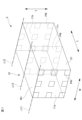
- FIG. 5 is a diagram corresponding to the cross-sectional view of line II-II in FIG. 1 in the second embodiment.
- the laminate 2 includes a laminate core portion 40, a first side surface side outer layer portion 30a, and a second side surface side outer layer portion 30b.
- the laminate core portion 40 is a portion of the laminate 2 that corresponds to the W-facing portion WF.
- the first side surface side outer layer portion 30a and the second side surface side outer layer portion 30b are provided to sandwich the laminate core portion 40.
- FIG. 6 is a diagram showing an overview of the laminate core part 40.
- the first internal electrode layer 6a and the second internal electrode layer 6b are exposed from the two end faces in the width direction W of the laminate core part 40.
- the side outer layer portion can be made of a dielectric material having a perovskite structure mainly composed of BaTiO 3 , for example.
- the mole number of Si/mol number of Ti in the side outer layer portion is preferably 1.0 or more and 7.0 or less.
- the steps (1) to (4) in the manufacturing method of the first embodiment can be similarly used.
- the laminated block is cut so that the conductive paste corresponding to the internal electrode layers is exposed on both sides in the width direction W.
- the conductive paste for the internal electrode layers is printed on the dielectric sheets in a pattern that enables such cutting.
- a dielectric sheet for the outer layer on the side is prepared. Specifically, a perovskite compound containing Ba and Ti is prepared as the dielectric material. At least one of Si, Mg, Ni, and Ba is added as an additive to the dielectric powder obtained from this dielectric material. Furthermore, V is added as an additive. A binder resin, an organic solvent, a plasticizer, and a dispersant are mixed with the dielectric powder in a predetermined ratio. This produces a ceramic slurry.
- the solvent contained in the ceramic slurry that forms the inner layer of the outer side portion is appropriately selected to be optimal in order to prevent dissolution of the dielectric sheet for the outer layer.
- This dielectric sheet for the inner layer also serves to adhere to the laminated chip.
- the V content of the additive contained in the inner layer is preferably greater than the V content of the additive contained in the outer layer.
- the ceramic slurry that will become the inner layer is applied to the surface of the dielectric sheet for the outer layer and dried. This forms a dielectric sheet for the inner layer. In this way, a dielectric sheet for the outer layer on the side having a two-layer structure is obtained.
- the dielectric sheet for the outer layer portion of the side surface of the two-layer structure is obtained by applying the dielectric sheet for the inner layer portion to the surface of the dielectric sheet for the outer layer and drying it.
- the dielectric sheet for the outer layer and the dielectric sheet for the inner layer portion may each be formed in advance. Then, each of these may be bonded together to obtain the dielectric sheet for the outer layer portion of the side surface of the two-layer structure.
- the dielectric sheet for the outer layer portion of the side surface is not limited to two layers, and may be multiple layers of three or more layers.
- the dielectric sheet for the side outer layer portion is peeled off from the resin film such as the PET film. Then, the dielectric sheet for the inner layer of the peeled dielectric sheet for the side outer layer portion is pressed against the laminated chip. At this time, the dielectric sheet is pressed against one side in the width direction W of the laminated chip. Then, by punching, a layer that will become the side outer layer portion is formed. Next, similarly, the dielectric sheet for the inner layer portion is opposed and pressed against the other side of the laminated chip on which the layer that will become the side outer layer portion is not formed. Then, by punching, a layer that will become the side outer layer portion is formed. At this time, it is preferable to apply an organic solvent that will serve as an adhesive to the side of the laminated chip in advance.
- the laminated chip on which the layer that will become the outer side layer is formed is degreased under specified conditions in a nitrogen atmosphere.
- the laminated chip is then fired at a specified temperature in a nitrogen-hydrogen-water vapor mixed atmosphere to obtain a sintered laminate.
- a second dielectric layer 5b for reducing steps can be disposed near the end faces of the laminate, as in the first embodiment. Also, the material constituting the second dielectric layer 5b can contain a large amount of additives, as in the first embodiment.
- the second dielectric layer 5b may not be disposed near the end face of the laminate.
- a method of applying an additive or a material containing an additive to the area of the dielectric sheet where the step reduction paste is printed can be used.
- the additive concentration at the end of the inner layer 10 can be made higher than the additive concentration at the center of the inner layer 10. This is because the additive contained in the side outer layer, particularly the additive contained in the first inner layer 31a and the second inner layer 31b, diffuses into the dielectric layer of the inner layer 10.
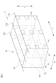
- Fig. 7 is a perspective view showing the polished inner layer portion 10.
- the laminate 2 is polished from the first end face E1 to a position 60 ⁇ m from the end of the inner layer portion 10 in the longitudinal direction L. This position is indicated by a line L11.
- the WT cross section at the line L11 is defined as a first cross section 11a.
- the laminate 2 is polished from the second end face E2 to a position 60 ⁇ m from the end of the inner layer portion 10 in the longitudinal direction L. This position is indicated by line L12.
- the WT cross section at line L12 is the second cross section 11b.
- the measurement area in the width direction W is 30 ⁇ m in one direction from the center position of the width direction W of the inner layer portion 10 in the width direction W and 30 ⁇ m in the other direction, i.e., a width of 60 ⁇ m in the width direction W centered on the center position, and a width of 60 ⁇ m from each end of the width direction W of the inner layer portion 10.
- the 60 ⁇ m width in the width direction W centered on the center position of the width direction W of the inner layer portion 10 is defined as the central portion in the width direction W.
- the measurement locations in the stacking direction T are 30 ⁇ m in one direction of the stacking direction T from the center position of the stacking direction T of the inner layer portion 10 and 30 ⁇ m in the other direction, i.e., a width of 60 ⁇ m in the stacking direction T centered on the center position, and a width of 60 ⁇ m from each end of the stacking direction T of the inner layer portion 10.
- the 60 ⁇ m width in the stacking direction T centered on the center position of the stacking direction T of the inner layer portion 10 is defined as the central portion in the stacking direction T.
- the inner layer 10 is further polished from the first cross section 11a or the second cross section 11b. Polishing is performed up to a position that is 1/2 the length of the inner layer 10 in the longitudinal direction L. This position is indicated by line L13.
- the WT cross section at line L13 is the third cross section 11c.
- the same areas as the first cross section 11a and the second cross section 11b are used as measurement areas.
- measurement sites PW The measurement sites determined in the above manner are referred to as measurement sites PW. There are 27 measurement sites PW in total, nine on each of the first cross section 11a, the second cross section 11b, and the third cross section 11c.
- the size of the area measured at each measurement site is 60 ⁇ m in both the width direction W and the stacking direction T.
- the length of one side of the rectangular area shown at the measurement site PW is 60 ⁇ m.
- LT surface Measurement on the LT surface will be described with reference to Fig. 8.
- Fig. 8 is a perspective view showing the polished inner layer portion 10.
- the measurement site is determined in the same manner as for the WT surface described above.
- the laminate 2 is polished from the first side surface S1 to a position 60 ⁇ m from the end of the inner layer portion 10 in the width direction W. This position is indicated by line L21.
- the LT cross section at line L21 is the fourth cross section 12a.
- the laminate 2 is polished from the second side surface S2 to a position 60 ⁇ m from the end of the inner layer portion 10 in the width direction W. This position is indicated by line L22.
- the LT cross section at line L22 is the fifth cross section 12b.
- the measurement points in the length direction L are 60 ⁇ m wide at the center of the inner layer 10 in the length direction L, and 60 ⁇ m wide from each end of the inner layer 10 in the length direction L.
- the measurement locations in the stacking direction T are a width of 60 ⁇ m at the center of the inner layer 10 in the stacking direction T, and a width of 60 ⁇ m from the end of the inner layer 10 in the stacking direction T.
- the inner layer 10 is further polished from the fourth cross section 12a or the fifth cross section 12b. Polishing is performed up to a position that is 1/2 the length of the width direction W of the inner layer 10. This position is indicated by line L23.
- the LT cross section at line L23 is designated as the sixth cross section 12c.
- the same positions are measured and positioned as in the fourth cross section 12a and the fifth cross section 12b.
- the measurements can be performed, for example, by measuring the WT surface as described above for 15 laminates 2 in one lot manufactured under the same conditions, and measuring the LT surface as described above for 15 laminates 2 in one lot manufactured under the same conditions.
- the concentration of additives on the end and side faces of the inner layer 10 is higher than the concentration of additives in the center of the inner layer 10. This makes it possible to further suppress the occurrence of insulation deterioration and insulation breakdown at the ends of the inner layer 10, where electric fields tend to concentrate.
- the concentration of the additive contained on the first side surface side of the inner layer portion is 100.1 mol % or more and 103.0 mol % or less of the concentration of the additive at the central portion in the width direction of the inner layer portion
- a concentration of the additive contained in the second side surface side of the inner layer portion is 100.1 mol % or more and 103.0 mol % or less of the concentration of the additive in a central portion in the width direction of the inner layer portion
- a concentration of the additive at an end of the second internal electrode layer on the first end face side of the internal layer portion is 100.1 mol % or more and 103.0 mol % or less of the concentration of the additive at a central portion in the length direction of the internal layer portion
- the range in which the concentration of the additive is highest is a range from an end portion on the first side surface side of the inner layer portion to a center portion in the width direction of 0 ⁇ m or more and 60 ⁇ m or less
- the multilayer ceramic electronic component according to ⁇ 1> or ⁇ 2>, wherein the range in which the concentration of the additive is highest is a range from 0 ⁇ m to 60 ⁇ m from an end portion on the second side surface side of the inner layer portion to a center portion in the width direction.
- ⁇ 4> The range in which the concentration of the additive is highest is a range from 0 ⁇ m to 60 ⁇ m from an end of the second internal electrode layer on the first end face side of the internal layer portion toward a center portion in the length direction
- ⁇ 4> The multilayer ceramic electronic component according to any one of ⁇ 1> to ⁇ 3>, wherein a range in which the concentration of the additive is highest is a range from an end of the first internal electrode layer on the second end face side of the inner layer portion toward a center portion in the longitudinal direction of the inner layer portion, the range being 0 ⁇ m or more and 60 ⁇ m or less.
- the laminate has an outer layer portion made of a dielectric material,
- the outer layer portion is a first main surface side outer layer portion located on the first main surface side and located between the first main surface and an outermost surface of the inner layer portion on the first main surface side in the stacking direction; a second main surface side outer layer portion located on the second main surface side and between the second main surface and an outermost surface of the inner layer portion on the second main surface side in the stacking direction; a first end face side outer layer portion located on the first end face side and located between an outermost surface on the first end face side and an outermost surface of an end portion of the second internal electrode layer that is not connected to the first external electrode; a second end face side outer layer portion located on the second end face side and located between an outermost surface on the second end face side and an outermost surface of an end portion of the first internal electrode layer that is not connected to the second external electrode; having The multilayer ceramic electronic component according to ⁇ 1>, further comprising a side surface outer layer portion disposed on a portion of the first end
- the side surface outer layer portion has an outer layer located near the first side surface and the second side surface, and an inner layer located more inward in the width direction than the outer layer, the Si content in the outer layer is greater than the Si content in the inner layer;
- ⁇ 8> The multilayer ceramic electronic component according to any one of ⁇ 5> to ⁇ 7>, wherein the dimension of the lateral outer layer portion along the width direction is 5 ⁇ m or more and 40 ⁇ m or less.
- the dielectric layer includes a first dielectric layer and a second dielectric layer; the first dielectric layer is disposed between the first internal electrode layer and the second internal electrode layer, the second dielectric layer is disposed so as to overlap the first dielectric layer in the stacking direction, including a region between the first dielectric layers opposed to each other via the internal electrode layer, in which the internal electrode layer is not disposed, and a part of the region is disposed so as to overlap the first dielectric layer in the stacking direction,
- the multilayer ceramic electronic component according to any one of ⁇ 1> to ⁇ 8>, wherein the second dielectric layer is disposed on at least a portion of the first side surface side outer layer portion, the second side surface side outer layer portion, the first end surface side outer layer portion, and the second end surface side outer layer portion.
- Multilayer ceramic capacitors (multilayer ceramic electronic components) 2 Laminate 3 Outer dielectric layer 4 Inner dielectric layer 10 Inner layer portion 40 Laminate core portion IL Inner layer range OL1 First main surface side outer layer portion OL2 Second main surface side outer layer portion LF L facing portion LG1 First end surface side outer layer portion LG2 Second end surface side outer layer portion WF W facing portion WG1 (30a) First side surface side outer layer portion WG2 (30b) Second side surface side outer layer portion
Landscapes
- Engineering & Computer Science (AREA)
- Power Engineering (AREA)
- Manufacturing & Machinery (AREA)
- Microelectronics & Electronic Packaging (AREA)
- Chemical & Material Sciences (AREA)
- Ceramic Engineering (AREA)
- Inorganic Chemistry (AREA)
- Materials Engineering (AREA)
- Ceramic Capacitors (AREA)
- Fixed Capacitors And Capacitor Manufacturing Machines (AREA)
Priority Applications (4)
| Application Number | Priority Date | Filing Date | Title |
|---|---|---|---|
| CN202480038895.XA CN121285868A (zh) | 2023-07-19 | 2024-05-08 | 层叠陶瓷电子部件 |
| KR1020257038618A KR20250170137A (ko) | 2023-07-19 | 2024-05-08 | 적층 세라믹 전자부품 |
| EP24842802.1A EP4730378A1 (en) | 2023-07-19 | 2024-05-08 | Multilayer ceramic electronic component |
| JP2025533876A JPWO2025018005A1 (https=) | 2023-07-19 | 2024-05-08 |
Applications Claiming Priority (2)
| Application Number | Priority Date | Filing Date | Title |
|---|---|---|---|
| JP2023117662 | 2023-07-19 | ||
| JP2023-117662 | 2023-07-19 |
Publications (1)
| Publication Number | Publication Date |
|---|---|
| WO2025018005A1 true WO2025018005A1 (ja) | 2025-01-23 |
Family
ID=94281434
Family Applications (1)
| Application Number | Title | Priority Date | Filing Date |
|---|---|---|---|
| PCT/JP2024/017064 Pending WO2025018005A1 (ja) | 2023-07-19 | 2024-05-08 | 積層セラミック電子部品 |
Country Status (5)
| Country | Link |
|---|---|
| EP (1) | EP4730378A1 (https=) |
| JP (1) | JPWO2025018005A1 (https=) |
| KR (1) | KR20250170137A (https=) |
| CN (1) | CN121285868A (https=) |
| WO (1) | WO2025018005A1 (https=) |
Citations (11)
| Publication number | Priority date | Publication date | Assignee | Title |
|---|---|---|---|---|
| JP2001267173A (ja) | 2000-03-17 | 2001-09-28 | Murata Mfg Co Ltd | 積層セラミックコンデンサ |
| JP2006001961A (ja) * | 2004-06-15 | 2006-01-05 | Tdk Corp | ホットメルトコーティング用誘電体塗料組成物およびその製造方法 |
| JP2009016796A (ja) * | 2007-06-08 | 2009-01-22 | Murata Mfg Co Ltd | 積層セラミック電子部品 |
| JP2016136557A (ja) * | 2015-01-23 | 2016-07-28 | Tdk株式会社 | 積層型セラミック電子部品 |
| JP2017011172A (ja) * | 2015-06-24 | 2017-01-12 | 太陽誘電株式会社 | 積層セラミックコンデンサ及びその製造方法 |
| JP2017038036A (ja) * | 2015-08-07 | 2017-02-16 | サムソン エレクトロ−メカニックス カンパニーリミテッド. | 積層セラミック電子部品及びその製造方法 |
| JP2018137286A (ja) * | 2017-02-20 | 2018-08-30 | 京セラ株式会社 | コンデンサ |
| JP2018182286A (ja) * | 2017-04-13 | 2018-11-15 | サムソン エレクトロ−メカニックス カンパニーリミテッド. | 積層セラミックキャパシター及びその実装基板 |
| JP2022068525A (ja) * | 2020-10-22 | 2022-05-10 | Tdk株式会社 | 積層セラミック電子部品 |
| JP2022133553A (ja) * | 2021-03-02 | 2022-09-14 | 太陽誘電株式会社 | 積層セラミックコンデンサ |
| WO2024038727A1 (ja) * | 2022-08-17 | 2024-02-22 | 太陽誘電株式会社 | 積層セラミック電子部品、および積層セラミック電子部品の製造方法 |
-
2024
- 2024-05-08 EP EP24842802.1A patent/EP4730378A1/en active Pending
- 2024-05-08 KR KR1020257038618A patent/KR20250170137A/ko active Pending
- 2024-05-08 WO PCT/JP2024/017064 patent/WO2025018005A1/ja active Pending
- 2024-05-08 CN CN202480038895.XA patent/CN121285868A/zh active Pending
- 2024-05-08 JP JP2025533876A patent/JPWO2025018005A1/ja active Pending
Patent Citations (11)
| Publication number | Priority date | Publication date | Assignee | Title |
|---|---|---|---|---|
| JP2001267173A (ja) | 2000-03-17 | 2001-09-28 | Murata Mfg Co Ltd | 積層セラミックコンデンサ |
| JP2006001961A (ja) * | 2004-06-15 | 2006-01-05 | Tdk Corp | ホットメルトコーティング用誘電体塗料組成物およびその製造方法 |
| JP2009016796A (ja) * | 2007-06-08 | 2009-01-22 | Murata Mfg Co Ltd | 積層セラミック電子部品 |
| JP2016136557A (ja) * | 2015-01-23 | 2016-07-28 | Tdk株式会社 | 積層型セラミック電子部品 |
| JP2017011172A (ja) * | 2015-06-24 | 2017-01-12 | 太陽誘電株式会社 | 積層セラミックコンデンサ及びその製造方法 |
| JP2017038036A (ja) * | 2015-08-07 | 2017-02-16 | サムソン エレクトロ−メカニックス カンパニーリミテッド. | 積層セラミック電子部品及びその製造方法 |
| JP2018137286A (ja) * | 2017-02-20 | 2018-08-30 | 京セラ株式会社 | コンデンサ |
| JP2018182286A (ja) * | 2017-04-13 | 2018-11-15 | サムソン エレクトロ−メカニックス カンパニーリミテッド. | 積層セラミックキャパシター及びその実装基板 |
| JP2022068525A (ja) * | 2020-10-22 | 2022-05-10 | Tdk株式会社 | 積層セラミック電子部品 |
| JP2022133553A (ja) * | 2021-03-02 | 2022-09-14 | 太陽誘電株式会社 | 積層セラミックコンデンサ |
| WO2024038727A1 (ja) * | 2022-08-17 | 2024-02-22 | 太陽誘電株式会社 | 積層セラミック電子部品、および積層セラミック電子部品の製造方法 |
Also Published As
| Publication number | Publication date |
|---|---|
| EP4730378A1 (en) | 2026-04-22 |
| CN121285868A (zh) | 2026-01-06 |
| JPWO2025018005A1 (https=) | 2025-01-23 |
| KR20250170137A (ko) | 2025-12-04 |
Similar Documents
| Publication | Publication Date | Title |
|---|---|---|
| US12224122B2 (en) | Electronic component, circuit board, and method of mounting electronic component on circuit board | |
| US20190157007A1 (en) | Electronic component mount structure, electronic component, and method for manufacturing electronic component | |
| US11062848B2 (en) | Multilayer ceramic electronic component | |
| US11361901B2 (en) | Multilayer ceramic electronic component with glass component, plating layer, and semiconductor layer | |
| JP2020155719A (ja) | 積層セラミックコンデンサ | |
| US12586716B2 (en) | Multilayer ceramic capacitor including internal electrode layers with varying coverages | |
| WO2024161743A1 (ja) | 積層セラミックコンデンサ | |
| JP2022129066A (ja) | 積層セラミックコンデンサ | |
| WO2025018005A1 (ja) | 積層セラミック電子部品 | |
| WO2025018007A1 (ja) | 積層セラミック電子部品 | |
| WO2024224760A1 (ja) | 積層セラミック電子部品 | |
| US20260128216A1 (en) | Multilayer ceramic electronic component | |
| WO2025088878A1 (ja) | 積層セラミック電子部品 | |
| JP2022163423A (ja) | 積層セラミックコンデンサ | |
| US20260128229A1 (en) | Multilayer ceramic capacitor | |
| KR20260053094A (ko) | 적층 세라믹 전자부품 | |
| US20250385045A1 (en) | Multilayer ceramic capacitor | |
| US20250054704A1 (en) | Multilayer ceramic electronic component and mounting structure of multilayer ceramic electronic component | |
| US20250054694A1 (en) | Multilayer ceramic electronic component | |
| WO2026069542A1 (ja) | 積層セラミック電子部品 | |
| CN121532842A (zh) | 层叠陶瓷电容器 | |
| JP2026058006A (ja) | 積層セラミック電子部品 | |
| CN121241414A (zh) | 层叠陶瓷电容器 | |
| JP2026054667A (ja) | 積層セラミックコンデンサ | |
| WO2025004490A1 (ja) | 積層セラミックコンデンサ |
Legal Events
| Date | Code | Title | Description |
|---|---|---|---|
| 121 | Ep: the epo has been informed by wipo that ep was designated in this application |
Ref document number: 24842802 Country of ref document: EP Kind code of ref document: A1 |
|
| ENP | Entry into the national phase |
Ref document number: 1020257038618 Country of ref document: KR Free format text: ST27 STATUS EVENT CODE: A-0-1-A10-A15-NAP-PA0105 (AS PROVIDED BY THE NATIONAL OFFICE) |
|
| WWE | Wipo information: entry into national phase |
Ref document number: KR1020257038618 Country of ref document: KR |
|
| ENP | Entry into the national phase |
Ref document number: 2025533876 Country of ref document: JP Kind code of ref document: A |
|
| WWE | Wipo information: entry into national phase |
Ref document number: 2025533876 Country of ref document: JP |
|
| WWE | Wipo information: entry into national phase |
Ref document number: 2024842802 Country of ref document: EP Ref document number: 202617004138 Country of ref document: IN |
|
| ENP | Entry into the national phase |
Ref document number: 2024842802 Country of ref document: EP Effective date: 20260115 |
|
| ENP | Entry into the national phase |
Ref document number: 2024842802 Country of ref document: EP Effective date: 20260115 |
|
| ENP | Entry into the national phase |
Ref document number: 2024842802 Country of ref document: EP Effective date: 20260115 |
|
| NENP | Non-entry into the national phase |
Ref country code: DE |
|
| WWP | Wipo information: published in national office |
Ref document number: 2024842802 Country of ref document: EP |