WO2025013468A1 - 半導体装置 - Google Patents
半導体装置 Download PDFInfo
- Publication number
- WO2025013468A1 WO2025013468A1 PCT/JP2024/020469 JP2024020469W WO2025013468A1 WO 2025013468 A1 WO2025013468 A1 WO 2025013468A1 JP 2024020469 W JP2024020469 W JP 2024020469W WO 2025013468 A1 WO2025013468 A1 WO 2025013468A1
- Authority
- WO
- WIPO (PCT)
- Prior art keywords
- conductive pattern
- output
- semiconductor device
- semiconductor
- semiconductor chip
- Prior art date
- Legal status (The legal status is an assumption and is not a legal conclusion. Google has not performed a legal analysis and makes no representation as to the accuracy of the status listed.)
- Ceased
Links
Images





Classifications
-
- H—ELECTRICITY
- H10—SEMICONDUCTOR DEVICES; ELECTRIC SOLID-STATE DEVICES NOT OTHERWISE PROVIDED FOR
- H10W—GENERIC PACKAGES, INTERCONNECTIONS, CONNECTORS OR OTHER CONSTRUCTIONAL DETAILS OF DEVICES COVERED BY CLASS H10
- H10W40/00—Arrangements for thermal protection or thermal control
- H10W40/20—Arrangements for cooling
- H10W40/25—Arrangements for cooling characterised by their materials
- H10W40/255—Arrangements for cooling characterised by their materials having a laminate or multilayered structure, e.g. direct bond copper [DBC] ceramic substrates
-
- H—ELECTRICITY
- H10—SEMICONDUCTOR DEVICES; ELECTRIC SOLID-STATE DEVICES NOT OTHERWISE PROVIDED FOR
- H10W—GENERIC PACKAGES, INTERCONNECTIONS, CONNECTORS OR OTHER CONSTRUCTIONAL DETAILS OF DEVICES COVERED BY CLASS H10
- H10W40/00—Arrangements for thermal protection or thermal control
- H10W40/20—Arrangements for cooling
- H10W40/25—Arrangements for cooling characterised by their materials
- H10W40/258—Metallic materials
-
- H—ELECTRICITY
- H10—SEMICONDUCTOR DEVICES; ELECTRIC SOLID-STATE DEVICES NOT OTHERWISE PROVIDED FOR
- H10W—GENERIC PACKAGES, INTERCONNECTIONS, CONNECTORS OR OTHER CONSTRUCTIONAL DETAILS OF DEVICES COVERED BY CLASS H10
- H10W42/00—Arrangements for protection of devices
- H10W42/60—Arrangements for protection of devices protecting against electrostatic charges or discharges, e.g. Faraday shields
-
- H—ELECTRICITY
- H10—SEMICONDUCTOR DEVICES; ELECTRIC SOLID-STATE DEVICES NOT OTHERWISE PROVIDED FOR
- H10W—GENERIC PACKAGES, INTERCONNECTIONS, CONNECTORS OR OTHER CONSTRUCTIONAL DETAILS OF DEVICES COVERED BY CLASS H10
- H10W70/00—Package substrates; Interposers; Redistribution layers [RDL]
- H10W70/60—Insulating or insulated package substrates; Interposers; Redistribution layers
- H10W70/62—Insulating or insulated package substrates; Interposers; Redistribution layers characterised by their interconnections
- H10W70/65—Shapes or dispositions of interconnections
- H10W70/658—Shapes or dispositions of interconnections for devices provided for in groups H10D8/00 - H10D48/00
-
- H—ELECTRICITY
- H10—SEMICONDUCTOR DEVICES; ELECTRIC SOLID-STATE DEVICES NOT OTHERWISE PROVIDED FOR
- H10W—GENERIC PACKAGES, INTERCONNECTIONS, CONNECTORS OR OTHER CONSTRUCTIONAL DETAILS OF DEVICES COVERED BY CLASS H10
- H10W72/00—Interconnections or connectors in packages
-
- H—ELECTRICITY
- H10—SEMICONDUCTOR DEVICES; ELECTRIC SOLID-STATE DEVICES NOT OTHERWISE PROVIDED FOR
- H10W—GENERIC PACKAGES, INTERCONNECTIONS, CONNECTORS OR OTHER CONSTRUCTIONAL DETAILS OF DEVICES COVERED BY CLASS H10
- H10W72/00—Interconnections or connectors in packages
- H10W72/50—Bond wires
-
- H—ELECTRICITY
- H10—SEMICONDUCTOR DEVICES; ELECTRIC SOLID-STATE DEVICES NOT OTHERWISE PROVIDED FOR
- H10W—GENERIC PACKAGES, INTERCONNECTIONS, CONNECTORS OR OTHER CONSTRUCTIONAL DETAILS OF DEVICES COVERED BY CLASS H10
- H10W90/00—Package configurations
-
- H—ELECTRICITY
- H10—SEMICONDUCTOR DEVICES; ELECTRIC SOLID-STATE DEVICES NOT OTHERWISE PROVIDED FOR
- H10W—GENERIC PACKAGES, INTERCONNECTIONS, CONNECTORS OR OTHER CONSTRUCTIONAL DETAILS OF DEVICES COVERED BY CLASS H10
- H10W72/00—Interconnections or connectors in packages
- H10W72/851—Dispositions of multiple connectors or interconnections
- H10W72/874—On different surfaces
- H10W72/884—Die-attach connectors and bond wires
-
- H—ELECTRICITY
- H10—SEMICONDUCTOR DEVICES; ELECTRIC SOLID-STATE DEVICES NOT OTHERWISE PROVIDED FOR
- H10W—GENERIC PACKAGES, INTERCONNECTIONS, CONNECTORS OR OTHER CONSTRUCTIONAL DETAILS OF DEVICES COVERED BY CLASS H10
- H10W90/00—Package configurations
- H10W90/701—Package configurations characterised by the relative positions of pads or connectors relative to package parts
- H10W90/731—Package configurations characterised by the relative positions of pads or connectors relative to package parts of die-attach connectors
- H10W90/734—Package configurations characterised by the relative positions of pads or connectors relative to package parts of die-attach connectors between a chip and a stacked insulating package substrate, interposer or RDL
-
- H—ELECTRICITY
- H10—SEMICONDUCTOR DEVICES; ELECTRIC SOLID-STATE DEVICES NOT OTHERWISE PROVIDED FOR
- H10W—GENERIC PACKAGES, INTERCONNECTIONS, CONNECTORS OR OTHER CONSTRUCTIONAL DETAILS OF DEVICES COVERED BY CLASS H10
- H10W90/00—Package configurations
- H10W90/701—Package configurations characterised by the relative positions of pads or connectors relative to package parts
- H10W90/751—Package configurations characterised by the relative positions of pads or connectors relative to package parts of bond wires
- H10W90/753—Package configurations characterised by the relative positions of pads or connectors relative to package parts of bond wires between laterally-adjacent chips
-
- H—ELECTRICITY
- H10—SEMICONDUCTOR DEVICES; ELECTRIC SOLID-STATE DEVICES NOT OTHERWISE PROVIDED FOR
- H10W—GENERIC PACKAGES, INTERCONNECTIONS, CONNECTORS OR OTHER CONSTRUCTIONAL DETAILS OF DEVICES COVERED BY CLASS H10
- H10W90/00—Package configurations
- H10W90/701—Package configurations characterised by the relative positions of pads or connectors relative to package parts
- H10W90/751—Package configurations characterised by the relative positions of pads or connectors relative to package parts of bond wires
- H10W90/754—Package configurations characterised by the relative positions of pads or connectors relative to package parts of bond wires between a chip and a stacked insulating package substrate, interposer or RDL
Definitions
- the present invention relates to a semiconductor device.
- the semiconductor device has a substrate including a circuit pattern on which semiconductor chips are arranged (see, for example, Patent Document 1).
- the semiconductor device is sealed with a sealing member (see, for example, Patent Documents 2 and 3).
- the semiconductor device further includes a heat sink on which multiple substrates on which semiconductor chips are arranged are arranged, and wiring members electrically connected to the conductive pattern of the substrate, which may be housed in a case (see, for example, Patent Document 4).
- the objective of the present invention is to provide a semiconductor device that ensures sufficient voltage resistance characteristics.
- a semiconductor device including: a first semiconductor chip including a control electrode provided on a side portion in a first direction on a front surface; an output conductive pattern including a rectangular first portion having sides extending in the first direction and a second direction perpendicular to the first direction, in which the first semiconductor chip is arranged; a second portion connected to the side of the first portion in the first direction and extending from a first side of the side in the first direction to a second side; an output terminal arranged on the second portion of the output conductive pattern; and a control conductive pattern including a connection portion electrically connected to the control electrode and adjacent to the second portion of the output conductive pattern on the opposite side to the first portion in a plan view, the second portion of the output conductive pattern having a recess adjacent to the first portion on the first side in a plan view and recessed from the first side toward the second side, and the connection portion of the control conductive pattern being provided in the recess.
- one output terminal may be provided, and the one output terminal may be disposed at a central portion of the width in the second direction of the second portion of the output conductive pattern. At least two of the output terminals may be provided, and the at least two output terminals may be arranged side by side in the second direction on the second portion of the output conductive pattern.
- the control electrode may be provided at the center of the side portion of the front surface of the first semiconductor chip.
- the width of the first semiconductor chip in the second direction may be less than half the width of the first portion of the output conductive pattern in the second direction, and two of the first semiconductor chips may be arranged side by side in the second direction in the first portion of the output conductive pattern.
- the first semiconductor chip may further include an output electrode provided on the front surface, and may further include a second semiconductor chip including a diode element arranged on the first portion of the output conductive pattern adjacent to the side of the first semiconductor chip opposite the second portion of the output conductive pattern, and the second semiconductor chip may be electrically connected to the output electrode of the first semiconductor chip and the first portion of the output conductive pattern.
- the width of the first semiconductor chip in the second direction may be less than or equal to the width of the first portion of the output conductive pattern in the second direction, and one first semiconductor chip may be disposed in the first portion of the output conductive pattern.
- the device may further include a wire connecting the connection portion of the control conductive pattern and the control electrode of the first semiconductor chip, and the shortest distance from the wire to the output terminal that is closest to the connection portion among the at least two output terminals in a plan view may be 1.5 mm or more.
- the first semiconductor chip may have a withstand voltage of 1200V.
- the first semiconductor chip may be an insulated gate bipolar transistor.
- the semiconductor device may further include a wire connecting the connection portion of the control conductive pattern and the control electrode of the first semiconductor chip, and the shortest distance from the wire to an output terminal of the at least two output terminals that is closest to the connection portion in a planar view may be 2.2 mm or more.
- the first semiconductor chip may have a withstand voltage of 1700V.
- the first semiconductor chip may be a reverse conducting insulated gate bipolar transistor.
- the control electrode may be provided on the first side or the second side of the center of the side portion of the front surface.
- the second portion of the output conductive pattern may include a coupling region that is electrically connected to another external output conductive pattern.
- the recess included in the second portion of the output conductive pattern may be U-shaped in a plan view with an opening facing the first side.
- the connecting region may also be included along the depression at an end of the depression on the first side.
- the recess included in the second portion of the output conductive pattern may be provided on the first side from the center of the width of the first portion of the output conductive pattern in the second direction.
- the recess included in the second portion of the output conductive pattern may be L-shaped in a plan view with an opening facing the first side and the first direction.
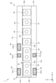
- FIG. 1 is a plan view of a semiconductor device.
- FIG. 2 is a side view of the semiconductor device.
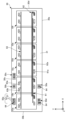
- FIG. 2 is a plan view of the semiconductor device according to the first embodiment (when the case is removed);
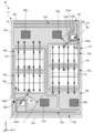
- 1 is a plan view of a semiconductor unit included in a semiconductor device according to a first embodiment;
- 2 is a plan view of an insulating circuit board included in the semiconductor device of the first embodiment;
- 2 is a cross-sectional view of an insulating circuit board included in the semiconductor device of the first embodiment.
- 1 is a plan view of a semiconductor unit included in a semiconductor device of a reference example.
- FIG. 13 is a plan view of the semiconductor device according to the second embodiment (when the case is removed);
- FIG. 13 is a plan view of the semiconductor device according to the second embodiment (when the case is removed);
- FIG. 13 is a plan view of a semiconductor unit included in a semiconductor device according to a second embodiment.
- FIG. 13 is a plan view of an insulating circuit board included in a semiconductor device according to a second embodiment.
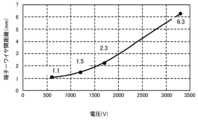
- 1 is a graph showing the terminal-to-wire distance required to suppress discharge versus voltage.
- FIG. 13 is a plan view of a semiconductor unit included in a semiconductor device according to a third embodiment.
- FIG. 13 is a plan view of a semiconductor unit included in a semiconductor device according to a fourth embodiment.
- front surface and “upper surface” refer to the X-Y surface facing upward (+Z direction) in the semiconductor device 1 in the figure.
- up refers to the upward (+Z direction) direction in the semiconductor device 1 in the figure.
- back surface and “lower surface” refer to the X-Y surface facing downward (-Z direction) in the semiconductor device 1 in the figure.
- lower refers to the downward (-Z direction) direction in the semiconductor device 1 in the figure.
- High position refers to the upper (+Z direction) position in the semiconductor device 1 in the figure.
- low position refers to the lower (-Z direction) position in the semiconductor device 1 in the figure.
- the terms “front surface”, “upper surface”, “upper” and “back surface”, “lower surface”, “lower” and “side surface” are merely convenient expressions for specifying relative positional relationships and do not limit the technical ideas of the present invention.
- “up” and “down” do not necessarily mean the vertical direction relative to the ground.
- the directions of “up” and “down” are not limited to the direction of gravity.
- main component refers to a component that contains 80 vol% or more. "Approximately the same” means within a range of ⁇ 10%.
- Perfectdicular”, “orthogonal” and “parallel” mean within a range of ⁇ 10°.
- Fig. 1 is a plan view of the semiconductor device.
- Fig. 2 is a side view of the semiconductor device.
- Fig. 3 is a plan view of the semiconductor device of the first embodiment (when the case is removed).
- Fig. 2 is a side view of the semiconductor device 1 of Fig. 1 as viewed in the +Y direction.
- Fig. 3 is a plan view of the semiconductor device 1 of Fig. 1 with the case 20 removed.
- the semiconductor unit included in the semiconductor device 1 is omitted.
- the semiconductor device 1 includes a case 20.
- the case 20 is attached to a heat dissipation base plate 30 to which the semiconductor units 10a to 10f are joined, as described below.
- the case 20 When the case 20 is attached to the heat dissipation base plate 30, it houses the semiconductor units 10a to 10f.
- Such a case 20 includes a lower storage section 21 and an upper storage section 22.
- the lower storage section 21 is shaped like a rectangular parallelepiped. In a plan view, the lower storage section 21 is surrounded on all four sides by long side walls 21a, short side walls 21b, long side walls 21c, and short side walls 21d.
- the lower storage section 21 also includes a lower front surface 21e in an opening surrounded by long side walls 21a, short side walls 21b, long side walls 21c, and short side walls 21d.
- the lower front surface 21e includes control terminal regions 21e1 to 21e5.
- Control terminal region 21e1 is provided on the edge of the long side wall 21c side, close to the short side wall 21b of the lower front surface 21e.
- Control terminal region 21e2 is provided on the edge of the long side wall 21c side of the lower front surface 21e, adjacent to the control terminal region 21e in the +X direction.
- Control terminal region 21e3 is provided on the edge of the long side wall 21c side of the lower front surface 21e, adjacent to the control terminal region 21e2 in the +X direction.
- Control terminal region 21e4 is provided on the edge of the long side wall 21a side, close to the short side wall 21b of the lower front surface 21e, facing the control terminal region 21e1.
- the control terminal area 21e5 is located on the edge of the long side wall 21a of the lower front surface 21e, next to the control terminal area 21e4 in the +X direction. Furthermore, the control terminal area 21e5 faces the control terminal area 21e2.
- control wiring member 64 is exposed.
- the connection portion at the tip of the wiring member 64 is exposed from the control terminal areas 21e1-21e5 and bent.
- the control terminal areas 21e1-21e5 may house a nut that faces the connection portion of the bent wiring member 64.
- the upper storage section 22 is provided on the lower front surface 21e of the lower storage section 21.
- the upper storage section 22 is also rectangular parallelepiped-shaped. In a plan view, the upper storage section 22 is surrounded on all four sides by long side walls 22a, short side walls 22b, long side walls 22c, and short side walls 22d.
- the upper storage section 22 includes the upper front surface 22e in an opening surrounded by the long side walls 22a, short side walls 22b, long side walls 22c, and short side walls 22d.
- the long side walls 22a, 22c may be the same length as the long side walls 21a, 21c of the lower storage section 21.
- the upper storage section 22 is provided integrally at the center of the lower front surface 21e of the lower storage section 21 in the ⁇ Y direction.
- the area of the lower front surface 21e of the lower storage section 21 where the upper storage section 22 is formed is open.
- the long side walls 22a, 22c are integrally connected to the lower front surface 21e of the lower storage section 21.
- the short side walls 22b, 22d are integrally connected to the short side walls 21b, 21d of the lower storage section 21 and form the same plane.
- output, output, positive electrode, negative electrode, positive electrode, negative electrode wiring members 63, 63, 61, 62, 61, 62 (connection portions) are provided from the short side wall 22b toward the short side wall 22d (along the +X direction).
- Output, output, positive electrode, negative electrode, positive electrode, negative electrode wiring members 63, 63, 61, 62, 61, 62 are also bent to face the upper front surface 22e.
- output wiring member 63 is bent in the -Y direction.
- Positive electrode, negative electrode, positive electrode, negative electrode wiring members 61, 62, 61, 62 are also bent in the -Y direction.
- the upper front surface 22e may also house nuts that face the connection portions of the bent wiring members 63, 63, 61, 62, 61, 62.
- the case 20 having the above configuration may be made of a thermoplastic resin.
- resins include polyphenylene sulfide resin, polybutylene terephthalate resin, polybutylene succinate resin, polyamide resin, and acrylonitrile butadiene styrene resin.
- the semiconductor device 1 includes a heat dissipating base plate 30, a plurality of semiconductor units 10a-10f provided on the heat dissipating base plate 30, control wiring units 50a-50e, and wiring members 61, 62, 63 for positive electrodes, negative electrodes, and output.
- the semiconductor units 10a-10f each have the same configuration. When there is no need to distinguish between the semiconductor units 10a-10f, they will be referred to as semiconductor unit 10. When there is no need to distinguish between the control wiring units 50a-50e, they will be referred to as control wiring unit 50. Details of the semiconductor unit 10 will be described later.
- the semiconductor device 1 has a case 20 attached to a heat dissipation base plate 30.
- the case 20 covers the semiconductor unit 10 on the heat dissipation base plate 30, the control wiring unit 50, and the wiring members 61, 62, and 63.
- the heat dissipating base plate 30 includes a rectangular upper surface 31 (see FIG. 3) and lower surface 32 (see FIG. 2) in a plan view, and long sides 30a, short sides 30b, long sides 30c, and short sides 30d surrounding the upper surface 31 on all four sides.
- the heat dissipating base plate 30 is made of a metal with excellent thermal conductivity. Such metals may be, for example, aluminum, iron, silver, copper, magnesium, or an alloy containing at least one of these.
- the heat dissipating base plate 30 is mainly composed of copper.
- a plating process may be performed on the surface of the heat dissipating base plate 30 to improve corrosion resistance.
- the plating material used in this case is, for example, nickel, a nickel-phosphorus alloy, or a nickel-boron alloy.
- a cooler may be attached to the lower surface 32 of the heat dissipating base plate 30 of the semiconductor device 1 via thermal grease. This improves the heat dissipation of the semiconductor device 1.
- An example of the thermal grease is silicone mixed with a metal oxide filler.
- An example of the cooler is a heat sink or a water-cooled cooling device.
- the heat sink may have multiple fins formed thereon. The multiple fins may be formed directly on the lower surface 32 of the heat dissipating base plate 30.
- the heat sink may be made of, for example, aluminum, iron, silver, copper, or an alloy containing at least one of these materials, which have excellent thermal conductivity.
- the wiring members 61, 62, and 63 are respectively connected to the semiconductor units 10a to 10f and are for the positive electrode, the negative electrode, and the output.
- the wiring members 61, 62, and 63 are respectively parallel to the long sides 30a and 30c of the heat dissipation base plate 30 and extend from the semiconductor unit 10a toward the semiconductor unit 10f.
- the wiring member 61 has a positive terminal 61a joined to each of the semiconductor units 10a to 10f.
- the wiring member 62 has a negative terminal 62a joined to each of the semiconductor units 10a to 10f.
- the wiring member 63 also has one output terminal 63a corresponding to each of the semiconductor units 10a to 10f.
- the output terminal 63a is joined to each of the semiconductor units 10a to 10f.
- the wiring member 63 may have one or more output terminals 63a for each of the semiconductor units 10a to 10f.
- the wiring member 63 has one output terminal 63a for each of the semiconductor units 10a to 10f.
- the joining of the wiring members 61, 62, 63 to the semiconductor units 10a to 10f may be, for example, solder joining or ultrasonic joining.
- These wiring members 61, 62, and 63 are made of a metal with excellent electrical conductivity. Such a metal may be, for example, silver, copper, nickel, or an alloy containing at least one of these.
- the surfaces of the wiring members 61, 62, and 63 may be plated to improve corrosion resistance.
- the plating material used is, for example, nickel, a nickel-phosphorus alloy, or a nickel-boron alloy.
- the output terminals 63a and 63b of the wiring member 63 will be described later.
- Control wiring units 50a, 50b, and 50c are disposed on the heat dissipation base plate 30 on the +Y direction side of the semiconductor units 10a, 10b, and 10c in FIG. 3, along the long side 30c.
- Control wiring units 50d and 50e are disposed on the heat dissipation base plate 30 on the -Y direction side of the semiconductor units 10a and 10b in FIG. 3, along the long side 30a.
- Such a control wiring unit 50 has an insulating plate 51, a wiring board 52 provided on the insulating plate 51, and a control wiring member 64 joined onto the wiring board 52.
- the control wiring units 50b and 50e may each be formed with one set of the wiring board 52 and the control wiring member 64.
- the other control wiring units 50 may each be formed with two sets of the wiring board 52 and the control wiring member 64.
- the insulating plate 51 is made of ceramics with good thermal conductivity. Such ceramics may be made of, for example, a composite material whose main components are aluminum oxide and zirconium oxide added to the aluminum oxide, or a material whose main component is silicon nitride.
- the insulating plate 51 is rectangular in plan view. The corners may be rounded or chamfered.
- the wiring board 52 is made of a metal with excellent electrical conductivity. Such metals are, for example, silver, copper, nickel, or an alloy containing at least one of these.
- the surface of the wiring board 52 may be plated to improve corrosion resistance.
- the plating material used is, for example, nickel, a nickel-phosphorus alloy, or a nickel-boron alloy.
- the wiring board 52 for the insulating plate 51 may be formed by forming a metal plate on the front surface of the insulating plate 51 and performing a process such as etching on this metal plate. Alternatively, the wiring board 52 may be cut out in advance from a metal plate and pressure-bonded to the front surface of the insulating plate 51. Note that the wiring board 52 shown in FIG. 3 is an example. The number, shape, size, etc. of the wiring boards 52 may be selected as appropriate as necessary.
- the control wiring member 64 is made of a metal with excellent electrical conductivity. Such metals are, for example, silver, copper, nickel, or an alloy containing at least one of these.
- the surface of the wiring member 64 may be plated to improve corrosion resistance.
- the plating material used is, for example, nickel, a nickel-phosphorus alloy, or a nickel-boron alloy.
- Such wiring member 64 is, for example, rectangular, and has a generally uniform thickness.
- the lower end of the wiring member 64 is joined to the wiring board 52.
- the joining is performed by a joining member.
- ultrasonic joining may be used.
- the joining member may be, for example, solder or a metal sintered body.
- Lead-free solder is used as the solder.
- Lead-free solder is mainly composed of an alloy containing at least two of tin, silver, copper, zinc, antimony, indium, and bismuth.
- the solder may contain additives.
- the additives are, for example, nickel, germanium, cobalt, or silicon.
- the addition of additives to the solder improves the wettability, gloss, and bonding strength, thereby improving reliability.
- the sintering material used in the metal sintered body is, for example, a powder of silver, iron, copper, aluminum, titanium, nickel, tungsten, molybdenum, or an alloy containing any of these.
- connection portion of the wiring member 64 is pulled out (inserted through) from the control terminal areas 21e1 to 21e5 of the upper storage section 22 of the case 20, and the pulled out portion is bent.
- Figure 4 is a plan view of the semiconductor unit included in the semiconductor device of the first embodiment.
- Figure 5 is a plan view of the insulating circuit board included in the semiconductor device of the first embodiment, and
- Figure 6 is a cross-sectional view of the insulating circuit board included in the semiconductor device of the first embodiment.
- Figure 5 omits the control conductive patterns 13d, 13e and the sense conductive patterns 13f, 13g from the insulating circuit board 11 included in the semiconductor unit 10 shown in Figure 4.
- Figure 5 shows the connection region 13d1 of the control conductive pattern 13d with a dashed line.
- Figure 6 is a cross-sectional view taken along the dashed line Y-Y in Figure 5.
- the semiconductor units 10 are arranged on the heat dissipation base plate 30 parallel to the long sides 30a, 30c, and adjacent semiconductor units 10 are electrically connected to each other by wires (not shown).
- the semiconductor unit 10 includes at least an insulating circuit board 11, semiconductor chips 15a, 15b, and semiconductor chips 16a, 16b.
- main current wires 17a, 17b and control wires 18a1, 18a2, 18b1, 18b2 are wired as described below.
- the insulating circuit boards 11 are arranged in a row on the upper surface 31 of the heat dissipating base plate 30 along the long sides 30a, 30c of the heat dissipating base plate 30.
- the insulating circuit boards 11 may be joined to the upper surface 31 of the heat dissipating base plate 30 via a joining member (not shown).
- the joining member include the solder and sintered metal described above, as well as brazing material.
- the brazing material is primarily composed of at least one of an aluminum alloy, a titanium alloy, a magnesium alloy, a zirconium alloy, and a silicon alloy.
- the insulating circuit boards 11 can be joined by brazing using such joining members.
- the insulating circuit board 11 has an insulating plate 12, a plurality of conductive patterns formed on the front surface of the insulating plate 12, and a metal plate 14 formed on the back surface of the insulating plate 12. Note that for the metal plate 14, the cross-sectional view of the insulating circuit board 11 shown in FIG. 6 can be referred to.
- the insulating plate 12 and the metal plate 14 are rectangular in plan view. The corners of the insulating plate 12 and the metal plate 14 may be R-chamfered or C-chamfered.
- the size of the metal plate 14 is such that, in plan view, it is formed over the entire back surface of the insulating plate 12 except for the outer periphery of the insulating plate 12.
- the insulating plate 12 has a rectangular shape in a plan view, and is surrounded on all four sides by long side 12a, short side 12b, long side 12c, and short side 12d, in that order.
- the long sides 12a and 12c are parallel to the ⁇ Y direction
- the short sides 12b and 12d are parallel to the ⁇ X direction.
- the insulating plate 12 is composed mainly of a material that has insulating properties and excellent thermal conductivity.
- Such a material may be composed of ceramics or insulating resin. Examples of ceramics include aluminum oxide, aluminum nitride, and silicon nitride. Examples of insulating resins include a paper phenol board, a paper epoxy board, a glass composite board, and a glass epoxy board.
- the multiple conductive patterns are mainly composed of a metal with excellent electrical conductivity.
- Such metals are, for example, copper, aluminum, or an alloy containing at least one of these as a main component.
- the surfaces of the multiple conductive patterns may be plated to improve corrosion resistance.
- the plating material used is, for example, nickel, a nickel-phosphorus alloy, or a nickel-boron alloy.
- the number, shape, size, etc. of the multiple conductive patterns may be appropriately selected as necessary.
- the multiple conductive patterns include a positive conductive pattern 13a, a negative conductive pattern 13b, an output conductive pattern 13c, control conductive patterns 13d and 13e, and sense conductive patterns 13f and 13g.
- the positive conductive pattern 13a includes a chip region 13a1 and a terminal region 13a2 (see FIG. 5).
- the chip region 13a1 is rectangular in plan view and is arranged on the long side 12a side of the insulating plate 12 and parallel to the long side 12a.
- the chip region 13a1 is closer to the short side 12d than the center in the ⁇ Y direction of the insulating plate 12.
- the width of the chip region 13a1 in the ⁇ X direction may be approximately half the width of the insulating plate 12 in the same direction.
- two semiconductor chips 15b are joined by a joining member 19 in the ⁇ X direction with the control electrode 15b1 facing the short side 12d side.
- the semiconductor chip 16b is arranged in the chip region 13a by the joining member 19 adjacent to the +Y direction side of the semiconductor chip 15b.
- the joining member 19 may be, for example, the solder or sintered metal described above.
- the terminal region 13a2 is connected to the -Y-direction end of the chip region 13a1 and extends from that end in the +X direction (towards the long side 12c) parallel to the short sides 12b and 12d.
- the +X-direction end of the terminal region 13a2 extends further in the +X direction than the +X-direction end of the chip region 13a1.
- the positive terminal 61a of the wiring member 61 is joined to the terminal region 13a2.
- the negative conductive pattern 13b is disposed adjacent in the +X direction to a portion including the terminal region 13a2 on the -Y direction side of the positive conductive pattern 13a (see FIG. 5).
- the negative conductive pattern 13b is adjacent to the positive conductive pattern 13a and the chip region 13c1 of the output conductive pattern 13c.
- the negative conductive pattern 13b is substantially rectangular in plan view and includes a portion that protrudes in the -X direction from the +Y direction (short side 12b) side of the end on the -X direction (long side 12a). This protruding portion of the negative conductive pattern 13b is disposed between the terminal region 13a2 of the positive conductive pattern 13a and the chip region 13c1 of the output conductive pattern 13c.
- the negative conductive pattern 13b is joined to the negative terminal 62a of the wiring member 62.
- the negative terminal 62a and the positive terminal 61a are disposed in a row parallel to the ⁇ X direction.
- the output conductive pattern 13c includes a chip region 13c1 and a terminal region 13c2 (see FIG. 5).
- the chip region 13c1 is approximately the same size as the chip region 13a1 of the positive conductive pattern 13a.
- the chip region 13c1 has sides extending in the +Y direction and in the -X direction perpendicular to the +Y direction, and is rectangular in plan view. It is disposed on the long side 12c side of the insulating plate 12 and parallel to the long side 12c.
- the chip region 13c1 is closer to the short side 12b than the center in the ⁇ Y direction of the insulating plate 12. That is, the chip region 13c1 is located closer to the short side 12b than the chip region 13a1 of the positive conductive pattern 13a.
- the width of the chip region 13c1 in the ⁇ X direction may be approximately half the width of the insulating plate 12 in the same direction.
- two semiconductor chips 15a are joined in parallel with the control electrodes 15a1 facing the short side 12b side via a joining member 19. That is, the two semiconductor chips 15a are arranged with the control electrodes 15a1 facing the first direction (+Y direction) on the opposite side (short side 12b side) of the negative conductive pattern 13b. Furthermore, a semiconductor chip 16a is joined to the two semiconductor chips 15a adjacent to the -Y direction side of the chip area 13a1 via a joining member 19.
- the terminal area 13c2 is connected to the end of the chip area 13c1 in the +Y direction.
- the terminal area 13c2 extends from the +X direction side (first side) of the end to the -X direction side (second side).
- the terminal area 13c2 is parallel to the short sides 12b and 12d, and extends to the long side 12a.
- the output terminal 63a of the wiring member 63 is joined to the terminal area 13c2.
- the output terminal 63a is located in the center of the width of the terminal area 13c2 in the ⁇ X directions.
- the terminal region 13c2 includes a recess 13c3.
- the recess 13c3 is recessed from the +X direction side (first side) toward the -X direction side (second side) in a plan view with respect to the terminal region 13c2 of the output conductive pattern 13c.
- the recess 13c3 is U-shaped with an opening facing the +X direction side in a plan view.
- This recess 13c3 may be located between the center line C and the end A of the chip region 13c1 in the terminal region 13c2. It is preferable that the position of the recess 13c3 is closer to the end A and also close to the chip region 13c1.
- the terminal region 13c2 also includes a connection region 13c4.
- the connection region 13c4 is connected when wiring is performed between the semiconductor unit 10 and another semiconductor unit 10 that is arranged adjacent to the +X direction side of the semiconductor unit 10.
- the connection region 13c4 is included along the recess 13c3 of the terminal region 13c2, at the end of the recess 13c3 on the +X direction side (first side).
- the control conductive pattern 13d includes a connection region 13d1 at its end.
- the connection region 13d1 is disposed in a recess 13c3 of the output conductive pattern 13c.
- the control conductive pattern 13d is generally L-shaped in plan view, and extends from the connection region 13d1 along the outer edge of the terminal region 13c2 of the output conductive pattern 13c, parallel to the long side 12c and short side 12b, to the long side 12a.
- the control conductive pattern 13e includes a connection region 13e1 at its end.
- the connection region 13e1 is disposed adjacent to the terminal region 13a2 of the positive conductive pattern 13a in the -X direction.
- the control conductive pattern 13e is generally L-shaped in a plan view, and extends from the connection region 13e1 along the outer edge of the terminal region 13a2 of the positive conductive pattern 13a and the negative conductive pattern 13b, parallel to the short side 12d, to the long side 12c.
- the sense conductive pattern 13f is parallel to the long side 12c and short side 12b along the control conductive pattern 13d, and extends to the long side 12a.
- the end of the sense conductive pattern 13f on the long side 12c side is electrically connected to the output electrode 15a2 of the semiconductor chip 15a by a sense wire 18a3.
- the sense conductive pattern 13g is parallel to the long side 12a and short side 12d along the control conductive pattern 13e, and extends to the long side 12c.
- the end of the sense conductive pattern 13g on the long side 12a side is electrically connected to the output electrode 15b2 of the semiconductor chip 15b by a sense wire 18b3.
- the metal plate 14 has a smaller area than the insulating plate 12 and is rectangular like the insulating plate 12. The corners may be rounded or chamfered.
- the metal plate 14 is smaller than the insulating plate 12 and is formed on the entire surface of the insulating plate 12 except for the edges.
- the metal plate 14 is mainly composed of a metal with excellent thermal conductivity.
- the metal may be, for example, copper, aluminum, or an alloy containing at least one of these.
- the metal plate 14 is mainly composed of copper.
- a plating process may be performed to improve the corrosion resistance of the metal plate 14.
- the plating material used in this case is, for example, nickel, a nickel-phosphorus alloy, or a nickel-boron alloy.
- insulating circuit board 11 for example, a DCB (Direct Copper Bonding) board, an AMB (Active Metal Brazed) board, or a resin insulating board can be used.
- DCB Direct Copper Bonding
- AMB Active Metal Brazed
- the semiconductor chips 15a and 15b are, for example, mainly made of silicon and include the same type of switching element.
- the switching element is, for example, an IGBT (Insulated Gate Bipolar Transistor).
- the withstand voltage of the semiconductor chips 15a and 15b is 1200V.
- the semiconductor chips 15a and 15b each have a collector electrode as an input electrode on the back surface, and a gate electrode as control electrodes 15a1 and 15b1 and an emitter electrode as output electrodes 15a2 and 15b2 on the front surface.
- the control electrodes 15a1 and 15b1 may be provided at the center of one side of the front surface of the semiconductor chips 15a and 15b.
- the control electrodes 15a1 and 15b1 do not necessarily have to be provided at the center of one side of the front surface of the semiconductor chips 15a and 15b, and may be shifted in the ⁇ X direction from the center.
- the width in the ⁇ X direction of the semiconductor chips 15a and 15b may be half or less of the width in the same direction of the chip region 13c1 of the output conductive pattern 13c described later.
- the semiconductor chips 16a and 16b are, for example, mainly composed of silicon and include the same type of diode elements.
- the diode elements are, for example, FWDs (Free Wheeling Diodes) such as SBDs (Schottky Barrier Diodes) and PiN (P-intrinsic-N) diodes.
- FWDs Free Wheeling Diodes
- SBDs Schottky Barrier Diodes
- PiN P-intrinsic-N diodes.
- Such semiconductor chips 16a and 16b each have an output electrode (cathode electrode) as a main electrode on the back surface and input electrodes 16a1 and 16b1 (anode electrodes) as main electrodes on the front surface.
- the semiconductor chips 15a and 15b have control electrodes 15a1 and 15b1 facing the short sides 12b and 12d, and are joined in parallel to the output conductive pattern 13c and the positive conductive pattern 13a, respectively. That is, the control electrode 15a1 is provided on the edge in the +Y direction of the front surface of the semiconductor chip 15a. The control electrode 15b1 is provided on the edge in the -Y direction of the front surface of the semiconductor chip 15b.
- the semiconductor chip 16a is adjacent to the semiconductor chip 15a in the -Y direction and joined to the output conductive pattern 13c.
- the semiconductor chip 16b is adjacent to the semiconductor chip 15b in the +Y direction and joined to the positive conductive pattern 13a. The joining here can be done with the above-mentioned solder or a sintered metal.
- the output electrode 15a2 of the semiconductor chip 15a, the input electrode 16a1 of the semiconductor chip 16a, and the negative conductive pattern 13b are electrically connected by a main current wire 17a.
- the control electrode 15a1 of the semiconductor chip 15a and the connection region 13c3 of the control conductive pattern 13d are electrically connected by control wires 18a1 and 18a2, respectively.
- the end of the sense conductive pattern 13f and the output electrode 15a2 of the semiconductor chip 15a are electrically connected by a sense wire 18a3.
- the output electrode 15b2 of the semiconductor chip 15b, the input electrode 16b1 of the semiconductor chip 16b, and the output conductive pattern 13c are electrically connected by a main current wire 17b.
- the control electrode 15b1 of the semiconductor chip 15b and the control conductive pattern 13e are electrically connected by control wires 18b1 and 18b2.
- the end of the sense conductive pattern 13g and the output electrode 15b2 of the semiconductor chip 15b are electrically connected by a sense wire 18b3.
- the main current wires 17a, 17b, the control wires 18a1, 18a2, 18b1, 18b2, and the sense wires 18a3, 18b3 are mainly made of a material with excellent electrical conductivity. Such materials are, for example, gold, copper, aluminum, or an alloy containing at least one of these.
- the main current wires 17a, 17b and the control wires 18a1, 18a2, 18b1, 18b2 may be an aluminum alloy containing a small amount of silicon.
- the main current wires 17a, 17b are thicker in diameter than the control wires 18a1, 18a2, 18b1, 18b2, and the sense wires 18a3, 18b3.
- FIG. 7 is a plan view of a semiconductor unit included in a reference example semiconductor device.
- semiconductor unit 100 is applied instead of semiconductor unit 10 in semiconductor device 1 of the first embodiment.
- Semiconductor unit 100 differs only in the shape of the circuit pattern of semiconductor unit 10. Other configurations and wiring are similar to semiconductor unit 10.
- the semiconductor unit 100 also includes a plurality of conductive patterns.
- the plurality of conductive patterns include a positive conductive pattern 103a, a negative conductive pattern 103b, an output conductive pattern 103c, control conductive patterns 103d and 103e, and sense conductive patterns 103f and 103g.
- the positive electrode conductive pattern 103a is provided on the long side 12a of the insulating plate 12, separated from the short sides 12b and 12d, and is configured to be parallel to the long side 12a and the short side 12d and to form a roughly L-shape.
- the positive electrode conductive pattern 103a is joined to the positive electrode terminal 61a of the wiring member 61.
- the positive electrode terminal 61a of the wiring member 61 is joined to the short side 12d of the positive electrode conductive pattern 103a.
- the negative electrode conductive pattern 103b is provided on the long side 12c of the insulating plate 12, separated from the short sides 12b and 12d.
- the negative electrode conductive pattern 103b is joined to the negative electrode terminal 62a of the wiring member 62.
- the negative electrode terminal 62a of the wiring member 62 is joined to the short side 12d of the negative electrode conductive pattern 103b.
- the output conductive pattern 103c is generally L-shaped in plan view and includes portions parallel to the long side 12c and short side 12b of the insulating plate 12.
- the output conductive pattern 103c is provided on the long side 12c side of the insulating plate 12, separated from the short side 12d.
- the output conductive pattern 103c faces the short side 12b and has a recess on the long side 12c side.
- one output terminal 63a of the wiring member 63 is joined to the output conductive pattern 103c.
- the output terminal 63a of the wiring member 63 is joined to the center of the width of the output conductive pattern 103c in the ⁇ X directions.
- the control conductive patterns 103d and 103e each have a substantially L-shape in a plan view.
- the control conductive pattern 103d includes a connection region 103d1 disposed in a recess in the output conductive pattern 103c, and is adjacent to the +Y direction side of the output conductive pattern 103c and is provided parallel to the short side 12b.
- the control conductive pattern 103e is adjacent to the positive conductive pattern 103a and the negative conductive pattern 103b in the -Y direction and is provided parallel to the short side 12d.
- the sense conductive patterns 103f and 103g are approximately L-shaped in plan view.
- the sense conductive pattern 103f is provided on the long side 12c and short side 12b side, parallel to the long side 12c and short side 12b.
- the sense conductive pattern 103g is provided on the long side 12a and short side 12d side, parallel to the long side 12a and short side 12d.
- the wiring member 63 is joined to the output conductive pattern 103c by one output terminal 63a.
- the semiconductor chip 15a has become higher in voltage and current.
- the output terminal 63a that outputs a high voltage needs to have sufficient voltage resistance characteristics for the connection region 103d1 of the control conductive pattern 103d. To ensure sufficient voltage resistance characteristics, it is necessary to ensure a sufficient distance between the output terminal 63a and the connection region 103d1 of the control conductive pattern 103d.
- the semiconductor device 1 includes a semiconductor chip 15a, an output conductive pattern 13c, an output terminal 63a, and a control conductive pattern 13d.
- the semiconductor chip 15a includes a control electrode 15a1 provided on a side of the front surface in the first direction (+Y direction).
- the output conductive pattern 13c includes a chip region 13c1 and a terminal region 13c2.
- the chip region 13c1 has sides extending in a first direction (+Y direction) and a second direction (-X direction) perpendicular to the first direction, and has the semiconductor chip 15a disposed therein.
- the terminal area 13c2 is connected to the side of the chip area 13c1 in the first direction (+Y direction) and extends in the second direction (-X direction) from the first side (+X direction) of the side of the chip area 13c1 in the first direction (+Y direction) to the second side (-X direction).
- the output terminal 63a is disposed in the terminal area 13c2 of the output conductive pattern 13c.
- the control conductive pattern 13d includes a connection region 13d1 electrically connected to the control electrode 15a1. In plan view, the control conductive pattern 13d is adjacent to the side of the terminal region 13c2 opposite the chip region 13c1.
- terminal region 13c2 of the output conductive pattern 13c is adjacent to the chip region 13c1 in a plan view and has a recess 13c3 recessed from the first side to the second side on the +X direction side of the terminal region 13c2.
- the connection region 13d1 of the control conductive pattern 13d is provided in the recess 13c3.
- connection region 13d1 of such a control conductive pattern 13d is separated from the output terminal 63a, for example, compared to the reference example. Therefore, sufficient voltage resistance characteristics can be ensured between the connection region 13d1 of the control conductive pattern 13d and the output terminal 63a. As a result, the occurrence of failures in the semiconductor chip 15a is suppressed, and the deterioration of the reliability of the semiconductor device 1 is suppressed.
- the wiring member 63 of the first embodiment includes at least two output terminals for each semiconductor unit 10. Although the wiring member 63 may include three or more output terminals, for the sake of explanation, a configuration with two output terminals will be described here.
- a semiconductor device in this case will be described with reference to Fig. 8.
- Fig. 8 is a plan view of the semiconductor device of the second embodiment (when the case is removed).
- the semiconductor device 1 of the second embodiment is similar to that shown in FIG. 1 and FIG. 2.
- the wiring member 63 included in the semiconductor device 1 of the second embodiment has two output terminals 63a, 63b corresponding to each of the semiconductor units 10a to 10f.
- the output terminals 63a, 63b are joined to the semiconductor units 10a to 10f, respectively.
- Figure 9 is a plan view of the semiconductor unit included in the semiconductor device of the second embodiment
- Figure 10 is a plan view of the insulating circuit board included in the semiconductor device of the second embodiment. Note that Figure 10 omits the control conductive patterns 13d, 13e and the sense conductive patterns 13f, 13g from the insulating circuit board 11 included in the semiconductor unit 10 shown in Figure 9. Also, Figure 10 shows the connection region 13d1 of the control conductive pattern 13d with a dashed line.
- two output terminals 63a, 63b are arranged side by side in the ⁇ X direction in the terminal area 13c2 of the output conductive pattern 13c included in the insulating circuit board 11 of the first embodiment.
- the semiconductor chip 15a has become higher in voltage and current. For this reason, the use of two output terminals 63a and 63b makes it easier for current to flow through the wiring member 63 compared to the case where there is only one output terminal 63a.
- the output terminals 63a and 63b must be spaced apart at a certain distance. If the distance between the output terminals 63a and 63b is narrow, heat will be generated by the output terminals 63a and 63b when current is applied, causing thermal interference.
- the number of output terminals is not limited to two output terminals 63a and 63b, and may be three or more.
- the three output terminals are arranged side by side in the ⁇ X direction on the terminal portion 13c2 of the output conductive pattern 13c. Even in this case, the distance between each output terminal must be at least a certain distance.
- the shortest distance D1 between the output terminal 63a, which is closest to the connection part 13d1, and the control wire 18a1 will become close to each other. If the shortest distance D1 becomes small, partial discharge will occur when a voltage is applied to the output terminal 63a. This will cause a short circuit between the output terminal 63a and the control wire 18a1, increasing the possibility of causing a failure in the semiconductor chip 15a. Note that even when there are three or more output terminals, there is a concern that the shortest distance D1 between the output terminal closest to the connection part 13d1 and the control wire 18a1 will become close to each other.
- connection region 13d1 of the control conductive pattern 13d included in the insulating circuit board 11 is separated from the output terminal 63a toward the long side 12c. This makes it possible to lengthen the shortest distance D1 between the control wire 18a1 and the output terminal 63a. As a result, even if a voltage is applied to the output terminal 63a, no partial discharge occurs between the control wire 18a1 and the output terminal 63a, and a short circuit between the output terminal 63a and the control wire 18a1 is prevented. As a result, the occurrence of failures in the semiconductor chip 15a is suppressed.
- the wiring member 61 has only one positive terminal 61a, so its position can be changed as needed. Therefore, the shortest distance D2 between the control wire 18b1 and the positive terminal 61a can be sufficiently secured, and no short circuit occurs between the control wire 18b1 and the positive terminal 61a.
- Figure 11 is a graph showing the terminal-to-wire distance required to suppress discharge against voltage. Note that the horizontal axis of Figure 11 shows the applied voltage [V], and the vertical axis shows the terminal-to-wire distance [mm] required to suppress discharge against voltage.
- the terminal-to-wire distance required to suppress discharge increases accordingly.
- the withstand voltage of the semiconductor chip 15a described above is 1200V.
- the distance at this voltage is approximately 1.5mm.
- the actual shortest distance D1 was approximately 2.5mm. This is greater than 1.5mm, and therefore suppresses the occurrence of partial discharge from the output terminal 63a to the control wire 18a1.
- connection region 13d1 of the control conductive pattern 13d is separated from the output terminal 63a.
- sufficient voltage resistance characteristics can be ensured between the connection region 13d1 of the control conductive pattern 13d and the output terminal 63a.
- the output terminals 63a and 63b can be spaced apart. As a result, the ease with which a current flows through the wiring member 63 of the output terminals 63a and 63b is improved, while the occurrence of failures in the semiconductor chip 15a is suppressed, and a decrease in the reliability of the semiconductor device 1 is suppressed.
- Fig. 12 is a plan view of a semiconductor unit included in a semiconductor device of a third embodiment.
- the semiconductor unit 10 shown in FIG. 12 also includes at least an insulating circuit board 11 and semiconductor chips 15a, 15b. Similarly to the semiconductor units 10 of the first and second embodiments, the semiconductor unit 10 is wired with main current wires 17a, 17b, control wires 18a1, 18a2, 18b1, 18b2, and sense wires 18a3, 18b3. Similarly to the semiconductor unit 10 of the second embodiment, the semiconductor unit 10 is also wired with the positive terminals 61a and negative terminals 62a of the wiring members 61, 62, and the two output terminals 63a, 63b of the wiring member 63.
- the semiconductor chips 15a and 15b included in the semiconductor unit 10 of this embodiment are RC (Reverse Conducting)-IGBTs (reverse conducting insulated gate bipolar transistors).
- the withstand voltage of these semiconductor chips 15a and 15b is 1700V.
- the width in the ⁇ X direction of the semiconductor chip 15a is equal to or less than the width in the ⁇ X direction of the chip area 13c1 of the output conductive pattern 13c.
- the width in the same direction of the semiconductor chip 15b is also equal to or less than the width in the same direction of the chip area 13a1 of the positive conductive pattern 13a.
- Two semiconductor chips 15a are aligned in the ⁇ Y direction and bonded to the chip area 13c1 of the output conductive pattern 13c via bonding members 19.
- Two semiconductor chips 15b are aligned in the ⁇ Y direction and bonded to the chip area 13a1 of the positive conductive pattern 13a via bonding members 19.
- connection region 13d1 of the control conductive pattern 13d is also provided in the recess 13c3 of the output conductive pattern 13c. Therefore, the connection region 13d1 of the control conductive pattern 13d is separated from the output terminal 63a. Therefore, it is possible to make the shortest distance D1 between the control wire 18a1 connecting the connection region 13d1 of the control conductive pattern 13d and the output terminal 63a, which is the closest to the connection portion 13d1, of the two output terminals 63a and 63b, longer than a predetermined distance.
- the withstand voltage of the semiconductor chip 15a is 1700V.
- the terminal-wire distance at which discharge occurs in the case of 1700V is about 2.2mm.
- the actual shortest distance D1 is about 3.18 mm, which is greater than 2.2 mm. Therefore, sufficient voltage resistance characteristics can be ensured between the connection region 13d1 of the control conductive pattern 13d and the output terminal 63a. Furthermore, partial discharge between the output terminal 63a and the control wire 18a1 is suppressed, and short circuits between the output terminal 63a and the control wire 18a1 are prevented. As a result, the ease of current flow in the output terminals 63a and 63b is improved, while the occurrence of failures in the semiconductor chip 15a is suppressed, and the deterioration of the reliability of the semiconductor device 1 is suppressed.
- RC-IGBTs are used for the semiconductor chips 15a and 15b.
- power MOSFETs Metal-Oxide-Semiconductor Field-Effect Transistors
- the body diode functions as the FWD.
- the semiconductor chips 15a and 15b each have a drain electrode as an input electrode on the back surface, and a gate electrode as a control electrode and a source electrode as an output electrode on the front surface.
- Fig. 13 is a plan view of a semiconductor unit included in a semiconductor device of the fourth embodiment.
- the semiconductor unit 10 shown in FIG. 13 also includes at least an insulating circuit board 11 and semiconductor chips 15a, 15b, similar to the semiconductor unit 10 in the third embodiment. Also, the semiconductor unit 10 has main current wires 17a, 17b, control wires 18a1, 18a2, and sense wires 18a3, 18b3 wired thereto, similar to the semiconductor unit 10 in the third embodiment. Furthermore, the semiconductor unit 10 has the positive terminals 61a and negative terminals 62a of the wiring members 61, 62 and the output terminals 63a, 63b of the wiring member 63 joined thereto, similar to the semiconductor unit 10 in the second embodiment.
- the shape of the recess 13c3 of the output conductive pattern 13c included in the semiconductor unit 10 of this embodiment is different from that of the second embodiment.
- the recess 13c3 is recessed from the +X direction side (first side) to the -X direction side (second side) in a plan view with respect to the terminal area 13c2 of the output conductive pattern 13c.
- the recess 13c3 is formed by cutting out the corners of the terminal area 13a2 in a plan view.
- Such a recess 13c3 is L-shaped facing the +X direction and +Y direction in a plan view.
- the recess 13c3 may also be located between the center line C and the end A of the chip area 13c1 in the terminal area 13c2. It is preferable that the position of the recess 13c3 is closer to the end A and also closer to the chip area 13c1.
- the control conductive pattern 13d is L-shaped according to the shape of the recess 13c3.
- the connection region 13d1 of the control conductive pattern 13d is disposed in the recess 13c3 of the output conductive pattern 13c.
- the control conductive pattern 13d extends from the connection region 13d1 along the outer edge of the terminal region 13c2 of the output conductive pattern 13c, parallel to the long side 12c and short side 12b, to the long side 12a.
- connection region 13d1 of the control conductive pattern 13d is separated from the output terminal 63a, which is the closest to the connection portion 13d1, of the two output terminals 63a, 63b. Therefore, it is possible to make the shortest distance D1 between the connection region 13d1 of the control conductive pattern 13d and the output terminal 63a of the control wire 18a1 that connects the control electrode 15a1 of the semiconductor chip 15a longer than a predetermined distance. Therefore, it is possible to ensure sufficient voltage resistance characteristics between the connection region 13d1 of the control conductive pattern 13d and the output terminal 63a. Furthermore, it is possible to space the output terminals 63a and 63b. As a result, the ease of current flow in the output terminals 63a, 63b is improved, while the occurrence of failures in the semiconductor chip 15a is suppressed, and the deterioration of the reliability of the semiconductor device 1 is suppressed.
Landscapes
- Engineering & Computer Science (AREA)
- Chemical & Material Sciences (AREA)
- Cooling Or The Like Of Semiconductors Or Solid State Devices (AREA)
- Power Engineering (AREA)
- Materials Engineering (AREA)
- Ceramic Engineering (AREA)
Priority Applications (2)
| Application Number | Priority Date | Filing Date | Title |
|---|---|---|---|
| JP2025532429A JPWO2025013468A1 (https=) | 2023-07-10 | 2024-06-05 | |
| US19/252,712 US20250329628A1 (en) | 2023-07-10 | 2025-06-27 | Semiconductor device |
Applications Claiming Priority (2)
| Application Number | Priority Date | Filing Date | Title |
|---|---|---|---|
| JP2023-112777 | 2023-07-10 | ||
| JP2023112777 | 2023-07-10 |
Related Child Applications (1)
| Application Number | Title | Priority Date | Filing Date |
|---|---|---|---|
| US19/252,712 Continuation US20250329628A1 (en) | 2023-07-10 | 2025-06-27 | Semiconductor device |
Publications (1)
| Publication Number | Publication Date |
|---|---|
| WO2025013468A1 true WO2025013468A1 (ja) | 2025-01-16 |
Family
ID=94215493
Family Applications (1)
| Application Number | Title | Priority Date | Filing Date |
|---|---|---|---|
| PCT/JP2024/020469 Ceased WO2025013468A1 (ja) | 2023-07-10 | 2024-06-05 | 半導体装置 |
Country Status (3)
| Country | Link |
|---|---|
| US (1) | US20250329628A1 (https=) |
| JP (1) | JPWO2025013468A1 (https=) |
| WO (1) | WO2025013468A1 (https=) |
Citations (4)
| Publication number | Priority date | Publication date | Assignee | Title |
|---|---|---|---|---|
| JP2012186910A (ja) * | 2011-03-04 | 2012-09-27 | Toyota Central R&D Labs Inc | 電力変換用モジュール |
| WO2019235097A1 (ja) * | 2018-06-06 | 2019-12-12 | 富士電機株式会社 | 半導体装置 |
| WO2022130951A1 (ja) * | 2020-12-17 | 2022-06-23 | 富士電機株式会社 | 半導体モジュール |
| WO2022137811A1 (ja) * | 2020-12-21 | 2022-06-30 | 富士電機株式会社 | 半導体ユニット及び半導体装置 |
-
2024
- 2024-06-05 JP JP2025532429A patent/JPWO2025013468A1/ja active Pending
- 2024-06-05 WO PCT/JP2024/020469 patent/WO2025013468A1/ja not_active Ceased
-
2025
- 2025-06-27 US US19/252,712 patent/US20250329628A1/en active Pending
Patent Citations (4)
| Publication number | Priority date | Publication date | Assignee | Title |
|---|---|---|---|---|
| JP2012186910A (ja) * | 2011-03-04 | 2012-09-27 | Toyota Central R&D Labs Inc | 電力変換用モジュール |
| WO2019235097A1 (ja) * | 2018-06-06 | 2019-12-12 | 富士電機株式会社 | 半導体装置 |
| WO2022130951A1 (ja) * | 2020-12-17 | 2022-06-23 | 富士電機株式会社 | 半導体モジュール |
| WO2022137811A1 (ja) * | 2020-12-21 | 2022-06-30 | 富士電機株式会社 | 半導体ユニット及び半導体装置 |
Also Published As
| Publication number | Publication date |
|---|---|
| JPWO2025013468A1 (https=) | 2025-01-16 |
| US20250329628A1 (en) | 2025-10-23 |
Similar Documents
| Publication | Publication Date | Title |
|---|---|---|
| JP5678884B2 (ja) | 電力変換装置 | |
| CN111788682B (zh) | 半导体装置 | |
| US10727209B2 (en) | Semiconductor device and semiconductor element with improved yield | |
| CN111052353A (zh) | 半导体装置 | |
| JP7673511B2 (ja) | 半導体装置 | |
| WO2022059251A1 (ja) | 半導体装置 | |
| JPWO2013171946A1 (ja) | 半導体装置の製造方法および半導体装置 | |
| JP2024149755A (ja) | 半導体モジュール | |
| JP7608903B2 (ja) | 半導体装置 | |
| US9953902B2 (en) | Semiconductor device including semiconductor chips electrically connected via a metal plate | |
| JP7736105B2 (ja) | 半導体ユニット及び半導体装置 | |
| WO2025013468A1 (ja) | 半導体装置 | |
| JP7392319B2 (ja) | 半導体装置 | |
| WO2021140771A1 (ja) | 半導体装置 | |
| US20240379485A1 (en) | Semiconductor device | |
| JP2023046065A (ja) | 半導体装置 | |
| JP2026055000A (ja) | 半導体装置 | |
| JP2024126917A (ja) | 電子装置 | |
| JP7567243B2 (ja) | 半導体装置 | |
| JP7459539B2 (ja) | 半導体装置 | |
| JP2025017551A (ja) | 半導体装置 | |
| JP2024164405A (ja) | 半導体装置 | |
| JP2023163856A (ja) | 半導体装置 | |
| JP2025086985A (ja) | 半導体装置 | |
| JP2025023739A (ja) | 半導体モジュール |
Legal Events
| Date | Code | Title | Description |
|---|---|---|---|
| 121 | Ep: the epo has been informed by wipo that ep was designated in this application |
Ref document number: 24839365 Country of ref document: EP Kind code of ref document: A1 |
|
| ENP | Entry into the national phase |
Ref document number: 2025532429 Country of ref document: JP Kind code of ref document: A |
|
| WWE | Wipo information: entry into national phase |
Ref document number: 2025532429 Country of ref document: JP |
|
| NENP | Non-entry into the national phase |
Ref country code: DE |