WO2025009349A1 - 電子装置 - Google Patents
電子装置 Download PDFInfo
- Publication number
- WO2025009349A1 WO2025009349A1 PCT/JP2024/021456 JP2024021456W WO2025009349A1 WO 2025009349 A1 WO2025009349 A1 WO 2025009349A1 JP 2024021456 W JP2024021456 W JP 2024021456W WO 2025009349 A1 WO2025009349 A1 WO 2025009349A1
- Authority
- WO
- WIPO (PCT)
- Prior art keywords
- electronic device
- lead
- die pad
- leads
- electronic component
- Prior art date
- Legal status (The legal status is an assumption and is not a legal conclusion. Google has not performed a legal analysis and makes no representation as to the accuracy of the status listed.)
- Ceased
Links
Images


Classifications
-
- H—ELECTRICITY
- H10—SEMICONDUCTOR DEVICES; ELECTRIC SOLID-STATE DEVICES NOT OTHERWISE PROVIDED FOR
- H10W—GENERIC PACKAGES, INTERCONNECTIONS, CONNECTORS OR OTHER CONSTRUCTIONAL DETAILS OF DEVICES COVERED BY CLASS H10
- H10W72/00—Interconnections or connectors in packages
-
- H—ELECTRICITY
- H10—SEMICONDUCTOR DEVICES; ELECTRIC SOLID-STATE DEVICES NOT OTHERWISE PROVIDED FOR
- H10W—GENERIC PACKAGES, INTERCONNECTIONS, CONNECTORS OR OTHER CONSTRUCTIONAL DETAILS OF DEVICES COVERED BY CLASS H10
- H10W74/00—Encapsulations, e.g. protective coatings
-
- H—ELECTRICITY
- H10—SEMICONDUCTOR DEVICES; ELECTRIC SOLID-STATE DEVICES NOT OTHERWISE PROVIDED FOR
- H10W—GENERIC PACKAGES, INTERCONNECTIONS, CONNECTORS OR OTHER CONSTRUCTIONAL DETAILS OF DEVICES COVERED BY CLASS H10
- H10W90/00—Package configurations
Definitions
- This disclosure relates to electronic devices.
- Patent Document 1 An example of such a semiconductor device is described in Patent Document 1.
- the semiconductor device described in this document is surface-mounted on a wiring board of an inverter device, and includes a first semiconductor element, a conductive support member, and a sealing resin.
- the conductive support member is formed from a single lead frame.
- the conductive support member includes a first die pad and multiple input terminals.
- the first die pad is mounted with a first semiconductor element. Some of the multiple input terminals are connected to the first die pad.
- An object of the present disclosure is to provide a semiconductor device that is an improvement over conventional semiconductor devices.
- an object of the present disclosure is to provide an electronic device that can suppress deformation of the lead frame.
- the electronic device provided by the first aspect of the present disclosure includes an electronic component, a sealing resin covering the electronic component, and a first lead including a first inner part covered by the sealing resin and a first outer part exposed from the sealing resin, the first inner part includes a first die pad part on which the electronic component is mounted, and a first connecting part connecting the first outer part and the first die pad part, the first outer part is disposed on one side of a first direction perpendicular to the thickness direction of the electronic component with respect to the first die pad part, the first die pad part has a first side surface facing the side where the first outer part is located in the first direction, the first connecting part is connected to the first side surface, and in a second direction perpendicular to the first direction, the center of the first outer part is disposed on one side of the second direction from the center of the first die pad part, and the first side surface includes a connecting region connected to the first connecting part and a pair of side regions disposed on both sides of the connecting region in the second direction.
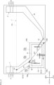
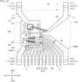
- FIG. 1 is a plan view showing an electronic device according to a first embodiment.
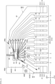
- FIG. 2 is a plan view of FIG. 1 in which the sealing resin is shown by imaginary lines.
- FIG. 3 is an enlarged plan view of a main portion of FIG.
- FIG. 4 is an enlarged plan view of a main portion of FIG.
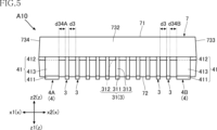
- FIG. 5 is a front view of the electronic device according to the first embodiment.
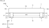
- FIG. 6 is a rear view of the electronic device according to the first embodiment.
- FIG. 7 is a left side view showing the electronic device according to the first embodiment.
- FIG. 8 is a right side view showing the electronic device according to the first embodiment.
- FIG. 9 is a cross-sectional view taken along line IX-IX in FIG.
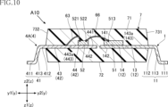
- FIG. 10 is a cross-sectional view taken along line XX in FIG.
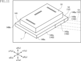
- FIG. 11 is an enlarged perspective view of a main portion showing a first die pad portion and a first electronic component of the electronic device according to the first embodiment.
- FIG. 12 is an enlarged perspective view of a main portion showing a second die pad portion and a second electronic component of the electronic device according to the first embodiment.
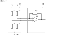
- FIG. 13 is a diagram illustrating a circuit configuration of the first electronic component and the second electronic component of the electronic device according to the first embodiment.
- FIG. 14 is a plan view showing a process for manufacturing the electronic device according to the first embodiment.
- FIG. 15 is a plan view showing an electronic device according to a first modified example of the first embodiment, in which a sealing resin is indicated by imaginary lines.
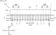
- FIG. 16 is a front view showing an electronic device according to a first modified example of the first embodiment.
- FIG. 16 is a front view showing an electronic device according to a first modified example of the first embodiment.
- FIG. 17 is a rear view showing the electronic device according to the first modified example of the first embodiment.
- FIG. 18 is a plan view showing an electronic device according to a second modified example of the first embodiment, in which the sealing resin is indicated by imaginary lines.
- FIG. 19 is a plan view showing an electronic device according to a third modified example of the first embodiment, in which the sealing resin is indicated by imaginary lines.
- FIG. 20 is a plan view showing an electronic device according to a fourth modified example of the first embodiment, in which the sealing resin is indicated by imaginary lines.
- FIG. 21 is a diagram showing a circuit configuration of a first electronic component and a second electronic component of an electronic device according to a fourth modified example of the first embodiment. In FIG. FIG. FIG.
- FIG. 22 is a plan view showing an electronic device according to another configuration of the fourth modified example of the first embodiment, in which the sealing resin is indicated by imaginary lines.
- FIG. 23 is an enlarged plan view of a main part of an electronic device according to the second embodiment.
- FIG. 24 is an enlarged plan view of a main part of an electronic device according to the second embodiment.
- an object A is formed on an object B
- an object A is formed on (an object B)
- an object A is formed directly on an object B
- an object A is formed on an object B with another object interposed between the object A and the object B” unless otherwise specified.
- an object A is disposed on an object B” and “an object A is disposed on (an object B)” include “an object A is disposed directly on an object B” and “an object A is disposed on (an object B) with another object interposed between the object A and the object B” unless otherwise specified.
- an object A is located on (an object B) includes “an object A is in contact with an object B and is located on (an object B)” and “an object A is located on (an object B) with another object interposed between the object A and the object B".
- an object A overlaps an object B includes “an object A overlaps the entire object B” and “an object A overlaps a part of an object B” unless otherwise specified.
- an object A (its material) contains a certain material C includes “an object A (its material) is made of a certain material C” and “an object A (its material) is mainly composed of a certain material C.”
- a certain surface A faces a certain direction B (one side or the other side) includes, unless otherwise specified, the angle of surface A with respect to direction B is not limited to 90°, and includes the case where surface A is inclined with respect to direction B.
- a certain surface A is perpendicular to a certain surface B includes, unless otherwise specified, the angle of surface A with respect to surface B is not limited to 90°, and includes the case where surface A is inclined with respect to surface B.
- the electronic device A10 includes a first lead 1, a second lead 2, a plurality of third leads 3, a pair of fourth leads 4, a first electronic component 51, a second electronic component 52, a plurality of connecting members 61 to 66, and a sealing resin 7.
- the electronic device A10 includes eleven third leads 3, but the number of third leads 3 is not limited in any way.
- the specific use of the electronic device A10 is not limited in any way, but may be, for example, for detecting the battery voltage of an electric vehicle.
- the electronic device A10 does not detect the battery voltage of an electric vehicle, but may detect other voltages of the electric vehicle, or may detect voltages used in industrial equipment, home appliances, power supplies, etc., other than electric vehicles.
- the electronic device A10 is a surface-mounted semiconductor package, and in this embodiment, it is an SOP (Small Outline Package) type, as shown in FIG. 1 and FIG. 5 to FIG. 8.
- the thickness direction z corresponds to the thickness direction of the electronic device A10 (first electronic component 51).
- Planar view refers to the view in the thickness direction z.
- the first direction y is perpendicular to the thickness direction z.
- the second direction x is perpendicular to the thickness direction z and the first direction y.
- One side of the first direction y is referred to as the y1 side of the first direction y, and the other side of the first direction y is referred to as the y2 side of the first direction y.
- One side of the second direction x is referred to as the x1 side of the second direction x, and the other side of the second direction x is referred to as the x2 side of the second direction x.
- One side of the thickness direction z is referred to as the z1 side of the thickness direction z, and the other side of the thickness direction z is referred to as the z2 side of the thickness direction z.
- the z2 side of the thickness direction z is sometimes referred to as the upper side, and the z1 side of the thickness direction z is sometimes referred to as the lower side.
- Terms such as “top,” “bottom,” “upper,” “lower,” “top surface,” and “bottom surface” indicate the relative positional relationship of each part in the thickness direction z, and do not necessarily define the relationship with the direction of gravity.
- the first lead 1, the second lead 2, the multiple third leads 3, and the pair of fourth leads 4 include metals such as Cu (copper), Ni (nickel), Fe (iron), etc.
- the first lead 1, the second lead 2, the multiple third leads 3, and the pair of fourth leads 4 are formed from the same lead frame (lead frame 9 described below).
- the first lead 1, the second lead 2, the multiple third leads 3, and the pair of fourth leads 4 are formed, for example, by subjecting a metal plate material to a process selected from punching, bending, etching, etc.
- a plating layer made of Ag (silver), Ni, Au (gold), etc. may be provided at appropriate locations on each of the first lead 1, the second lead 2, the multiple third leads 3, and the pair of fourth leads 4, as necessary.
- the first lead 1, the second lead 2, the multiple third leads 3, and the pair of fourth leads 4 are electrically connected to the first electronic component 51 or the second electronic component 52, and form a conductive path in the electronic device A10.
- the first lead 1, the second lead 2, the multiple third leads 3, and the pair of fourth leads 4 are spaced apart from each other.
- the first lead 1, the second lead 2, the multiple third leads 3, and the pair of fourth leads 4 each have a portion covered by the sealing resin 7 and a portion exposed from the sealing resin 7.
- the first lead 1 includes a first outer portion 11 and a first inner portion 12.
- the first outer portion 11 and the first inner portion 12 are connected to each other and formed integrally.
- the boundary between the first outer portion 11 and the first inner portion 12 overlaps with the periphery of the sealing resin 7 in a plan view.
- the first outer part 11 is a part of the first lead 1 that is exposed from the sealing resin 7.
- the first outer part 11 protrudes from the sealing resin 7 to the y2 side in the first direction y.
- the first outer part 11 has a rectangular shape with the first direction y as the longitudinal direction in a plan view.
- the first outer part 11 is bent in a gull-wing shape when viewed in the second direction x.
- the dimension W11 (see FIG. 1) of the first outer part 11 along the second direction x is not limited in any way, but is, for example, 0.1 mm or more and 1.5 mm or less.
- the first outer part 11 includes a first mounting part 111, a first root part 112, and a first relay part 113.
- the first mounting portion 111 is the tip portion of the first outer portion 11.
- the first mounting portion 111 is a portion that is joined to the circuit board when the electronic device A10 is mounted on the circuit board. As shown in Figures 1 and 2, the first mounting portion 111 is located at the end opposite the sealing resin 7 in the first direction y. Therefore, the first mounting portion 111 is located farther from the sealing resin 7 in the first direction y than the first root portion 112 and the first relay portion 113. The first mounting portion 111 is located lower in the thickness direction z than the first root portion 112.
- the first root portion 112 is the root portion of the first outer part 11. As shown in Figures 1 and 2, the first root portion 112 is located at the end of the first outer part 11 that is closer to the sealing resin 7 in the first direction y. Therefore, the first root portion 112 is located closer to the sealing resin 7 in the first direction y than the first mounting part 111 and the first relay part 113. The first root portion 112 is located above the first mounting part 111 in the thickness direction z, and protrudes from the center of the sealing resin 7 in the thickness direction z.
- the first relay portion 113 connects the first mounting portion 111 and the first root portion 112.
- the first relay portion 113 is inclined with respect to the first mounting portion 111 and the first root portion 112 when viewed in the second direction x.
- the first relay portion 113 is inclined with respect to the thickness direction z.
- the first inner portion 12 is a portion of the first lead 1 that is covered with the sealing resin 7.
- the first inner portion 12 extends from the first outer portion 11 inwardly into the sealing resin 7.
- the first inner portion 12 includes a first connecting portion 13 and a first die pad portion 14.
- the first connecting portion 13 extends from the first outer portion 11 inwardly into the sealing resin 7.
- the first connecting portion 13 is connected to the first die pad portion 14.
- the first connecting portion 13 connects the first inner portion 12 and the first die pad portion 14.
- the first die pad portion 14 has the first electronic component 51 mounted thereon and supports the first electronic component 51.
- the first connecting portion 13 is connected to the first die pad portion 14, and the first die pad portion 14 is supported by the first connecting portion 13.
- the first die pad portion 14 is located on the y1 side of the first direction y of the first outer portion 11. Therefore, the first outer portion 11 is disposed on the y2 side of the first direction y with respect to the first die pad portion 14.
- the center of the first die pad portion 14 in the second direction x is located on the x2 side of the second direction x from the center of the first outer portion 11 in the second direction x.
- the center of the first outer portion 11 is located on the x1 side of the second direction x from the center of the first die pad portion 14.
- a part of the first root portion 112 overlaps with the first die pad portion 14 when viewed in the first direction y.
- the entire first root portion 112 may overlap the first die pad portion 14 when viewed in the first direction y.
- the entire first root portion 112 may not overlap the first die pad portion 14.
- the first outer portion 11 may be disposed outward (on the x1 side of the second direction x) from the first die pad portion 14 in the second direction x.
- the first die pad portion 14 has a main surface 141, a back surface 142, and a first side surface 143.
- the main surface 141 and the back surface 142 are spaced apart in the thickness direction z.
- the main surface 141 faces upward in the thickness direction z
- the back surface 142 faces downward in the thickness direction z.
- the first side surface 143 is connected to the main surface 141 and the back surface 142.
- the first side surface 143 faces in the first direction y toward the side where the first outer part 11 is located (the y2 side in the first direction y).
- the first connecting part 13 is connected to the first side surface 143.
- the inclination angle ⁇ 1 of the first connecting part 13 with respect to the first side surface 143 is not limited in any way, but is, for example, 10° or more and 89° or less, and in this embodiment, the inclination angle ⁇ 1 is 45°.
- the first side surface 143 includes a connecting region 143a and a pair of side regions 143b, 143c.
- the connecting region 143a is a region of the first side surface 143 that is connected to the first connecting portion 13.
- the connecting region 143a is in contact with the first connecting portion 13.
- the pair of side regions 143b, 143c are individually arranged on both sides of the connecting region 143a in the second direction x.
- the side region 143b is located on the x1 side of the second direction x with respect to the connecting region 143a, and the side region 143c is located on the x2 side of the second direction x (the same side as the second lead 2) with respect to the connecting region 143a.
- the pair of side regions 143b, 143c are each in contact with the sealing resin 7.
- the connecting region 143a is disposed on the x1 side of the first side surface 143 in the second direction x from the center in the second direction x. Therefore, the dimension in the second direction x of the lateral region 143b is smaller than the dimension in the second direction x of the lateral region 143c.
- the connecting region 143a may be disposed on the x2 side of the first side surface 143 in the second direction x from the center in the second direction x.
- the dimension in the second direction x of the lateral region 143b may be the same as the dimension in the second direction x of the lateral region 143c, or may be larger than the dimension in the second direction x of the lateral region 143c.
- the shape of the first die pad portion 14 in a plan view is rectangular.
- the first die pad portion 14 has a first corner portion 149a, a second corner portion 149b, and two other corner portions 149c and 149d.
- the first corner 149a is located on the y2 side in the first direction y and the x1 side in the second direction x of the four corners of the first die pad portion 14 in a planar view.
- the first corner 149a is closest to the first outer portion 11 of the four corners of the first die pad portion 14.
- the second corner 149b is located on the y1 side in the first direction y and the x2 side in the second direction x of the four corners of the first die pad portion 14 in a planar view.
- the second corner 149b is diagonal to the first corner 149a.
- the second corner 149b is farthest from the first outer portion 11 of the four corners of the first die pad portion 14.
- the corner 149c is located on the y2 side in the first direction y and the x2 side in the second direction x of the four corners of the first die pad portion 14 in a planar view.
- the corner 149d is located on the y1 side in the first direction y and on the x1 side in the second direction x.
- the corner 149d is diagonal to the corner 149c.
- the first corner 149a and the corner 149c are both ends of the first side surface 143 in the second direction x.
- the second lead 2 includes a second outer portion 21 and a second inner portion 22.
- the second outer portion 21 and the second inner portion 22 are connected to each other and formed integrally.
- the boundary between the second outer portion 21 and the second inner portion 22 overlaps with the periphery of the sealing resin 7 in a plan view.
- the second outer part 21 is a portion of the second lead 2 that is exposed from the sealing resin 7.
- the second outer part 21 protrudes from the sealing resin 7 to the y2 side in the first direction y (the same side as the first outer part 11).
- the second outer part 21 has a rectangular shape with the first direction y as its longitudinal direction.
- the plan view shape of the second outer part 21 is congruent with the plan view shape of the first outer part 11, but unlike this configuration, these plan view shapes do not have to be congruent with each other.
- the second outer part 21 is bent in a gull-wing shape when viewed in the second direction x.
- the second outer part 21 overlaps the first outer part 11 when viewed in the second direction x.
- the dimension W21 (see FIG.
- the dimension W21 of the second outer part 21 is not limited in any way and is, for example, 0.1 mm or more and 1.5 mm or less.
- the dimension W21 of the second outer part 21 is the same as the dimension W11 of the first outer part 11, but in some configurations, the dimension W21 and the dimension W11 may be different.
- the second outer part 21 includes a second mounting part 211, a second root part 212, and a second relay part 213.
- the second mounting portion 211 is the tip portion of the second outer portion 21.
- the second mounting portion 211 is a portion that is joined to the circuit board when the electronic device A10 is mounted on the circuit board. As shown in Figures 1 and 2, the second mounting portion 211 is located at the end opposite the sealing resin 7 in the first direction y. Therefore, the second mounting portion 211 is located farther from the sealing resin 7 in the first direction y than the second root portion 212 and the second relay portion 213.
- the second mounting portion 211 is located lower in the thickness direction z than the second root portion 212.
- the second mounting portion 211 is disposed at the same position as the first mounting portion 111 in the thickness direction z.
- the second root portion 212 is the root portion of the second outer part 21. As shown in Figures 1 and 2, the second root portion 212 is located at the end of the second outer part 21 on the sealing resin 7 side in the first direction y. Therefore, the second root portion 212 is located closer to the sealing resin 7 than the second mounting part 211 and the second relay part 213 in the first direction y. The second root portion 212 is located above the second mounting part 211 in the thickness direction z, and protrudes from the center of the sealing resin 7 in the thickness direction z. The second root portion 212 is located at the same position as the first root portion 112 in the thickness direction z.
- the second relay portion 213 connects the second mounting portion 211 and the second root portion 212.
- the second relay portion 213 is inclined with respect to the first mounting portion 111 and the first root portion 112 when viewed in the second direction x.
- the second relay portion 213 is inclined with respect to the thickness direction z.
- the second inner portion 22 is a portion of the second lead 2 that is covered with the sealing resin 7.
- the second inner portion 22 is connected to the second outer portion 21 and extends from the second outer portion 21 inwardly into the sealing resin 7.
- the second inner portion 22 extends from the second outer portion 21 inwardly into the sealing resin 7 so as to approach the first die pad portion 14.
- Each of the multiple third leads 3 includes a third outer portion 31 and a third inner portion 32.
- the electronic device A10 has multiple third outer portions 31 and multiple third inner portions 32.
- the third outer portion 31 and the third inner portion 32 are connected to each other and formed integrally.
- the boundary between the third outer portion 31 and the third inner portion 32 overlaps the periphery of the sealing resin 7 in a plan view.
- the third outer portion 31 and the third inner portion 32 described below are common to each third lead 3 unless otherwise specified.
- the third outer portion 31 is a portion of each third lead 3 that is exposed from the sealing resin 7. Each third outer portion 31 protrudes from the sealing resin 7 to the y1 side of the first direction y (the opposite side to the first outer portion 11 and the second outer portion 21). In a plan view, each third outer portion 31 is in the shape of a strip with the first direction y as its longitudinal direction. The multiple third outer portions 31 are arranged at equal intervals along the second direction x. Each third outer portion 31 is bent in a gull-wing shape when viewed in the second direction x. The multiple third outer portions 31 overlap each other when viewed in the second direction x.
- the dimension W31 (see FIG.
- the third outer portion 31 along the second direction x is not limited in any way, but is, for example, 0.15 mm or more and 0.5 mm or less.
- the dimension W31 of the third outer portion 31 is smaller than the dimension W11 of the first outer portion 11 and the dimension W21 of the second outer portion 21.
- the third outer part 31 includes a third mounting part 311, a third root part 312, and a third relay part 313.
- the electronic device A10 has a plurality of third mounting parts 311, a plurality of third root parts 312, and a plurality of third relay parts 313.
- the third mounting parts 311, the third root parts 312, and the third relay parts 313 described below are common to each third outer part 31 unless otherwise specified.
- the third mounting portion 311 is the tip portion of the third outer portion 31.
- the third mounting portion 311 is a portion that is joined to the circuit board when the electronic device A10 is mounted on the circuit board. As shown in FIG. 1 and FIG. 2, the third mounting portion 311 is located at the end opposite the sealing resin 7 in the first direction y. Therefore, the third mounting portion 311 is located farther from the sealing resin 7 in the first direction y than the third root portion 312 and the third relay portion 313.
- the third mounting portion 311 is located lower in the thickness direction z than the third root portion 312.
- the multiple third mounting portions 311 are arranged at the same position in the thickness direction z.
- the multiple third mounting portions 311 are arranged at equal intervals along the second direction x.
- the third root portion 312 is a root portion of the third outer part 31. As shown in Figures 1 and 2, the third root portion 312 is located at the end of the third outer part 31 on the sealing resin 7 side in the first direction y. Therefore, the third root portion 312 is located closer to the sealing resin 7 than the third mounting part 311 and the third relay part 313 in the first direction y. The third root portion 312 is located above the third mounting part 311 in the thickness direction z, and protrudes from the center of the sealing resin 7 in the thickness direction z. The multiple third root portions 312 are arranged at the same positions as each other in the thickness direction z.
- the third relay portion 313 connects the third mounting portion 311 and the third root portion 312.
- the third relay portion 313 is inclined with respect to the third mounting portion 311 and the third root portion 312 when viewed in the second direction x.
- the third relay portion 313 is inclined with respect to the thickness direction z.
- the third inner portion 32 is a portion of each third lead 3 that is covered with the sealing resin 7.
- the third inner portion 32 is connected to the third outer portion 31 and extends from the third outer portion 31 inwardly into the sealing resin 7.
- the third inner portion 32 extends from the third outer portion 31 inwardly into the sealing resin 7 so as to approach a portion of the fourth lead 4A (second die pad portion 44) described below.
- the pair of fourth leads 4 are arranged on both sides of the multiple third leads 3 in the second direction x.
- one of the pair of fourth leads 4 may be referred to as the "fourth lead 4A” and the other of the pair of fourth leads 4 may be referred to as the "fourth lead 4B".
- the fourth lead 4A is arranged on the x1 side of the second direction x with respect to the multiple third leads 3, and the fourth lead 4B is arranged on the x2 side of the second direction x with respect to the multiple third leads 3.
- the planar shape of the fourth lead 4A is congruent with the planar shape of the first lead 1, but they do not have to be congruent.
- the planar shape of the fourth lead 4B is congruent with the planar shape of the second lead 2, but they do not have to be congruent.
- Each of the pair of fourth leads 4 includes a fourth outer portion 41 and a fourth inner portion 42.
- the fourth outer portion 41 and the fourth inner portion 42 are connected to each other and formed integrally.
- the boundary between the fourth outer portion 41 and the fourth inner portion 42 overlaps the periphery of the sealing resin 7 in a plan view.
- the fourth outer portion 41 and the fourth inner portion 42 described below are common to each fourth lead 4 unless otherwise specified.
- the fourth outer portion 41 is a portion of the fourth lead 4 that is exposed from the sealing resin 7.
- the fourth outer portion 41 protrudes from the sealing resin 7 to the other side in the first direction y.
- the fourth outer portion 41 of the fourth lead 4A is located on the x1 side in the second direction x relative to the multiple third outer portions 31, and the fourth outer portion 41 of the fourth lead 4B is located on the x2 side in the second direction x relative to the multiple third outer portions 31.
- the fourth outer portion 41 is bent in a gull-wing shape when viewed in the second direction x.
- the fourth outer portion 41 overlaps each of the third outer portions 31 when viewed in the second direction x.
- the fourth outer portion 41 is rectangular in plan view with the first direction y as its longitudinal direction.
- the plan view shape of the fourth outer portion 41 is congruent with the plan view shape of the first outer portion 11, but unlike this configuration, these plan view shapes do not have to be congruent with each other.
- the fourth outer portion 41 of the fourth lead 4A overlaps the first outer portion 11 when viewed in the first direction y
- the fourth outer portion 41 of the fourth lead 4B overlaps the second outer portion 21 when viewed in the first direction y.
- the dimension W41 (see FIG. 1 ) of the fourth outer portion 41 along the second direction x is not limited in any way, but is, for example, 0.1 mm or more and 1.5 mm or less.
- the dimension W41 of the fourth outer portion 41 is the same as the dimension W11 of the first outer portion 11 and the dimension W21 of the second outer portion 21, but unlike this configuration, the dimension W41 of the fourth outer portion 41 may be different from the dimension W11 of the first outer portion 11 and the dimension W21 of the second outer portion 21.
- the fourth outer portion 41 includes a fourth mounting portion 411, a fourth root portion 412, and a fourth relay portion 413.
- the fourth mounting portion 411, fourth root portion 412, and fourth relay portion 413 described below are common to the fourth outer portion 41 of each fourth lead 4 unless otherwise specified.
- the fourth mounting portion 411 is the tip portion of the fourth outer portion 41.
- the fourth mounting portion 411 is a portion that is joined to the circuit board when the electronic device A10 is mounted on the circuit board. As shown in Figures 1 and 2, the fourth mounting portion 411 is located at the end opposite the sealing resin 7 in the first direction y. Therefore, the fourth mounting portion 411 is located farther from the sealing resin 7 in the first direction y than the fourth root portion 412 and the fourth relay portion 413.
- the fourth mounting portion 411 is located lower in the thickness direction z than the fourth root portion 412.
- the fourth mounting portion 411 is located at the same position as each third mounting portion 311 in the thickness direction z.
- the fourth mounting portion 411 of the fourth lead 4A is adjacent to the second direction x on the x1 side of the second direction x of the multiple third mounting portions 311.
- the fourth mounting portion 411 of the fourth lead 4B is adjacent to the third mounting portions 311 on the x2 side in the second direction x.
- the fourth mounting portion 411 of the fourth lead 4A overlaps the first mounting portion 111 of the first lead 1 when viewed in the first direction y.
- the fourth mounting portion 411 of the fourth lead 4B overlaps the second mounting portion 211 of the second lead 2 when viewed in the first direction y.
- the fourth root portion 412 is the root portion of the fourth outer part 41. As shown in Figures 1 and 2, the fourth root portion 412 is located at the end of the fourth outer part 41 on the sealing resin 7 side in the first direction y. Therefore, the fourth root portion 412 is located closer to the sealing resin 7 in the first direction y than the fourth mounting part 411 and the fourth relay part 413. The fourth root portion 412 is located above the fourth mounting part 411 in the thickness direction z, and protrudes from the center of the sealing resin 7 in the thickness direction z. The fourth root portion 412 is located at the same position as each third root portion 312 in the thickness direction z.
- the fourth relay portion 413 connects the fourth mounting portion 411 and the fourth root portion 412.
- the fourth relay portion 413 is inclined with respect to the fourth mounting portion 411 and the fourth root portion 412 when viewed in the second direction x.
- the fourth relay portion 413 is inclined with respect to the thickness direction z.
- the fourth inner portion 42 is a portion of the corresponding fourth lead 4 that is covered with the sealing resin 7.
- the fourth inner portion 42 is connected to the fourth outer portion 41 and extends from the fourth outer portion 41 inwardly into the sealing resin 7.
- the fourth inner portion 42 of the fourth lead 4B extends from the fourth outer portion 41 inwardly into the sealing resin 7 so as to approach the second die pad portion 44.
- the fourth inner portion 42 of the fourth lead 4A includes the second connecting portion 43 and the second die pad portion 44.
- the second connecting portion 43 extends from the fourth outer portion 41 inwardly into the sealing resin 7.
- the second connecting portion 43 is connected to the second die pad portion 44.
- the second connecting portion 43 connects the fourth outer portion 41 and the second die pad portion 44.
- the second die pad portion 44 has the second electronic component 52 mounted thereon and supports the second electronic component 52.
- the second connecting portion 43 is connected to the second die pad portion 44, and the second die pad portion 44 is supported by the second connecting portion 43.
- the second die pad portion 44 is spaced apart from the first die pad portion 14.
- the first die pad portion 14 and the second die pad portion 44 are aligned in the first direction y, and the second die pad portion 44 is located on the y1 side of the first direction y from the first die pad portion 14.
- the second die pad portion 44 is located on the y2 side of the first direction y from the fourth outer portion 41. Therefore, the fourth outer portion 41 is disposed on the y1 side of the first direction y from the second die pad portion 44.
- the center in the second direction x of the second die pad portion 44 is located on the x2 side of the second direction x from the center in the second direction x of the fourth outer portion 41 of the fourth lead 4A. Therefore, in the second direction x, the center of the fourth outer portion 41 of the fourth lead 4A is located on the x1 side of the center of the second die pad portion 44 in the second direction x.
- a part of the fourth root portion 412 of the fourth lead 4A overlaps with the second die pad portion 44 when viewed in the first direction y.
- the entire fourth root portion 412 of the fourth lead 4A may overlap with the second die pad portion 44 when viewed in the first direction y.
- the entire fourth root portion 412 of the fourth lead 4A may not overlap with the second die pad portion 44. Therefore, in the fourth lead 4A, the fourth outer portion 41 may be disposed outward (on the x1 side of the second direction x) from the second die pad portion 44 in the second direction x.
- the second die pad portion 44 has a main surface 441, a back surface 442, and a second side surface 443.
- the main surface 441 and the back surface 442 are spaced apart in the thickness direction z.
- the main surface 441 faces upward in the thickness direction z
- the back surface 442 faces downward in the thickness direction z.
- the second side surface 443 is connected to the main surface 441 and the back surface 442.
- the second side surface 443 faces in the first direction y toward the side where the fourth outer part 41 of the fourth lead 4A is located (the y1 side in the first direction y).
- the second connecting part 43 is connected to the second side surface 443.
- the inclination angle ⁇ 1 of the second connecting part 43 with respect to the second side surface 443 is not limited in any way, but is, for example, 10° or more and 89° or less, and in this embodiment, the inclination angle ⁇ 1 is 45°.
- the second side surface 443 includes a connecting region 443a and a pair of side regions 443b, 443c.
- the connecting region 443a is a region of the second side surface 443 that is connected to the second connecting portion 43.
- the connecting region 443a is in contact with the second connecting portion 43.
- the pair of side regions 443b, 443c are individually arranged on both sides of the connecting region 443a in the second direction x.
- the side region 443b is located on the x1 side of the second direction x with respect to the connecting region 443a, and the side region 443c is located on the x2 side of the second direction x with respect to the connecting region 443a (the same side as the fourth lead 4B).
- the pair of side regions 443b, 443c are each in contact with the sealing resin 7.
- the connecting region 443a is disposed on the x1 side of the second direction x from the center in the second direction x of the second side 443. Therefore, the dimension in the second direction x of the lateral region 443b is smaller than the dimension in the second direction x of the lateral region 443c. Unlike this configuration, the connecting region 443a may be disposed on the x2 side of the second direction x from the center in the second direction x of the second side 443. In other words, the dimension in the second direction x of the lateral region 443b may be the same as the dimension in the second direction x of the lateral region 443c, or may be larger than the dimension in the second direction x of the lateral region 443c.
- the shape of the second die pad portion 44 in a plan view is rectangular.
- the second die pad portion 44 has four corners 449a, 449b, 449c, and 449d.
- corner 449a is located on the y1 side in the first direction y and the x1 side in the second direction x among the four corners of the second die pad portion 44 in a planar view. Corner 449a is closest to the fourth outer portion 41 of the fourth lead 4A among the four corners of the second die pad portion 44 in a planar view. Corner 449b is located on the y2 side in the first direction y and the x2 side in the second direction x among the four corners of the second die pad portion 44 in a planar view. Corner 449b is diagonal to corner 449a. Corner 449b is farthest from the fourth outer portion 41 of the fourth lead 4A among the four corners of the second die pad portion 44.
- Corner 449c is located on the y1 side in the first direction y and the x2 side in the second direction x among the four corners of the second die pad portion 44 in a planar view.
- the corner 449d is located on the y2 side in the first direction y and on the x1 side in the second direction x.
- the corner 449d is diagonal to the corner 449c.
- the corners 449a and 449c are both ends of the second side surface 443 in the second direction x.
- the first outer part 11 and the first inner part 12 are adjacent to each other with a distance d12 (see FIG. 6) in the second direction x.
- the multiple third outer parts 31 are arranged with an arrangement distance d3 (see FIG. 5) in the second direction x.
- the distance d12 (see FIG. 6) in the second direction x between the first outer part 11 and the first inner part 12 is larger than the arrangement distance d3 (see FIG. 5) in the second direction x between the third outer parts 31 adjacent to each other in the second direction x.
- the distance d12 is 10 times or more and 20 times or less than the arrangement distance d3.
- the distance d12 is, for example, 5 mm or more and 10 mm or less
- the arrangement distance d3 is, for example, 0.25 mm or more and 5 mm or less.
- the distance d12 is preferably 4 mm or more to prevent a short circuit between the first outer part 11 and the second outer part 21.
- the distance d34A (see FIG. 5) in the second direction x between the fourth outer part 41 of the fourth lead 4A and the third outer part 31 adjacent to the fourth outer part 41, and the distance d34B (see FIG. 5) in the second direction x between the fourth outer part 41 of the fourth lead 4B and the third outer part 31 adjacent to the fourth outer part 41 are the same as the arrangement distance d3.
- the shapes and positional relationships between each of the first die pad portion 14 and the second die pad portion 44 and each of the first inner portion 12, the second inner portion 22, each of the third inner portions 32, and each of the fourth inner portions 42 are not limited to the example shown in the figure, and can be changed as appropriate depending on the specifications of electronic device A10.
- the first electronic component 51 and the second electronic component 52 are elements that perform electrical functions in the electronic device A10.
- the specific functions of the first electronic component 51 and the second electronic component 52 are not limited in any way, but in this embodiment, the first electronic component 51 and the second electronic component 52 have the function of detecting voltage.
- the first electronic component 51 is bonded to the first die pad portion 14 by a bonding material (such as solder or sintered silver) not shown, and is mounted on the first die pad portion 14.
- a bonding material such as solder or sintered silver
- the first electronic component 51 and the connection region 143a of the first die pad portion 14 are arranged along the first direction y in a plan view.
- the first electronic component 51 outputs a first signal corresponding to the potential of the first lead 1 and a second signal corresponding to the potential of the second lead 2 to the second electronic component 52.
- the first electronic component 51 has a plurality of electrodes 511, 512, 513 arranged on the upper surface in the thickness direction z.
- the second electronic component 52 is bonded to the second die pad portion 44 by a bonding material (such as solder or sintered silver) not shown, and is mounted on the second die pad portion 44.
- the second electronic component 52 and the connection region 443a of the second die pad portion 44 are arranged along the first direction y in a plan view.
- the second electronic component 52 receives the first signal and the second signal from the first electronic component 51, and outputs a third signal according to the potential difference between the first lead 1 and the second lead 2.
- the second electronic component 52 outputs a detection signal (third signal) of the voltage applied between the first lead 1 and the second lead 2.
- the second electronic component 52 has a plurality of electrodes 521, 522 arranged on the upper surface in the thickness direction z.
- the first electronic component 51 and the second electronic component 52 have a circuit configuration, for example, as shown in FIG. 13.
- the first electronic component 51 includes a plurality of resistive elements R1 to R4, and the second electronic component 52 includes an operational amplifier OP and a resistive element R5.
- the circuit configuration of the first electronic component 51 and the second electronic component 52 is not limited to the example shown in FIG. 13.
- the two resistive elements R1 and R2 are connected in series with each other.
- the two resistive elements R1 and R2 divide the voltage of terminal T1 (the potential difference between the potential of terminal T1 and the reference potential of ground GND).
- terminal T1 corresponds to multiple electrodes 512.
- the connection point of the two resistive elements R1 and R2 is connected to the non-inverting input terminal of the operational amplifier OP.
- the two resistive elements R3 and R4 are connected in series with each other.
- the two resistive elements R3 and R4 divide the voltage of terminal T2 (the potential difference between the potential of terminal T2 and the reference potential of ground GND).
- terminal T2 corresponds to multiple electrodes 511.
- connection point of the two resistive elements R3 and R4 is connected to the inverting input terminal of the operational amplifier OP.
- electronic device A10 detects the voltage of a battery installed in an electric vehicle, one of terminals T1 and T2 is electrically connected to the high-potential terminal of the battery, and the other is electrically connected to the low-potential terminal.
- the operational amplifier OP receives a first signal (in this embodiment, a signal obtained by dividing the voltage at terminal T1) corresponding to the potential at terminal T1 and a second signal (in this embodiment, a signal obtained by dividing the voltage at terminal T2) corresponding to the potential at terminal T2, and outputs a third signal corresponding to the potential difference between terminals T1 and T2.
- the resistive element R5 is an element (feedback resistor) for determining the amplification gain of the operational amplifier OP, and one end of the resistive element R5 is connected to the inverting input terminal of the operational amplifier OP, and the other end is connected to the output terminal of the operational amplifier OP.
- the second electronic component 52 does not need to include the resistive element R5.
- the multiple connection members 61-66 each electrically connect parts spaced apart from one another.
- the multiple connection members 61-66 are each bonding wires.
- the multiple connection members 61-66 may each be a plate-shaped metal member rather than a bonding wire.
- the multiple connection members 61-66 each contain Au, Al (aluminum), or Cu.
- connection member 61 is joined to the electrode 511 of the first electronic component 51 and the second inner portion 22, and electrically connects the first electronic component 51 and the second lead 2. Therefore, the second outer portion 21 of the second lead 2 is electrically connected to the first electronic component 51 via the second inner portion 22 and the connection member 61.
- connection member 62 is joined to the electrode 512 of the first electronic component 51 and the first connecting portion 13 (first inner portion 12), electrically connecting the first electronic component 51 and the first lead 1. Therefore, the first outer portion 11 of the first lead 1 is electrically connected to the first electronic component 51 via the first connecting portion 13 and the connection member 62.
- each of the multiple connection members 63 is joined to the electrode 521 of the second electronic component 52 and one of the multiple third inner parts 32, electrically connecting the second electronic component 52 to one of the multiple third leads 3. Therefore, each third outer part 31 of the multiple third leads 3 is electrically connected to the second electronic component 52 via the corresponding third inner part 32 and the corresponding connection member 63.
- connection member 64 is joined to the electrode 521 of the second electronic component 52 and the fourth inner portion 42 of the fourth lead 4B, electrically connecting the second electronic component 52 and the fourth lead 4B. Therefore, the fourth outer portion 41 of the fourth lead 4B is electrically connected to the second electronic component 52 via the fourth inner portion 42 of the fourth lead 4B and the connection member 64.
- connection member 65 is joined to the electrode 521 of the second electronic component 52 and the second coupling portion 43 (fourth inner portion 42), electrically connecting the second electronic component 52 and the fourth lead 4A.
- the fourth outer portion 41 of the fourth lead 4A is electrically connected to the second electronic component 52 via the second coupling portion 43 of the fourth lead 4A and the connection member 65.
- the multiple connection members 66 are joined to the electrodes 513 of the first electronic component 51 and the electrodes 522 of the second electronic component 52, electrically connecting the first electronic component 51 and the second electronic component 52.
- the multiple connection members 66 are transmission paths for the first signal and the second signal.
- the sealing resin 7 covers the first lead 1, the second lead 2, the plurality of third leads 3, and a portion of each of the pair of fourth leads 4, the first electronic component 51, the second electronic component 52, and the plurality of connection members 61 to 66.
- the sealing resin 7 includes an insulating material such as an epoxy resin.
- the sealing resin 7 is made of a resin material having a CTI (Comparative Tracking Index) of 600 V or more.
- the method of forming the sealing resin 7 is not limited, but may be, for example, molding.
- the sealing resin 7 has, for example, a rectangular parallelepiped shape.
- the sealing resin 7 has a dimension along the second direction x of, for example, 5 mm or more and 10 mm or less, and a dimension along the first direction y of, for example, 3 mm or more and 13 mm or less.
- the sealing resin 7 has a resin main surface 71, a resin back surface 72, a first resin side surface 731, a second resin side surface 732, and two resin side surfaces 733 and 734.
- the resin main surface 71 and the resin back surface 72 are spaced apart from each other in the thickness direction z.
- the resin main surface 71 faces the z2 side in the thickness direction z
- the resin back surface 72 faces the z1 side in the thickness direction z.
- the resin main surface 71 is the upper surface of the sealing resin 7, and the resin back surface 72 is the lower surface of the sealing resin 7.
- the first resin side surface 731 and the second resin side surface 732 are spaced apart from each other in the first direction y.
- the first resin side surface 731 faces the y2 side of the first direction y
- the second resin side surface 732 faces the y1 side of the first direction y.
- the two resin side surfaces 733, 734 are spaced apart from each other in the second direction x.
- the resin side surface 733 faces the x2 side of the second direction x
- the resin side surface 734 faces the x1 side of the second direction x.
- the first outer portion 11 and the second outer portion 21 each protrude from the first resin side surface 731.
- each third outer portion 31 of the multiple third leads 3 and each fourth outer portion 41 of the pair of fourth leads 4 each protrude from the second resin side surface 732.
- the sum of the distance d11 (see FIG. 3) from the first connection point 191 to the second connection point 192 and the distance d12 (see FIG. 3) from the second connection point 192 to the second corner 149b is shorter than in the case of the following configuration.
- the first connection portion 13 is connected to the first corner 149a (the corner closest to the first outer portion 11) of the four corners of the first die pad portion 14.
- the first connection point 191 is the center of the boundary between the first inner portion 12 and the first outer portion 11 (hereinafter referred to as the "first boundary").
- the first boundary is a line segment along the second direction x as shown in FIG.
- the center of the first boundary is the center of the line segment in the second direction x.
- the second connection point 192 is the center of the boundary (hereinafter referred to as the "second boundary") between the first connection portion 13 and the first die pad portion 14.
- the second boundary is a line segment along the second direction x as shown in FIG. 3, and the center of the second boundary is the center of the line segment in the second direction x.
- the distance d11 is the shortest distance from the first connection point 191 to the second connection point 192 that passes over the first connection portion 13
- the distance d12 is the shortest distance from the second connection point 192 to the second corner portion 149b that passes over the first die pad portion 14.
- the sum of the distance d21 (see FIG. 4) from the connection point 491 to the connection point 492 and the distance d22 (see FIG. 4) from the connection point 492 to the corner 449b is shorter than in the case of the following configuration.
- the second connection portion 43 is connected to the corner 449a (the corner closest to the fourth outer portion 41 of the fourth lead 4A) among the four corners of the second die pad portion 44.
- the connection point 491 is the center of the boundary (hereinafter referred to as the "third boundary") between the fourth inner portion 42 of the fourth lead 4A and the fourth outer portion 41 of the fourth lead 4A.
- the third boundary is a line segment along the second direction x as shown in FIG. 4, and the center of the third boundary is the center of the line segment in the second direction x.
- the connection point 492 is the center of the boundary (hereinafter referred to as the "fourth boundary") between the second connection portion 43 and the second die pad portion 44.
- the fourth boundary is a line segment along the second direction x as shown in FIG. 4, and the center of the fourth boundary is the center of the line segment in the second direction x.
- the distance d21 is the shortest distance from the connection point 491 to the connection point 492 that passes through the second connection portion 43
- the distance d22 is the shortest distance from the connection point 492 to the corner portion 449b that passes through the second die pad portion 44.
- FIG. 14 shows a process in the manufacture of the electronic device A10.
- FIG. 14 shows the state before the sealing resin 7 is formed.
- the first lead 1, the second lead 2, the multiple third leads 3, and the pair of fourth leads 4 are connected to each other by a tie bar 91 and are included in one lead frame 9.
- this tie bar 91 is connected to the first outer part 11 of the first lead 1, the second outer part 21 of the second lead 2, each third outer part 31 of the multiple third leads 3, and each fourth outer part 41 of the pair of fourth leads 4.
- the first inner part 12 is supported by the tie bar 91 at the connection point C1 shown in FIG. 14.
- the fourth inner part 42 of the fourth lead 4A is supported by the tie bar 91 at the connection point C2 shown in FIG. 14.
- the first electronic component 51 and the second electronic component 52 are mounted (joined) on the lead frame 9 shown in FIG. 14, and the connection members 61-66 are formed (wire bonded) and then the sealing resin 7 is formed, for example, by molding.
- the first lead 1, the second lead 2, the multiple third leads 3, and the pair of fourth leads 4 are each cut off from the tie bar 91, and the first outer part 11, the second outer part 21, the third outer parts 31, and the fourth outer parts 41 are each bent to manufacture electronic device A10.
- the center of the first outer part 11 is disposed on the x1 side of the center of the first die pad part 14 in the second direction x.
- the first outer part 11 is shifted from the first die pad part 14 in both directions in the second direction x.
- the connection position of the first connecting part 13 to the first die pad part 14 will be farther away from the center of the first die pad part 14.
- the first side surface 143 includes a connecting region 143a connected to the first connecting part 13, and a pair of side regions 143b, 143c disposed on both sides of the connecting region 143a in the second direction x.
- the connection position of the first connecting portion 13 to the first die pad portion 14 is closer to the center in the second direction x than to the edge of the first die pad portion 14 in the second direction x, so the connection position is closer to the center of the first die pad portion 14. Therefore, in the electronic device A10, the weight of the first die pad portion 14 can reduce the stress applied to the connection portion between the first connecting portion 13 and the first die pad portion 14. In other words, the electronic device A10 can reduce deformation of the first lead 1, i.e., deformation of the lead frame.
- the second side surface 443 includes a connection region 443a connected to the second connecting portion 43 and a pair of side regions 443b, 443c arranged on either side of the connection region 443a in the second direction x, so that the connection position of the second connecting portion 43 to the second die pad portion 44 approaches the center of the second die pad portion 44.
- the weight of the second die pad portion 44 can reduce the stress applied to the connection portion between the second connecting portion 43 and the second die pad portion 44, so that deformation of the fourth lead 4A, i.e., deformation of the lead frame, can be reduced.
- the sum of the distance d11 and the distance d12 is smaller than in a configuration in which the first connecting portion 13 is connected to the first corner 149a (the corner closest to the first outer portion 11) of the four corners of the first die pad portion 14.
- This configuration can reduce deformation of the first lead 1.
- the first inner portion 12 is supported by the tie bar 91 at the connection point C1. In this configuration, a bending moment occurs at the connection point C1 due to an external force applied to the first die pad portion 14.
- the external force is applied to the first die pad portion 14, for example, during the manufacturing process of the electronic device A10, when the lead frame 9 is transported, when the first electronic component 51 is joined to the first die pad portion 14, and when the connection members 61 and 62 are bonded to the first electronic component 51.
- the sum of distance d11 and distance d12 is smaller than in a configuration in which first connecting portion 13 is connected to first corner 149a (the corner closest to first outer portion 11) of the four corners of first die pad portion 14. In other words, electronic device A10 can reduce the bending moment acting on connection point C1, thereby reducing deformation of first lead 1.
- the electronic device A10 can reduce the bending moment applied to the connection point C2, thereby reducing deformation of the fourth lead 4A.
- the side of the first die pad portion 14 is in contact with the sealing resin 7, except for the connecting region 143a.
- the side of the first die pad portion 14 is the surface of the first die pad portion 14 that is connected to the main surface 141 and the back surface 142 and is sandwiched between them, and a part of it is the first side surface 143.
- the inclination angle ⁇ 1 of the first connecting portion 13 relative to the first side surface 143 is 10° or more and 89° or less.
- the first connecting portion 13 is connected to the first side surface 143 at an acute angle. This reduces the strength at the second boundary, increasing the possibility of deformation at the second boundary.
- the second boundary approaches the first corner portion 149a. This increases the sum of the distance d11 and the distance d12, increasing the possibility of deformation at the connection point C1.
- the electronic device A10 can appropriately reduce deformation at the second boundary and deformation at the connection point C1, which is preferable for reducing deformation of the first lead 1.
- the inclination angle ⁇ 1 to 45°, deformation at the second boundary and deformation at the connection point C1 are suppressed in a balanced manner, which is even more preferable in reducing deformation of the first lead 1.
- the inclination angle ⁇ 1 of the second connecting portion 43 relative to the second side surface 443 is greater than or equal to 10° and less than or equal to 89°, which is preferable in terms of reducing deformation of the fourth lead 4A because it is possible to appropriately reduce deformation at the fourth boundary and at the connection point C2.
- the inclination angle ⁇ 1 to 45°, deformation at the fourth boundary and at the connection point C2 are reduced in a balanced manner, which is even more preferable in terms of reducing deformation of the fourth lead 4A.
- connecting region 143a is disposed on the x1 side in the second direction x (i.e., the side where the center in the second direction x of first outer part 11 is located and where first corner part 149a is located) of first side surface 143 from the center in the second direction x.
- This configuration is preferable for setting inclination angle ⁇ 1 of first connecting part 13 with respect to first side surface 143 to be 30° or more and 45° or less.
- connection region 443a is disposed on the second side surface 443, on the x1 side in the second direction x from the center in the second direction x (i.e., the side where the center in the second direction x of the fourth outer portion 41 of the fourth lead 4A is located, and where the corner portion 449a is located).
- This configuration is preferable for making the inclination angle ⁇ 1 of the second connection portion 43 with respect to the second side surface 443 greater than or equal to 30° and less than or equal to 45°.
- this is preferable for ensuring an area in which multiple third leads 3 can be disposed between a pair of fourth leads 4.
- the first outer part 11 and the second outer part 21 are adjacent to each other in the second direction x with a distance d12 therebetween, and the multiple third outer parts 31 are arranged with a spacing d3 therebetween in the second direction x.
- the spacing d12 is greater than the spacing d3.
- the electronic device A10 it is possible to reduce discharge between the first outer part 11 and the second outer part 21 while miniaturizing the device.
- the electronic device A10 has a package structure that is favorable for reducing discharge between the first outer part 11 and the second outer part 21.
- FIGS. 15 to 17 show an electronic device A11 according to a first modified example of the first embodiment.
- the electronic device A11 differs from the electronic device A10 in the following respects. That is, the configurations of the first lead 1, the second lead 2, and the pair of fourth leads 4 are different.
- the first lead 1 of the electronic device A11 includes two first outer parts 11 that are separated from each other. Unlike the illustrated example, the number of the first outer parts 11 may be three or more.
- Each of the two first outer parts 11 includes a first mounting part 111, a first root part 112, and a first relay part 113.
- the two first outer parts 11 are adjacent to each other in the second direction x with a distance d1 therebetween.
- the distance d1 is, for example, the same as the arrangement distance d3, but these may be different. Due to this configuration, the first inner part 12 of the first lead 1 has an end part that is connected to each first outer part 11 and is bifurcated into two.
- the two first outer parts 11 are electrically connected to each other by the first inner part 12, and therefore have the same potential. Furthermore, since the first lead 1 includes two first outer parts 11, the first lead 1 includes two of the first boundaries. In this example, the first connection point 191 may be the midpoint between the two first boundaries, as shown in FIG. 15.
- the second lead 2 of the electronic device A11 includes two second outer parts 21 that are separated from each other. Unlike the illustrated example, the number of second outer parts 21 may be three or more.
- Each of the two second outer parts 21 includes a second mounting part 211, a second root part 212, and a second relay part 213.
- the two second outer parts 21 are adjacent to each other in the second direction x with a distance d2 therebetween.
- the distance d2 is, for example, the same as the arrangement distance d3, but these may be different.
- the second inner part 22 of the second lead 2 has a bifurcated end on the side connected to each second outer part 21. Therefore, the two second outer parts 21 are electrically connected to each other by the second inner parts 22 and are at the same potential.
- each fourth lead 4 of the electronic device A11 includes two fourth outer parts 41 that are separated from each other. Unlike the illustrated example, the number of fourth outer parts 41 may be three or more.
- the two fourth outer parts 41 each include a fourth mounting part 411, a fourth root part 412, and a fourth relay part 413. As shown in FIG. 16, the two fourth outer parts 41 are adjacent to each other in the second direction x with a distance d41 therebetween.
- the distance d41 is, for example, the same as the above-mentioned arrangement distance d3, but these may be different. Due to this configuration, the fourth inner part 42 of each fourth lead 4 has an end part that is connected to each fourth outer part 41 and is bifurcated into two.
- each fourth lead 4 the two fourth outer parts 41 are electrically connected to each other by the fourth inner part 42, and therefore have the same potential.
- the fourth lead 4A since the fourth lead 4A includes two fourth outer parts 41, the fourth lead 4A includes two of the above-mentioned third boundaries.
- the connection point 491 may be the midpoint between the two third boundaries, as shown in FIG. 15.
- electronic device A11 can reduce deformation of the first lead 1 and the fourth lead 4A, i.e., deformation of the lead frame.
- electronic device A11 has a common configuration with electronic device A10, and thus achieves the same effects.
- the first lead 1, the second lead 2, and the pair of fourth leads 4 are each described as being bifurcated inside the sealing resin 7, but at least one of these does not have to be bifurcated, as in the electronic device A10.
- FIG. 18 shows an electronic device A12 according to a second modified example of the first embodiment.
- the electronic device A12 differs from the electronic device A10 in the following respect. That is, a plurality of third leads 3 are further disposed between the first lead 1 and the second lead 2.
- the multiple third leads 3 arranged between the first lead 1 and the second lead 2 protrude from the first resin side surface 731.
- the third outer parts 31 of the multiple third leads 3 are arranged between the first outer part 11 and the second outer part 21 in the second direction x.
- the first outer part 11 is arranged on the x1 side in the second direction x from the third outer parts 31 of the multiple third leads 3.
- the first outer part 11 is located furthest from the x1 side in the second direction x among the first outer part 11, the second outer part 21 and the multiple third outer parts 31 protruding from the first resin side surface 731.
- Such a configuration can be adopted, for example, when each of the first electronic component 51 and the second electronic component 52 is an IC (Integrated Circuit).
- electronic device A12 like electronic device A10, deformation of the first lead 1 and deformation of the fourth lead 4A, i.e., deformation of the lead frame, can be reduced.
- electronic device A12 has a common configuration with electronic devices A10 and A11, and thus achieves the same effects.
- FIG. 19 shows an electronic device A13 according to a third modified example of the first embodiment.
- the electronic device A13 differs from the electronic device A10 in the following respect. That is, the electronic device A13 does not include any of the multiple third leads 3.
- electronic device A13 like electronic device A10, deformation of the first lead 1 and deformation of the fourth lead 4A, i.e., deformation of the lead frame, can be reduced.
- electronic device A13 has a common configuration with each of electronic devices A10 to A12, and thus achieves the same effects.
- the 20 and 21 show an electronic device A14 according to a fourth modified example of the first embodiment.
- the electronic device A14 differs from the electronic device A10 in the following respect. That is, the functions of the first electronic component 51 and the second electronic component 52 are different.
- the first electronic component 51 and the second electronic component 52 have a power conversion function rather than a voltage detection function.
- the first electronic component 51 and the second electronic component 52 are each switching elements.
- the first electronic component 51 and the second electronic component 52 are each an IGBT (Insulated Gate Bipolar Transistor), but they may be other transistors such as MOSFETs (Metal-Oxide-Semiconductor Field Effect Transistors) or bipolar transistors instead of IGBTs.
- the first electronic component 51 has three electrodes 511, 512, and 513.
- the electrode 511 is a gate
- the electrode 512 is an emitter
- the electrode 513 is a collector.
- the first electronic component 51 is configured, for example, in a vertical structure, with two electrodes 511 and 512 arranged on the upper surface (surface facing upward in the thickness direction z) and an electrode 513 arranged on the lower surface (surface facing downward in the thickness direction z).
- the first electronic component 51 is joined to the first die pad portion 14 by a conductive bonding material (such as solder) not shown.
- the electrode 513 provided on the lower surface of the first electronic component 51 is electrically connected to the first die pad portion 14 via the conductive bonding material.
- the second electronic component 52 has three electrodes 521, 522, and 523.
- the electrode 521 is a gate
- the electrode 522 is an emitter
- the electrode 523 is a collector.
- the second electronic component 52 is configured, for example, in a vertical structure, with two electrodes 521 and 522 arranged on the upper surface (surface facing upward in the thickness direction z) and an electrode 523 arranged on the lower surface (surface facing downward in the thickness direction z).
- the second electronic component 52 is joined to the second die pad portion 44 by a conductive bonding material (for example, solder, etc.) not shown.
- the electrode 523 provided on the lower surface of the second electronic component 52 is conductive to the second die pad portion 44 (fourth lead 4A) via the conductive bonding material.
- the first electronic component 51 and the second electronic component 52 may each have a horizontal structure rather than a vertical structure.
- the electrode 513 is disposed on the upper surface of the first electronic component 51
- the electrode 523 is disposed on the upper surface of the second electronic component 52.
- the electrode 513 and the first inner portion 12 are electrically connected by a bonding wire or a plate-shaped metal member
- the electrode 523 and the fourth inner portion 42 of the fourth lead 4A are electrically connected by a bonding wire or a plate-shaped metal member.
- connection members 61 to 66 In electronic device A14, in addition to the multiple connection members 61 to 66, multiple connection members 67 are provided.
- the multiple connection members 67 are bonding wires, just like each of the connection members 61 to 66.
- each of the connection members 61 to 67 is joined as follows.
- the multiple connection members 61 are each bonded to the electrode 512 and the second die pad portion 44, electrically connecting them.
- the second die pad portion 44 (the fourth inner portion 42 of the fourth lead 4A) is electrically connected to the electrode 512 via the multiple connection members 61.
- the multiple connection members 64 are each bonded to the electrode 522 and the second inner portion 22 of the second lead 2, electrically connecting them.
- the second lead 2 is electrically connected to the electrode 522 via the multiple connection members 64.
- the multiple connection members 67 are bonded to the second die pad portion 44 and the fourth inner portion 42 of the fourth lead 4B, electrically connecting them.
- the fourth lead 4B is electrically connected to the fourth lead 4A via the multiple connection members 67.
- the fourth lead 4B is electrically connected to the electrode 523.
- connection member 62 is joined to the electrode 511 and the third inner portion 32 of one of the multiple third leads 3, electrically connecting them.
- the third outer portion 31 of the third lead 3 to which the connection member 62 is joined is a signal input terminal that inputs a drive signal for the first electronic component 51.
- the connection member 63 is joined to the electrode 512 and the third inner portion 32 of one of the multiple third leads 3, electrically connecting them.
- the third outer portion 31 of the third lead 3 to which the connection member 63 is joined is a detection terminal for detecting the current (emitter current in the electronic device A14) flowing through the first electronic component 51.
- connection member 65 is joined to the electrode 521 and the third inner portion 32 of one of the multiple third leads 3, electrically connecting them.
- the third outer portion 31 of the third lead 3 to which the connection member 65 is joined is a signal input terminal that inputs a drive signal for the second electronic component 52.
- the connection member 66 is joined to the electrode 522 and the third inner portion 32 of one of the multiple third leads 3, electrically connecting them.
- the third outer portion 31 of the third lead 3 to which the connection member 66 is connected is a detection terminal for detecting the current (emitter current in the electronic device A14) flowing through the second electronic component 52.
- a power supply voltage (e.g., DC voltage) is applied to the first outer part 11 (first lead 1) and the second outer part 21 (second lead 2), and the power supply voltage is converted to a predetermined voltage (e.g., AC voltage) by the switching operations of the first electronic component 51 and the second electronic component 52.
- a predetermined voltage e.g., AC voltage
- the signal input terminal and detection terminal for the first electronic component 51 may be any of the multiple third leads 3 arranged between a pair of fourth leads 4. In this case, it is not necessary to provide either of the two third leads 3 between the first lead 1 and the second lead 2.
- electronic device A14 can reduce deformation of the first lead 1 and the fourth lead 4A, i.e., deformation of the lead frame.
- electronic device A14 has a common configuration with each of electronic devices A10 to A13, and thus achieves the same effects.
- both the first electronic component 51 and the second electronic component 52 are switching elements.
- the second electronic component 52 may be a control IC that controls the driving of the first electronic component 51, rather than a switching element.
- FIG. 22 shows an electronic device according to such a modified example of the fourth embodiment.
- the second electronic component 52 outputs a drive signal to the first electronic component 51 via a connection member 66.
- the second electronic component 52 detects the current flowing through the first electronic component 51 via a connection member 67.
- the multiple connection members 61 are joined to the electrode 512 and the second inner portion 22.
- the electronic device configured in this manner also achieves the same effects as the electronic device A14.
- the function of the first electronic component 51 and the second electronic component 52 is not limited to a voltage detection function.
- the first electronic component 51 and the second electronic component 52 include semiconductor elements made of semiconductor materials.
- the electronic device of the present disclosure includes a semiconductor device including semiconductor elements as the first electronic component 51 and the second electronic component 52.
- the arrangement and number of the multiple third leads 3 and the arrangement and number of the multiple connection members 61 to 67 are not limited to the configurations shown in the figures, and can be changed as appropriate according to the specifications of the electronic device.
- FIGS. 23 and 24 show electronic device A20 according to the second embodiment.
- Electronic device A20 differs from electronic device A10 in the following respects. First, in electronic device A20, first connection point 191, second connection point 192, and second corner portion 149b are aligned in a straight line. Second, in electronic device A20, connection point 491, connection point 492, and corner portion 449b are aligned in a straight line.
- first side 143 includes connecting region 143a and a pair of side regions 143b, 143c. Therefore, like electronic device A10, electronic device A20 can reduce deformation of first lead 1, i.e., deformation of the lead frame.
- second side 443 includes connecting region 443a and a pair of side regions 443b, 443c. Therefore, like electronic device A10, electronic device A20 can reduce deformation of fourth lead 4A, i.e., deformation of the lead frame.
- electronic device A20 has a common configuration with electronic device A10, and thus achieves the same effects.
- first connection point 191, second connection point 192, and second corner 149b are aligned in a straight line. This configuration can minimize the sum of distance d11 between first connection point 191 and second connection point 192, and distance d12 between second connection point 192 and second corner 149b. Therefore, electronic device A20 can reduce deformation of first lead 1 more than electronic device A10.
- connection point 491, connection point 492, and corner 449b are aligned in a straight line. This configuration makes it possible to minimize the sum of distance d21 between connection point 491 and connection point 492 and distance d22 between connection point 492 and corner 449b. Therefore, electronic device A20 can reduce deformation of fourth lead 4A more than electronic device A10.
- the electronic device of the present disclosure is not limited to one including both the first electronic component 51 and the second electronic component 52, but may be configured to include only one of the first electronic component 51 and the second electronic component 52.
- a configuration including the first electronic component 51 and not the second electronic component 52 may not include either the multiple third leads 3 or the pair of fourth leads 4.
- a configuration including the second electronic component 52 and not the first electronic component 51 may not include either the first lead 1 or the second lead 2.
- the electronic device according to the present disclosure is not limited to the above-described embodiment.
- the specific configuration of each part of the electronic device according to the present disclosure can be freely designed.
- the electronic device according to the present disclosure includes the following embodiments.
- Appendix 1 Electronic components, A sealing resin for covering the electronic components; a first lead including a first inner portion covered with the sealing resin and a first outer portion exposed from the sealing resin; Equipped with the first inner portion includes a first die pad portion on which the electronic component is mounted, and a first connecting portion connecting the first outer portion and the first die pad portion, the first outer portion is disposed on one side in a first direction perpendicular to a thickness direction of the electronic component with respect to the first die pad portion, the first die pad portion has a first side surface facing a side where the first outer portion is located in the first direction; The first connecting portion is connected to the first side surface, a center of the first outer portion is disposed on one side of the second direction perpendicular to the first direction with respect to a center of the first die
- the first die pad portion is rectangular when viewed in the thickness direction, 2.
- Appendix 3. a center of a boundary between the first inner portion and the first outer portion is defined as a first connecting point; a center of a boundary between the first connection portion and the first die pad portion is defined as a second connection point; 3.
- the electronic device of claim 2, wherein the first connecting portion, the second connecting point, and the second corner portion are aligned in a straight line when viewed in the thickness direction.
- the electronic device according to claim 1 or 2 wherein the connecting region is disposed on one side of the first side in the second direction from a center in the second direction. Appendix 5. 5. The electronic device according to claim 1, wherein the connecting region and the electronic component are arranged along the first direction when viewed in the thickness direction. Appendix 6. 6. The electronic device according to claim 1, wherein the first connecting portion is inclined with respect to the first side surface when viewed in the thickness direction. Appendix 7. 7. The electronic device of claim 6, wherein an inclination angle of the first connecting portion with respect to the first side surface is greater than or equal to 10° and less than or equal to 89°. Appendix 8.
- a second lead spaced apart from the first lead; a conductive member joined to the second lead and the electronic component, the second lead includes a second inner portion covered with the sealing resin and a second outer portion exposed from the sealing resin; 8.
- the conductive member is covered with the sealing resin and joined to the second inner portion.
- Appendix 9. the sealing resin has a first resin side surface facing the one side of the first direction, 9.
- Appendix 10. a plurality of third leads, each of the third leads being spaced apart from the first and second leads; 10.
- each of the plurality of third leads includes a third inner portion covered with the sealing resin and a third outer portion exposed from the sealing resin.
- Appendix 11. each of the third leads protrudes from the first resin side surface;
- the electronic device of claim 10 wherein the first outer portion is positioned on one side of the second direction relative to the second outer portion and the third outer portions of each of the plurality of third leads.
- Appendix 12. the sealing resin has a second resin side surface facing an opposite side to the first resin side surface in the first direction, 11.
- each of the third leads protrudes from the second resin side surface when viewed in the thickness direction. Appendix 13.
- the first outer portion and the second outer portion are adjacent to each other with a first interval therebetween in the second direction,
- the third outer portions of the plurality of third leads are arranged at second intervals in the second direction, 13.
- Appendix 14 a pair of fourth leads each including a fourth inner portion covered with the sealing resin and a fourth outer portion exposed from the sealing resin; each of the pair of fourth leads is spaced apart from the first lead, the second lead, and the plurality of third leads, and protrudes from the second resin side surface when viewed in the thickness direction;
- the electronic device of claim 13 wherein the fourth outer portion of each of the pair of fourth leads is disposed on either side of the third outer portion of the plurality of third leads in the first direction.
- the electronic component is a first electronic component, and a second electronic component is further provided,
- the pair of fourth leads are spaced apart from each other,
- the second die pad portion has a second side surface facing a side where the one of the pair of fourth leads is located in the first direction, The second connecting portion is connected to the second side surface, 16.
Landscapes
- Structures Or Materials For Encapsulating Or Coating Semiconductor Devices Or Solid State Devices (AREA)
Priority Applications (1)
| Application Number | Priority Date | Filing Date | Title |
|---|---|---|---|
| JP2025531457A JPWO2025009349A1 (https=) | 2023-07-04 | 2024-06-13 |
Applications Claiming Priority (2)
| Application Number | Priority Date | Filing Date | Title |
|---|---|---|---|
| JP2023-110016 | 2023-07-04 | ||
| JP2023110016 | 2023-07-04 |
Related Child Applications (1)
| Application Number | Title | Priority Date | Filing Date |
|---|---|---|---|
| US19/434,178 Continuation US20260130297A1 (en) | 2023-07-04 | 2025-12-29 | Electronic device |
Publications (1)
| Publication Number | Publication Date |
|---|---|
| WO2025009349A1 true WO2025009349A1 (ja) | 2025-01-09 |
Family
ID=94171689
Family Applications (1)
| Application Number | Title | Priority Date | Filing Date |
|---|---|---|---|
| PCT/JP2024/021456 Ceased WO2025009349A1 (ja) | 2023-07-04 | 2024-06-13 | 電子装置 |
Country Status (2)
| Country | Link |
|---|---|
| JP (1) | JPWO2025009349A1 (https=) |
| WO (1) | WO2025009349A1 (https=) |
Citations (6)
| Publication number | Priority date | Publication date | Assignee | Title |
|---|---|---|---|---|
| JPS5054058U (https=) * | 1973-09-17 | 1975-05-23 | ||
| JPH10340988A (ja) * | 1997-06-09 | 1998-12-22 | Nec Corp | リードフレームとその製造方法 |
| JP2000150759A (ja) * | 1998-11-04 | 2000-05-30 | Denso Corp | 樹脂封止型半導体装置 |
| JP2017135336A (ja) * | 2016-01-29 | 2017-08-03 | ルネサスエレクトロニクス株式会社 | 半導体装置の製造方法 |
| JP2017174885A (ja) * | 2016-03-22 | 2017-09-28 | ルネサスエレクトロニクス株式会社 | 半導体装置 |
| WO2023112735A1 (ja) * | 2021-12-17 | 2023-06-22 | ローム株式会社 | 電子装置 |
-
2024
- 2024-06-13 WO PCT/JP2024/021456 patent/WO2025009349A1/ja not_active Ceased
- 2024-06-13 JP JP2025531457A patent/JPWO2025009349A1/ja active Pending
Patent Citations (6)
| Publication number | Priority date | Publication date | Assignee | Title |
|---|---|---|---|---|
| JPS5054058U (https=) * | 1973-09-17 | 1975-05-23 | ||
| JPH10340988A (ja) * | 1997-06-09 | 1998-12-22 | Nec Corp | リードフレームとその製造方法 |
| JP2000150759A (ja) * | 1998-11-04 | 2000-05-30 | Denso Corp | 樹脂封止型半導体装置 |
| JP2017135336A (ja) * | 2016-01-29 | 2017-08-03 | ルネサスエレクトロニクス株式会社 | 半導体装置の製造方法 |
| JP2017174885A (ja) * | 2016-03-22 | 2017-09-28 | ルネサスエレクトロニクス株式会社 | 半導体装置 |
| WO2023112735A1 (ja) * | 2021-12-17 | 2023-06-22 | ローム株式会社 | 電子装置 |
Also Published As
| Publication number | Publication date |
|---|---|
| JPWO2025009349A1 (https=) | 2025-01-09 |
Similar Documents
| Publication | Publication Date | Title |
|---|---|---|
| JP5550553B2 (ja) | 電力用半導体モジュール | |
| US7615854B2 (en) | Semiconductor package that includes stacked semiconductor die | |
| US10229884B2 (en) | Semiconductor device | |
| CN113380774B (zh) | 功率半导体模块 | |
| JP4660214B2 (ja) | 電力用半導体装置 | |
| US20240332138A1 (en) | Electronic device | |
| US20250006621A1 (en) | Electronic device | |
| WO2025009349A1 (ja) | 電子装置 | |
| JP2019140175A (ja) | 半導体モジュール | |
| US10490489B2 (en) | Conductive clip connection arrangements for semiconductor packages | |
| US20260130297A1 (en) | Electronic device | |
| JP4695041B2 (ja) | 半導体装置 | |
| US20240332137A1 (en) | Electronic device | |
| WO2024095795A1 (ja) | 電子装置 | |
| WO2022220013A1 (ja) | 半導体装置 | |
| US20250293126A1 (en) | Electronic device | |
| CN118525371A (zh) | 电子装置 | |
| US20260096451A1 (en) | Electronic device | |
| US20250321248A1 (en) | Electronic Component Having a Shunt Between a First Terminal and a Second Terminal | |
| US20240178194A1 (en) | Semiconductor module | |
| US20240030109A1 (en) | Semiconductor device | |
| US20240234267A1 (en) | Semiconductor device | |
| US20250079272A1 (en) | Semiconductor device and manufacturing method | |
| US20250279339A1 (en) | Semiconductor device and external connection main terminal | |
| WO2022168606A1 (ja) | 半導体装置 |
Legal Events
| Date | Code | Title | Description |
|---|---|---|---|
| 121 | Ep: the epo has been informed by wipo that ep was designated in this application |
Ref document number: 24835866 Country of ref document: EP Kind code of ref document: A1 |
|
| ENP | Entry into the national phase |
Ref document number: 2025531457 Country of ref document: JP Kind code of ref document: A |
|
| WWE | Wipo information: entry into national phase |
Ref document number: 2025531457 Country of ref document: JP |
|
| NENP | Non-entry into the national phase |
Ref country code: DE |