WO2025009277A1 - 半導体装置 - Google Patents
半導体装置 Download PDFInfo
- Publication number
- WO2025009277A1 WO2025009277A1 PCT/JP2024/018628 JP2024018628W WO2025009277A1 WO 2025009277 A1 WO2025009277 A1 WO 2025009277A1 JP 2024018628 W JP2024018628 W JP 2024018628W WO 2025009277 A1 WO2025009277 A1 WO 2025009277A1
- Authority
- WO
- WIPO (PCT)
- Prior art keywords
- trench
- contact
- region
- sub
- semiconductor device
- Prior art date
- Legal status (The legal status is an assumption and is not a legal conclusion. Google has not performed a legal analysis and makes no representation as to the accuracy of the status listed.)
- Ceased
Links
Images


Classifications
-
- H—ELECTRICITY
- H10—SEMICONDUCTOR DEVICES; ELECTRIC SOLID-STATE DEVICES NOT OTHERWISE PROVIDED FOR
- H10D—INORGANIC ELECTRIC SEMICONDUCTOR DEVICES
- H10D12/00—Bipolar devices controlled by the field effect, e.g. insulated-gate bipolar transistors [IGBT]
- H10D12/01—Manufacture or treatment
- H10D12/031—Manufacture or treatment of IGBTs
- H10D12/032—Manufacture or treatment of IGBTs of vertical IGBTs
- H10D12/035—Etching a recess in the emitter region
-
- H—ELECTRICITY
- H10—SEMICONDUCTOR DEVICES; ELECTRIC SOLID-STATE DEVICES NOT OTHERWISE PROVIDED FOR
- H10D—INORGANIC ELECTRIC SEMICONDUCTOR DEVICES
- H10D12/00—Bipolar devices controlled by the field effect, e.g. insulated-gate bipolar transistors [IGBT]
- H10D12/01—Manufacture or treatment
- H10D12/031—Manufacture or treatment of IGBTs
- H10D12/032—Manufacture or treatment of IGBTs of vertical IGBTs
- H10D12/038—Manufacture or treatment of IGBTs of vertical IGBTs having a recessed gate, e.g. trench-gate IGBTs
-
- H—ELECTRICITY
- H10—SEMICONDUCTOR DEVICES; ELECTRIC SOLID-STATE DEVICES NOT OTHERWISE PROVIDED FOR
- H10D—INORGANIC ELECTRIC SEMICONDUCTOR DEVICES
- H10D12/00—Bipolar devices controlled by the field effect, e.g. insulated-gate bipolar transistors [IGBT]
- H10D12/411—Insulated-gate bipolar transistors [IGBT]
- H10D12/415—Insulated-gate bipolar transistors [IGBT] having edge termination structures
-
- H—ELECTRICITY
- H10—SEMICONDUCTOR DEVICES; ELECTRIC SOLID-STATE DEVICES NOT OTHERWISE PROVIDED FOR
- H10D—INORGANIC ELECTRIC SEMICONDUCTOR DEVICES
- H10D12/00—Bipolar devices controlled by the field effect, e.g. insulated-gate bipolar transistors [IGBT]
- H10D12/411—Insulated-gate bipolar transistors [IGBT]
- H10D12/441—Vertical IGBTs
- H10D12/461—Vertical IGBTs having non-planar surfaces, e.g. having trenches, recesses or pillars in the surfaces of the emitter, base or collector regions
- H10D12/481—Vertical IGBTs having non-planar surfaces, e.g. having trenches, recesses or pillars in the surfaces of the emitter, base or collector regions having gate structures on slanted surfaces, on vertical surfaces, or in grooves, e.g. trench gate IGBTs
-
- H—ELECTRICITY
- H10—SEMICONDUCTOR DEVICES; ELECTRIC SOLID-STATE DEVICES NOT OTHERWISE PROVIDED FOR
- H10D—INORGANIC ELECTRIC SEMICONDUCTOR DEVICES
- H10D62/00—Semiconductor bodies, or regions thereof, of devices having potential barriers
- H10D62/10—Shapes, relative sizes or dispositions of the regions of the semiconductor bodies; Shapes of the semiconductor bodies
- H10D62/102—Constructional design considerations for preventing surface leakage or controlling electric field concentration
- H10D62/103—Constructional design considerations for preventing surface leakage or controlling electric field concentration for increasing or controlling the breakdown voltage of reverse-biased devices
-
- H—ELECTRICITY
- H10—SEMICONDUCTOR DEVICES; ELECTRIC SOLID-STATE DEVICES NOT OTHERWISE PROVIDED FOR
- H10D—INORGANIC ELECTRIC SEMICONDUCTOR DEVICES
- H10D62/00—Semiconductor bodies, or regions thereof, of devices having potential barriers
- H10D62/10—Shapes, relative sizes or dispositions of the regions of the semiconductor bodies; Shapes of the semiconductor bodies
- H10D62/124—Shapes, relative sizes or dispositions of the regions of semiconductor bodies or of junctions between the regions
- H10D62/126—Top-view geometrical layouts of the regions or the junctions
- H10D62/127—Top-view geometrical layouts of the regions or the junctions of cellular field-effect devices, e.g. multicellular DMOS transistors or IGBTs
-
- H—ELECTRICITY
- H10—SEMICONDUCTOR DEVICES; ELECTRIC SOLID-STATE DEVICES NOT OTHERWISE PROVIDED FOR
- H10D—INORGANIC ELECTRIC SEMICONDUCTOR DEVICES
- H10D64/00—Electrodes of devices having potential barriers
- H10D64/20—Electrodes characterised by their shapes, relative sizes or dispositions
- H10D64/23—Electrodes carrying the current to be rectified, amplified, oscillated or switched, e.g. sources, drains, anodes or cathodes
- H10D64/232—Emitter electrodes for IGBTs
-
- H—ELECTRICITY
- H10—SEMICONDUCTOR DEVICES; ELECTRIC SOLID-STATE DEVICES NOT OTHERWISE PROVIDED FOR
- H10D—INORGANIC ELECTRIC SEMICONDUCTOR DEVICES
- H10D8/00—Diodes
- H10D8/422—PN diodes having the PN junctions in mesas
-
- H—ELECTRICITY
- H10—SEMICONDUCTOR DEVICES; ELECTRIC SOLID-STATE DEVICES NOT OTHERWISE PROVIDED FOR
- H10D—INORGANIC ELECTRIC SEMICONDUCTOR DEVICES
- H10D84/00—Integrated devices formed in or on semiconductor substrates that comprise only semiconducting layers, e.g. on Si wafers or on GaAs-on-Si wafers
- H10D84/101—Integrated devices comprising main components and built-in components, e.g. IGBT having built-in freewheel diode
- H10D84/161—IGBT having built-in components
-
- H—ELECTRICITY
- H10—SEMICONDUCTOR DEVICES; ELECTRIC SOLID-STATE DEVICES NOT OTHERWISE PROVIDED FOR
- H10D—INORGANIC ELECTRIC SEMICONDUCTOR DEVICES
- H10D12/00—Bipolar devices controlled by the field effect, e.g. insulated-gate bipolar transistors [IGBT]
- H10D12/411—Insulated-gate bipolar transistors [IGBT]
- H10D12/417—Insulated-gate bipolar transistors [IGBT] having a drift region having a doping concentration that is higher at the collector side relative to other parts of the drift region
-
- H—ELECTRICITY
- H10—SEMICONDUCTOR DEVICES; ELECTRIC SOLID-STATE DEVICES NOT OTHERWISE PROVIDED FOR
- H10D—INORGANIC ELECTRIC SEMICONDUCTOR DEVICES
- H10D12/00—Bipolar devices controlled by the field effect, e.g. insulated-gate bipolar transistors [IGBT]
- H10D12/411—Insulated-gate bipolar transistors [IGBT]
- H10D12/418—Insulated-gate bipolar transistors [IGBT] having a drift region having a doping concentration that is higher at the emitter side relative to other parts of the drift region
-
- H—ELECTRICITY
- H10—SEMICONDUCTOR DEVICES; ELECTRIC SOLID-STATE DEVICES NOT OTHERWISE PROVIDED FOR
- H10D—INORGANIC ELECTRIC SEMICONDUCTOR DEVICES
- H10D64/00—Electrodes of devices having potential barriers
- H10D64/111—Field plates
- H10D64/115—Resistive field plates, e.g. semi-insulating field plates
-
- H—ELECTRICITY
- H10—SEMICONDUCTOR DEVICES; ELECTRIC SOLID-STATE DEVICES NOT OTHERWISE PROVIDED FOR
- H10D—INORGANIC ELECTRIC SEMICONDUCTOR DEVICES
- H10D64/00—Electrodes of devices having potential barriers
- H10D64/20—Electrodes characterised by their shapes, relative sizes or dispositions
- H10D64/23—Electrodes carrying the current to be rectified, amplified, oscillated or switched, e.g. sources, drains, anodes or cathodes
-
- H—ELECTRICITY
- H10—SEMICONDUCTOR DEVICES; ELECTRIC SOLID-STATE DEVICES NOT OTHERWISE PROVIDED FOR
- H10D—INORGANIC ELECTRIC SEMICONDUCTOR DEVICES
- H10D64/00—Electrodes of devices having potential barriers
- H10D64/20—Electrodes characterised by their shapes, relative sizes or dispositions
- H10D64/27—Electrodes not carrying the current to be rectified, amplified, oscillated or switched, e.g. gates
- H10D64/311—Gate electrodes for field-effect devices
- H10D64/411—Gate electrodes for field-effect devices for FETs
- H10D64/511—Gate electrodes for field-effect devices for FETs for IGFETs
- H10D64/517—Gate electrodes for field-effect devices for FETs for IGFETs characterised by the conducting layers
- H10D64/519—Gate electrodes for field-effect devices for FETs for IGFETs characterised by the conducting layers characterised by their top-view geometrical layouts
-
- H—ELECTRICITY
- H10—SEMICONDUCTOR DEVICES; ELECTRIC SOLID-STATE DEVICES NOT OTHERWISE PROVIDED FOR
- H10D—INORGANIC ELECTRIC SEMICONDUCTOR DEVICES
- H10D89/00—Aspects of integrated devices not covered by groups H10D84/00 - H10D88/00
- H10D89/10—Integrated device layouts
Definitions
- the present invention relates to a semiconductor device.
- Patent Document 1 International Publication No. 2020-213254
- Patent Document 2 JP 2020-115550 A
- a semiconductor device in a first aspect of the present invention, includes a drift region of a first conductivity type provided in a semiconductor substrate, an emitter region of the first conductivity type provided on the front surface of the semiconductor substrate and having a doping concentration higher than that of the drift region, a plurality of trench portions provided above the drift region, a trench contact portion provided in a mesa portion between the plurality of trench portions, and a plug region of a second conductivity type provided in contact with the lower end of the trench contact portion.
- the trench contact portion may have a main trench contact that extends in the trench extension direction in a top view, and a sub-trench contact that extends from the main trench contact in a direction different from the trench extension direction in a top view.
- the width of the main trench contact in the trench arrangement direction of the multiple trench portions may be 0.1 ⁇ m or more and 0.8 ⁇ m or less.
- the sub-trench contact may be provided across the main trench contact in the trench arrangement direction of the multiple trench portions.
- a plurality of sub-trench contacts may be provided for the main trench contact in the mesa portion.
- the sub-trench contacts may be provided above the emitter region extending in the trench extension direction of the trench portions.
- the sub-trench contacts may be provided at predetermined intervals in the trench extension direction of the trench portions.
- the spacing may be 0.1 ⁇ m or more and 5.0 ⁇ m or less.
- any of the above semiconductor devices may include a base region of a second conductivity type provided above the drift region.
- the emitter region and the base region may be provided alternately on the front surface of the semiconductor substrate in the trench extension direction.
- the main trench contact may be provided above the emitter regions and base regions that are alternately provided in the trench extension direction, and extend in the trench extension direction.
- the sub-trench contact may be provided above the base region.
- the multiple trench portions may include a first trench portion and a second trench portion adjacent to the first trench portion.
- the multiple sub-trench contacts may include a first sub-trench contact that extends from the main trench contact toward the first trench portion in the trench arrangement direction of the multiple trench portions and terminates without reaching the first trench portion, and a second sub-trench contact that extends from the main trench contact toward the second trench portion in the trench arrangement direction of the multiple trench portions and terminates without reaching the second trench portion.
- the semiconductor device may be an RC-IGBT further including a diode portion.
- the diode portion may have an anode region of a second conductivity type provided on the front surface of the semiconductor substrate.
- the main trench contact and the sub-trench contact may be provided above the anode region.
- the width of the sub-trench contact in the trench extension direction of the multiple trench portions may be 0.1 ⁇ m or more and 0.8 ⁇ m or less.
- the width of the sub-trench contact in the trench extension direction of the multiple trench portions may be 90% or more and 110% or less of the width of the main trench contact in the trench arrangement direction of the multiple trench portions.
- the shortest distance between the sub-trench contact and the trench portion in the trench arrangement direction of the multiple trench portions may be 0.1 ⁇ m or more and 0.7 ⁇ m or less.
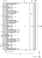
- FIG. 1 is a diagram showing an example of the top surface of a semiconductor device 100.
- FIG. 1 is a diagram showing an example of aa' cross section of a semiconductor device 100.
- FIG. 2 is a diagram showing an example of a bb' cross section of the semiconductor device 100.
- FIG. 1 is a diagram showing an example of a cc' cross section of the semiconductor device 100.
- FIG. 1 is a diagram showing an example of a dd′ cross section of the semiconductor device 100.
- FIG. 1A and 1B are diagrams illustrating modified examples of the upper surface of the semiconductor device 100.
- 1A and 1B are diagrams illustrating modified examples of the upper surface of the semiconductor device 100.
- 1A and 1B are diagrams illustrating modified examples of the upper surface of the semiconductor device 100.
- 1 is a diagram showing an example of an ee′ cross section of a semiconductor device 100.
- top one side in a direction parallel to the depth direction of the semiconductor substrate is referred to as "top” and the other side as “bottom.”
- bottom one side in a direction parallel to the depth direction of the semiconductor substrate
- top surface one surface is referred to as the top surface and the other surface is referred to as the bottom surface.
- the directions of "top,” “bottom,” “front,” and “back” are not limited to the direction of gravity or the direction in which the semiconductor device is attached to a substrate or the like when mounted.
- the orthogonal coordinate axes merely identify the relative positions of components, and do not limit a specific direction.
- the Z-axis does not limit the height direction relative to the ground.
- the +Z-axis direction and the -Z-axis direction are opposite directions.
- the Z-axis direction is described without indicating positive or negative, it means the direction parallel to the +Z-axis and -Z-axis.
- the plane parallel to the top surface of the semiconductor substrate is referred to as the XY plane, and the orthogonal axes parallel to the top and bottom surfaces of the semiconductor substrate are referred to as the X-axis and Y-axis.
- the axis perpendicular to the top and bottom surfaces of the semiconductor substrate is referred to as the Z-axis.
- the depth direction of the semiconductor substrate may be referred to as the Z-axis.
- the case where the semiconductor substrate is viewed in the Z-axis direction is referred to as a planar view.
- the direction parallel to the top and bottom surfaces of the semiconductor substrate, including the X-axis and Y-axis may be referred to as the horizontal direction.
- the first conductivity type is N-type and the second conductivity type is P-type, but the first conductivity type may be P-type and the second conductivity type may be N-type.
- the conductivity types of the substrate, layer, region, etc. in each embodiment will be of opposite polarity.
- the conductivity type of a doped region doped with impurities is described as P type or N type.
- impurities may specifically mean either N type donors or P type acceptors, and may be described as dopants.
- doping means introducing donors or acceptors into a semiconductor substrate to make it a semiconductor that exhibits N type conductivity or a semiconductor that exhibits P type conductivity.
- doping concentration refers to the donor concentration or acceptor concentration in thermal equilibrium.
- FIG. 1A shows an example of the top surface of a semiconductor device 100.
- the semiconductor device 100 in this example is a semiconductor chip that includes at least a transistor portion 70.
- the semiconductor device 100 is a reverse conducting IGBT (RC-IGBT).
- the transistor section 70 is a region obtained by projecting the collector region 22 provided on the back side of the semiconductor substrate 10 onto the upper surface of the semiconductor substrate 10.
- the collector region 22 will be described later.
- the transistor section 70 includes a transistor such as an IGBT.
- an edge termination structure may be provided in the region on the negative side in the Y-axis direction of the semiconductor device 100 in this example.
- the edge termination structure relieves electric field concentration on the upper surface side of the semiconductor substrate 10.
- the edge termination structure has, for example, a guard ring, a field plate, a resurf, or a structure combining these. Note that, for convenience, in this example, the edge on the negative side in the Y-axis direction is described, but the same applies to the other edges of the semiconductor device 100.
- the edge termination structure may be provided to surround an active region including a transistor portion 70.
- the semiconductor substrate 10 may be a silicon substrate, a silicon carbide substrate, a nitride semiconductor substrate such as gallium nitride, etc.
- the semiconductor substrate 10 in this example is a silicon substrate.
- the semiconductor device 100 of this example includes a gate trench portion 40, a dummy trench portion 30, an emitter region 12, a base region 14, and a well region 17 on the front surface 21 of the semiconductor substrate 10.
- the front surface 21 will be described later.
- the semiconductor device 100 of this example also includes an emitter electrode 52 and a gate metal layer 50 provided above the front surface 21 of the semiconductor substrate 10.
- the emitter electrode 52 is provided above the gate trench portion 40, the dummy trench portion 30, the emitter region 12, the base region 14, and the well region 17.
- the gate metal layer 50 is provided above the connection portion 25 and the well region 17.
- the emitter electrode 52 and the gate metal layer 50 are formed of a material containing a metal. At least a portion of the emitter electrode 52 may be formed of a metal such as aluminum (Al) or a metal alloy such as aluminum-silicon alloy (AlSi) or aluminum-silicon-copper alloy (AlSiCu). At least a portion of the gate metal layer 50 may be formed of a metal such as aluminum (Al) or a metal alloy such as aluminum-silicon alloy (AlSi) or aluminum-silicon-copper alloy (AlSiCu). The emitter electrode 52 and the gate metal layer 50 may have a barrier metal layer made of titanium or a titanium compound under the region made of aluminum or the like. The emitter electrode 52 and the gate metal layer 50 are provided separately from each other.
- the emitter electrode 52 and the gate metal layer 50 are provided above the semiconductor substrate 10 with the interlayer insulating film 38 in between.
- the interlayer insulating film 38 is omitted in FIG. 1A.
- the interlayer insulating film 38 has contact holes 54, 55, and 56 penetrating therethrough.
- the contact hole 55 electrically connects the gate metal layer 50 and the gate conductive portion in the transistor portion 70 via the connection portion 25.
- a plug layer made of tungsten or the like may be formed inside the contact hole 55.
- the contact hole 56 connects the emitter electrode 52 to the dummy conductive portion in the dummy trench portion 30.
- a plug layer made of tungsten or the like may be formed inside the contact hole 56.
- connection portion 25 is connected to the emitter electrode 52 or the front surface side metal layer such as the gate metal layer 50.
- the connection portion 25 is provided between the gate metal layer 50 and the gate conductive portion.
- the connection portion 25 in this example is provided extending in the X-axis direction and may be electrically connected to the gate conductive portion.
- the connection portion 25 may also be provided between the emitter electrode 52 and the dummy conductive portion.
- the connection portion 25 is a conductive material such as polysilicon doped with impurities.
- the connection portion 25 in this example is polysilicon (N+) doped with N-type impurities.
- the connection portion 25 is provided above the front surface 21 of the semiconductor substrate 10 via an insulating film such as an oxide film.
- the front surface 21 of the semiconductor substrate 10 is provided with a plurality of trench portions extending in a predetermined direction (in this example, the Y-axis direction) and arranged in a predetermined direction (in this example, the X-axis direction).
- the plurality of trench portions include gate trench portions 40 to which a gate potential is applied, and dummy trench portions 30 to which a potential different from the gate potential is applied.
- the gate trench portion 40 is an example of a plurality of trench portions extending in a predetermined extension direction on the front surface 21 side of the semiconductor substrate 10.
- the gate trench portions 40 are arranged at predetermined intervals along a predetermined arrangement direction (the X-axis direction in this example).
- the gate trench portion 40 in this example may have two extension portions 41 extending parallel to the front surface 21 of the semiconductor substrate 10 and along an extension direction perpendicular to the arrangement direction (the Y-axis direction in this example), and a connection portion 43 connecting the two extension portions 41.
- connection portion 43 is formed in a curved shape.
- the gate metal layer 50 may be electrically connected to the gate conductive portion via the connection portion 25.
- the dummy trench portion 30 is an example of a plurality of trench portions extending in a predetermined extension direction on the front surface 21 side of the semiconductor substrate 10.
- the dummy trench portion 30 is a trench portion electrically connected to the emitter electrode 52.
- the dummy trench portion 30 is arranged at predetermined intervals along a predetermined arrangement direction (the X-axis direction in this example).
- the dummy trench portion 30 in this example has an I-shape on the front surface 21 of the semiconductor substrate 10, but like the gate trench portion 40, it may have a U-shape on the front surface 21 of the semiconductor substrate 10. That is, the dummy trench portion 30 may have two extension portions 31 extending along the extension direction and a connection portion 33 connecting the two extension portions, as described later.
- the transistor section 70 in this example has a structure in which two gate trench sections 40 and two dummy trench sections 30 are arranged in a repeated manner. That is, the transistor section 70 in this example has gate trench sections 40 and dummy trench sections 30 in a 1:1 ratio. For example, the transistor section 70 has one dummy trench section 30 between two extension sections 41.
- the ratio of the gate trench portions 40 to the dummy trench portions 30 is not limited to this example.
- the ratio of the gate trench portions 40 may be greater than the ratio of the dummy trench portions 30, and the ratio of the dummy trench portions 30 may be greater than the ratio of the gate trench portions 40.
- the ratio of the gate trench portions 40 to the dummy trench portions 30 may be 2:3 or 2:4.
- the transistor portion 70 may not have dummy trench portions 30, with all trench portions being gate trench portions 40.
- the well region 17 is a second conductivity type region provided on the front surface 21 side of the semiconductor substrate 10 relative to the drift region 18 described later.
- the well region 17 is an example of a well region provided on the peripheral side of the active region.
- the well region 17 is a P+ type, for example.
- the well region 17 is formed in a predetermined range from the end of the active region on the side where the gate metal layer 50 is provided.
- the diffusion depth of the well region 17 may be deeper than the depth of the gate trench portion 40 and the dummy trench portion 30.
- a portion of the gate trench portion 40 and the dummy trench portion 30 on the gate metal layer 50 side is formed in the well region 17.
- the bottom of the end of the gate trench portion 40 and the dummy trench portion 30 in the extension direction may be covered by the well region 17.
- the contact hole 54 is formed above the emitter region 12 in the transistor section 70.
- the contact hole 54 is not provided above the well region 17 provided at both ends in the Y-axis direction.
- One or more contact holes 54 may be formed to penetrate the interlayer insulating film and reach the inside of the semiconductor substrate 10.
- the one or more contact holes 54 may be provided extending in the extension direction, or may be provided extending in a direction different from the extension direction.
- the trench contact portion 26 is provided in the contact hole 54.
- the trench contact portion 26 is provided from the upper surface of the interlayer insulating film, penetrating the front surface 21 of the semiconductor substrate 10, to the inside of the semiconductor substrate 10.
- the trench contact portion 26 has a conductive material filled in the contact hole 54.
- the trench contact portion 26 may have the same material as the emitter electrode 52.
- the trench contact portion 26 may include a tungsten plug, and may include a barrier metal such as Ti or TiN.
- the trench contact portion 26 has a main trench contact 27 and a secondary trench contact 28.
- the main trench contact 27 is provided so as to extend in the trench extension direction of the multiple trench portions when viewed from above. Details of the main trench contact 27 will be described later.
- the sub-trench contacts 28 are provided so as to extend from the main trench contact 27 in a direction different from the trench extension direction when viewed from above.
- the sub-trench contacts 28 may be provided so as to extend in the trench arrangement direction of the multiple trench portions, or may be provided so as to extend in a direction having a predetermined angle with respect to the trench arrangement direction.
- the sub-trench contacts 28 may be provided so as to extend in different directions from each other.
- the sub-trench contacts 28 may have a curved portion.
- the sub-trench contact 28 may be provided across the main trench contact 27 in the trench arrangement direction.
- the sub-trench contact 28 is provided so as not to contact adjacent trench portions. This makes it possible to prevent a short circuit between the emitter electrode 52 and the gate metal layer 50.
- the sub-trench contacts 28 may be provided in multiple locations for the main trench contact 27 in the mesa portion 71.
- the multiple sub-trench contacts 28 are provided above the emitter region 12 that extends in the trench extension direction of the multiple trench portions.
- a plug region 73 which will be described later, is provided on the lower surface of the trench contact portion 26.
- holes can be extracted from the semiconductor substrate 10, improving the latch-up resistance of the semiconductor device 100.
- Mesa portion 71 is a mesa portion provided adjacent to a trench portion in a plane parallel to front surface 21 of semiconductor substrate 10.
- a mesa portion is a portion of semiconductor substrate 10 sandwiched between two adjacent trench portions, and may be a portion from front surface 21 of semiconductor substrate 10 to the deepest bottom of each trench portion.
- the extension portion of each trench portion may be considered as one trench portion. In other words, the area sandwiched between two extension portions may be considered as a mesa portion.
- the mesa portion 71 is provided in the transistor portion 70 adjacent to at least one of the dummy trench portion 30 or the gate trench portion 40.
- the mesa portion 71 has a well region 17, an emitter region 12, and a base region 14 on the front surface 21 of the semiconductor substrate 10.
- the emitter region 12 is provided extending in the trench extension direction of the multiple trench portions.
- the base region 14 is a region of a second conductivity type provided on the front surface 21 side of the semiconductor substrate 10.
- the base region 14 is, for example, P- type.
- the doping concentration of the base region 14 may be 1E14 cm -3 or more and 1E18 cm -3 or less.
- the base region 14 may be provided below the emitter region 12.
- the base region 14 is provided in contact with the gate trench portion 40.
- the base region 14 may be provided in contact with the dummy trench portion 30.
- the base region 14 may be provided on both ends of the mesa portion 71 in the Y-axis direction on the front surface 21 of the semiconductor substrate 10. Note that FIG. 1A shows only one end of the base region 14 in the Y-axis direction.
- the emitter region 12 is a region of the first conductivity type having a higher doping concentration than the drift region 18.
- the emitter region 12 is, for example, N+ type.
- An example of a dopant for the emitter region 12 may be arsenic (As).
- the emitter region 12 is provided in contact with the gate trench portion 40 on the front surface 21 of the mesa portion 71.
- the emitter region 12 may be provided extending in the X-axis direction from one of the two trench portions sandwiching the mesa portion 71 to the other.
- the emitter region 12 may also be provided below the contact hole 54.
- the emitter region 12 may or may not be in contact with the dummy trench portion 30.
- the emitter region 12 is in contact with the dummy trench portion 30.
- no high concentration second conductivity type region is provided on the front surface 21 of the semiconductor substrate 10.
- an emitter region 12 is provided on the front surface 21 over the entire region of the mesa portion 71 that operates as a transistor.
- the saturation current can be improved when the semiconductor device 100 is miniaturized.
- FIG. 1B shows an example of the a-a' cross section in FIG. 1A.
- the a-a' cross section is an XZ plane that does not pass through the sub-trench contact 28.
- the semiconductor device 100 of this example has a semiconductor substrate 10 in which the emitter region 12, base region 14, accumulation region 16, drift region 18, buffer region 20, collector region 22 and plug region 73 are provided, an interlayer insulating film 38, an emitter electrode 52 and a collector electrode 24.
- the drift region 18 is a region of a first conductivity type provided in the semiconductor substrate 10.
- the drift region 18 is, as an example, N-type.
- the drift region 18 may be a region remaining in the semiconductor substrate 10 without other doped regions being formed therein.
- the doping concentration of the drift region 18 may be the doping concentration of the semiconductor substrate 10.
- the buffer region 20 is a region of a first conductivity type provided on the back surface 23 side of the semiconductor substrate 10 relative to the drift region 18.
- the buffer region 20 is, as an example, an N-type.
- the doping concentration of the buffer region 20 is higher than the doping concentration of the drift region 18.
- the buffer region 20 may function as a field stop layer that prevents the depletion layer spreading from the lower surface side of the base region 14 from reaching the collector region 22 of the second conductivity type.
- the buffer region 20 may be omitted.
- the collector region 22 is provided on the rear surface 23 of the semiconductor substrate 10 in the transistor section 70.
- the collector region 22 is a region of a second conductivity type having a higher doping concentration than the base region 14.
- the collector region 22 is, as an example, a P+ type.
- the collector electrode 24 is an example of a backside metal layer provided in contact with the backside 23 of the semiconductor substrate 10.
- the emitter electrode 52 is formed above the semiconductor substrate 10 and the interlayer insulating film 38.
- the accumulation region 16 is provided below the base region 14 in the depth direction of the semiconductor substrate 10, and is a region of a first conductivity type with a higher doping concentration than the drift region 18.
- the accumulation region 16 is an N+ type, for example.
- One or more gate trench portions 40 and one or more dummy trench portions 30 are provided on the front surface 21.
- Each trench portion is provided from the front surface 21 to the drift region 18. In the regions where at least one of the emitter region 12, the base region 14, and the accumulation region 16 is provided, each trench portion also penetrates these regions to reach the drift region 18.
- the trench portion penetrating the doped region is not limited to being manufactured in the order of forming the doped region and then the trench portion.
- the trench portion penetrating the doped region also includes a case where a doped region is formed between the trench portions after the trench portions are formed.
- the gate trench portion 40 has a gate trench, a gate insulating film 42, and a gate conductive portion 44 formed on the front surface 21.
- the gate insulating film 42 is formed to cover the inner wall of the gate trench.
- the gate insulating film 42 may be formed by oxidizing or nitriding the semiconductor on the inner wall of the gate trench.
- the gate conductive portion 44 is formed inside the gate trench, further inside than the gate insulating film 42.
- the gate insulating film 42 insulates the gate conductive portion 44 from the semiconductor substrate 10.
- the gate conductive portion 44 is formed of a conductive material such as polysilicon.
- the gate trench portion 40 is covered by an interlayer insulating film 38 on the front surface 21.
- the gate conductive portion 44 includes a region facing the adjacent base region 14 on the mesa portion 71 side across the gate insulating film 42 in the depth direction of the semiconductor substrate 10. When a predetermined voltage is applied to the gate conductive portion 44, a channel is formed by an electron inversion layer on the surface layer of the interface of the base region 14 that contacts the gate trench.
- the dummy trench portion 30 may have the same structure as the gate trench portion 40.
- the dummy trench portion 30 has a dummy trench, a dummy insulating film 32, and a dummy conductive portion 34 formed on the front surface 21 side.
- the dummy insulating film 32 is formed to cover the inner wall of the dummy trench.
- the dummy conductive portion 34 is formed inside the dummy trench and is formed further inward than the dummy insulating film 32.
- the dummy insulating film 32 insulates the dummy conductive portion 34 from the semiconductor substrate 10.
- the dummy trench portion 30 is covered by an interlayer insulating film 38 on the front surface 21.
- the interlayer insulating film 38 is provided on the front surface 21.
- An emitter electrode 52 is provided above the interlayer insulating film 38.
- the interlayer insulating film 38 is provided with one or more trench contact portions 26 for electrically connecting the emitter electrode 52 to the semiconductor substrate 10. That is, the trench contact portion 26 is provided in a mesa portion between the multiple trench portions.
- the contact holes 55 and 56 may also be provided penetrating the interlayer insulating film 38, similar to the trench contact portion 26.
- the main trench contact 27 electrically connects the emitter electrode 52 and the semiconductor substrate 10.
- the depth of the lower end of the main trench contact 27 may be located deeper than the depth of the lower end of the emitter region 12, and may be the same as the depth of the lower end of the emitter region 12.
- the depth of the lower end of the main trench contact 27 may be located shallower than the lower end of the base region 14.
- the main trench contact 27 may have a predetermined width in the trench arrangement direction of the multiple trench portions.
- the width of the main trench contact 27 may be the width at the lower end of the main trench contact 27, or may be the width from one sidewall to the other sidewall of the main trench contact 27 on the front surface 21 of the semiconductor substrate 10, or may be the opening width of the contact hole 54 at the upper end of the interlayer insulating film 38.
- the width of the main trench contact 27 may be the width from one sidewall to the other sidewall of the main trench contact 27 at any depth in the trench arrangement direction of the multiple trench portions.
- the width W27 of the main trench contact 27 is the width at the lower end of the main trench contact 27.
- the width of the main trench contact 27 in the trench arrangement direction of the multiple trench portions is the same as the width of the sub-trench contact 28 in the trench extension direction of the multiple trench portions described below.
- the width of the main trench contact 27 in the trench arrangement direction of the multiple trench portions may be larger or smaller than the width of the sub-trench contact 28 in the trench extension direction of the multiple trench portions.
- the width of the main trench contact 27 in the trench arrangement direction of the multiple trench portions may be 0.1 ⁇ m or more and 0.8 ⁇ m or less.
- the plug region 73 is a region of a second conductivity type provided in contact with the lower end of the trench contact portion 26.
- the doping concentration of the plug region 73 is higher than the doping concentration of the base region 14.
- the plug region 73 is, for example, a P+ type.
- the doping concentration of the plug region 73 may be 1E17 cm ⁇ 3 or more and may be 1E20 cm ⁇ 3 or less.
- the plug region 73 may be provided so as to cover the bottom and part of the sidewall of the trench contact portion 26.
- the plug region 73 may be provided apart from the emitter region 12, or may be provided in contact with the emitter region 12. In this example, the plug region 73 is provided in contact with the emitter region 12.
- the plug region 73 may be provided at a distance from adjacent trench portions in the trench arrangement direction of the multiple trench portions.
- the plug region 73 may be provided at a distance from the gate trench portion 40. This makes the gate voltage required to form a channel inversion region constant, and makes it possible to uniformize the characteristics of the semiconductor device 100.
- the plug region 73 may be formed by injecting a dopant through the contact hole 54.
- the plug region 73 may be provided on the underside of both the main trench contact 27 and the sub-trench contact 28. Also, the plug region 73 may be provided first, and then the trench contact portion 26 having the main trench contact 27 and the sub-trench contact 28 may be provided.
- FIG. 1C shows an example of the b-b' cross section in FIG. 1A.
- the b-b' cross section is an XZ plane passing through the main trench contact 27 and the sub-trench contact 28. The differences from the cross section shown in FIG. 1B will be explained using FIG. 1C.
- the sub-trench contact 28 electrically connects the emitter electrode 52 and the semiconductor substrate 10.
- the depth of the lower end of the sub-trench contact 28 may be the same as the depth of the lower end of the main trench contact 27.
- FIG. 1C for the purpose of explanation, the position of the main trench contact 27 is shown by a dotted line.
- a plug region 73 is also provided below the sub-trench contact 28.
- the plug region 73 may cover the bottom surface and part of the sidewall of the sub-trench contact 28.
- the sub-trench contact 28 is provided at a distance from the trench portion in the trench arrangement direction of the multiple trench portions.
- the sub-trench contact 28 is provided to have a predetermined distance dx from an adjacent trench portion in the trench arrangement direction.
- the predetermined distance dx may be the shortest distance between the sub-trench contact 28 and the trench portion.
- the shortest distance between the sub-trench contact 28 and the trench portion is the distance from the sidewall of the adjacent trench portion to the sidewall of the sub-trench contact 28 on the upper surface of the interlayer insulating film 38.
- the shortest distance between the sub-trench contact 28 and the trench portion may be the distance from the sidewall of the adjacent trench portion to the sidewall of the sub-trench contact 28 at the same depth. If the sidewall of the sub-trench contact 28 has an inverse taper, the shortest distance between the sub-trench contact 28 and the trench portion may be the distance from the sidewall of the adjacent trench portion to the lower end of the sidewall of the sub-trench contact 28.
- the shortest distance between the sub-trench contact 28 and the trench portion in the trench arrangement direction of the multiple trench portions may be 0.1 ⁇ m or more and 0.7 ⁇ m or less.
- FIG. 1D shows an example of the c-c' cross section in FIG. 1A.
- the c-c' cross section is a YZ plane along the main trench contact 27.
- the main trench contact 27 is provided to a position deeper than the depth of the bottom end of the emitter region 12, so the emitter region 12 is not shown in the cross section shown in FIG. 1D.
- the plug region 73 is provided along the main trench contact 27, extending in the trench extension direction of the multiple trench portions.
- the plug region 73 may be provided discretely so as to cover a portion of the lower surface of the main trench contact 27, or may be provided continuously so as to cover the entire lower surface of the main trench contact 27.
- FIG. 1E shows an example of the dd' cross section in FIG. 1A.
- the dd' cross section is a YZ plane that does not pass through the main trench contact 27, but passes through the sub-trench contact 28.
- the multiple sub-trench contacts 28 are provided at a predetermined interval d28 in the trench extension direction of the multiple trench portions.
- the predetermined interval d28 may be 0.1 ⁇ m or more and 5.0 ⁇ m or less.
- the sub-trench contacts 28 have a predetermined width W28 in the trench extension direction of the trench portions.
- the width of the sub-trench contact 28 may be the width at the bottom end of the sub-trench contact 28, or may be the width from one sidewall to the other sidewall of the sub-trench contact 28 on the front surface 21 of the semiconductor substrate 10, or may be the opening width of the contact hole 54 at the top end of the interlayer insulating film 38.
- the width of the sub-trench contact 28 may be the width from one sidewall to the other sidewall of the sub-trench contact 28 at any depth in the trench extension direction of the trench portions.
- the width W28 of the sub-trench contact 28 is the width at the bottom end of the sub-trench contact 28.
- the width W28 of the sub-trench contact 28 in the trench extension direction of the multiple trench portions may be the same as or different from the width W27 of the main trench contact 27 in the trench arrangement direction of the multiple trench portions.
- the width W28 of the sub-trench contact 28 in the trench extension direction of the multiple trench portions may be 90% or more and 110% or less of the width W27 of the main trench contact 27 in the trench arrangement direction of the multiple trench portions.
- the width W28 of the sub-trench contact 28 in the trench extension direction of the multiple trench portions may be 0.1 ⁇ m or more and 0.8 ⁇ m or less.
- the plug regions 73 are provided to have a predetermined distance d73 in the trench extension direction of the multiple trench portions.
- the predetermined distance d73 may be 0.1 ⁇ m or more and 0.5 ⁇ m or less.
- the plug regions 73 provided on the lower surfaces of adjacent sub-trench contacts 28 are provided so as not to come into contact with each other in the trench extension direction of the multiple trench portions.
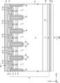
- FIG. 2 is a diagram showing a modified top surface of the semiconductor device 100. The differences from the semiconductor device 100 shown in FIG. 1A will be explained using FIG. 2.
- the base region 14 is also provided in the region of the mesa portion 71 that operates as a transistor. That is, in the mesa portion 71, the emitter region 12 and the base region 14 may be provided alternately in the trench extension direction of the multiple trench portions on the front surface 21 of the semiconductor substrate 10.
- the emitter region 12 and the base region 14 may be provided to have predetermined widths Wn and Wp.
- the widths Wn and Wp may be the same or different for each of the discretely provided emitter regions 12 and base regions 14.
- the widths Wn and Wp may be the same or different.
- the ratio Wn:Wp of the widths Wn and Wp may be set to any ratio between 3:1 and 1:8. In this example, the ratio Wn:Wp of the widths Wn and Wp is approximately 1:3. By adjusting the ratio of the widths Wn and Wp, the saturation current of the semiconductor device 100 can be adjusted to match the required characteristics.
- the main trench contact 27 is provided above the emitter regions 12 and base regions 14 that are alternately provided in the trench extension direction, and extends in the trench extension direction.
- the main trench contact 27 is provided extending into the emitter regions 12 and base regions 14 in the depth direction of the semiconductor substrate 10, and electrically connects the emitter regions 12 and base regions 14 to the emitter electrode 52.
- the sub-trench contact 28 is provided above the base region 14.
- the sub-trench contact 28 is not provided above the emitter region 12.
- the region on the front surface 21 of the semiconductor substrate 10 where the base region 14 is provided is a region that does not operate as a transistor, so by providing the sub-trench contact 28 in this manner, the latch-up resistance can be improved without reducing the operating efficiency of the semiconductor device 100.
- no region of the second conductivity type is provided other than the base region 14. This eliminates the need for an ion implantation process to separately form a region of the second conductivity type, thereby reducing the manufacturing cost of the semiconductor device 100.
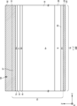
- FIG. 3 is a diagram showing a modified top surface of the semiconductor device 100. The differences from the semiconductor device 100 shown in FIG. 1A will be explained using FIG. 3.
- the multiple trench portions may include a first trench portion and a second trench portion adjacent to the first trench portion.
- the first trench portion is a gate trench portion 40 and the second trench portion is a dummy trench portion 30.
- the first trench portion may be a dummy trench portion 30 and the second trench portion may be a gate trench portion 40.
- the sub-trench contacts 28 may include a first sub-trench contact 281 that extends from the main trench contact 27 toward the first trench portion in the trench arrangement direction of the multiple trench portions and terminates without reaching the first trench portion.
- the sub-trench contacts 28 may include a second sub-trench contact 282 that extends from the main trench contact 27 toward the second trench portion in the trench arrangement direction of the multiple trench portions and terminates without reaching the second trench portion.
- the first sub-trench contacts 281 may be provided to have a predetermined interval d281 in the trench extension direction of the multiple trench portions.
- the second sub-trench contacts 282 may be provided to have a predetermined interval d282 in the trench extension direction of the multiple trench portions.
- the interval d281 and the interval d282 may be the same or different.
- the first sub-trench contacts 281 and the second sub-trench contacts 282 may be provided in the same number or different numbers.
- the first sub-trench contacts 281 and the second sub-trench contacts 282 may be provided alternately in the trench extension direction of the multiple trench portions. In the trench extension direction of the multiple trench portions, one second sub-trench contact 282 may be provided between two first sub-trench contacts 281, and one first sub-trench contact 281 may be provided between two second sub-trench contacts 282.
- the first sub-trench contact 281 may be provided at a position that divides the distance d282 between two adjacent second sub-trench contacts 282 at any ratio. In this example, the first sub-trench contact 281 is provided at the midpoint of the distance d282 between two adjacent second sub-trench contacts 282.
- the second sub-trench contact 282 may be provided at a position that divides the distance d281 between two adjacent first sub-trench contacts 281 at any ratio.
- the second sub-trench contact 282 is provided at the midpoint of the distance d281 between two adjacent first sub-trench contacts 281.
- the first sub-trench contact 281 and the second sub-trench contact 282 may be provided at symmetrical positions on either side of the main trench contact 27.
- the first sub-trench contact 281 and the second sub-trench contact 282 may be connected and treated as one sub-trench contact 28.
- the saturation current of the semiconductor device 100 can be adjusted to meet the required performance.
- Plug regions 73 may also be provided in the first sub-trench contact 281 and the second sub-trench contact 282. This can improve the latch-up resistance of the semiconductor device 100.
- the modified example shown in FIG. 3 may be combined with the modified example shown in FIG. 2. That is, in an embodiment in which emitter regions 12 and base regions 14 are alternately provided in the trench extension direction of multiple trench portions on the front surface 21 of the semiconductor substrate 10, the first sub-trench contact 281 and the second sub-trench contact 282 may be provided above the base region 14, and do not have to be provided above the emitter region 12.
- FIG. 4A is a diagram showing a modified example of the top surface of the semiconductor device 100.
- the semiconductor device 100 of this example is an RC-IGBT that further includes a diode portion 80 having an anode region 19 on the front surface 21 of the semiconductor substrate 10.
- the diode section 80 is a region obtained by projecting a cathode region 82 provided on the rear surface 23 side of the semiconductor substrate 10 onto the upper surface of the semiconductor substrate 10.
- a collector region 22 may be provided in the area of the rear surface 23 of the semiconductor substrate 10 other than the cathode region 82.
- the mesa portion 81 is provided adjacent to the trench portion in a plane parallel to the front surface 21 of the semiconductor substrate 10.
- the mesa portion 81 is provided adjacent to two dummy trench portions 30 in the diode portion 80.
- the mesa portion 81 has a well region 17, a base region 14, and an anode region 19 on the front surface 21 of the semiconductor substrate 10.
- the anode region 19 is provided extending in the trench extension direction of the multiple trench portions.
- Mesa portion 91 is a mesa portion provided adjacent to a trench portion in a plane parallel to front surface 21 of semiconductor substrate 10.
- Mesa portion 91 is provided adjacent to at least one of dummy trench portion 30 or gate trench portion 40 in transistor portion 70.
- the structure of mesa portion 91 on front surface 21 of semiconductor substrate 10 is the same as the structure of mesa portion 81 on front surface 21 of semiconductor substrate 10.
- the contact hole 54 may also be provided above the diode section 80 and the boundary section 90. That is, the trench contact section 26 may be provided above the diode section 80 and the boundary section 90, and the main trench contact 27 and the sub-trench contact 28 may be provided above the anode region 19. By providing the main trench contact 27 and the sub-trench contact 28 above the diode section 80, the contact properties in the diode section 80 are improved, and the forward voltage Vf of the diode section 80 can be improved.
- the diode section 80 only the main trench contact 27 may be provided, and the sub-trench contact 28 may not be provided. This eliminates the need for a tungsten plug to form the sub-trench contact 28, thereby reducing the manufacturing cost of the semiconductor device 100.
- FIG. 4B shows an example of the ee' cross section in FIG. 4A.
- the ee' cross section is an XZ plane that does not pass through the sub-trench contact 28. The differences from the cross section shown in FIG. 1B will be explained using FIG. 4B.
- the plug region 73 is also provided in the diode portion 80 and the boundary portion 90.
- the plug region 73 is provided on the lower surface of the trench contact portion 26 in the diode portion 80 and the boundary portion 90. That is, the plug region 73 may be provided so as to cover the bottom and part of the sidewall of the main trench contact 27 and the sub-trench contact 28 in the diode portion 80 and the boundary portion 90.
- the plug region 73 may be provided continuously in the trench extension direction of the multiple trench portions in the diode portion 80 and the boundary portion 90, or may be provided discretely. By providing the plug region 73 in the diode portion 80 and the boundary portion 90, the efficiency of extracting holes from the semiconductor substrate 10 can be improved, and the latch-up resistance of the semiconductor device 100 can be improved.
- emitter regions 12 and base regions 14 may be provided alternately in the trench extension direction of the multiple trench sections on the front surface 21 of the semiconductor substrate 10 in the transistor section 70, and the sub-trench contact 28 may be provided above the base region 14, but need not be provided above the emitter region 12.
Landscapes
- Electrodes Of Semiconductors (AREA)
Priority Applications (3)
| Application Number | Priority Date | Filing Date | Title |
|---|---|---|---|
| DE112024000244.7T DE112024000244T5 (de) | 2023-07-06 | 2024-05-21 | Halbleitervorrichtung |
| JP2025531413A JPWO2025009277A1 (https=) | 2023-07-06 | 2024-05-21 | |
| US19/245,388 US20250318254A1 (en) | 2023-07-06 | 2025-06-22 | Semiconductor device |
Applications Claiming Priority (2)
| Application Number | Priority Date | Filing Date | Title |
|---|---|---|---|
| JP2023-111372 | 2023-07-06 | ||
| JP2023111372 | 2023-07-06 |
Related Child Applications (1)
| Application Number | Title | Priority Date | Filing Date |
|---|---|---|---|
| US19/245,388 Continuation US20250318254A1 (en) | 2023-07-06 | 2025-06-22 | Semiconductor device |
Publications (1)
| Publication Number | Publication Date |
|---|---|
| WO2025009277A1 true WO2025009277A1 (ja) | 2025-01-09 |
Family
ID=94171805
Family Applications (1)
| Application Number | Title | Priority Date | Filing Date |
|---|---|---|---|
| PCT/JP2024/018628 Ceased WO2025009277A1 (ja) | 2023-07-06 | 2024-05-21 | 半導体装置 |
Country Status (4)
| Country | Link |
|---|---|
| US (1) | US20250318254A1 (https=) |
| JP (1) | JPWO2025009277A1 (https=) |
| DE (1) | DE112024000244T5 (https=) |
| WO (1) | WO2025009277A1 (https=) |
Citations (7)
| Publication number | Priority date | Publication date | Assignee | Title |
|---|---|---|---|---|
| JP2013115158A (ja) * | 2011-11-28 | 2013-06-10 | Hitachi Ltd | 4h−SiC半導体素子及び半導体装置 |
| JP2017028244A (ja) * | 2015-07-15 | 2017-02-02 | 富士電機株式会社 | 半導体装置 |
| WO2021010000A1 (ja) * | 2019-07-12 | 2021-01-21 | 富士電機株式会社 | 半導体装置 |
| JP2021027140A (ja) * | 2019-08-02 | 2021-02-22 | 株式会社東芝 | 半導体装置、インバータ回路、駆動装置、車両、及び、昇降機 |
| JP2023019322A (ja) * | 2021-07-29 | 2023-02-09 | 富士電機株式会社 | 半導体装置 |
| JP2023082869A (ja) * | 2021-12-03 | 2023-06-15 | 株式会社デンソー | 半導体装置 |
| WO2023105834A1 (ja) * | 2021-12-08 | 2023-06-15 | 富士電機株式会社 | 半導体装置および半導体装置の製造方法 |
-
2024
- 2024-05-21 DE DE112024000244.7T patent/DE112024000244T5/de active Pending
- 2024-05-21 JP JP2025531413A patent/JPWO2025009277A1/ja active Pending
- 2024-05-21 WO PCT/JP2024/018628 patent/WO2025009277A1/ja not_active Ceased
-
2025
- 2025-06-22 US US19/245,388 patent/US20250318254A1/en active Pending
Patent Citations (7)
| Publication number | Priority date | Publication date | Assignee | Title |
|---|---|---|---|---|
| JP2013115158A (ja) * | 2011-11-28 | 2013-06-10 | Hitachi Ltd | 4h−SiC半導体素子及び半導体装置 |
| JP2017028244A (ja) * | 2015-07-15 | 2017-02-02 | 富士電機株式会社 | 半導体装置 |
| WO2021010000A1 (ja) * | 2019-07-12 | 2021-01-21 | 富士電機株式会社 | 半導体装置 |
| JP2021027140A (ja) * | 2019-08-02 | 2021-02-22 | 株式会社東芝 | 半導体装置、インバータ回路、駆動装置、車両、及び、昇降機 |
| JP2023019322A (ja) * | 2021-07-29 | 2023-02-09 | 富士電機株式会社 | 半導体装置 |
| JP2023082869A (ja) * | 2021-12-03 | 2023-06-15 | 株式会社デンソー | 半導体装置 |
| WO2023105834A1 (ja) * | 2021-12-08 | 2023-06-15 | 富士電機株式会社 | 半導体装置および半導体装置の製造方法 |
Also Published As
| Publication number | Publication date |
|---|---|
| JPWO2025009277A1 (https=) | 2025-01-09 |
| US20250318254A1 (en) | 2025-10-09 |
| DE112024000244T5 (de) | 2025-08-21 |
Similar Documents
| Publication | Publication Date | Title |
|---|---|---|
| JP7655413B2 (ja) | 半導体装置 | |
| US20220271152A1 (en) | Semiconductor device and manufacturing method thereof | |
| JP6614326B2 (ja) | 半導体装置 | |
| JP7803330B2 (ja) | 半導体装置および半導体装置の製造方法 | |
| JP7666650B2 (ja) | 半導体装置 | |
| US10535761B2 (en) | Semiconductor device including a mesa portion including an emitter region having a varied width | |
| CN110047918B (zh) | 半导体装置 | |
| JP6958011B2 (ja) | 半導体装置および半導体装置の製造方法 | |
| JP7750090B2 (ja) | 半導体装置およびその製造方法 | |
| JPWO2019244485A1 (ja) | 半導体装置の製造方法および半導体装置 | |
| CN111247639A (zh) | 半导体装置 | |
| US20240088221A1 (en) | Semiconductor device | |
| US12439622B2 (en) | Semiconductor device and manufacturing method of semiconductor device | |
| JP7732510B2 (ja) | 半導体装置 | |
| WO2025009277A1 (ja) | 半導体装置 | |
| US20250254982A1 (en) | Semiconductor device | |
| WO2024241741A1 (ja) | 半導体装置および半導体装置の製造方法 | |
| JP2025099553A (ja) | 半導体装置 | |
| JP2025009216A (ja) | 半導体装置 | |
| WO2024185313A1 (ja) | 半導体装置および半導体装置の製造方法 | |
| JP2025187739A (ja) | 半導体装置 | |
| JP2024009540A (ja) | 半導体装置 | |
| WO2024214461A1 (ja) | 半導体装置 |
Legal Events
| Date | Code | Title | Description |
|---|---|---|---|
| WWE | Wipo information: entry into national phase |
Ref document number: 2025531413 Country of ref document: JP |
|
| WWE | Wipo information: entry into national phase |
Ref document number: 112024000244 Country of ref document: DE |
|
| WWP | Wipo information: published in national office |
Ref document number: 112024000244 Country of ref document: DE |