WO2025009269A1 - 積層セラミックコンデンサ - Google Patents
積層セラミックコンデンサ Download PDFInfo
- Publication number
- WO2025009269A1 WO2025009269A1 PCT/JP2024/017924 JP2024017924W WO2025009269A1 WO 2025009269 A1 WO2025009269 A1 WO 2025009269A1 JP 2024017924 W JP2024017924 W JP 2024017924W WO 2025009269 A1 WO2025009269 A1 WO 2025009269A1
- Authority
- WO
- WIPO (PCT)
- Prior art keywords
- glass
- external electrode
- electrode film
- ceramic body
- silicon
- Prior art date
- Legal status (The legal status is an assumption and is not a legal conclusion. Google has not performed a legal analysis and makes no representation as to the accuracy of the status listed.)
- Ceased
Links
Images


Classifications
-
- H—ELECTRICITY
- H01—ELECTRIC ELEMENTS
- H01G—CAPACITORS; CAPACITORS, RECTIFIERS, DETECTORS, SWITCHING DEVICES, LIGHT-SENSITIVE OR TEMPERATURE-SENSITIVE DEVICES OF THE ELECTROLYTIC TYPE
- H01G4/00—Fixed capacitors; Processes of their manufacture
- H01G4/002—Details
- H01G4/228—Terminals
- H01G4/232—Terminals electrically connecting two or more layers of a stacked or rolled capacitor
- H01G4/2325—Terminals electrically connecting two or more layers of a stacked or rolled capacitor characterised by the material of the terminals
-
- H—ELECTRICITY
- H01—ELECTRIC ELEMENTS
- H01B—CABLES; CONDUCTORS; INSULATORS; SELECTION OF MATERIALS FOR THEIR CONDUCTIVE, INSULATING OR DIELECTRIC PROPERTIES
- H01B1/00—Conductors or conductive bodies characterised by the conductive materials; Selection of materials as conductors
- H01B1/20—Conductive material dispersed in non-conductive organic material
- H01B1/22—Conductive material dispersed in non-conductive organic material the conductive material comprising metals or alloys
-
- H—ELECTRICITY
- H01—ELECTRIC ELEMENTS
- H01G—CAPACITORS; CAPACITORS, RECTIFIERS, DETECTORS, SWITCHING DEVICES, LIGHT-SENSITIVE OR TEMPERATURE-SENSITIVE DEVICES OF THE ELECTROLYTIC TYPE
- H01G4/00—Fixed capacitors; Processes of their manufacture
- H01G4/002—Details
- H01G4/005—Electrodes
- H01G4/012—Form of non-self-supporting electrodes
-
- H—ELECTRICITY
- H01—ELECTRIC ELEMENTS
- H01G—CAPACITORS; CAPACITORS, RECTIFIERS, DETECTORS, SWITCHING DEVICES, LIGHT-SENSITIVE OR TEMPERATURE-SENSITIVE DEVICES OF THE ELECTROLYTIC TYPE
- H01G4/00—Fixed capacitors; Processes of their manufacture
- H01G4/002—Details
- H01G4/018—Dielectrics
- H01G4/06—Solid dielectrics
- H01G4/08—Inorganic dielectrics
- H01G4/12—Ceramic dielectrics
- H01G4/1209—Ceramic dielectrics characterised by the ceramic dielectric material
-
- H—ELECTRICITY
- H01—ELECTRIC ELEMENTS
- H01G—CAPACITORS; CAPACITORS, RECTIFIERS, DETECTORS, SWITCHING DEVICES, LIGHT-SENSITIVE OR TEMPERATURE-SENSITIVE DEVICES OF THE ELECTROLYTIC TYPE
- H01G4/00—Fixed capacitors; Processes of their manufacture
- H01G4/002—Details
- H01G4/228—Terminals
- H01G4/232—Terminals electrically connecting two or more layers of a stacked or rolled capacitor
-
- H—ELECTRICITY
- H01—ELECTRIC ELEMENTS
- H01G—CAPACITORS; CAPACITORS, RECTIFIERS, DETECTORS, SWITCHING DEVICES, LIGHT-SENSITIVE OR TEMPERATURE-SENSITIVE DEVICES OF THE ELECTROLYTIC TYPE
- H01G4/00—Fixed capacitors; Processes of their manufacture
- H01G4/002—Details
- H01G4/228—Terminals
- H01G4/248—Terminals the terminals embracing or surrounding the capacitive element, e.g. caps
-
- H—ELECTRICITY
- H01—ELECTRIC ELEMENTS
- H01G—CAPACITORS; CAPACITORS, RECTIFIERS, DETECTORS, SWITCHING DEVICES, LIGHT-SENSITIVE OR TEMPERATURE-SENSITIVE DEVICES OF THE ELECTROLYTIC TYPE
- H01G4/00—Fixed capacitors; Processes of their manufacture
- H01G4/30—Stacked capacitors
Definitions
- the present invention relates to a multilayer ceramic capacitor.
- One method for manufacturing terminal electrodes of multilayer ceramic capacitors is to apply a conductive paste, in which conductive powder such as copper and glass frit powder are dispersed in a vehicle, to a ceramic body, dry it, and sinter it at high temperature to form terminal electrodes that are electrically connected to the internal electrode layers.
- Patent Document 1 describes a method that uses glass frit powder that contains barium.
- barium-boron-silicon glass can have a lower softening point than boron-silicon glass.
- the lower softening point allows for the formation of a dense film.
- barium-boron-silicon glass is less likely to form a reaction layer at the interface with the ceramic body. Specifically, when the ceramic body contains barium, the barium-boron-silicon glass inhibits the barium from migrating out of the ceramic body, making it less likely to form a reaction layer. Therefore, barium-boron-silicon glass can achieve good adhesion to the ceramic body.
- barium-boron-silicon glass has low moisture resistance and can change or dissolve when it comes into contact with an acid plating solution. If the glass changes, the plating solution can seep into the terminal electrodes. If the plating solution seeps into the terminal electrodes, it can cause reflow defects. In addition, the moisture resistance of the terminal electrodes can decrease, reducing the reliability of the multilayer ceramic capacitor.
- the present invention aims to provide a multilayer ceramic capacitor that can provide moisture resistance to the terminal electrodes while maintaining good adhesion between the terminal electrodes and the ceramic body.
- the multilayer ceramic capacitor of the present invention is a multilayer ceramic capacitor comprising a ceramic body including a plurality of laminated dielectric layers and a plurality of laminated internal electrode layers, the ceramic body having a first main surface and a second main surface that face each other in a height direction, a first side surface and a second side surface that face each other in a width direction perpendicular to the height direction, and a first end surface and a second end surface that face each other in a length direction perpendicular to the height direction and the width direction, and a terminal electrode provided on the ceramic body and connected to a part of the internal electrode layers, the terminal electrode including an external electrode film that is in contact with the ceramic body, the external electrode film being made of at least a barium-boron-silicon glass, or a strontium-boron-silicon glass, or a barium-strontium-boron-silicon glass.
- the first glass is made of at least one of the above, and the second glass is made of a bismuth-based glass, and the first glass and the second glass form a glass domain within the external electrode film.
- the concentration ratio of bismuth to silicon is higher in the portion of the first glass domain that is exposed to the surface of the external electrode film than in the portion of the second glass domain that is exposed to the interface of the external electrode film with the ceramic body.
- the present invention provides a multilayer ceramic capacitor that can provide moisture resistance to the terminal electrodes while maintaining good adhesion between the terminal electrodes and the ceramic body.
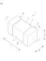
- FIG. 1 is a perspective view of a multilayer ceramic capacitor according to an embodiment of the present invention
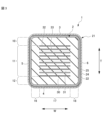
- 2 is a cross-sectional view taken along line II in FIG. 1.
- 2 is a cross-sectional view taken along line II-II of FIG. 1.
- 1 is an LT cross-sectional view of the multilayer ceramic capacitor in the vicinity of a second end face.
- FIG. 4 is a diagram showing a scanning electron microscope image of an external electrode film.
- FIG. 13 is a diagram showing a scanning electron microscope image of another external electrode film.
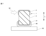
- FIG. 1 is a diagram showing a method for evaluating adhesion performance.
- FIG. 1 is a perspective view of a multilayer ceramic capacitor 1 according to an embodiment of the present invention.
- FIG. 1 shows a so-called two-terminal multilayer ceramic capacitor.
- the multilayer ceramic capacitor 1 of the present invention is not limited to a two-terminal multilayer ceramic capacitor.
- the multilayer ceramic capacitor 1 of the present invention may be a multi-terminal multilayer ceramic capacitor, such as a three-terminal one.
- the multilayer ceramic capacitor 1 includes a ceramic body 2 and terminal electrodes.
- the terminal electrodes include a first terminal electrode 20 and a second terminal electrode 21.
- the ceramic body 2 includes a plurality of laminated dielectric layers and a plurality of internal electrode layers.
- the shape of the ceramic body 2 is approximately a rectangular parallelepiped.
- the direction in which the dielectric layers and internal electrode layers are stacked is defined as the height direction T.
- the direction perpendicular to the height direction T is defined as the width direction W.
- the direction perpendicular to the height direction T and the width direction W is defined as the length direction L.
- one face is designated as the first main surface 3.
- the remaining face is designated as the second main surface 4.
- one face is designated as the first side surface 5.
- the remaining face is designated as the second side surface 6.
- one face is designated as the first end surface 7.
- the remaining face is designated as the second end surface 8.
- the cross section taken along line I-I in FIG. 1 is referred to as the LT cross section.
- the cross section taken along line II-II in FIG. 1 is referred to as the WT cross section.
- the portion where three faces of the ceramic body 2 intersect is called the corner of the ceramic body 2.
- the portion where two faces of the ceramic body 2 intersect is called the ridge of the ceramic body 2. It is preferable that the corners and ridges are rounded.
- the total number of dielectric layers laminated on the ceramic body 2 is preferably 15 or more and 2000 or less.
- the main material of the dielectric layers is a ceramic material.
- ceramic materials are dielectric ceramics whose main components are barium titanate, calcium titanate, strontium titanate, calcium zirconate, etc.
- the ceramic material may be a dielectric ceramic in which secondary components such as manganese compounds, iron compounds, chromium compounds, cobalt compounds, nickel compounds, etc. are added to these main components.
- each dielectric layer is preferably 0.3 ⁇ m or more and 10 ⁇ m or less.
- Figure 2 is a cross-sectional view of line I-I in Figure 1.
- the ceramic body 2 can be divided in the height direction T into a first main surface side outer layer portion 10, an effective portion 11, and a second main surface side outer layer portion 12.
- the first main surface side outer layer portion 10 is the portion between the internal electrode layer closest to the first main surface 3 and the first main surface 3.
- the effective portion 11 is the portion where the internal electrode layers face each other.
- the second main surface side outer layer portion 12 is the portion between the internal electrode layer closest to the second main surface 4 and the second main surface 4.
- the dielectric layers disposed on the first main surface side outer layer portion 10 and the second main surface side outer layer portion 12 are referred to as outer dielectric layers 30.
- the dielectric layers disposed on the effective portion 11 are referred to as inner dielectric layers 31.
- the size of the ceramic body 2 is not particularly limited.
- the length L of the ceramic body is preferably 0.2 mm or more and 10 mm or less.
- the length W of the ceramic body 2 is preferably 0.1 mm or more and 5 mm or less.
- the length T of the ceramic body 2 is preferably 0.1 mm or more and 5 mm or less.
- the division of the ceramic body 2 in the longitudinal direction L will now be explained.
- the ceramic body 2 can be divided in the longitudinal direction L into a first end face side outer layer portion 13, a longitudinal opposing portion 14, and a second end face side outer layer portion 15.
- the longitudinal opposing portion 14 is a portion where the internal electrode layers face each other in the height direction T.
- the first end face side outer layer portion 13 is a portion between the longitudinal opposing portion 14 and the first end face 7.
- the second end face side outer layer portion 15 is a portion between the longitudinal opposing portion 14 and the second end face 8.
- the longitudinal opposing portion 14 is a portion that corresponds to the opposing electrode portion of the internal electrode layer.
- the first end face side outer layer portion 13 and the second end face side outer layer portion 15 are portions that correspond to the lead-out electrode portion of the internal electrode layer.
- the first end face side outer layer portion 13 and the second end face side outer layer portion 15 are also called the L gap.
- Figure 3 is a cross-sectional view taken along line II-II in Figure 1.
- the ceramic body 2 can be divided in the width direction W into a first side outer layer portion 16, a widthwise opposing portion 17, and a second side outer layer portion 18.
- the widthwise opposing portion 17 is a portion where the internal electrode layers face each other in the height direction T.
- the first side surface side outer layer portion 16 is a portion between the widthwise opposing portion 17 and the first side surface 5.
- the second side surface side outer layer portion 18 is a portion between the widthwise opposing portion 17 and the second side surface 6.
- the first side surface outer layer portion 16 and the second side surface outer layer portion 18 are portions in which no internal electrode layer exists in the height direction T.
- the first side surface outer layer portion 16 and the second side surface outer layer portion 18 are also called W gaps.
- the internal electrode layers include a plurality of first internal electrode layers 32 and a plurality of second internal electrode layers 33.
- the first internal electrode layers 32 are internal electrode layers exposed to the first end face 7.
- the second internal electrode layers 33 are internal electrode layers exposed to the second end face 8.
- the first internal electrode layer 32 can be divided into a first opposing electrode portion 34 and a first extraction electrode portion 36.
- the first opposing electrode portion 34 is a portion that faces the second internal electrode layer 33.
- the first extraction electrode portion 36 is a portion that is extracted from the first opposing electrode portion 34 to the first end surface 7 of the ceramic body 2.
- the second internal electrode layer 33 can be divided into a second opposing electrode portion 35 and a second extraction electrode portion 37.
- the second opposing electrode portion 35 is a portion that faces the first internal electrode layer 32.
- the second extraction electrode portion 37 is a portion that is extracted from the second opposing electrode portion 35 to the second end surface 8 of the ceramic body 2.
- the material of the internal electrode layer can be, for example, a metal such as nickel, copper, silver, palladium, or gold.
- the material of the internal electrode layer can be an alloy containing at least one of the aforementioned metals, such as a silver-palladium alloy.
- a capacitance is formed by the first opposing electrode portion 34 and the second opposing electrode portion 35 facing each other via the inner dielectric layer 31. This allows the multilayer ceramic capacitor 1 to exhibit the characteristics of a capacitor.
- the thickness of the internal electrode layer is preferably, for example, about 0.2 ⁇ m or more and 2.0 ⁇ m or less.
- the total number of first internal electrode layers 32 and second internal electrode layers 33 is preferably 15 or more and 2000 or less.
- the terminal electrodes include a first terminal electrode 20 and a second terminal electrode 21.
- the first terminal electrode 20 is a terminal electrode connected to the first internal electrode layer 32.
- the second terminal electrode 21 is a terminal electrode connected to the second internal electrode layer 33.
- the first terminal electrode 20 is disposed on the first end face 7, part of the first main surface 3, part of the second main surface 4, part of the first side surface 5, and part of the second side surface 6.
- the second terminal electrode 21 is disposed on the second end face 8, part of the first main surface 3, part of the second main surface 4, part of the first side surface 5, and part of the second side surface 6.
- the terminal electrode includes an external electrode film 22, a nickel plating film 24, and a tin plating film 25. These are arranged in the following order from the end face of the ceramic body 2: external electrode film 22, nickel plating film 24, tin plating film 25.
- the external electrode film 22 is disposed on the end face of the ceramic body 2 and covers the end face.
- the external electrode film 22 extends from the end face to a part of the main surface and a part of the side surface.
- the external electrode film 22 includes glass and metal.
- the glass includes boron, silicon, barium, or strontium. It may also include at least one selected from calcium, magnesium, aluminum, lithium, etc. The glass will be described in detail later.
- the metal includes at least one selected from copper, nickel, silver, palladium, silver-palladium alloy, gold, etc., for example.
- the external electrode film 22 is formed by applying a conductive paste containing glass and metal to the ceramic body 2 and firing it.
- the thickness of the external electrode film 22 is preferably, for example, 3 ⁇ m or more and 100 ⁇ m or less.
- the nickel plating film 24 is disposed so as to cover the external electrode film 22 .
- the tin plating film 25 is disposed so as to cover the nickel plating film 24 .
- the nickel plating film 24 can prevent the external electrode film 22 from being eroded by solder when mounting the multilayer ceramic capacitor 1.
- the tin plating film 25 can improve the wettability of the solder when mounting the multilayer ceramic capacitor 1, making mounting easier.
- the size of the multilayer ceramic capacitor 1 is not particularly limited.
- the preferred length of the multilayer ceramic capacitor 1 including the ceramic body 2 and the terminal electrodes is 0.2 mm or more and 10 mm or less.
- the preferred height of the multilayer ceramic capacitor 1 including the ceramic body 2 and the terminal electrodes is 0.1 mm or more and 5 mm or less.
- the preferred width of the multilayer ceramic capacitor 1 including the ceramic body 2 and the terminal electrodes is 0.1 mm or more and 10 mm or less.
- FIG. 4 is an LT cross-sectional view showing the vicinity of the second end face 8 of the multilayer ceramic capacitor 1.
- FIG. 4 shows the external electrode film 22 included in the second terminal electrode 21.
- FIG. 4 does not show the nickel plating film 24 and the tin plating film 25.
- the conductive paste used to form the external electrode film 22 contains at least one of barium-boron-silicon glass, strontium-boron-silicon glass, and barium-strontium-boron-silicon glass, as well as bismuth-based glass.
- bismuth-based glass refers to glass that contains bismuth trioxide.
- the mass of glass in the external electrode film 22 is referred to as a glass domain.
- the glass domain that is exposed on the surface 42 of the external electrode film 22 and is not exposed at the interface 40 between the external electrode film 22 and the ceramic body 2 is referred to as a first glass domain 52.
- the glass domain that is not exposed on the surface 42 of the external electrode film 22 but is exposed at the interface 8 between the external electrode film 22 and the ceramic body 2 is referred to as the second glass domain 50.
- the concentration ratio of bismuth to silicon is higher in the portion exposed to the surface 42 of the external electrode film 22 in the first glass domain 52 than in the portion exposed to the interface 8 of the external electrode film 22 with the ceramic body 2 in the second glass domain 50.
- the portion of the external electrode film 22 in the first glass domain 52 that is exposed on the surface 42 has a higher concentration ratio of bismuth to silicon than the portion of the external electrode film 22 in the second glass domain 50 that is exposed at the interface 8 with the ceramic body 2, thereby making it possible to impart moisture resistance to the terminal electrode while maintaining good adhesion between the terminal electrode and the ceramic body 2.
- the following describes each of these points in order.
- the functions required of the glass contained in the external electrode film 22 include acting as an adhesive between the ceramic body 2 and the external electrode film 22, and as a sintering aid for densifying the external electrode film 22.
- the glass contained in the external electrode film 22 is required to have a low softening point.
- barium-boron-silicon glass Traditionally, one type of glass has been used, for example barium-boron-silicon glass. Increasing the proportion of barium can lower the softening point. It also makes it difficult for a reaction layer to form at the interface with the ceramic body. This means that the bonding strength of the bonding interface does not decrease, and it becomes possible to form a good interface with the ceramic body.
- barium-boron-silicon glass has low moisture resistance. This makes the reliability of the multilayer ceramic capacitor 1 more susceptible to deterioration.
- Another method of lowering the softening point of glass is to use bismuth-based glass.
- Some bismuth-based glasses have compositions that have excellent moisture resistance.
- the sintering of the external electrode film 22 may proceed too quickly at a low temperature. This may result in poor degreasing of the external electrode film 22, which may cause blisters to form in the external electrode film 22. Furthermore, when bismuth-based glass is used, it wets the ceramic body less well than barium-boron-silicon-based glass, which reduces the adhesive strength to the ceramic body.
- the conductive paste used to form the external electrode film 22 contains barium-boron-silicon glass and bismuth-based glass.
- the distribution of these glasses differs inside the external electrode film 22.
- the barium-boron-silicon glass is distributed more on the ceramic body 2 side.
- the bismuth-based glass is distributed more on the nickel plating film 24 side of the external electrode film 22, i.e., the surface 42 side. This is because the barium-boron-silicon glass and the bismuth-based glass have different wettability with the ceramic body 2. Due to the different wettability, the barium-boron-silicon glass and the bismuth-based glass are distributed differently inside the external electrode film 22 during firing.
- the concentration ratio of bismuth to silicon in the portion of the first glass domain 52 exposed to the surface 42 of the external electrode film 22 is preferably 1.8 times or more the concentration ratio of bismuth to silicon in the portion of the second glass domain 50 exposed to the interface 8 with the ceramic body 2 of the external electrode film 22.
- first glass domain 52 and the second glass domain 50 in the external electrode film 22 allows each glass domain to share the functions of an adhesion layer and a moisture-resistant layer.
- the first glass domain 52 functions as a moisture-resistant layer.
- the second glass domain 50 functions as an adhesion layer.
- the first glass domain 52 improves the moisture resistance near the surface 42 of the external electrode film 22. This makes it possible to prevent water from penetrating into the external electrode film 22 when immersed in a plating solution. In addition, because the external electrode film 22 has moisture resistance, the moisture resistance reliability of the multilayer ceramic capacitor 1 can be improved.
- Bismuth-based glass has a low softening point. However, if the amount of bismuth-based glass added is small, excessive sintering does not occur at low temperatures. Therefore, it does not have a negative effect on degreasing properties.
- FIGS. 5 and 6 are diagrams showing scanning electron microscope images of the external electrode film 22 of the multilayer ceramic capacitor 1 of this embodiment.
- the bismuth/silicon ratios shown in FIG. 5 and FIG. 6 indicate the concentration ratio of bismuth to silicon in the glass.
- the bismuth/silicon ratios of measurement points 101 and 102 indicate the bismuth/silicon ratios of the portions of the first glass domain 52 exposed to the surface 42 of the external electrode film 22.
- the bismuth/silicon ratios of measurement points 104 and 105 indicate the bismuth/silicon ratios of the portions of the external electrode film 22 in the second glass domain 50 that are exposed at the interface 8 with the ceramic body 2.
- the bismuth/silicon ratio is greater in the portion of the external electrode film 22 exposed to the surface 42 in the first glass domain 52 than in the portion of the external electrode film 22 exposed to the interface 8 with the ceramic body 2 in the second glass domain 50.
- the concentration ratio of bismuth to silicon is greater in the portion of the glass domain 56 closer to the surface 42 of the external electrode film 22 than in the portion of the glass domain 56 closer to the interface 40 of the external electrode film 22 with the ceramic body 2.
- the bismuth/silicon ratio is greater in the measurement portion 102 than in the measurement portion 103 in the glass domain 56.
- FIG. 6 differs from the example shown in FIG. 5 in the composition of the barium-boron-silicon glass.
- FIG. 6 mainly shows the first glass domain 52.
- the bismuth/silicon ratios at measurement points 111 and 112 indicate the bismuth/silicon ratios at the portions exposed to the surface 42 of the external electrode film 22 in the first glass domain 52.
- the bismuth/silicon ratios at measurement points 114 to 116 indicate the bismuth/silicon ratios at positions from the surface 42 of the external electrode film 22 toward the interface 40 of the external electrode film 22 with the ceramic body 2.
- the bismuth/silicon ratio decreases from the surface 42 of the external electrode film 22 toward the interface 40 between the external electrode film 22 and the ceramic body 2.
- the metal powder material is copper.
- the shape of the metal powder is spherical.
- the particle size of the metal powder is 1.6 ⁇ m.
- the length of the sampled multilayer ceramic capacitor 1 in the length direction L is 1.0 mm.
- the length of the sampled multilayer ceramic capacitor 1 in the length direction L in the width direction W and height direction T is both 0.5 mm.
- Metal powder, barium-boron-silicon glass, bismuth glass, binder resin, and solvent are mixed and dispersed to create a paste for the external electrode film.
- the paste for the external electrode film is applied to the ceramic body 2.
- the application of the paste for the external electrode film is performed by the dipping method.
- the applied paste for the external electrode film is fired at a temperature range of 700°C or more and 900°C or less.
- the membrane structure was evaluated using the scanning electron microscope images shown above by embedding the sample in resin, polishing it, and then exposing its cross section, followed by observation using energy dispersive X-ray spectroscopy.
- FIG. 7 is a diagram showing a method for evaluating adhesion performance.
- the evaluation sample is a multilayer ceramic capacitor 1 with tin plating applied to the external electrode film 22. As shown in FIG. 7, the multilayer ceramic capacitor 1 is placed on a substrate 92 with the ceramic body 2 standing upright. Solder 90 is applied to the second terminal electrode 21, which is the terminal electrode located closer to the substrate 92. This fixes the multilayer ceramic capacitor 1 to the substrate 92.
- the first terminal electrode 20 which is the terminal electrode located farther from the substrate 92, is pressed in the direction indicated by the arrow 94, i.e., in the direction parallel to the surface of the substrate 92.
- the destruction mode caused by this lateral push is as follows: (1) Peeling at the interface between the substrate 92 and the solder 90; (2) Peeling at the interface between the solder 90 and the tin-plated film on the second terminal electrode 21; (3) peeling at the interface between the second terminal electrode 21 and the ceramic body 2; and (4) cracking of the ceramic body 2. were classified into four categories.
- the number of samples was 10. If even one of the 10 samples showed the failure mode (3), it was judged to be defective. This is indicated by "X" in Table 1.
- the appearance of the end face of the capacitor after the external electrodes were formed was visually observed using an optical microscope to evaluate the presence of blisters.
- the thickness of the external electrode film 22 after firing was set to 30 ⁇ m. 100 samples were observed. If even one blister was found among the 100 samples, it was judged as defective ( ⁇ ), and if no blisters were found at all, it was judged as good ( ⁇ ).
- the moisture resistance load test was evaluated using the above-mentioned sample in which a nickel plating film was formed between the external electrode film and the tin plating film.
- the moisture resistance test was performed under conditions of a temperature of 125°C, a humidity of 95% RH, and an applied voltage of 3.2 V.
- the logarithmic value logIR of the insulation resistance of the multilayer ceramic capacitor 1 was measured. If the measured logIR of one or more out of 20 samples had decreased by two or more digits from the initial value before the lapse of 24 hours, the sample was judged as defective (X), and if there were no such cases, the sample was judged as good (O).
- the method for measuring the length and thickness of each part will be explained.
- the multilayer ceramic capacitor 1 is polished to the center position in the width direction W.
- the LT cross section exposed by polishing is then observed using an optical microscope or the like.
- the length or thickness can be measured from the observed LT cross section.
- the manufacturing method of the multilayer ceramic capacitor 1 will be described. First, a conductive paste for the dielectric sheet and the internal electrode layers is prepared.
- the conductive paste for the dielectric sheet and the internal electrode layers contains a binder and a solvent.
- the binder and the solvent may be a known organic binder and organic solvent, etc.
- a conductive paste for the internal electrode layer is printed in a predetermined pattern on the dielectric sheet.
- the internal electrode layer pattern is formed by printing the conductive paste.
- the printing can be performed by, for example, screen printing or gravure printing.
- a predetermined number of dielectric sheets for the outer layer are stacked. No internal electrode layer pattern is printed on the dielectric sheets for the outer layer. Dielectric sheets with internal electrode layer patterns printed on them are stacked in order on top of the stacked dielectric sheets. A predetermined number of dielectric sheets for the outer layer are then stacked on top of these. A laminated sheet is produced by stacking these layers.
- the laminated sheet is pressed in the height direction to produce a laminated block.
- the pressing method can be a hydrostatic press.
- the laminated block is cut to a specified size. This cutting process cuts out laminated chips. When cutting, the corners and edges of the laminated chips may be rounded. Barrel polishing can be used to round them.
- the laminated chip is fired. This firing produces a ceramic body.
- the preferred firing temperature is 900°C or higher and 1110°C or lower.
- the firing temperature can be changed depending on the materials of the dielectric and internal electrode layers.
- a conductive paste that will become the external electrode film 22 is applied to the two end faces of the ceramic body 2.
- the conductive paste includes glass and metal.
- the conductive paste can be applied by a method such as dipping.
- firing is performed to form the external electrode film 22.
- the firing temperature is preferably 500°C or higher and 900°C or lower.
- the firing time is preferably 30 minutes or higher and 2 hours or lower.
- a nickel plating film 24 is formed on the surface of the external electrode film 22. Furthermore, a tin plating film 25 is formed on the surface of the nickel plating film 24.
- the nickel plating film 24 and the tin plating film 25 can be formed by a barrel plating method or the like. In this manner, the multilayer ceramic capacitor 1 is obtained.
- the conductive paste used to form the external electrode films is described as including barium-boron-silicon glass and bismuth glass, but is not limited thereto.
- the conductive paste may be strontium-boron-silicon glass or barium-strontium-boron-silicon glass instead of barium-boron-silicon glass.
- the same effect as in the first embodiment is obtained.
- the glass domain exposed on the surface of the external electrode film and not exposed at the interface of the external electrode film with the ceramic body is defined as the first glass domain
- the glass domain not exposed on the surface of the external electrode film and exposed at the interface of the external electrode film with the ceramic body is defined as the second glass domain
- the bismuth/silicon ratio is higher in the portion exposed on the surface of the external electrode film in the first glass domain than in the portion exposed at the interface of the external electrode film with the ceramic body in the second glass domain 50.
- a moisture resistance load test performed under the same conditions as in the first embodiment it was confirmed that good moisture resistance was obtained in samples that satisfied the above-mentioned bismuth/silicon ratio relationship.
Landscapes
- Engineering & Computer Science (AREA)
- Power Engineering (AREA)
- Manufacturing & Machinery (AREA)
- Microelectronics & Electronic Packaging (AREA)
- Chemical & Material Sciences (AREA)
- Ceramic Engineering (AREA)
- Inorganic Chemistry (AREA)
- Physics & Mathematics (AREA)
- Dispersion Chemistry (AREA)
- Spectroscopy & Molecular Physics (AREA)
- Ceramic Capacitors (AREA)
- Fixed Capacitors And Capacitor Manufacturing Machines (AREA)
Priority Applications (3)
| Application Number | Priority Date | Filing Date | Title |
|---|---|---|---|
| CN202480039175.5A CN121311955A (zh) | 2023-07-05 | 2024-05-15 | 层叠陶瓷电容器 |
| JP2025531002A JPWO2025009269A1 (https=) | 2023-07-05 | 2024-05-15 | |
| US19/260,776 US20250336604A1 (en) | 2023-07-05 | 2025-07-07 | Multilayer ceramic capacitor |
Applications Claiming Priority (2)
| Application Number | Priority Date | Filing Date | Title |
|---|---|---|---|
| JP2023-111030 | 2023-07-05 | ||
| JP2023111030 | 2023-07-05 |
Related Child Applications (1)
| Application Number | Title | Priority Date | Filing Date |
|---|---|---|---|
| US19/260,776 Continuation US20250336604A1 (en) | 2023-07-05 | 2025-07-07 | Multilayer ceramic capacitor |
Publications (1)
| Publication Number | Publication Date |
|---|---|
| WO2025009269A1 true WO2025009269A1 (ja) | 2025-01-09 |
Family
ID=94171824
Family Applications (1)
| Application Number | Title | Priority Date | Filing Date |
|---|---|---|---|
| PCT/JP2024/017924 Ceased WO2025009269A1 (ja) | 2023-07-05 | 2024-05-15 | 積層セラミックコンデンサ |
Country Status (4)
| Country | Link |
|---|---|
| US (1) | US20250336604A1 (https=) |
| JP (1) | JPWO2025009269A1 (https=) |
| CN (1) | CN121311955A (https=) |
| WO (1) | WO2025009269A1 (https=) |
Citations (3)
| Publication number | Priority date | Publication date | Assignee | Title |
|---|---|---|---|---|
| JP2014170875A (ja) * | 2013-03-05 | 2014-09-18 | Tdk Corp | セラミック積層電子部品 |
| WO2015045722A1 (ja) * | 2013-09-27 | 2015-04-02 | 株式会社村田製作所 | 積層セラミック電子部品 |
| JP2020198300A (ja) * | 2019-05-29 | 2020-12-10 | 三ツ星ベルト株式会社 | 導電性組成物およびメタライズド基板ならびにそれらの製造方法 |
-
2024
- 2024-05-15 JP JP2025531002A patent/JPWO2025009269A1/ja active Pending
- 2024-05-15 CN CN202480039175.5A patent/CN121311955A/zh active Pending
- 2024-05-15 WO PCT/JP2024/017924 patent/WO2025009269A1/ja not_active Ceased
-
2025
- 2025-07-07 US US19/260,776 patent/US20250336604A1/en active Pending
Patent Citations (3)
| Publication number | Priority date | Publication date | Assignee | Title |
|---|---|---|---|---|
| JP2014170875A (ja) * | 2013-03-05 | 2014-09-18 | Tdk Corp | セラミック積層電子部品 |
| WO2015045722A1 (ja) * | 2013-09-27 | 2015-04-02 | 株式会社村田製作所 | 積層セラミック電子部品 |
| JP2020198300A (ja) * | 2019-05-29 | 2020-12-10 | 三ツ星ベルト株式会社 | 導電性組成物およびメタライズド基板ならびにそれらの製造方法 |
Also Published As
| Publication number | Publication date |
|---|---|
| US20250336604A1 (en) | 2025-10-30 |
| CN121311955A (zh) | 2026-01-09 |
| JPWO2025009269A1 (https=) | 2025-01-09 |
Similar Documents
| Publication | Publication Date | Title |
|---|---|---|
| US5805409A (en) | Multi-layer electronic part having external electrodes that have a thermosetting resin and metal particles | |
| CN105144323B (zh) | 层叠陶瓷电容器以及其制造方法 | |
| KR20180116746A (ko) | 외부전극용 도전성 페이스트 및 그 외부전극용 도전성 페이스트를 이용하여 제조하는 전자부품의 제조 방법 | |
| US10573460B2 (en) | Multilayer ceramic electronic component and board for mounting of the same | |
| CN104282438A (zh) | 陶瓷电子部件及其制造方法 | |
| JPH0341710A (ja) | 積層セラミックコンデンサ | |
| US11443899B2 (en) | Multilayer ceramic electronic component and method of manufacturing the same | |
| EP4531065A1 (en) | Multilayer electronic component | |
| CN102105954A (zh) | 层叠型电子零件 | |
| CN102385989A (zh) | 层叠陶瓷电容器 | |
| JPH0278211A (ja) | 積層セラミックコンデンサ | |
| KR101558025B1 (ko) | 적층 세라믹 전자부품 및 이의 제조방법 | |
| CN1308345A (zh) | 导电糊料和陶瓷电子元件 | |
| CN114551098A (zh) | 多层电子组件 | |
| CN112542320A (zh) | 多层陶瓷电子组件 | |
| WO2025009269A1 (ja) | 積層セラミックコンデンサ | |
| JPH10135063A (ja) | 積層セラミック電子部品 | |
| JP7664142B2 (ja) | セラミック電子部品 | |
| JPH1092226A (ja) | 導電性組成物 | |
| JP2023098794A (ja) | 積層セラミック電子部品 | |
| JP7533502B2 (ja) | 積層セラミックコンデンサ | |
| EP4521431A1 (en) | Multilayer electronic component | |
| KR102806613B1 (ko) | 적층 세라믹 콘덴서 및 적층 세라믹 콘덴서의 제조 방법 | |
| JPH03129810A (ja) | 積層型セラミックチップコンデンサおよびその製造方法 | |
| US20240186069A1 (en) | Multilayer electronic component |
Legal Events
| Date | Code | Title | Description |
|---|---|---|---|
| 121 | Ep: the epo has been informed by wipo that ep was designated in this application |
Ref document number: 24835791 Country of ref document: EP Kind code of ref document: A1 |
|
| ENP | Entry into the national phase |
Ref document number: 2025531002 Country of ref document: JP Kind code of ref document: A |
|
| NENP | Non-entry into the national phase |
Ref country code: DE |