WO2025004796A1 - 負荷制御装置、イグナイタ、エンジン点火装置及び車両 - Google Patents
負荷制御装置、イグナイタ、エンジン点火装置及び車両 Download PDFInfo
- Publication number
- WO2025004796A1 WO2025004796A1 PCT/JP2024/021235 JP2024021235W WO2025004796A1 WO 2025004796 A1 WO2025004796 A1 WO 2025004796A1 JP 2024021235 W JP2024021235 W JP 2024021235W WO 2025004796 A1 WO2025004796 A1 WO 2025004796A1
- Authority
- WO
- WIPO (PCT)
- Prior art keywords
- terminal
- lead frame
- control device
- switch element
- main terminal
- Prior art date
- Legal status (The legal status is an assumption and is not a legal conclusion. Google has not performed a legal analysis and makes no representation as to the accuracy of the status listed.)
- Ceased
Links
Images





Classifications
-
- F—MECHANICAL ENGINEERING; LIGHTING; HEATING; WEAPONS; BLASTING
- F02—COMBUSTION ENGINES; HOT-GAS OR COMBUSTION-PRODUCT ENGINE PLANTS
- F02P—IGNITION, OTHER THAN COMPRESSION IGNITION, FOR INTERNAL-COMBUSTION ENGINES; TESTING OF IGNITION TIMING IN COMPRESSION-IGNITION ENGINES
- F02P3/00—Other installations
- F02P3/02—Other installations having inductive energy storage, e.g. arrangements of induction coils
- F02P3/04—Layout of circuits
- F02P3/055—Layout of circuits with protective means to prevent damage to the circuit, e.g. semiconductor devices or the ignition coil
-
- F—MECHANICAL ENGINEERING; LIGHTING; HEATING; WEAPONS; BLASTING
- F02—COMBUSTION ENGINES; HOT-GAS OR COMBUSTION-PRODUCT ENGINE PLANTS
- F02P—IGNITION, OTHER THAN COMPRESSION IGNITION, FOR INTERNAL-COMBUSTION ENGINES; TESTING OF IGNITION TIMING IN COMPRESSION-IGNITION ENGINES
- F02P3/00—Other installations
- F02P3/02—Other installations having inductive energy storage, e.g. arrangements of induction coils
- F02P3/04—Layout of circuits
-
- H—ELECTRICITY
- H10—SEMICONDUCTOR DEVICES; ELECTRIC SOLID-STATE DEVICES NOT OTHERWISE PROVIDED FOR
- H10W—GENERIC PACKAGES, INTERCONNECTIONS, CONNECTORS OR OTHER CONSTRUCTIONAL DETAILS OF DEVICES COVERED BY CLASS H10
- H10W72/00—Interconnections or connectors in packages
-
- H—ELECTRICITY
- H10—SEMICONDUCTOR DEVICES; ELECTRIC SOLID-STATE DEVICES NOT OTHERWISE PROVIDED FOR
- H10W—GENERIC PACKAGES, INTERCONNECTIONS, CONNECTORS OR OTHER CONSTRUCTIONAL DETAILS OF DEVICES COVERED BY CLASS H10
- H10W90/00—Package configurations
Definitions
- the present invention relates to a load control device, an igniter, an engine ignition device, and a vehicle.
- An example of a conventional device that includes a switch element and a switch control circuit is an igniter.
- the switch element is connected to the primary coil of an ignition coil.
- the switch control circuit included in the igniter controls the switch element in response to an ignition signal. By controlling the switch element in this way, the igniter controls the ignition coil (see Patent Document 1).
- a switch element is connected to the primary coil of an ignition coil, and therefore, when the ignition coil is controlled by operating the switch element, noise may be injected from the primary coil side toward the switch element, causing the switch control circuit to malfunction.
- the objective of one aspect of the present disclosure is to provide a load control device, an igniter, an engine ignition device, and a vehicle that can reduce the effects of noise injected from the load to be controlled.
- the load control device includes a switch element having a first main terminal, a second main terminal, and a control terminal connected to a load, a shunt resistor connected between the second main terminal and a ground terminal for detecting a current flowing through the switch element, a switch control device that outputs a drive signal for driving the switch element to the control terminal based on a detection signal based on the detection result of the shunt resistor and a control signal from an external control device, and a capacitor connected in parallel with the shunt resistor between the second main terminal and the ground terminal.
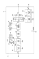
- FIG. 1 is a schematic diagram of a vehicle equipped with an engine ignition device.
- FIG. 2 is a schematic block diagram of an example of a switch control device.
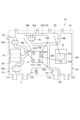
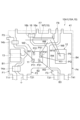
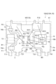
- FIG. 3 is a plan view showing an example of the layout of the internal configuration of an igniter.
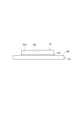
- FIG. 4 is a diagram for explaining the layout relationship between the lead frame and the switch element.
- FIG. 5 is a schematic diagram for explaining the reason why a switch element malfunctions.
- FIG. 6 is a schematic diagram showing the relationship between the gate signal, the emitter voltage, and the gate-emitter voltage in the igniter shown in FIG.
- FIG. 7 is a diagram showing a modified example of the connection of the capacitor provided in the igniter.
- FIG. 8 is a plan view showing a first example of the layout of the internal configuration of the igniter according to the modified example shown in FIG.
- FIG. 9 is a plan view showing a second example of the layout of the internal configuration of the igniter according to the modified example shown in FIG.
- FIG. 10 is a diagram for explaining the positional relationship between the switch elements and the capacitors.
- FIG. 11 is a diagram showing an example of the configuration of a vehicle.
- FIG. 1 is a schematic diagram of a vehicle equipped with an engine ignition device. Specifically, FIG. 1 is a diagram showing a mechanism for driving a gasoline engine in vehicle X. Although omitted in FIG. 1, vehicle X also has components other than those shown in FIG. 1.
- vehicle X has an engine ignition device 1, a power source 2, and an engine control unit (external control device) 3 as mechanisms for driving a gasoline engine.
- power source 2 is a car battery.
- engine control unit 3 will be referred to as ECU (Engine control unit) 3.
- the engine ignition device 1 operates by receiving power from a power source 2.
- the engine ignition device 1 is a device for igniting fuel in a gasoline engine in response to an ignition command signal IGT from an ECU 3.
- the ignition command signal IGT corresponds to a control signal from the ECU 3, which is an external control device.
- the fuel is a mixture of gasoline and air.
- the engine ignition device 1 includes an igniter 10, an ignition coil 4, and a spark plug 5.
- the ignition coil 4 includes a primary coil 4a and a secondary coil 4b.
- the first terminals of the primary coil 4a and the secondary coil 4b are electrically connected to the power source 2.
- the second terminal of the primary coil 4a is electrically connected to the output terminal T4 of the igniter 10.
- the second terminal of the secondary coil 4b is electrically connected to the spark plug 5.
- the igniter 10 has a switch control device 11 and a switch element 12.
- the igniter 10 controls the on/off of the switch element 12 based on an ignition instruction signal IGT supplied from the ECU 3.
- the switch element 12 When the switch element 12 is turned on based on the ignition command signal IGT, the battery voltage VBAT is applied from the power source 2 to the primary coil 4a of the ignition coil 4, and the current I1 flowing through the primary coil 4a increases over time.
- the switch element 12 When the switch element 12 is turned off based on the ignition command signal IGT, the current I1 in the primary coil 4a is cut off. At this time, a primary voltage proportional to the time derivative of the current I1 is generated in the primary coil 4a.
- a secondary voltage equal to the primary voltage multiplied by the winding ratio is generated in the secondary coil 4b. The secondary voltage generated in this way causes a spark in the spark plug 5.
- the igniter 10 has a high-potential power supply terminal T1 to which a battery voltage VBAT is supplied from the power supply 2, and an output terminal T4 electrically connected to the primary coil 4a of the ignition coil 4.
- the igniter 10 has a signal input terminal T3 electrically connected to the ECU 3, and a ground terminal T2 connected to ground.
- An ignition command signal IGT is input from the ECU 3 to the signal input terminal T3.
- the igniter 10 includes a switch control device 11, a switch element 12, a resistor 13, a capacitor 14a, a capacitor 14b, a shunt resistor 15, and a capacitor 16.
- the igniter 10 is modularized and housed in a single package.
- the switch element 12 is configured as a single semiconductor chip including a transistor 121.
- the transistor 121 is an IGBT (Insulated Gate Bipolar Transistor).
- Each terminal (C, G, E) of the transistor 121 may be described as a semiconductor chip, that is, a terminal of the switch element 12.
- the first terminal of resistor 13 is electrically connected to the high potential side power supply terminal T1.
- the second terminal of resistor 13 is electrically connected to the high potential side power supply terminal P1 of the switch control device 11.
- Resistor 13 reduces, for example, a surge voltage superimposed on the battery voltage VBAT, and relieves stress on the switch control device 11.
- the battery voltage VBAT is supplied to the switch control device 11 via resistor 13 as the high potential side power supply voltage VDD.
- Capacitor 14a is electrically connected between the high-potential side power supply terminal T1 and the ground terminal T2. Capacitor 14a, for example, reduces noise (e.g., spike noise) superimposed on the battery voltage VBAT and stabilizes the high-potential side power supply voltage VDD.
- noise e.g., spike noise
- Capacitor 14b is electrically connected between the second terminal of resistor 13 and ground terminal T2. Capacitor 14b functions, for example, as a bypass capacitor that stabilizes the high-potential power supply voltage VDD.
- the switch control device 11 has a high-potential power supply terminal P1 electrically connected to the second terminal of the resistor 13 and to which the high-potential power supply voltage VDD is input, and a ground terminal P2 electrically connected to the ground terminal T2.
- the wiring that transmits the high-potential power supply voltage VDD from the high-potential power supply terminal P1 is referred to as the first voltage wiring L1
- the wiring that transmits the ground voltage (low-potential voltage) AGND from the ground terminal P2 is referred to as the ground wiring L2.
- the switch control device 11 has a signal input terminal P3 electrically connected to the signal input terminal T3 to which the ignition command signal IGT is input, an output terminal P4 electrically connected to the switch element 12, and an input terminal P5 to which the current flowing from the switch element 12 to the shunt resistor 15 is input.
- the switch control device 11 has a reference voltage source 21, a regulator 22, a low voltage protection circuit (BUVP: Battery Under Voltage Protection) 23, an over voltage protection circuit (BOVP: Battery Over Voltage Protection) 24, a signal detection circuit 25, a delay circuit 26, an overcurrent protection circuit 27, a drive circuit 28, and a current detection circuit 29.
- BUVP Battery Under Voltage Protection
- BOVP Battery Over Voltage Protection
- the reference voltage source 21 generates a reference voltage Vref that serves as a basis for voltage comparison in the switch control device 11.
- the wiring that transmits the reference voltage Vref generated by the reference voltage source 21 is called the second voltage wiring L3.
- the reference voltage source 21 is connected between the second voltage wiring L3 and the ground wiring L2.
- the reference voltage source 21 is, for example, a bandgap reference circuit.
- the regulator 22 generates a drive voltage Vdd stabilized to a predetermined level based on the reference voltage Vref and the high-potential power supply voltage VDD.
- the wiring through which the drive voltage Vdd is transmitted is referred to as the fourth voltage wiring L4.
- the low-voltage protection circuit 23 compares the high-potential side power supply voltage VDD with a predetermined threshold voltage, and outputs a detection signal K1 whose level corresponds to the comparison result.
- the threshold voltage of the low-voltage protection circuit 23 is set according to, for example, the lower limit voltage of the voltage range in which the switch control device 11 can operate.
- the overvoltage protection circuit 24 compares the high-potential side power supply voltage VDD with a predetermined threshold voltage, and outputs a detection signal K2 whose level corresponds to the comparison result.
- the threshold voltage of the overvoltage protection circuit 24 is set according to, for example, the upper limit voltage of the voltage range in which the switch control device 11 can operate.
- the signal detection circuit 25 detects the ignition command signal IGT from the ECU 3 and outputs a received signal S1.
- the delay circuit 26 gives a predetermined delay to the received signal S1.
- the predetermined delay is set so that the time difference (delay) between the transition of the ignition command signal IGT and the discharge of the spark plug 5 is a predetermined value.
- the overcurrent protection circuit 27 generates a control signal S3 to be supplied to the drive circuit 28 based on the output S2 from the delay circuit 26, the detection signal K1 from the low voltage protection circuit 23, and the detection signal K2 from the overvoltage protection circuit 24.
- the overcurrent protection circuit 27 generates the control signal S3 based on the output S2 so that the switch element 12 is not turned on for a predetermined current protection time.
- the drive circuit 28 outputs a gate signal Sg that turns the switch element 12 on and off based on the control signal S3 and the detection signal CE from the current detection circuit 29.
- the current detection circuit 29 detects the emitter current Ie flowing from the emitter terminal (second main terminal) E of the switch element 12 to the shunt resistor 15. Since the emitter current Ie corresponds to the collector current Ic flowing through the switch element 12, the detection result of the emitter current Ie represents the state of the collector current Ic.
- the current detection circuit 29 generates a detection signal CE according to the detection result of the emitter current Ie.
- the detection signal CE is input to the drive circuit 28.
- the drive circuit 28 lowers the voltage level of the gate signal Sg based on the detection signal CE. For example, the drive circuit 28 lowers the voltage level of the gate signal Sg by adjusting the impedance on the switch element 12 side as viewed from the drive circuit 28 in response to the detection signal CE. This limits the collector current Ic to an upper limit value or less. Therefore, the current detection circuit 29 also functions as an overcurrent protection circuit.
- FIG. 2 is a schematic block diagram of an example of the switch control device 11. An example of the signal detection circuit 25, the drive circuit 28, and the current detection circuit 29 will be described using FIG. 2.
- An example of the signal detection circuit 25 has a filter circuit 251 and a comparison circuit 252.
- the filter circuit 251 receives the ignition instruction signal IGT from the signal input terminal P3.
- the filter circuit 251 is a circuit for removing noise superimposed on the ignition instruction signal IGT.
- the filter circuit 251 is, for example, an RC filter circuit composed of a resistor and a capacitor.
- the comparison circuit 252 receives the output from the filter circuit 251 (the ignition instruction signal IGT from which noise has been removed) and a reference voltage Vref.
- the comparison circuit 252 compares the output from the filter circuit 251 with the reference voltage Vref to generate a received signal S1.
- An example of the drive circuit 28 has transistors 281 and 282 connected in series between the fourth voltage wiring L4 and the ground wiring L2.
- the transistor 281 is, for example, a PMOSFET (P-channel Metal Oxide Semiconductor Field Effect Transistor), and the transistor 282 is, for example, an NMOSFET (N-channel MOSFET).
- a resistor 283 is disposed between the transistor 281 and a node N2 between the transistors 281 and 282.
- a resistor 284 is disposed between the transistor 282 and the node N2.
- the node N2 is electrically connected to the output terminal P4.
- the drive circuit 28 generates the gate signal Sg by adjusting the voltage level of the signal obtained by turning on and off the transistors 281 and 282 in response to the control signal S3 from the overcurrent protection circuit 27 as necessary based on the detection signal CE described above.
- the drive circuit 28 has transistors 281, 282 and resistors 283, 284 connected in series, the effect of noise coming from the output terminal P4 can be reduced by lowering the on-resistance of the transistors 281, 282 and the resistance of the resistors 283, 284.
- An example of the current detection circuit 29 has a filter circuit 291 and a comparison circuit 292.
- the filter circuit 291 receives the emitter current Ie from the input terminal P5.
- the filter circuit 291 is a circuit for removing noise superimposed on the emitter current Ie.
- the filter circuit 291 is, for example, an RC filter circuit composed of a resistor and a capacitor.
- the comparison circuit 292 receives the output from the filter circuit 291 (a voltage corresponding to the emitter current Ie from which noise has been removed) and a reference voltage Vref.
- the comparison circuit 292 compares the output from the filter circuit 291 with the reference voltage Vref to generate a detection signal CE.
- the switch element 12 includes a transistor 121.
- the collector terminal C of the switch element 12 is electrically connected to the output terminal T4.
- the collector terminal (first main terminal) C is electrically connected to the primary coil 4a of the ignition coil 4.
- the emitter terminal (second main terminal) E of the switch element 12 is electrically connected to the ground terminal T2 via a shunt resistor 15.
- the gate terminal G of the switch element 12 is electrically connected to the output terminal P4.
- a gate signal Sg is input to the gate terminal G.
- the switch element 12 may have a first protection element provided between the gate and collector of the transistor 121 for the purpose of overvoltage protection.
- the first protection element includes, for example, a diode connected in reverse series between the gate and collector of the transistor 121.
- the diode is, for example, a Zener diode.
- the first protection element clamps the overvoltage (e.g., surge noise, etc.) between the gate and collector to a predetermined voltage.
- the switch element 12 may have a second protection element provided between the gate and emitter of the transistor 121 for the purpose of overvoltage protection.
- the second protection element includes, for example, a diode connected in reverse series between the gate and emitter of the transistor 121.
- the diode is, for example, a Zener diode.
- the second protection element clamps the overvoltage (e.g., surge noise, etc.) between the gate and emitter to a predetermined voltage.
- the first terminal 15a of the shunt resistor 15 is electrically connected to the emitter terminal E, and the second terminal 15b of the shunt resistor 15 is electrically connected to the ground terminal T2.
- the shunt resistor 15 is a resistor for detecting the state of the emitter current Ie (the collector current Ic of the switch element 12).
- the resistance value of the shunt resistor 15 is several m ⁇ to several tens of m ⁇ , for example, 5 m ⁇ .
- the mounting portion B2 of the lead frame F2 is connected to the lead frame F6 by a wire W7.
- the wire W7 is positioned opposite the lead portion T21 with respect to the switch control device 11.
- FIG. 5 is a schematic diagram for explaining the reason why the switch element 12 malfunctions.
- the wavy line indicates the modulation due to noise.
- the voltage level of the gate-emitter voltage Vge may drop from the desired level, as shown in the voltage level between time t1a and time t2 in FIG. 5, and even if the gate signal Sg is at a low level, the voltage level of the gate-emitter voltage Vge may increase from the desired level, as shown in the voltage level between time t2a and time t2b in FIG. 5.
- FIG. 6 is a schematic diagram showing the relationship between the gate signal Sg, the emitter voltage Ve, and the gate-emitter voltage Vge when the igniter 10 equipped with the capacitor 16 is operating.
- the logic level of the gate signal Sg is high between time t1 and time t2, and the logic level transitions to low at time t2.
- the switch element 12 When the gate signal Sg is high, the switch element 12 corresponds to the on state, and when the gate signal Sg is low, the switch element 12 corresponds to the off state.
- the dashed line shown in FIG. 6 indicates the noise level in the case of FIG. 5.
- a desired level according to the logic level of the gate signal Sg can be achieved as the voltage level of the gate-emitter voltage Vge. As a result, malfunction of the switch element 12 can be prevented.
- the igniter 10 when the igniter 10 includes the resistor 13 and the capacitors 14a and 14b, the circuit formed by the resistor 13 and the capacitors 14a and 14b functions as a high-frequency filter. Therefore, the resistor 13 and the capacitors 14a and 14b can mitigate the effects of noise injected from the power supply 2 via the high-potential power supply terminal T1. As a result, malfunction of the switch element 12 can be further prevented.
- the signal detection circuit 25 has a filter circuit 251
- the noise contained in the ignition instruction signal IGT can be reduced.
- the igniter 10 has a delay circuit 26
- the effect of the noise contained in the ignition instruction signal IGT can be further reduced. As a result, malfunction of the switch element 12 can be further prevented.
- the capacitor 16 is connected in parallel to the shunt resistor 15 between the emitter terminal E and the ground terminal T2.
- Fig. 1 as an example of the connection form of the capacitor 16, a case where the first terminal 16a of the capacitor 16 is connected to the node N1 or is connected closer to the shunt resistor 15 than the node N1 has been described.
- the first terminal 16a of the capacitor 16 may be connected closer to the emitter terminal E than the node N1, as shown in FIG. 7.
- the igniter 10 shown in FIG. 7 may also be referred to as igniter 10A.
- the first terminal 16a of the capacitor 16 is connected closer to the emitter terminal E than the node N1, so the electrical length between the emitter terminal E and the first terminal 16a is short. This makes it possible to reduce the effects of the inductance component contained in the wiring L5 between the emitter terminal E and the shunt resistor 15. As a result, the effects of noise can be further reduced. Because the first terminal 16a is connected closer to the emitter terminal E than the node N1, the noise superimposed on the emitter current Ie input to the current detection circuit 29 via the input terminal P5 can also be reduced.
- Fig. 8 is a plan view showing an example of the layout of the internal structure of the igniter 10A.
- the sealing resin 41 is indicated by a two-dot chain line.
- the igniter 10A (10) shown in Fig. 8 may be referred to as an igniter 10A1.
- the same reference numerals are used to designate the same elements as in the layout example of the igniter 10 shown in Fig. 3, and duplicate explanations will be omitted as appropriate.
- the igniter 10A1 includes a sealing resin 41 that seals a portion of the lead frame and the components of the igniter 10A1, and a plurality of lead frames F1, F2 (first lead frame), F3, and F4 (second lead frame) that protrude from the sealing resin 41.
- the sealing resin 41 is formed in a roughly rectangular parallelepiped shape. Each of the lead frames F1 to F4 protrudes from one side of the sealing resin 41. In FIG. 8, the sealing resin 41 is indicated by a two-dot chain line.
- the igniter 10A1 has lead frames F5, F7, and F8 that are fitted inside sealing resin 41.
- Each of the lead frames F1 to F5, F7, and F8 can be made of a conductive metal, such as copper (Cu), a Cu alloy, nickel (Ni), a Ni alloy, or a 42 alloy.
- the lead frames F1 to F5, F7, and F8 may be plated with Pd plating, Ag plating, or the like.
- the sealing resin 41 can be made of an insulating resin, such as epoxy resin.
- the lead frames F1 to F4 have mounting portions B1 to B4 and lead portions T11, T21, T31, and T41 extending from the mounting portions B1 to B4.
- the lead portions T11, T21, T31, and T41 correspond to the respective terminals of the igniter 10 shown in FIG. 1.
- the specific correspondence is the same as in the layout example of the igniter 10 shown in FIG. 3.
- a resistor 13 is connected between the mounting portion B1 of the lead frame F1 and the lead frame F5.
- a capacitor 14a is connected between the mounting portion B1 of the lead frame F1 and the mounting portion B2 of the lead frame F2.
- a capacitor 14b is connected between the mounting portion B2 of the lead frame F2 and the lead frame F5.
- a switch control device 11 is mounted on mounting portion B2 of lead frame F2.
- a switch element 12 is mounted on mounting portion B4 of lead frame F4.
- a gate pad PG and an emitter pad PE are exposed on the top surface of the switch element 12.
- the gate pad PG and the emitter pad PE correspond to the gate terminal G and the emitter terminal E shown in FIG. 1.
- Pads P11, P21, P31, P41, and P51 corresponding to each terminal shown in FIG. 1 are exposed on the top surface of the switch control device 11.
- the specific correspondence between the pads P11, P21, P31, P41, and P51 and each terminal shown in FIG. 1 is the same as in the layout example of the igniter 10 shown in FIG. 3.
- the pad P11 is connected to a lead frame F5 by a wire W1.
- the pad P21 is connected to the mounting portion B2 of the lead frame F2 by a wire W2.
- the pad P31 is connected to the mounting portion B3 of the lead frame F3 by a wire W3.
- the pad P41 is connected to the gate pad PG of the switch element 12 by a wire W4.
- the pad P51 is connected to a lead frame F8 by a wire W8.
- the emitter pad PE of the switch element 12 is connected to the lead frame F7 via a wire W9.
- the emitter pad PE is also connected to the lead frame F8 via a wire W10.
- the mounting portion B2 of the lead frame F2 is connected to the lead frame F8 via a wire W7.
- the wire W7 is disposed on the opposite side of the switch control device 11 from the lead portion T21.
- Wires W1, W2, W3, W4, W8, W9, and W10 are, for example, aluminum wires with a diameter of, for example, 125 ⁇ m.
- Wire W7 is, for example, aluminum wire with a diameter of, for example, 250 ⁇ m.
- the resistance value of wire W7 is several m ⁇ to several tens of m ⁇ , for example, 5 m ⁇ .
- the resistance component of this wire W7 functions as the shunt resistor 15 shown in FIG. 1, similar to the layout example of the igniter 10 shown in FIG. 3.
- a capacitor 16 is connected between the mounting portion B2 of the lead frame F2 and the lead frame F7.
- the capacitor 16 is connected to the mounting portion B2 and the lead frame F7 by Ag paste, solder, or the like.
- the capacitor 16 is disposed opposite the switch control device 11 with respect to the wire W7.
- the capacitor 16 is disposed parallel to the wire W7.
- the emitter pad PE is connected to the lead frame F2 via the wire W10, the lead frame F8, and the wire W7.
- the lead frame F2 has a lead portion T21 corresponding to the ground terminal T2, so the emitter pad PE is electrically connected to the ground terminal T2 via the wire W7 (shunt resistor 15).
- the lead frame F8 is connected to the pad P51 via the wire W8, so the lead frame F8 corresponds to the node N1 shown in FIG. 1.
- the capacitor 16 is connected between the mounting portion B2 of the lead frame F2 and the lead frame F7, and the lead frame F7 is connected to the emitter pad PE via the wire W9. Therefore, in the first layout example of the igniter 10A1 (10A, 10) shown in FIG. 8, the first terminal 16a of the capacitor 16 is electrically connected closer to the emitter pad PE (emitter terminal E) than the node N1.
- Fig. 9 is a plan view showing a second layout example of the internal configuration of the igniter 10A.
- the sealing resin 41 is indicated by a two-dot chain line.
- the igniter 10A (10) shown in Fig. 9 may be referred to as an igniter 10A2.
- the same elements as those in the layout example shown in Fig. 3 are given the same reference numerals, and duplicate explanations will be omitted as appropriate.
- the igniter 10A2 includes a sealing resin 41 that seals a portion of the lead frame and the components of the igniter 10A2, and a plurality of lead frames F1, F2 (first lead frame), F3, and F4 (second lead frame) that protrude from the sealing resin 41.
- the sealing resin 41 is formed in a roughly rectangular parallelepiped shape. Each of the lead frames F1 to F4 protrudes from one side of the sealing resin 41.
- the igniter 10A2 has a lead frame F5 and a lead frame (third lead frame) F10 that are housed in a sealing resin 41.
- Each of the lead frames F1 to F5, F10 can be made of a conductive metal, such as copper (Cu), a Cu alloy, nickel (Ni), a Ni alloy, or a 42 alloy.
- the lead frames F1 to F5, F10 may be plated with Pd, Ag, or the like.
- the lead frames F1 to F4 have mounting portions B1 to B4 and lead portions T11, T21, T31, and T41 extending from the mounting portions B1 to B4.
- the lead portions T11, T21, T31, and T41 correspond to the respective terminals of the igniter 10 shown in FIG. 1.
- the specific correspondence is the same as in the layout example shown in FIG. 3.
- a resistor 13 is connected between the mounting portion B1 of the lead frame F1 and the lead frame F5.
- a capacitor 14a is connected between the mounting portion B1 of the lead frame F1 and the mounting portion B2 of the lead frame F2.
- a capacitor 14b is connected between the mounting portion B2 of the lead frame F2 and the lead frame F5.
- a switch control device 11 is mounted on mounting portion B2 of lead frame F2.
- a switch element 12 is mounted on mounting portion B4 of lead frame F4.
- a gate pad PG and an emitter pad PE are exposed on the top surface of the switch element 12.
- the gate pad PG and the emitter pad PE correspond to the gate terminal G and the emitter terminal E shown in FIG. 1.
- Pads P11, P21, P31, P41, and P51 corresponding to each terminal shown in FIG. 1 are exposed on the top surface of the switch control device 11.
- the specific correspondence between the pads P11, P21, P31, P41, and P51 and each terminal shown in FIG. 1 is the same as in the layout example shown in FIG. 3.
- the pad P11 is connected to a lead frame F5 by a wire W1.
- the pad P21 is connected to the mounting portion B2 of the lead frame F2 by a wire W2.
- the pad P31 is connected to the mounting portion B3 of the lead frame F3 by a wire W3.
- the pad P41 is connected to the gate pad PG of the switch element 12 by a wire W4.
- the pad P51 is connected to the lead frame F10 by a wire W11.
- the emitter pad PE of the switch element 12 is connected to a lead frame F10 by a wire W12.
- the mounting portion B2 of the lead frame F2 is connected to the lead frame F10 via a wire W7.
- the wire W7 is positioned opposite the lead portion T21 with respect to the switch control device 11.
- the capacitor 16 is disposed on the emitter pad PE as shown in Figures 9 and 10.
- Figure 10 is a schematic diagram for explaining the positional relationship of the capacitor 16 with respect to the switch element 12.
- Figure 10 also shows lead frames F2, F4 and wire W13.
- the capacitor 16 is fixed to the emitter pad PE with Ag paste, solder, or the like.
- the surface of the capacitor 16 that is fixed to the emitter pad PE corresponds to the first terminal 16a, and the surface opposite the emitter pad PE corresponds to the second terminal 16b.
- the second terminal 16b of the capacitor 16 is connected to the mounting portion B2 of the lead frame F2 by a wire W13.
- the wire W13 is, for example, an aluminum wire and has a diameter of, for example, 125 ⁇ m.
- FIG. 11 is a diagram showing an example of the configuration of a vehicle on which the engine ignition device 1 according to the embodiment is mounted.
- Vehicle X includes the power source 2 and ECU 3 described above, an engine unit 51 with a generator, a high-power DC/DC converter 52, an inverter 53, a motor 54, a drive unit 55, a high-voltage battery 56, and a DC/DC converter 57.
- the mounting positions of each component in FIG. 11 differ from the actual positions.
- Vehicle X shown in FIG. 11 is a so-called series hybrid vehicle.
- the generator-equipped engine section 51 includes a generator, an engine dedicated to generating electricity to rotate the generator, and the engine ignition device 1 according to the various embodiments described above. Because the energy conversion efficiency of the engine varies greatly depending on the timing of ignition, the ignition timing must be controlled by the ECU 3 in consideration of the rotation angle of the crank that converts the reciprocating motion of the piston in the cylinder into rotational motion and the required amount of electricity generation. For this reason, the engine ignition device 1 according to the embodiment is provided for each cylinder of the engine.
- the high-power DC/DC converter 52 converts the DC power generated by the generator of the generator-equipped engine section 51 into high-voltage DC power.
- the high-power DC/DC converter 52 supplies the high-voltage DC power to the inverter 53 and the high-voltage battery 56.
- the high-power DC/DC converter 52 can supply the discharge power discharged from the high-voltage battery 56 to the inverter 53.
- the high-power DC/DC converter 52 can also charge the high-voltage battery 56 with regenerative power supplied from the inverter 53 when the vehicle X decelerates.
- the inverter 53 receives DC power from the high-power DC/DC converter 52 and converts the received DC power into three-phase AC power.
- the motor 54 has a shaft and rotates the shaft using three-phase AC power supplied from the inverter 53.
- the drive unit 55 transmits the power generated by the rotation of the shaft of the motor 54 to the drive wheels of the vehicle X.
- the rear wheels of the vehicle X are the drive wheels, but the drive wheels are not limited to the rear wheels.
- the front wheels may be the drive wheels, or both the front and rear wheels may be the drive wheels.
- the DC/DC converter 57 receives DC power from the high-power DC/DC converter 52 and converts the received DC power into low-voltage DC power.
- the power source 2 which is a low-voltage battery, is charged by the low-voltage DC power output from the DC/DC converter 57.
- the discharge power discharged from the power source 2 is supplied to the engine ignition device 1 according to the embodiment, etc.
- the vehicle in which the engine ignition device 1 according to the embodiment is mounted is not limited to a hybrid vehicle such as vehicle X shown in FIG. 11, but may be any vehicle equipped with an engine.
- MOSFET Metal-Oxide-Semiconductor Field-Effect Transistor
- the load control device, igniter, engine ignition device, and vehicle described in the above embodiment and modified examples can reduce the effects of noise injected from the load to be controlled.
- FIG. 1 a switch element (12) having a first main terminal (G) connected to a load (4), and having a second main terminal (E) and a control terminal (G); a shunt resistor (15) electrically connected between the second main terminal and a ground terminal (T2) for detecting a current flowing through the switch element; a switch control device (11) configured to output a drive signal (Sg) for driving the switch element to the control terminal based on a detection signal (CE) based on a detection result of the shunt resistor and a control signal (IGT) from an external control device (3); a capacitor (16) electrically connected in parallel with the shunt resistor between the second main terminal and the ground terminal; Equipped with A load control device (10).
- the switch control device (11) an input terminal (P5) connected to a wiring (L5) connecting the second main terminal and the shunt resistor, and receiving an input of a current flowing from the second main terminal to the shunt resistor; a current detection circuit (29) configured to detect a current input to the input terminal as a current flowing through the switch element and output a detection signal; a drive circuit (28) configured to generate the drive signal based on the detection signal output from the current detection circuit and the control signal; Equipped with The capacitor has a first terminal (16a) electrically connected to the second main terminal and a second terminal (16b) electrically connected to the ground terminal, The first terminal is electrically connected to the wiring (L5) closer to the shunt resistor than a node (N1) between the wiring and the input terminal or to the node. 2.
- the switch control device (11) an input terminal (P5) connected to a wiring (L5) connecting the second main terminal and the shunt resistor, and receiving an input of a current flowing from the second main terminal to the shunt resistor; a current detection circuit (29) configured to detect a current input to the input terminal as a current flowing through the switch element and output a detection signal; a drive circuit (28) configured to generate the drive signal based on the detection signal output from the current detection circuit and the control signal; Equipped with The capacitor (16) has a first terminal (16a) electrically connected to the second main terminal (E) and a second terminal (16b) electrically connected to the ground terminal, The first terminal is electrically connected to the wiring (L5) closer to the second main terminal than a node (N1) between the wiring and the input terminal. 2.
- FIG. 8 (First layout example of components of an igniter according to a modified example, FIG. 8) a first lead frame (F2) on which the switch control device is mounted and which is electrically connected to ground; a second lead frame (F4) on which the switch element is mounted; A third lead frame (F8); A fourth lead frame (F7); having The switch control device has an input terminal (corresponding to a pad P51 in FIG. 8 ) to which a current flowing from the second main terminal to the shunt resistor is input, In the switch element, the first main terminal (corresponding to the collector electrode PC shown in FIG. 4) is located opposite to the second main terminal (corresponding to the emitter pad PE in FIG.
- the switch element is mounted on the second lead frame by the first main terminal being fixed to the second lead frame,
- the first lead frame (F2) and the fourth lead frame (F7) are connected by the capacitor (16);
- the first lead frame (F2) and the third lead frame (F8) are connected by the shunt resistor (W7),
- the third lead frame (F8) and the second main terminal are connected by a wire (W10),
- the fourth lead frame (F7) and the second main terminal are connected by a wire (W9),
- the input terminal (P51) of the switch control device is connected to the third lead frame by a wire (W8). 4.
- the load control device according to claim 1 or 3.
- FIGS. 9 and 10 (Second layout example of components of igniter according to modified example, FIGS. 9 and 10) a first lead frame (F2) on which the switch control device (11) is mounted and which is electrically connected to ground; a second lead frame (F4) on which the switch element (12) is mounted; A third lead frame (F10); having The switch control device has an input terminal (corresponding to a pad P51 in FIG. 9 ) to which a current flowing from the second main terminal to the shunt resistor is input, In the switch element, the first main terminal (corresponding to the collector electrode PC shown in FIG. 10 ) is located opposite to the second main terminal (corresponding to the emitter pad PE in FIGS.
- the switch element (12) is mounted on the second lead frame by the first main terminal being fixed to the second lead frame,
- the first lead frame (F2) and the third lead frame (F10) are connected by the shunt resistor (W7)
- the capacitor (16) is mounted on the second main terminal (corresponding to the emitter pad PE in FIGS. 9 and 10 ) by fixing a first terminal (16 a) of the capacitor to the second main terminal,
- a second terminal (16b) located opposite to the first terminal (16a) is connected to the first lead frame (F2) by a wire (W13);
- the third lead frame (F10) and the second main terminal pad are connected by a wire (W12);
- the input terminal (corresponding to pad P51 in FIG. 9) of the switch control device (11) is connected to the third lead frame (F10) by a wire (W11). 4.
- the load control device (10) according to any one of appendices 1 to 5 is provided,
- the load is an ignition coil (4),
- the first main terminal is connected to a primary coil (4a) of the ignition coil,
- the control signal is an ignition command signal (IGT). Igniter.
- FIG. 1 An ignition coil (4); An igniter (10) according to appendix 6 connected to a primary coil (4a) of the ignition coil; a spark plug (5) connected to the secondary coil (4b) of the ignition coil; Equipped with Engine ignition device (1).
- Appendix 8 (Vehicle shown in FIG. 11) An engine ignition device (1) according to appendix 7, A power source (2) for supplying power to the engine ignition device; an engine control unit (3) configured to control the engine ignition device; Equipped with vehicle.
- the switch control device (11) an input terminal (P5) connected to a wiring (L5) connecting the second main terminal and the shunt resistor, and receiving an input of a current flowing from the second main terminal to the shunt resistor; a current detection circuit (29) configured to detect a current input to the input terminal as a current flowing through the switch element and output a detection signal; a drive circuit (28) configured to generate the drive signal based on the detection signal output from the current detection circuit and the control signal; Equipped with 2.
Landscapes
- Engineering & Computer Science (AREA)
- Chemical & Material Sciences (AREA)
- Combustion & Propulsion (AREA)
- Mechanical Engineering (AREA)
- General Engineering & Computer Science (AREA)
- Ignition Installations For Internal Combustion Engines (AREA)
Abstract
一実施形態に係る負荷制御装置は、負荷に接続される第1主端子、第2主端子及び制御端子を有するスイッチ素子と、第2主端子とグランド端子との間に電気的に接続されており、スイッチ素子に流れる電流を検出するためのシャント抵抗と、シャント抵抗の検出結果に基づいた検出信号と外部制御装置からの制御信号に基づいて、スイッチ素子を駆動する駆動信号を制御端子に出力するように構成されたスイッチ制御装置と、第2主端子とグランド端子との間にシャント抵抗と並列に電気的に接続されるコンデンサと、を備える。
Description
本発明は、負荷制御装置、イグナイタ、エンジン点火装置及び車両に関する。
従来、スイッチ素子及びスイッチ制御回路を含む装置の一例は、イグナイタである。イグナイタにおいて、上記スイッチ素子はイグニッションコイルの一次コイルに接続されている。イグナイタが備えるスイッチ制御回路は、上記スイッチ素子を点火信号に応じて制御する。このようなスイッチ素子の制御によって、イグナイタはイグニッションコイルを制御する(特許文献1参照)。
[概要]
イグナイタにおいて、スイッチ素子はイグニッションコイルの一次コイルに接続されている。そのため、スイッチ素子を動作させることでイグニッションコイルを制御している場合、一次コイル側からスイッチ素子に向けてノイズが注入され、そのノイズによってスイッチ制御回路が誤動作する可能性があった。
イグナイタにおいて、スイッチ素子はイグニッションコイルの一次コイルに接続されている。そのため、スイッチ素子を動作させることでイグニッションコイルを制御している場合、一次コイル側からスイッチ素子に向けてノイズが注入され、そのノイズによってスイッチ制御回路が誤動作する可能性があった。
本開示の一側面の目的は、制御すべき負荷側から注入されるノイズの影響を低減可能な負荷制御装置、イグナイタ、エンジン点火装置及び車両を提供することである。
本開示に係る負荷制御装置は、負荷に接続される第1主端子、第2主端子及び制御端子を有するスイッチ素子と、前記第2主端子とグランド端子との間に接続されており、前記スイッチ素子に流れる電流を検出するためのシャント抵抗と、前記シャント抵抗の検出結果に基づいた検出信号と外部制御装置からの制御信号に基づいて、前記スイッチ素子を駆動する駆動信号を前記制御端子に出力するスイッチ制御装置と、前記第2主端子と前記グランド端子との間に前記シャント抵抗と並列に接続されるコンデンサと、を備える。
[詳細な説明]
図面を参照しながら本開示の実施形態を説明する。図面の説明においては同一要素には同一符号を付し、重複する説明を省略する。
図面を参照しながら本開示の実施形態を説明する。図面の説明においては同一要素には同一符号を付し、重複する説明を省略する。
図1は、エンジン点火装置を備えた車両の模式図である。具体的には、図1は、車両Xにおいて、ガソリンエンジンを駆動する機構を示した図面である。図1では省略しているが、車両Xは、図1に示した構成以外の構成も備える。
図1に示したように、車両Xは、ガソリンエンジンを駆動する機構として、エンジン点火装置1と、電源2と、エンジンコントロールユニット(外部制御装置)3と、を有する。以下の説明において、電源2はカーバッテリである。以下では、エンジンコントロールユニット3をECU(Engine control unit)3と称す。
エンジン点火装置1は、電源2からの電力供給を受けて動作する。エンジン点火装置1は、ECU3からの点火指示信号IGTに応じて、ガソリンエンジン内の燃料に点火するための装置である。点火指示信号IGTは、外部制御装置であるECU3からの制御信号に相当する。上記燃料は、ガソリンと空気の混合気である。エンジン点火装置1は、イグナイタ10、イグニッションコイル4及び点火プラグ5を備える。
イグニッションコイル4は、一次コイル4aおよび二次コイル4bを備えている。一次コイル4a及び二次コイル4bの第1端子は電源2に電気的に接続されている。一次コイル4aの第2端子はイグナイタ10の出力端子T4に電気的に接続されている。二次コイル4bの第2端子は点火プラグ5に電気的に接続されている。
イグナイタ10は、スイッチ制御装置11とスイッチ素子12を有する。イグナイタ10は、ECU3から供給される点火指示信号IGTに基づいて、スイッチ素子12をオンオフ制御する。
点火指示信号IGTに基づいてスイッチ素子12がオンすると、イグニッションコイル4の一次コイル4aに電源2からバッテリ電圧VBATが印加され、一次コイル4aに流れる電流I1が時間とともに増大する。点火指示信号IGTに基づいてスイッチ素子12がオフすると、一次コイル4aの電流I1が遮断される。このとき、一次コイル4aには、電流I1の時間微分に比例した一次電圧が発生する。二次コイル4bには、一次電圧に巻線比を乗じた二次電圧が発生する。このように発生した二次電圧により点火プラグ5にスパーク(火花)を生じさせる。
図1に示すように、イグナイタ10は、電源2からバッテリ電圧VBATが供給される高電位側電源端子T1と、イグニッションコイル4の一次コイル4aに電気的に接続される出力端子T4を有している。イグナイタ10は、ECU3に電気的に接続される信号入力端子T3と、グランドに接続されたグランド端子T2を有している。信号入力端子T3には、ECU3から点火指示信号IGTが入力される。
イグナイタ10は、スイッチ制御装置11、スイッチ素子12、抵抗13、コンデンサ14a、コンデンサ14b、シャント抵抗15及びコンデンサ16を備える。イグナイタ10は、モジュール化されて1つのパッケージに収容されている。スイッチ素子12は、トランジスタ121を含む1つの半導体チップとして構成されている。本例では、トランジスタ121は、IGBT(Insulated Gate Bipolar Transistor)である。トランジスタ121の各端子(C,G,E)を半導体チップ、つまりスイッチ素子12の端子として説明することがある。
抵抗13の第1端子は高電位側電源端子T1に電気的に接続されている。抵抗13の第2端子はスイッチ制御装置11の高電位側電源端子P1に電気的に接続されている。抵抗13は、例えばバッテリ電圧VBATに重畳するサージ電圧を低減し、スイッチ制御装置11に対するストレスを緩和する。バッテリ電圧VBATは、抵抗13を介して高電位側電源電圧VDDとしてスイッチ制御装置11に供給される。
コンデンサ14aは、高電位側電源端子T1とグランド端子T2との間に電気的に接続されている。コンデンサ14aは、例えば、バッテリ電圧VBATに重畳するノイズ(例えば、スパイクノイズ)を低減し、高電位側電源電圧VDDを安定化する。
コンデンサ14bは、抵抗13の第2端子とグランド端子T2との間に電気的に接続されている。コンデンサ14bは、例えば、高電位側電源電圧VDDを安定化するバイパスコンデンサとして機能する。
スイッチ制御装置11は、抵抗13の第2端子に電気的に接続されており高電位側電源電圧VDDが入力される高電位側電源端子P1と、グランド端子T2に電気的に接続されるグランド端子P2を有している。スイッチ制御装置11において、高電位側電源端子P1から高電位側電源電圧VDDを伝達する配線を第1電圧配線L1と称し、グランド端子P2からグランド電圧(低電位側電圧)AGNDが伝達される配線をグランド配線L2と称す。
スイッチ制御装置11は、信号入力端子T3に電気的に接続されており点火指示信号IGTが入力される信号入力端子P3と、スイッチ素子12に電気的に接続される出力端子P4と、スイッチ素子12からシャント抵抗15に流れる電流が入力される入力端子P5を有する。
スイッチ制御装置11は、基準電圧源21、レギュレータ22、低電圧保護回路(BUVP:Battery Under Voltage Protection)23、過電圧保護回路(BOVP:Battery Over Voltage Protection)24、信号検出回路25、遅延回路26、過通電保護回路27、駆動回路28及び電流検出回路29を有している。
基準電圧源21は、スイッチ制御装置11において電圧比較の基準となる基準電圧Vrefを生成する。基準電圧源21で生成された基準電圧Vrefを伝達する配線を第2電圧配線L3と称す。基準電圧源21は、第2電圧配線L3とグランド配線L2の間に接続されている。基準電圧源21は、例えば、バンドギャップリファレンス回路である。
レギュレータ22は、基準電圧Vrefと高電位側電源電圧VDDとに基づいて、所定レベルに安定化された駆動電圧Vddを生成する。駆動電圧Vddが伝達される配線を第4電圧配線L4と称す。
低電圧保護回路23は、高電位側電源電圧VDDと所定のしきい値電圧とを比較し、比較結果に応じたレベルの検出信号K1を出力する。低電圧保護回路23のしきい値電圧は、例えば、スイッチ制御装置11が動作可能な電圧範囲のうちの下限の電圧に応じて設定される。
過電圧保護回路24は、高電位側電源電圧VDDと所定のしきい値電圧とを比較し、比較結果に応じたレベルの検出信号K2を出力する。過電圧保護回路24のしきい値電圧は、例えば、スイッチ制御装置11が動作可能な電圧範囲のうちの上限の電圧に応じて設定される。
信号検出回路25は、ECU3からの点火指示信号IGTを検出し、受信信号S1を出力する。
遅延回路26は、受信信号S1に所定の遅延量を与える。上記所定の遅延量は、点火指示信号IGTの遷移と点火プラグ5の放電の時間の時間差(遅れ)が所定値となるように設定される。
過通電保護回路27は、遅延回路26からの出力S2、低電圧保護回路23の検出信号K1及び過電圧保護回路24の検出信号K2に基づいて、駆動回路28に供給する制御信号S3を生成する。過通電保護回路27は、出力S2に基づいて、スイッチ素子12が所定の通電保護時間にわたりオンしないように、制御信号S3を生成する。
駆動回路28は、制御信号S3及び電流検出回路29からの検出信号CEに基づいて、スイッチ素子12をオンオフするゲート信号Sgを出力する。
電流検出回路29は、スイッチ素子12のエミッタ端子(第2主端子)Eからシャント抵抗15に流れるエミッタ電流Ieを検出する。エミッタ電流Ieは、スイッチ素子12に流れるコレクタ電流Icに対応するため、エミッタ電流Ieの検出結果は、コレクタ電流Icの状態を表している。電流検出回路29は、エミッタ電流Ieの検出結果に応じた検出信号CEを生成する。検出信号CEは、駆動回路28に入力される。駆動回路28は、検出信号CEに基づいてゲート信号Sgの電圧レベルを低下させる。たとえば、駆動回路28は、検出信号CEに応じて、駆動回路28からみてスイッチ素子12側のインピーダンスを調整することでゲート信号Sgの電圧レベルを低下させる。これにより、コレクタ電流Icを上限値以下に制限する。したがって、電流検出回路29は、過電流保護回路としても機能する。
図2は、スイッチ制御装置11の一例の概略ブロック図である。図2を利用して信号検出回路25、駆動回路28及び電流検出回路29の一例を説明する。
信号検出回路25の一例は、フィルタ回路251及び比較回路252を有する。フィルタ回路251には、信号入力端子P3から点火指示信号IGTが入力される。フィルタ回路251は、点火指示信号IGTに重畳されたノイズを除去するための回路である。フィルタ回路251は、たとえば、抵抗とコンデンサとによって構成されるRCフィルタ回路である。比較回路252には、フィルタ回路251からの出力(ノイズが除去された点火指示信号IGT)と、基準電圧Vrefが入力される。比較回路252は、フィルタ回路251からの出力と基準電圧Vrefとを比較して、受信信号S1を生成する。
駆動回路28の一例は、第4電圧配線L4とグランド配線L2との間に直列接続されたトランジスタ281,282を有している。トランジスタ281は例えばPMOSFET(P-channel Metal Oxide Semiconductor Field Effect Transistor)であり、トランジスタ282は例えばNMOSFET(N-channel MOSFET)である。トランジスタ281とトランジスタ282の間のノードN2とトランジスタ281との間には抵抗283が配置されている。トランジスタ282とノードN2の間には抵抗284が配置されている。ノードN2は出力端子P4に電気的に接続されている。駆動回路28は、トランジスタ281及びトランジスタ282を過通電保護回路27からの制御信号S3に応じてオンオフ動作させることによって得られる信号の電圧レベルを、前述した検出信号CEに基づいて必要に応じて調整することによってゲート信号Sgを生成する。
上記のように、駆動回路28が、直列接続されたトランジスタ281,282と抵抗283,284を有する場合、トランジスタ281,282のオン抵抗及び抵抗283,284の抵抗値を下げることによって、出力端子P4から入ってくるノイズの影響を低減できる。
電流検出回路29の一例は、フィルタ回路291及び比較回路292を有する。フィルタ回路291には、入力端子P5からエミッタ電流Ieが入力される。フィルタ回路291は、エミッタ電流Ieに重畳されたノイズを除去するための回路である。フィルタ回路291は、たとえば、抵抗とコンデンサとによって構成されるRCフィルタ回路である。比較回路292には、フィルタ回路291からの出力(ノイズが除去されたエミッタ電流Ieに対応する電圧)と、基準電圧Vrefが入力される。比較回路292は、フィルタ回路291からの出力と基準電圧Vrefとを比較して、検出信号CEを生成する。
図1に戻ってイグナイタ10を更に説明する。スイッチ素子12は、トランジスタ121を含む。スイッチ素子12のコレクタ端子Cは、出力端子T4に電気的に接続されている。これによって、コレクタ端子(第1主端子)Cは、イグニッションコイル4の一次コイル4aに電気的に接続されている。スイッチ素子12のエミッタ端子(第2主端子)Eは、シャント抵抗15を介してグランド端子T2に電気的に接続されている。スイッチ素子12のゲート端子Gは、出力端子P4に電気的に接続されている。ゲート端子Gにはゲート信号Sgが入力される。
スイッチ素子12は、過電圧保護を目的として、トランジスタ121のゲートーコレクタ間に設けられる第1保護素子を有してもよい。第1保護素子は、例えば、トランジスタ121のゲートーコレクタ間に逆直列接続されたダイオードを含む。ダイオードは、例えばツェナーダイオードである。第1保護素子は、ゲートーコレクタ間の過電圧(例えば、サージノイズ等)を、所定電圧にクランプする。
スイッチ素子12は、過電圧保護を目的として、トランジスタ121のゲートーエミッタ間に設けられる第2保護素子を有してもよい。第2保護素子は、例えば、トランジスタ121のゲートーエミッタ間に逆直列接続されたダイオードを含む。ダイオードは、例えば、ツェナーダイオードである。第2保護素子は、ゲートーエミッタ間の過電圧(例えば、サージノイズ等)を、所定電圧にクランプする。
シャント抵抗15の第1端子15aはエミッタ端子Eに電気的に接続されており、シャント抵抗15の第2端子15bはグランド端子T2に電気的に接続されている。シャント抵抗15は、エミッタ電流Ie(スイッチ素子12のコレクタ電流Ic)の状態を検出するための抵抗である。シャント抵抗15の抵抗値は、数mΩ~数十mΩであり、例えば5mΩである。
コンデンサ16は、エミッタ端子Eとグランド端子T2の間にシャント抵抗15に対して並列に接続されている。コンデンサ16は、出力端子T4からイグナイタ10内に流れ込んだノイズの影響を緩和するための素子である。コンデンサ16の容量は、除去したいノイズの周波数に応じた値であればよい。
シャント抵抗15の第1端子15aとエミッタ端子Eとの間の配線を配線L5と称した場合、コンデンサ16の第1端子16aは、配線L5上のノードN1よりシャント抵抗15寄りに接続又はノードN1に接続されていてもよいし、ノードN1に対してエミッタ端子E寄りに接続されていてもよい。
ここで、図3を利用してイグナイタ10の内部構成のレイアウトの一例を説明する。図3は、図1に示したように、ノードN1に対してシャント抵抗15寄り又はノードN1に第1端子16aが接続されている形態に対応する図面である。第1端子16aが配線L5上のノードN1に対してエミッタ端子E寄りに接続されている形態は、変形例として後述する。
図3は、イグナイタ10の内部構成のレイアウトの一例を示す平面図である。図3には、封止樹脂41が二点鎖線にて示されている。
イグナイタ10は、リードフレームの一部及びイグナイタ10の構成部品を封止する封止樹脂41と、封止樹脂41から突出する複数のリードフレームF1、リードフレームF2(第1リードフレーム)、リードフレームF3及びリードフレーム(第2リードフレーム)F4を含む。封止樹脂41は、概略直方体状に形成されている。封止樹脂41の1つの側面から各リードフレームF1,F2,F3,F4が突出している。
イグナイタ10は、封止樹脂41に内装されたリードフレームF5及びリードフレームF6を有している。各リードフレームF1~F6には、導電性を有する金属、例えば銅(Cu)、Cu合金、ニッケル(Ni)、Ni合金、42アロイなどを用いることができる。リードフレームF1~F6に、Pdメッキ、Agメッキ等のメッキが施されてもよい。封止樹脂41は、絶縁性を有する樹脂を用いることができ、例えばエポキシ樹脂である。
リードフレームF1,F2,F3,F4は、搭載部B1,B2,B3,B4と、搭載部B1,B2,B3,B4から延びるリード部T11,T21,T31,T41を有している。リード部T11、リード部T21,リード部T31及びリード部T41は、図1に示した高電位側電源端子T1、グランド端子T2、信号入力端子T3及び出力端子T4に対応する。リード部T21は、上記のようにグランド端子T2に対応するため、リードフレームF2は、グランドに接続されている。
リードフレームF1の搭載部B1とリードフレームF5との間には、抵抗13が接続されている。抵抗13は、Agペースト、はんだ等によって搭載部B1及びリードフレームF5に接続されている。
リードフレームF1の搭載部B1とリードフレームF2の搭載部B2との間には、コンデンサ14aが接続されている。コンデンサ14aは、Agペースト、はんだ等によって搭載部B1及び搭載部B2に接続されている。コンデンサ14aは、抵抗13よりもリード部T11,T21寄りに搭載されている。
リードフレームF2の搭載部B2とリードフレームF5との間には、コンデンサ14bが接続されている。コンデンサ14bは、Agペースト、はんだ等によって搭載部B2及びリードフレームF5に接続されている。コンデンサ14bは、抵抗13を挟んでコンデンサ14aの反対に搭載されている。
リードフレームF2の搭載部B2には、スイッチ制御装置11が搭載されている。スイッチ制御装置11は、Agペースト、はんだ等により搭載部B2に接続される。スイッチ制御装置11はICチップである。スイッチ制御装置11の上面には、パッドP11,P21,P31,P41,P51が露出している。パッドP11、パッドP21、パッドP31、パッドP41及びパッドP51は、図1に示した高電位側電源端子P1、グランド端子P2、信号入力端子P3、出力端子P4及び入力端子P5に対応する。
リードフレームF4の搭載部B4にはスイッチ素子12が搭載されている。
ここで、図4を利用して、スイッチ素子12とリードフレームF4との配置関係を説明する。図4は、スイッチ素子12とリードフレームF4との配置関係を説明するための模式図である。スイッチ素子12は、下面にコレクタ電極PCを有し、上面側にゲートパッドPG及びエミッタパッドPEを有する。ゲートパッドPG及びエミッタパッドPEは上面から露出している。コレクタ電極PC、ゲートパッドPG及びエミッタパッドPEは、図1に示したスイッチ素子12のコレクタ端子C、ゲート端子G及びエミッタ端子Eに対応する。
コレクタ電極PCが搭載部B4に固定されることによって、スイッチ素子12は、搭載部B4に搭載されている。この場合、ゲートパッドPG及びエミッタパッドPEは、スイッチ素子12に対してリードフレームF4と反対に位置する。コレクタ電極PCは、Agペースト、はんだ等により搭載部B4に固定される。
図3に示したように、パッドP11はワイヤW1によりリードフレームF5に接続されている。
パッドP21は、ワイヤW2によりリードフレームF2の搭載部B2に接続されている。
パッドP31は、ワイヤW3によりリードフレームF3の搭載部B3に接続されている。
パッドP41は、ワイヤW4によりスイッチ素子12のゲートパッドPGに接続されている。
パッドP51は、ワイヤW5によりリードフレームF6に接続されている。
スイッチ素子12のエミッタパッドPEは、ワイヤW6によりリードフレームF6に接続されている。
パッドP21は、ワイヤW2によりリードフレームF2の搭載部B2に接続されている。
パッドP31は、ワイヤW3によりリードフレームF3の搭載部B3に接続されている。
パッドP41は、ワイヤW4によりスイッチ素子12のゲートパッドPGに接続されている。
パッドP51は、ワイヤW5によりリードフレームF6に接続されている。
スイッチ素子12のエミッタパッドPEは、ワイヤW6によりリードフレームF6に接続されている。
リードフレームF2の搭載部B2は、ワイヤW7によりリードフレームF6に接続されている。ワイヤW7は、スイッチ制御装置11に対してリード部T21と反対に配置されている。
ワイヤW1,W2,W3,W4,W5,W6は、例えばアルミニウムワイヤであり、直径は例えば125μmである。ワイヤW7は、例えばアルミニウムワイヤであり、直径は例えば250μmである。ワイヤW7の抵抗値は数mΩ~数十mΩであり、例えば5mΩである。このワイヤW7の抵抗成分が、図1に示すシャント抵抗15として機能する。シャント抵抗15としてのワイヤW7のうちリードフレームF6との接続端がシャント抵抗15の第1端子15aに対応し、リードフレームF2との接続端がシャント抵抗15の第2端子15bに対応する。
リードフレームF2の搭載部B2とリードフレームF6との間にはコンデンサ16が更に接続されている。よって、コンデンサ16は、シャント抵抗15として機能するワイヤW7に対して並列接続されている。コンデンサ16において、リードフレームF6との接続部が第1端子16aであり、リードフレームF2との接続部が第2端子16bである。コンデンサ16は、Agペースト、はんだ等により搭載部B2及びリードフレームF6に接続される。コンデンサ16は、スイッチ制御装置11に対してワイヤW7寄りに配置されている。コンデンサ16は、ワイヤW7に対して平行に配置されている。
上記構成では、エミッタパッドPEがワイヤW6、リードフレームF6及びワイヤW7を介してリードフレームF2に接続されている。リードフレームF2のリード部T21は、グランド端子T2に対応する。よって、エミッタパッドPEは、ワイヤW6、リードフレームF6及びワイヤW7(シャント抵抗15)を介してリード部T21(グランド端子T2)に電気的に接続されている。リードフレームF6には、ワイヤW5によりパッドP51が接続されているため、リードフレームF6は、図1に示したノードN1に対応する。コンデンサ16及びワイヤW7は、リードフレームF2,F6を接続している。よって、リードフレームF6をノードN1と見なした場合、図3に示した構成では、コンデンサ16の第1端子16aは、ノードN1に接続されている。
図3に示したように、ワイヤW5,W6におけるリードフレームF6との接続端が近接しており且つコンデンサ16から離れている場合、ワイヤW5,W6におけるリードフレームF6との接続端が集まっている領域をノードN1とみなすこともできる。この場合、コンデンサ16は、ワイヤW5,W6よりワイヤW7寄りに接続されているため、コンデンサ16の第1端子16aは、ノードN1よりワイヤW7寄り接続されているといえる。
図1に示したエンジン点火装置1では、前述したように、ECU3から入力される点火指示信号IGTに基づいてスイッチ素子12がオンすると、イグニッションコイル4の一次コイル4aに電源2からバッテリ電圧VBATが印加され、一次コイル4aに流れる電流I1が時間とともに増大する。点火指示信号IGTに基づいてスイッチ素子12がオフすると、一次コイル4aの電流I1が遮断される。このとき、一次コイル4aには、電流I1の時間微分に比例した一次電圧が発生する。二次コイル4bには、一次電圧に巻線比を乗じた二次電圧が発生する。このように発生した二次電圧により点火プラグ5にスパーク(火花)を生じさせる。
上記のようにエンジン点火装置1が動作する場合において、イグニッションコイル4に含まれる寄生容量の影響で、一次コイル4aに流れる電流I1に高周波ノイズが重畳される場合がある。この場合、出力端子T4から上記高周波ノイズがイグナイタ10内に注入される。図1に示したイグナイタ10では、エミッタ端子Eとグランド端子T2の間において、コンデンサ16がシャント抵抗15に並列に接続されていることで、上記ノイズの影響を低減できる。この点を具体的に説明する。
まず、電流I1(コレクタ電流Ic)にノイズが重畳されることによってスイッチ素子12が誤動作する理由を、図5を利用して説明する。図5は、スイッチ素子12が誤動作する理由を説明するための模式図である。
ここでは、スイッチ素子12のゲート端子Gに入力されるゲート信号Sgが所望の論理レベルを実現しているとする。図5において、時刻t1から時刻t2の間、ゲート信号Sgの論理レベルはハイレベルであり、時刻t2において論理レベルはローレベルに遷移する。ゲート信号Sgがハイレベルである場合が、スイッチ素子12がオン状態に対応し、ゲート信号Sgがローレベルである場合が、スイッチ素子12がオフ状態に対応する。
スイッチ素子12(具体的にはトランジスタ121)のゲート-エミッタ間には寄生容量が存在する。そのため、コレクタ電流Icにノイズが重畳されている場合、エミッタ電圧Veのレベルは、図5に示したように、ゲートーエミッタ間の寄生容量で変調される。図5において、波線部分がノイズによる変調を示している。
このようにエミッタ電圧Veがノイズの影響で変調されると、ゲートーエミッタ間電圧Vgeが、所望のレベルから変化する。図5では、上記所望のレベルを二点鎖線で示している。
例えば、図5に示したように、ゲート信号Sgがハイレベルであっても図5に示した時刻t1aから時刻t2の間の電圧レベルのように、ゲートーエミッタ間電圧Vgeの電圧レベルが所望のレベルから低下する場合及びゲート信号Sgがローレベルであっても図5に示した時刻t2aから時刻t2bの間の電圧レベルのように、ゲートーエミッタ間電圧Vgeの電圧レベルが所望のレベルから増大する場合がある。
時刻t1aから時刻t2の間の電圧レベルのように、ゲートーエミッタ間電圧Vgeの電圧レベルが所望のレベルから低下する場合は、エミッタ電圧Veの影響でゲート電圧Vgが低下していることになる。その結果、スイッチ素子12の所望の特性を満たしておらず、スイッチ素子12が誤動作するおそれがある。時刻t2aから時刻t2bの間の電圧レベルのように、ゲートーエミッタ間電圧Vgeの電圧レベルが所望のレベルから増大している場合、エミッタ電圧Veの影響でゲート電圧Vgが増大する。その結果、スイッチ素子12がオフ状態であるべき期間において、スイッチ素子12が誤動作してオン状態になるおそれがある。
これに対して、図1に示したイグナイタ10では、シャント抵抗15に対して並列にコンデンサ16を設けている。これにより、エミッタ端子Eからみて配線L5側のインピーダンスが低下するため、図6に示したようにエミッタ電圧Veに重畳されるノイズレベルが緩和される。図6は、コンデンサ16を備えるイグナイタ10が動作した場合のゲート信号Sg、エミッタ電圧Ve及びゲートーエミッタ間電圧Vgeの関係を示す模式図である。図6においても、時刻t1から時刻t2の間、ゲート信号Sgの論理レベルはハイレベルあり、時刻t2において論理レベルはローレベルに遷移する。ゲート信号Sgがハイレベルである場合、スイッチ素子12がオン状態に対応し、ゲート信号Sgがローレベルである場合、スイッチ素子12がオフ状態に対応する。図6に示した破線は、図5の場合におけるノイズレベルを示している。上記のように、ノイズレベルが緩和されることで、ゲートーエミッタ間電圧Vgeの電圧レベルとして、ゲート信号Sgの論理レベルに応じた所望のレベルを実現できる。その結果、スイッチ素子12の誤動作を防止できる。
図1に示したように、イグナイタ10が抵抗13及びコンデンサ14a,14bを備える形態では、抵抗13及びコンデンサ14a,14bで構成される回路は高周波フィルタとして機能する。そのため、抵抗13及びコンデンサ14a,14bによって、電源2から高電位側電源端子T1を介して注入されるノイズの影響を緩和できる。その結果、スイッチ素子12の誤動作を一層防止できる。
図2に示したように、信号検出回路25がフィルタ回路251を有する場合、点火指示信号IGTに含まれるノイズを低減できる。イグナイタ10が遅延回路26を備える場合、点火指示信号IGTに含まれるノイズの影響を更に低減できる。その結果、スイッチ素子12の誤動作を一層防止できる。
図2に示したように、電流検出回路29がフィルタ回路291を有する場合、図1に示した出力端子T4からイグナイタ10に注入されたノイズのうち、入力端子P5から電流検出回路29に向けて伝播してくるノイズの影響を低減できる。その結果、スイッチ素子12の誤動作を一層防止できる。
図2に示したように、駆動回路28が直列接続されたトランジスタ281,282と、抵抗283,284を有する場合、トランジスタ281,282のオン抵抗及び抵抗283,284の抵抗値を下げることによって、図1に示した出力端子T4からイグナイタ10に注入されたノイズのうち、出力端子P4から入ってくるノイズの影響を低減できる。
(変形例)
前述したように、コンデンサ16は、エミッタ端子Eとグランド端子T2との間にシャント抵抗15に対して並列に接続されている。図1では、コンデンサ16の接続形態の一例として、コンデンサ16の第1端子16aがノードN1に接続またはノードN1に対してシャント抵抗15寄りに接続されている場合を説明した。
前述したように、コンデンサ16は、エミッタ端子Eとグランド端子T2との間にシャント抵抗15に対して並列に接続されている。図1では、コンデンサ16の接続形態の一例として、コンデンサ16の第1端子16aがノードN1に接続またはノードN1に対してシャント抵抗15寄りに接続されている場合を説明した。
しかしながら、前述したように、コンデンサ16は、図7に示したように、第1端子16aがノードN1に対してエミッタ端子E寄りに接続されていてもよい。説明の便宜のため、図7に示したイグナイタ10をイグナイタ10Aと称す場合もある。
イグナイタ10Aでは、コンデンサ16の第1端子16aがノードN1に対してエミッタ端子E寄りに接続されていることから、エミッタ端子Eと第1端子16aとの間の電気長が短い。そのため、エミッタ端子Eとシャント抵抗15との間の配線L5に含まれるインダクタンス成分の影響を緩和できる。その結果、ノイズの影響をより緩和できる。第1端子16aがノードN1に対してエミッタ端子E寄りに接続されていることから、入力端子P5を介して電流検出回路29に入力されるエミッタ電流Ieに重畳されたノイズも低減できる。
(イグナイタ10Aの内部構成の第1レイアウト例)
図8は、イグナイタ10Aの内部構成のレイアウトの一例を示す平面図である。図8には、封止樹脂41が二点鎖線にて示されている。説明の便宜のため、図8に示したイグナイタ10A(10)をイグナイタ10A1と称す場合もある。図3に示したイグナイタ10のレイアウト例の場合と同じ要素には同じ符号を付し、重複する説明を適宜省略する。
図8は、イグナイタ10Aの内部構成のレイアウトの一例を示す平面図である。図8には、封止樹脂41が二点鎖線にて示されている。説明の便宜のため、図8に示したイグナイタ10A(10)をイグナイタ10A1と称す場合もある。図3に示したイグナイタ10のレイアウト例の場合と同じ要素には同じ符号を付し、重複する説明を適宜省略する。
イグナイタ10A1は、リードフレームの一部及びイグナイタ10A1の構成部品を封止する封止樹脂41と、封止樹脂41から突出する複数のリードフレームF1、リードフレーム(第1リードフレーム)F2、リードフレームF3及びリードフレーム(第2リードフレーム)F4を含む。封止樹脂41は、概略直方体状に形成されている。封止樹脂41の1つの側面から各リードフレームF1~F4が突出している。図8では、封止樹脂41を二点鎖線で示している。
イグナイタ10A1は、封止樹脂41に内装されたリードフレームF5、リードフレームF7及びリードフレームF8を有している。各リードフレームF1~F5,F7,F8には、導電性を有する金属、例えば銅(Cu)、Cu合金、ニッケル(Ni)、Ni合金、42アロイなどを用いることができる。リードフレームF1~F5,F7,F8に、Pdメッキ、Agメッキ等のメッキが施されてもよい。封止樹脂41は、絶縁性を有する樹脂を用いることができ、例えばエポキシ樹脂である。
リードフレームF1~F4は、搭載部B1~B4と、搭載部B1~B4から延びるリード部T11,T21,T31,T41を有している。リード部T11,T21,T31,T41は、図1に示したイグナイタ10の各端子に対応する。具体的な対応関係は、図3に示したイグナイタ10のレイアウト例の場合と同じである。
リードフレームF1の搭載部B1とリードフレームF5との間には、抵抗13が接続されている。リードフレームF1の搭載部B1とリードフレームF2の搭載部B2との間には、コンデンサ14aが接続されている。リードフレームF2の搭載部B2とリードフレームF5との間には、コンデンサ14bが接続されている。
リードフレームF2の搭載部B2には、スイッチ制御装置11が搭載されている。リードフレームF4の搭載部B4にはスイッチ素子12が搭載されている。
スイッチ素子12の上面には、ゲートパッドPG及びエミッタパッドPEが露出している。ゲートパッドPG及びエミッタパッドPEは、図1に示したゲート端子G及びエミッタ端子Eに対応する。スイッチ制御装置11の上面には、図1に示した各端子に対応するパッドP11,P21,P31,P41,P51が露出している。パッドP11,P21,P31,P41,P51と図1に示した各端子の具体的な対応関係は、図3に示したイグナイタ10のレイアウト例の場合と同じである。
パッドP11は、ワイヤW1によりリードフレームF5に接続されている。
パッドP21は、ワイヤW2によりリードフレームF2の搭載部B2に接続されている。
パッドP31は、ワイヤW3によりリードフレームF3の搭載部B3に接続されている。
パッドP41は、ワイヤW4によりスイッチ素子12のゲートパッドPGに接続されている。
パッドP51は、ワイヤW8によりリードフレームF8に接続されている。
パッドP21は、ワイヤW2によりリードフレームF2の搭載部B2に接続されている。
パッドP31は、ワイヤW3によりリードフレームF3の搭載部B3に接続されている。
パッドP41は、ワイヤW4によりスイッチ素子12のゲートパッドPGに接続されている。
パッドP51は、ワイヤW8によりリードフレームF8に接続されている。
スイッチ素子12のエミッタパッドPEは、ワイヤW9を介してリードフレームF7に接続されている。エミッタパッドPEは、ワイヤW10を介してリードフレームF8にも接続されている。
リードフレームF2の搭載部B2は、ワイヤW7を介してリードフレームF8に接続されている。ワイヤW7は、スイッチ制御装置11に対してリード部T21と反対側に配置されている。
ワイヤW1,W2,W3,W4,W8,W9,W10は、例えばアルミニウムワイヤであり、直径は例えば125μmである。ワイヤW7は、例えばアルミニウムワイヤであり、直径は例えば250μmである。ワイヤW7の抵抗値は数mΩ~数十mΩであり、例えば5mΩである。このワイヤW7の抵抗成分は、図3に示したイグナイタ10のレイアウト例の場合と同様に、図1に示すシャント抵抗15として機能する。
リードフレームF2の搭載部B2とリードフレームF7との間にはコンデンサ16が接続されている。コンデンサ16は、Agペースト、はんだ等により搭載部B2及びリードフレームF7に接続される。コンデンサ16は、ワイヤW7に対してスイッチ制御装置11と反対に配置されている。コンデンサ16は、ワイヤW7に対して平行に配置されている。
上記構成では、エミッタパッドPEがワイヤW10、リードフレームF8及びワイヤW7を介してリードフレームF2に接続されている。リードフレームF2は、グランド端子T2に対応するリード部T21を有するため、エミッタパッドPEは、グランド端子T2にワイヤW7(シャント抵抗15)を介して電気的に接続されている。リードフレームF8は、ワイヤW8を介してパッドP51に接続されているため、リードフレームF8は、図1に示したノードN1に対応する。コンデンサ16は、リードフレームF2の搭載部B2とリードフレームF7との間に接続されており、リードフレームF7は、ワイヤW9を介してエミッタパッドPEに接続されている。そのため、図8に示したイグナイタ10A1(10A,10)の第1レイアウト例では、コンデンサ16の第1端子16aは、ノードN1よりエミッタパッドPE(エミッタ端子E)寄りに電気的に接続されている。
(イグナイタ10Aの内部構成の第2レイアウト例)
図9は、イグナイタ10Aの内部構成の第2レイアウト例を示す平面図である。図9には、封止樹脂41が二点鎖線にて示されている。説明の便宜のため、図9に示したイグナイタ10A(10)をイグナイタ10A2と称す場合もある。図3に示したレイアウト例の場合と同じ要素には同じ符号を付し、重複する説明を適宜省略する。
図9は、イグナイタ10Aの内部構成の第2レイアウト例を示す平面図である。図9には、封止樹脂41が二点鎖線にて示されている。説明の便宜のため、図9に示したイグナイタ10A(10)をイグナイタ10A2と称す場合もある。図3に示したレイアウト例の場合と同じ要素には同じ符号を付し、重複する説明を適宜省略する。
イグナイタ10A2は、リードフレームの一部及びイグナイタ10A2の構成部品を封止する封止樹脂41と、封止樹脂41から突出する複数のリードフレームF1、リードフレーム(第1リードフレーム)F2、リードフレームF3及びリードフレーム(第2リードフレーム)F4を含む。封止樹脂41は、概略直方体状に形成されている。封止樹脂41の1つの側面から各リードフレームF1~F4が突出している。
イグナイタ10A2は、封止樹脂41に内装されたリードフレームF5及びリードフレーム(第3リードフレーム)F10を有している。各リードフレームF1~F5,F10には、導電性を有する金属、例えば銅(Cu)、Cu合金、ニッケル(Ni)、Ni合金、42アロイなどを用いることができる。リードフレームF1~F5,F10に、Pdメッキ、Agメッキ等のメッキが施されてもよい。
リードフレームF1~F4は、搭載部B1~B4と、搭載部B1~B4から延びるリード部T11,T21,T31,T41を有している。リード部T11,T21,T31,T41は、図1に示したイグナイタ10の各端子に対応する。具体的な対応関係は、図3に示したレイアウト例の場合と同じである。
リードフレームF1の搭載部B1とリードフレームF5との間には、抵抗13が接続されている。リードフレームF1の搭載部B1とリードフレームF2の搭載部B2との間には、コンデンサ14aが接続されている。リードフレームF2の搭載部B2とリードフレームF5との間には、コンデンサ14bが接続されている。
リードフレームF2の搭載部B2には、スイッチ制御装置11が搭載されている。リードフレームF4の搭載部B4にはスイッチ素子12が搭載されている。
スイッチ素子12の上面には、ゲートパッドPG及びエミッタパッドPEが露出している。ゲートパッドPG及びエミッタパッドPEは、図1に示したゲート端子G及びエミッタ端子Eに対応する。スイッチ制御装置11の上面には、図1に示した各端子に対応するパッドP11,P21,P31,P41,P51が露出している。パッドP11,P21,P31,P41,P51と図1に示した各端子の具体的な対応関係は、図3に示したレイアウト例の場合と同じである。
パッドP11は、ワイヤW1によりリードフレームF5に接続されている。
パッドP21は、ワイヤW2によりリードフレームF2の搭載部B2に接続されている。
パッドP31は、ワイヤW3によりリードフレームF3の搭載部B3に接続されている。
パッドP41は、ワイヤW4によりスイッチ素子12のゲートパッドPGに接続されている。
パッドP51は、ワイヤW11によりリードフレームF10に接続されている。
スイッチ素子12のエミッタパッドPEは、ワイヤW12によりリードフレームF10に接続されている。
パッドP21は、ワイヤW2によりリードフレームF2の搭載部B2に接続されている。
パッドP31は、ワイヤW3によりリードフレームF3の搭載部B3に接続されている。
パッドP41は、ワイヤW4によりスイッチ素子12のゲートパッドPGに接続されている。
パッドP51は、ワイヤW11によりリードフレームF10に接続されている。
スイッチ素子12のエミッタパッドPEは、ワイヤW12によりリードフレームF10に接続されている。
リードフレームF2の搭載部B2は、ワイヤW7を介してリードフレームF10に接続されている。ワイヤW7は、スイッチ制御装置11に対してリード部T21と反対に配置されている。
ワイヤW1,W2,W3,W4,W11,W12は、例えばアルミニウムワイヤであり、直径は例えば125μmである。ワイヤW7は、例えばアルミニウムワイヤであり、直径は例えば250μmである。ワイヤW7の抵抗値は数mΩ~数十mΩであり、例えば5mΩである。このワイヤW7の抵抗成分は、図3に示したレイアウト例の場合と同様に、図1に示すシャント抵抗15として機能する。
コンデンサ16は、図9及び図10に示したように、エミッタパッドPE上に配置されている。図10は、スイッチ素子12に対するコンデンサ16の配置関係を説明するための模式図である。図10では、リードフレームF2,F4及びワイヤW13も示している。コンデンサ16は、Agペースト、はんだ等によりエミッタパッドPEに固定されている。コンデンサ16のうちエミッタパッドPEに固定されている面が第1端子16aに対応し、エミッタパッドPEと反対の面が第2端子16bに対応する。
コンデンサ16の第2端子16bは、ワイヤW13によってリードフレームF2の搭載部B2に接続されている。ワイヤW13は、例えばアルミニウムワイヤであり、直径は例えば125μmである。
上記構成では、エミッタパッドPEがワイヤW12、リードフレームF10及びワイヤW7を介してリードフレームF2に接続されている。リードフレームF2は、グランド端子T2に対応するリード部T21を有するため、エミッタパッドPEは、グランド端子T2にワイヤW7(シャント抵抗15)を介して電気的に接続されている。リードフレームF10は、ワイヤW11を介してパッドP51に接続されている。よって、リードフレームF10は、図1に示したノードN1に対応する。コンデンサ16は、エミッタパッドPEに直接搭載されている。そのため、コンデンサ16の第1端子16aは、ノードN1よりエミッタパッドPE寄りに接続されている。
図9に示した第2レイアウト例のように、コンデンサ16がエミッタパッドPE上に搭載されている場合、コンデンサ16の第1端子16aとエミッタパッドPEとを接続するワイヤが不要である。そのため、コンデンサ16の第1端子16aとエミッタパッドPEとを繋ぐワイヤに含まれるインダクタンス成分、抵抗成分などの影響を緩和できる。
次に、上記実施形態に係るエンジン点火装置1が搭載される車両Xの構成例を説明する。図11は、実施形態に係るエンジン点火装置1が搭載される車両の構成例を示す図である。
車両Xは、先述した電源2およびECU3と、発電機付きエンジン部51と、高電力DC/DCコンバータ52と、インバータ53と、モータ54と、駆動装置55と、高電圧バッテリ56と、DC/DCコンバータ57と、を備える。図11における各部品の搭載位置は、図示の便宜上、実際とは異なる。図11に示す車両Xは、いわゆるシリーズハイブリッド方式のハイブリッド車である。
発電機付きエンジン部51は、発電機と、当該発電機を回す発電専用のエンジンと、上記各種実施形態に係るエンジン点火装置1と、を備える。エンジンは点火のタイミングでエネルギー変換効率が大きく変化するため、シリンダー内のピストンの往復運動を回転運動に変換するクランクの回転角度および必要な発電量に鑑みて、ECU3により点火タイミングを制御する必要がある。そのため、実施形態に係るエンジン点火装置1は、エンジンの気筒毎に設けられる。
高電力DC/DCコンバータ52は、発電機付きエンジン部51の発電機で生みだされた直流電力を高電圧直流電力に変換する。高電力DC/DCコンバータ52は、高電圧直流電力をインバータ53および高電圧バッテリ56に供給する。高電力DC/DCコンバータ52は、高電圧バッテリ56から放電される放電電力をインバータ53に供給することができる。高電力DC/DCコンバータ52は、車両Xの減速時にインバータ53から供給される回生電力によって高電圧バッテリ56を充電することもできる。
インバータ53は、高電力DC/DCコンバータ52から直流電力を受け取り、受け取った直流電力を三相交流電力に変換する。
モータ54は、シャフトを備え、インバータ53から供給される三相交流電力を用いてシャフトを回転させる。
駆動装置55は、モータ54のシャフトが回転することによって生じる動力を、車両Xの駆動輪に伝達する。図11では、車両Xの後輪が駆動輪であるが、駆動輪は後輪に限定されない。つまり、前輪が駆動輪であってもよく、前輪および後輪が駆動輪であってもよい。
DC/DCコンバータ57は、高電力DC/DCコンバータ52から直流電力を受け取り、受け取った直流電力を低電圧直流電力に変換する。低電圧バッテリである電源2は、DC/DCコンバータ57から出力される低電圧直流電力によって充電される。電源2から放電される放電電力は、実施形態に係るエンジン点火装置1等に供給される。
実施形態に係るエンジン点火装置1が搭載される車両は、図11に示す車両Xのようなハイブリッド車に限定されず、エンジンを備える車両であればよい。
以上、本開示に係る実施形態および変形例を説明したが、本発明は、例示した実施形態に限定されない。本発明は、特許請求の範囲によって示され、特許請求の範囲と均等の意味及び範囲内でのすべての変更が含まれることが意図される。
負荷制御装置の一例としてイグナイタを挙げて説明したが、負荷制御装置は、イグナイタに限定されない。よって、負荷制御装置が制御すべき負荷もイグニッションコイルが有する一次コイルに限定されない。負荷制御装置は、たとえば、ソレノイドインジェクション又はロードスイッチを制御してもよい。
スイッチ素子が有するトランジスタとして、IGBTを例示したが、トランジスタとしてMOSFET(Metal-Oxide-Semiconductor Field-Effect Transistor)を採用してもよい。
上記実施形態および変形例などで説明した負荷制御装置、イグナイタ、エンジン点火装置および車両によれば、制御すべき負荷側から注入されるノイズの影響を低減可能である。
以上説明した種々の実施形態および変形例は、本発明の趣旨を逸脱しない範囲で適宜組み合わされてもよい。
本開示における種々の実施形態は、以下の付記として規定しうる。
[付記1](実施形態、図1)
負荷(4)に接続される第1主端子(G)を有するとともに、第2主端子(E)及び制御端子(G)を有するスイッチ素子(12)と、
前記第2主端子とグランド端子(T2)との間に電気的に接続されており、前記スイッチ素子に流れる電流を検出するためのシャント抵抗(15)と、
前記シャント抵抗の検出結果に基づいた検出信号(CE)と外部制御装置(3)からの制御信号(IGT)に基づいて、前記スイッチ素子を駆動する駆動信号(Sg)を前記制御端子に出力するように構成されたスイッチ制御装置(11)と、
前記第2主端子と前記グランド端子との間に前記シャント抵抗と並列に電気的に接続されるコンデンサ(16)と、
を備える、
負荷制御装置(10)。
[付記1](実施形態、図1)
負荷(4)に接続される第1主端子(G)を有するとともに、第2主端子(E)及び制御端子(G)を有するスイッチ素子(12)と、
前記第2主端子とグランド端子(T2)との間に電気的に接続されており、前記スイッチ素子に流れる電流を検出するためのシャント抵抗(15)と、
前記シャント抵抗の検出結果に基づいた検出信号(CE)と外部制御装置(3)からの制御信号(IGT)に基づいて、前記スイッチ素子を駆動する駆動信号(Sg)を前記制御端子に出力するように構成されたスイッチ制御装置(11)と、
前記第2主端子と前記グランド端子との間に前記シャント抵抗と並列に電気的に接続されるコンデンサ(16)と、
を備える、
負荷制御装置(10)。
[付記2](実施形態、図1,図2)
前記スイッチ制御装置(11)は、
前記第2主端子と前記シャント抵抗とをつなぐ配線(L5)に接続されており、前記第2主端子から前記シャント抵抗に流れる電流が入力される入力端子(P5)と、
前記入力端子に入力される電流を前記スイッチ素子に流れる電流として検出して、検出信号を出力するように構成された電流検出回路(29)と、
前記電流検出回路から出力された検出信号と、前記制御信号とに基づいて、前記駆動信号を生成するように構成された駆動回路(28)と、
を備え、
前記コンデンサは、前記第2主端子に電気的に接続される第1端子(16a)と前記グランド端子に電気的に接続される第2端子(16b)とを有し、
前記第1端子は、前記配線(L5)において、前記配線と前記入力端子との間のノード(N1)より前記シャント抵抗寄り又は前記ノードに電気的に接続されている、
付記1に記載の負荷制御装置。
前記スイッチ制御装置(11)は、
前記第2主端子と前記シャント抵抗とをつなぐ配線(L5)に接続されており、前記第2主端子から前記シャント抵抗に流れる電流が入力される入力端子(P5)と、
前記入力端子に入力される電流を前記スイッチ素子に流れる電流として検出して、検出信号を出力するように構成された電流検出回路(29)と、
前記電流検出回路から出力された検出信号と、前記制御信号とに基づいて、前記駆動信号を生成するように構成された駆動回路(28)と、
を備え、
前記コンデンサは、前記第2主端子に電気的に接続される第1端子(16a)と前記グランド端子に電気的に接続される第2端子(16b)とを有し、
前記第1端子は、前記配線(L5)において、前記配線と前記入力端子との間のノード(N1)より前記シャント抵抗寄り又は前記ノードに電気的に接続されている、
付記1に記載の負荷制御装置。
[付記3](変形例、図7)
前記スイッチ制御装置(11)は、
前記第2主端子と前記シャント抵抗とをつなぐ配線(L5)に接続されており、前記第2主端子から前記シャント抵抗に流れる電流が入力される入力端子(P5)と、
前記入力端子に入力される電流を前記スイッチ素子に流れる電流として検出して、検出信号を出力するように構成された電流検出回路(29)と、
前記電流検出回路から出力された検出信号と、前記制御信号とに基づいて、前記駆動信号を生成するように構成された駆動回路(28)と、
を備え、
前記コンデンサ(16)は、前記第2主端子(E)に電気的に接続される第1端子(16a)と前記グランド端子に電気的に接続される第2端子(16b)とを有し、
前記第1端子は、前記配線(L5)において、前記配線と前記入力端子との間のノード(N1)より前記第2主端子寄りに電気的に接続されている、
付記1に記載の負荷制御装置。
前記スイッチ制御装置(11)は、
前記第2主端子と前記シャント抵抗とをつなぐ配線(L5)に接続されており、前記第2主端子から前記シャント抵抗に流れる電流が入力される入力端子(P5)と、
前記入力端子に入力される電流を前記スイッチ素子に流れる電流として検出して、検出信号を出力するように構成された電流検出回路(29)と、
前記電流検出回路から出力された検出信号と、前記制御信号とに基づいて、前記駆動信号を生成するように構成された駆動回路(28)と、
を備え、
前記コンデンサ(16)は、前記第2主端子(E)に電気的に接続される第1端子(16a)と前記グランド端子に電気的に接続される第2端子(16b)とを有し、
前記第1端子は、前記配線(L5)において、前記配線と前記入力端子との間のノード(N1)より前記第2主端子寄りに電気的に接続されている、
付記1に記載の負荷制御装置。
[付記4](変形例に係るイグナイタの構成部品の第1レイアウト例、図8)
前記スイッチ制御装置が搭載されているとともに、グランドに電気的に接続される第1リードフレーム(F2)と、
前記スイッチ素子が搭載される第2リードフレーム(F4)と、
第3リードフレーム(F8)と、
第4リードフレーム(F7)と、
を有し、
前記スイッチ制御装置は、前記第2主端子から前記シャント抵抗に流れる電流が入力される入力端子(図8におけるパッドP51に相当)を有し、
前記スイッチ素子において、前記第1主端子(図4に示したコレクタ電極PCに相当)は、前記第2主端子(図8におけるエミッタパッドPEに相当)と反対に位置しており、
前記スイッチ素子は、前記第1主端子が前記第2リードフレームに固定されることによって、前記第2リードフレームに搭載されており、
前記第1リードフレーム(F2)と前記第4リードフレーム(F7)が前記コンデンサ(16)で接続されており、
前記第1リードフレーム(F2)と前記第3リードフレーム(F8)が前記シャント抵抗(W7)で接続されており、
前記第3リードフレーム(F8)と前記第2主端子とがワイヤ(W10)によって接続されており、
前記第4リードフレーム(F7)と前記第2主端子とがワイヤ(W9)によって接続されており、
前記スイッチ制御装置の前記入力端子(P51)がワイヤ(W8)によって前記第3リードフレームに接続されている、
付記1又は付記3に記載の負荷制御装置。
前記スイッチ制御装置が搭載されているとともに、グランドに電気的に接続される第1リードフレーム(F2)と、
前記スイッチ素子が搭載される第2リードフレーム(F4)と、
第3リードフレーム(F8)と、
第4リードフレーム(F7)と、
を有し、
前記スイッチ制御装置は、前記第2主端子から前記シャント抵抗に流れる電流が入力される入力端子(図8におけるパッドP51に相当)を有し、
前記スイッチ素子において、前記第1主端子(図4に示したコレクタ電極PCに相当)は、前記第2主端子(図8におけるエミッタパッドPEに相当)と反対に位置しており、
前記スイッチ素子は、前記第1主端子が前記第2リードフレームに固定されることによって、前記第2リードフレームに搭載されており、
前記第1リードフレーム(F2)と前記第4リードフレーム(F7)が前記コンデンサ(16)で接続されており、
前記第1リードフレーム(F2)と前記第3リードフレーム(F8)が前記シャント抵抗(W7)で接続されており、
前記第3リードフレーム(F8)と前記第2主端子とがワイヤ(W10)によって接続されており、
前記第4リードフレーム(F7)と前記第2主端子とがワイヤ(W9)によって接続されており、
前記スイッチ制御装置の前記入力端子(P51)がワイヤ(W8)によって前記第3リードフレームに接続されている、
付記1又は付記3に記載の負荷制御装置。
[付記5](変形例に係るイグナイタの構成部品の第2レイアウト例、図9,10)
前記スイッチ制御装置(11)が搭載されているとともに、グランドに電気的に接続されている第1リードフレーム(F2)と、
前記スイッチ素子(12)が搭載される第2リードフレーム(F4)と、
第3リードフレーム(F10)と、
を有し、
前記スイッチ制御装置は、前記第2主端子から前記シャント抵抗に流れる電流が入力される入力端子(図9におけるパッドP51に相当)を有し、
前記スイッチ素子において、前記第1主端子(図10に示したコレクタ電極PCに相当)は、前記第2主端子(図9,図10のエミッタパッドPEに相当)と反対に位置しており、
前記スイッチ素子(12)は、前記第1主端子が前記第2リードフレームに固定されることによって、前記第2リードフレームに搭載されており、
前記第1リードフレーム(F2)と前記第3リードフレーム(F10)が前記シャント抵抗(W7)で接続されており、
前記コンデンサ(16)は、前記コンデンサの第1端子(16a)が前記記第2主端子(図9,図10のエミッタパッドPEに相当)に固定されることによって、前記第2主端子上に搭載されており、
前記コンデンサにおいて、前記第1端子(16a)と反対に位置する第2端子(16b)がワイヤ(W13)によって前記第1リードフレーム(F2)に接続されており、
前記第3リードフレーム(F10)と前記第2主端子パッドとがワイヤ(W12)によって接続されており、
前記スイッチ制御装置(11)の前記入力端子(図9において、パッドP51に相当)がワイヤ(W11)によって前記第3リードフレーム(F10)に接続されている、
付記1又は付記3に記載の負荷制御装置。
前記スイッチ制御装置(11)が搭載されているとともに、グランドに電気的に接続されている第1リードフレーム(F2)と、
前記スイッチ素子(12)が搭載される第2リードフレーム(F4)と、
第3リードフレーム(F10)と、
を有し、
前記スイッチ制御装置は、前記第2主端子から前記シャント抵抗に流れる電流が入力される入力端子(図9におけるパッドP51に相当)を有し、
前記スイッチ素子において、前記第1主端子(図10に示したコレクタ電極PCに相当)は、前記第2主端子(図9,図10のエミッタパッドPEに相当)と反対に位置しており、
前記スイッチ素子(12)は、前記第1主端子が前記第2リードフレームに固定されることによって、前記第2リードフレームに搭載されており、
前記第1リードフレーム(F2)と前記第3リードフレーム(F10)が前記シャント抵抗(W7)で接続されており、
前記コンデンサ(16)は、前記コンデンサの第1端子(16a)が前記記第2主端子(図9,図10のエミッタパッドPEに相当)に固定されることによって、前記第2主端子上に搭載されており、
前記コンデンサにおいて、前記第1端子(16a)と反対に位置する第2端子(16b)がワイヤ(W13)によって前記第1リードフレーム(F2)に接続されており、
前記第3リードフレーム(F10)と前記第2主端子パッドとがワイヤ(W12)によって接続されており、
前記スイッチ制御装置(11)の前記入力端子(図9において、パッドP51に相当)がワイヤ(W11)によって前記第3リードフレーム(F10)に接続されている、
付記1又は付記3に記載の負荷制御装置。
[付記6](実施形態、図1)
付記1~5の何れかに記載の負荷制御装置(10)を備え、
前記負荷はイグニッションコイル(4)であり、
前記第1主端子は、前記イグニッションコイルの一次コイル(4a)に接続されており、
前記制御信号は、点火指示信号(IGT)である、
イグナイタ。
付記1~5の何れかに記載の負荷制御装置(10)を備え、
前記負荷はイグニッションコイル(4)であり、
前記第1主端子は、前記イグニッションコイルの一次コイル(4a)に接続されており、
前記制御信号は、点火指示信号(IGT)である、
イグナイタ。
[付記7](実施形態、図1)
イグニッションコイル(4)と、
前記イグニッションコイルの一次コイル(4a)に接続される付記6に記載のイグナイタ(10)と、
前記イグニッションコイルの二次コイル(4b)に接続される点火プラグ(5)と、
を備える、
エンジン点火装置(1)。
イグニッションコイル(4)と、
前記イグニッションコイルの一次コイル(4a)に接続される付記6に記載のイグナイタ(10)と、
前記イグニッションコイルの二次コイル(4b)に接続される点火プラグ(5)と、
を備える、
エンジン点火装置(1)。
[付記8](図11に示す車両)
付記7に記載のエンジン点火装置(1)と、
前記エンジン点火装置に電力を供給する電源(2)と、
前記エンジン点火装置を制御するように構成されたエンジンコントロールユニット(3)と、
を備える、
車両。
付記7に記載のエンジン点火装置(1)と、
前記エンジン点火装置に電力を供給する電源(2)と、
前記エンジン点火装置を制御するように構成されたエンジンコントロールユニット(3)と、
を備える、
車両。
[付記9](実施形態、図1,図2)
前記スイッチ制御装置(11)は、
前記第2主端子と前記シャント抵抗とをつなぐ配線(L5)に接続されており、前記第2主端子から前記シャント抵抗に流れる電流が入力される入力端子(P5)と、
前記入力端子に入力される電流を前記スイッチ素子に流れる電流として検出して、検出信号を出力するように構成された電流検出回路(29)と、
前記電流検出回路から出力された検出信号と、前記制御信号とに基づいて、前記駆動信号を生成するように構成された駆動回路(28)と、
を備える、
付記1に記載の負荷制御装置。
前記スイッチ制御装置(11)は、
前記第2主端子と前記シャント抵抗とをつなぐ配線(L5)に接続されており、前記第2主端子から前記シャント抵抗に流れる電流が入力される入力端子(P5)と、
前記入力端子に入力される電流を前記スイッチ素子に流れる電流として検出して、検出信号を出力するように構成された電流検出回路(29)と、
前記電流検出回路から出力された検出信号と、前記制御信号とに基づいて、前記駆動信号を生成するように構成された駆動回路(28)と、
を備える、
付記1に記載の負荷制御装置。
X…車両
1…エンジン点火装置
2…電源
3…エンジンコントロールユニット,ECU(外部制御装置)
4…イグニッションコイル
4a…一次コイル
4b…二次コイル
5…点火プラグ
10,10A,10A1,10A2…イグナイタ(負荷制御装置)
11…スイッチ制御装置
12…スイッチ素子
121…トランジスタ
C…コレクタ端子(第1主端子)
E…エミッタ端子(第2主端子)
G…ゲート端子(制御端子)
13…抵抗
14a…コンデンサ
14b…コンデンサ
15…シャント抵抗
15a…第1端子
15b…第2端子
16…コンデンサ
16a…第1端子
16b…第2端子
21…基準電圧源
22…レギュレータ
23…低電圧保護回路
24…過電圧保護回路
25…信号検出回路
251…フィルタ回路
252…比較回路
26…遅延回路
27…過通電保護回路
28…駆動回路
281…トランジスタ
282…トランジスタ
283…抵抗
284…抵抗
29…電流検出回路
291…フィルタ回路
292…比較回路
41…封止樹脂
52…DCコンバータ
53…インバータ
54…モータ
55…駆動装置
56…高電圧バッテリ
57…DCコンバータ
B1…搭載部
B2…搭載部
B3…搭載部
B4…搭載部
P1…高電位側電源端子
P2…グランド端子
L1…第1電圧配線
L2…グランド配線
P3…信号入力端子
P4…出力端子
P5…入力端子
L3…第2電圧配線
L4…第4電圧配線
L5…配線
N2…ノード
N1…ノード
F1…リードフレーム
F2…リードフレーム(第1リードフレーム)
F3…リードフレーム
F4…リードフレーム(第2リードフレーム)
F5…リードフレーム
F6…リードフレーム
F7…リードフレーム(第4リードフレーム)
F8…リードフレーム(第3リードフレーム)
F10…リードフレーム(第3リードフレーム)
T1…高電位側電源端子
T2…グランド端子
T3…信号入力端子
T4…出力端子
T11…リード部
T21…リード部
T31…リード部
T41…リード部
P11…パッド
P21…パッド
P31…パッド
P41…パッド
P51…パッド(入力端子)
PC…コレクタ電極(第1主端子)
PG…ゲートパッド(制御端子)
PE…エミッタパッド(第2主端子)
W1…ワイヤ
W2…ワイヤ
W3…ワイヤ
W4…ワイヤ
W5…ワイヤ
W6…ワイヤ
W7…ワイヤ
W8…ワイヤ
W9…ワイヤ
W10…ワイヤ
W11…ワイヤ
W12…ワイヤ
W13…ワイヤ
1…エンジン点火装置
2…電源
3…エンジンコントロールユニット,ECU(外部制御装置)
4…イグニッションコイル
4a…一次コイル
4b…二次コイル
5…点火プラグ
10,10A,10A1,10A2…イグナイタ(負荷制御装置)
11…スイッチ制御装置
12…スイッチ素子
121…トランジスタ
C…コレクタ端子(第1主端子)
E…エミッタ端子(第2主端子)
G…ゲート端子(制御端子)
13…抵抗
14a…コンデンサ
14b…コンデンサ
15…シャント抵抗
15a…第1端子
15b…第2端子
16…コンデンサ
16a…第1端子
16b…第2端子
21…基準電圧源
22…レギュレータ
23…低電圧保護回路
24…過電圧保護回路
25…信号検出回路
251…フィルタ回路
252…比較回路
26…遅延回路
27…過通電保護回路
28…駆動回路
281…トランジスタ
282…トランジスタ
283…抵抗
284…抵抗
29…電流検出回路
291…フィルタ回路
292…比較回路
41…封止樹脂
52…DCコンバータ
53…インバータ
54…モータ
55…駆動装置
56…高電圧バッテリ
57…DCコンバータ
B1…搭載部
B2…搭載部
B3…搭載部
B4…搭載部
P1…高電位側電源端子
P2…グランド端子
L1…第1電圧配線
L2…グランド配線
P3…信号入力端子
P4…出力端子
P5…入力端子
L3…第2電圧配線
L4…第4電圧配線
L5…配線
N2…ノード
N1…ノード
F1…リードフレーム
F2…リードフレーム(第1リードフレーム)
F3…リードフレーム
F4…リードフレーム(第2リードフレーム)
F5…リードフレーム
F6…リードフレーム
F7…リードフレーム(第4リードフレーム)
F8…リードフレーム(第3リードフレーム)
F10…リードフレーム(第3リードフレーム)
T1…高電位側電源端子
T2…グランド端子
T3…信号入力端子
T4…出力端子
T11…リード部
T21…リード部
T31…リード部
T41…リード部
P11…パッド
P21…パッド
P31…パッド
P41…パッド
P51…パッド(入力端子)
PC…コレクタ電極(第1主端子)
PG…ゲートパッド(制御端子)
PE…エミッタパッド(第2主端子)
W1…ワイヤ
W2…ワイヤ
W3…ワイヤ
W4…ワイヤ
W5…ワイヤ
W6…ワイヤ
W7…ワイヤ
W8…ワイヤ
W9…ワイヤ
W10…ワイヤ
W11…ワイヤ
W12…ワイヤ
W13…ワイヤ
Claims (8)
- 負荷に接続される第1主端子を有するとともに、第2主端子及び制御端子を有するスイッチ素子と、
前記第2主端子とグランド端子との間に電気的に接続されており、前記スイッチ素子に流れる電流を検出するためのシャント抵抗と、
前記シャント抵抗の検出結果に基づいた検出信号と外部制御装置からの制御信号に基づいて、前記スイッチ素子を駆動する駆動信号を前記制御端子に出力するように構成されたスイッチ制御装置と、
前記第2主端子と前記グランド端子との間に前記シャント抵抗と並列に電気的に接続されるコンデンサと、
を備える、
負荷制御装置。 - 前記スイッチ制御装置は、
前記第2主端子と前記シャント抵抗とをつなぐ配線に接続されており、前記第2主端子から前記シャント抵抗に流れる電流が入力される入力端子と、
前記入力端子に入力される電流を前記スイッチ素子に流れる電流として検出して、検出信号を出力するように構成された電流検出回路と、
前記電流検出回路から出力された検出信号と、前記制御信号とに基づいて、前記駆動信号を生成するように構成された駆動回路と、
を備え、
前記コンデンサは、前記第2主端子に電気的に接続される第1端子と前記グランド端子に電気的に接続される第2端子とを有し、
前記第1端子は、前記配線において、前記配線と前記入力端子との間のノードより前記シャント抵抗寄り又は前記ノードに電気的に接続されている、
請求項1に記載の負荷制御装置。 - 前記スイッチ制御装置は、
前記第2主端子と前記シャント抵抗とをつなぐ配線に接続されており、前記第2主端子から前記シャント抵抗に流れる電流が入力される入力端子と、
前記入力端子に入力される電流を前記スイッチ素子に流れる電流として検出して、検出信号を出力するように構成された電流検出回路と、
前記電流検出回路から出力された検出信号と、前記制御信号とに基づいて、前記駆動信号を生成するように構成された駆動回路と、
を備え、
前記コンデンサは、前記第2主端子に電気的に接続される第1端子と前記グランド端子に電気的に接続される第2端子とを有し、
前記第1端子は、前記配線において、前記配線と前記入力端子との間のノードより前記第2主端子寄りに電気的に接続されている、
請求項1に記載の負荷制御装置。 - 前記スイッチ制御装置が搭載されているとともに、グランドに電気的に接続される第1リードフレームと、
前記スイッチ素子が搭載されている第2リードフレームと、
第3リードフレームと、
第4リードフレームと、
を備え、
前記スイッチ制御装置は、前記第2主端子から前記シャント抵抗に流れる電流が入力される入力端子を有し、
前記スイッチ素子において、前記第1主端子は、前記第2主端子と反対に位置しており、
前記スイッチ素子は、前記第1主端子が前記第2リードフレームに固定されることによって、前記第2リードフレームに搭載されており、
前記第1リードフレームと前記第4リードフレームが前記コンデンサで接続されており、
前記第1リードフレームと前記第3リードフレームが前記シャント抵抗で接続されており、
前記第3リードフレームと前記第2主端子とがワイヤによって接続されており、
前記第4リードフレームと前記第2主端とがワイヤによって接続されており、
前記スイッチ制御装置の前記入力端子がワイヤによって前記第3リードフレームに接続されている、
請求項1又は請求項3に記載の負荷制御装置。 - 前記スイッチ制御装置が搭載されているとともに、グランドに電気的に接続される第1リードフレームと、
前記スイッチ素子が搭載されている第2リードフレームと、
第3リードフレームと、
を備え、
前記スイッチ制御装置は、前記第2主端子から前記シャント抵抗に流れる電流が入力される入力端子を有し、
前記スイッチ素子において、前記第1主端子は、前記第2主端子と反対に位置しており、
前記スイッチ素子は、前記第1主端子が前記第2リードフレームに固定されることによって、前記第2リードフレームに搭載されており、
前記第1リードフレームと前記第3リードフレームが前記シャント抵抗で接続されており、
前記コンデンサは、前記コンデンサの第1端子が前記第2主端子に固定されることによって、前記第2主端子上に搭載されており、
前記コンデンサにおいて、前記第1端子と反対に位置する第2端子がワイヤによって前記第1リードフレームに接続されており、
前記スイッチ制御装置の前記入力端子がワイヤによって前記第3リードフレームに接続されている、
請求項1に記載の負荷制御装置。 - 請求項1~5の何れか1項に記載の負荷制御装置を備え、
前記負荷はイグニッションコイルであり、
前記第1主端子は、前記イグニッションコイルの一次コイルに接続されており、
前記制御信号は、点火指示信号である、
イグナイタ。 - イグニッションコイルと、
前記イグニッションコイルの一次コイルに接続される請求項6に記載のイグナイタと、
前記イグニッションコイルの二次コイルに接続される点火プラグと、
を備える、
エンジン点火装置。 - 請求項7に記載のエンジン点火装置と、
前記エンジン点火装置に電力を供給する電源と、
前記エンジン点火装置を制御するように構成されたエンジンコントロールユニットと、
を備える、
車両。
Priority Applications (2)
| Application Number | Priority Date | Filing Date | Title |
|---|---|---|---|
| JP2025529615A JPWO2025004796A1 (ja) | 2023-06-27 | 2024-06-11 | |
| US19/421,345 US20260104027A1 (en) | 2023-06-27 | 2025-12-16 | Load control device, igniter, engine ignition device, and vehicle |
Applications Claiming Priority (2)
| Application Number | Priority Date | Filing Date | Title |
|---|---|---|---|
| JP2023-104698 | 2023-06-27 | ||
| JP2023104698 | 2023-06-27 |
Related Child Applications (1)
| Application Number | Title | Priority Date | Filing Date |
|---|---|---|---|
| US19/421,345 Continuation US20260104027A1 (en) | 2023-06-27 | 2025-12-16 | Load control device, igniter, engine ignition device, and vehicle |
Publications (1)
| Publication Number | Publication Date |
|---|---|
| WO2025004796A1 true WO2025004796A1 (ja) | 2025-01-02 |
Family
ID=93938765
Family Applications (1)
| Application Number | Title | Priority Date | Filing Date |
|---|---|---|---|
| PCT/JP2024/021235 Ceased WO2025004796A1 (ja) | 2023-06-27 | 2024-06-11 | 負荷制御装置、イグナイタ、エンジン点火装置及び車両 |
Country Status (3)
| Country | Link |
|---|---|
| US (1) | US20260104027A1 (ja) |
| JP (1) | JPWO2025004796A1 (ja) |
| WO (1) | WO2025004796A1 (ja) |
Citations (2)
| Publication number | Priority date | Publication date | Assignee | Title |
|---|---|---|---|---|
| JP2016089675A (ja) * | 2014-10-31 | 2016-05-23 | ローム株式会社 | イグナイタおよび車両 |
| JP2019163720A (ja) * | 2018-03-20 | 2019-09-26 | ローム株式会社 | イグナイタ、および、当該イグナイタを備える車両 |
-
2024
- 2024-06-11 JP JP2025529615A patent/JPWO2025004796A1/ja active Pending
- 2024-06-11 WO PCT/JP2024/021235 patent/WO2025004796A1/ja not_active Ceased
-
2025
- 2025-12-16 US US19/421,345 patent/US20260104027A1/en active Pending
Patent Citations (2)
| Publication number | Priority date | Publication date | Assignee | Title |
|---|---|---|---|---|
| JP2016089675A (ja) * | 2014-10-31 | 2016-05-23 | ローム株式会社 | イグナイタおよび車両 |
| JP2019163720A (ja) * | 2018-03-20 | 2019-09-26 | ローム株式会社 | イグナイタ、および、当該イグナイタを備える車両 |
Also Published As
| Publication number | Publication date |
|---|---|
| JPWO2025004796A1 (ja) | 2025-01-02 |
| US20260104027A1 (en) | 2026-04-16 |
Similar Documents
| Publication | Publication Date | Title |
|---|---|---|
| JP4224932B2 (ja) | 車両用交流発電機の電圧制御装置 | |
| CN101079576B (zh) | 用于提供对电源调节器的开关的系统 | |
| KR101090037B1 (ko) | 3-단자, 저전압 펄스 폭 변조 컨트롤러 ic | |
| CN102412722B (zh) | Dc-dc转换器 | |
| US20040011342A1 (en) | Electronic device for internal combustion engine such as ignition device | |
| JP7384714B2 (ja) | 半導体装置の配線回路、半導体装置の配線回路の制御方法、半導体装置、電力変換装置、並びに鉄道車両用電気システム | |
| JP6471656B2 (ja) | インバータ制御基板 | |
| CN103765753A (zh) | 汽车用电力转换控制装置 | |
| JP2009131036A (ja) | スイッチング装置 | |
| CN106655861A (zh) | 用于电机的逆变器、用于机动车的电驱动装置以及用于运行逆变器的方法 | |
| JP7776490B2 (ja) | スイッチ装置、電子機器、車両 | |
| WO2025004796A1 (ja) | 負荷制御装置、イグナイタ、エンジン点火装置及び車両 | |
| WO2021049091A1 (ja) | 電力変換装置、鉄道車両電気システム | |
| JP7003449B2 (ja) | 車載装置 | |
| CN101268605A (zh) | 用于逻辑电路部分的输入电路 | |
| US6876177B2 (en) | Load dump transient voltage controller | |
| WO2018037720A1 (ja) | 電力変換装置 | |
| JP2010259209A (ja) | 車両用充電発電機の制御装置 | |
| CN116191365A (zh) | 功率半导体的保护电路及电子烟 | |
| JP2024015805A (ja) | スイッチングデバイスおよびスイッチングモジュール | |
| CN115972912A (zh) | 一种电动汽车的驱动电机的电源系统及电动汽车 | |
| CN219351271U (zh) | 一种功率半导体的保护电路及电子烟 | |
| CN105556845A (zh) | 具有限压装置的逆变器电路 | |
| JP2021158861A (ja) | 保護回路 | |
| EP4109735B1 (en) | System for controlling an inductor freewheeling voltage |
Legal Events
| Date | Code | Title | Description |
|---|---|---|---|
| 121 | Ep: the epo has been informed by wipo that ep was designated in this application |
Ref document number: 24831662 Country of ref document: EP Kind code of ref document: A1 |
|
| ENP | Entry into the national phase |
Ref document number: 2025529615 Country of ref document: JP Kind code of ref document: A |
|
| WWE | Wipo information: entry into national phase |
Ref document number: 2025529615 Country of ref document: JP |
|
| NENP | Non-entry into the national phase |
Ref country code: DE |