WO2025004538A1 - 光検出装置 - Google Patents
光検出装置 Download PDFInfo
- Publication number
- WO2025004538A1 WO2025004538A1 PCT/JP2024/017001 JP2024017001W WO2025004538A1 WO 2025004538 A1 WO2025004538 A1 WO 2025004538A1 JP 2024017001 W JP2024017001 W JP 2024017001W WO 2025004538 A1 WO2025004538 A1 WO 2025004538A1
- Authority
- WO
- WIPO (PCT)
- Prior art keywords
- signal line
- dummy
- pixel
- column
- switch
- Prior art date
- Legal status (The legal status is an assumption and is not a legal conclusion. Google has not performed a legal analysis and makes no representation as to the accuracy of the status listed.)
- Ceased
Links
Images




Classifications
-
- H—ELECTRICITY
- H04—ELECTRIC COMMUNICATION TECHNIQUE
- H04N—PICTORIAL COMMUNICATION, e.g. TELEVISION
- H04N25/00—Circuitry of solid-state image sensors [SSIS]; Control thereof
- H04N25/70—SSIS architectures; Circuits associated therewith
- H04N25/76—Addressed sensors, e.g. MOS or CMOS sensors
- H04N25/78—Readout circuits for addressed sensors, e.g. output amplifiers or A/D converters
Definitions
- This technology relates to a photodetector device. More specifically, it relates to a photodetector device in which a source floor can be configured between a pixel and a load transistor via a vertical signal line.
- This technology was developed in light of these circumstances, and aims to reduce the current in the load transistors during non-readout periods while minimizing degradation of image quality.
- a first aspect of the present technology is a photodetector device including a first signal line connected to a first effective pixel, a first current source connected to the first signal line, a first switch provided between the first effective pixel and the first current source, a second signal line connected to a second effective pixel, a second current source connected to the second signal line, a second switch provided between the second effective pixel and the second current source, a horizontal connection signal line connecting the first signal line and the second signal line, a dummy signal line connected to a dummy pixel, a third current source connected to the dummy signal line, and a control unit that controls the potential of the horizontal connection signal line based on the potential of the dummy signal line.
- control unit may control the dummy signal line and the horizontal connection signal line to have the same potential. This brings about the effect of stopping the current of the load transistor during the non-readout period, while making the potential of the vertical signal line during the non-readout period equal to the potential of the vertical signal line during the readout period.
- control unit may include an operational amplifier having a first input connected to the dummy signal line and a second input connected to the horizontal connecting signal line. This provides the effect of comparing the potential of the dummy signal line with the potential of the horizontal connecting signal line.
- control unit may include a transistor that drives the horizontal connection signal line based on the output of the operational amplifier. This provides the effect of controlling the potential of the horizontal connection signal line based on the comparison result between the potential of the dummy signal line and the potential of the horizontal connection signal line.
- control unit may include a mode setting unit that sets the current flowing through the transistor during the readout period. This provides the effect of controlling the current flowing through the transistor during the readout period.
- the dummy pixel may include an OPB (Opitical Black) pixel. This provides the effect of matching the potential of the vertical signal line during the non-readout period with the potential of the vertical signal line during the readout period while accommodating manufacturing variations in the characteristics of the photodetector device.
- OPB Organic Black
- the device may further include a third switch provided between the first signal line and the horizontal connecting signal line, and a fourth switch provided between the second signal line and the horizontal connecting signal line. This provides the effect of enabling the first and second signal lines to be disconnected from the horizontal connecting signal line during the readout period.
- the first switch and the second switch may be turned off during a vertical blanking period, and the third switch and the fourth switch may be turned on during the vertical blanking period. This brings about the effect that the current of the load transistor is stopped during the vertical blanking period, while the potential of the vertical signal line during the vertical blanking period is made to coincide with the potential of the vertical signal line during the readout period.
- the first switch and the second switch may be turned off during a horizontal blanking period, and the third switch and the fourth switch may be turned on during the horizontal blanking period. This brings about the effect of stopping the current of the load transistor during the horizontal blanking period, while making the potential of the vertical signal line during the horizontal blanking period coincide with the potential of the vertical signal line during the readout period.
- a fifth switch may be provided between the dummy pixel and the third current source. This provides the effect of disconnecting the dummy pixel from the third current source during the readout period.
- the fifth switch may be turned on during the vertical blanking period and turned off during the readout period. This provides the effect of allowing a current to flow through the dummy signal line during the vertical blanking period and stopping the current flowing through the dummy signal line during the readout period.
- the fifth switch may be turned on during a horizontal blanking period and turned off during a readout period. This provides the effect of allowing a current to flow through the dummy signal line during the horizontal blanking period and stopping the current flowing through the dummy signal line during the readout period.
- a first column in which the first effective pixels are arranged in a column direction, a second column in which the second effective pixels are arranged in the column direction, and a dummy column in which the dummy pixels are arranged in the column direction may be provided.
- This provides the effect of preventing the current of the load transistor from flowing during a non-readout period and the deviation between the potential of the vertical signal line during the non-readout period and the potential of the vertical signal line during the readout period in a pixel array portion in which effective pixels are arranged in a matrix in the row and column directions.
- the first column may include the first effective pixel and a first OPB pixel
- the second column may include the second effective pixel and a second OPB pixel
- the dummy column may include a dummy effective pixel and a dummy OPB pixel.
- a plurality of the dummy columns may be provided. This improves the output accuracy of the dummy columns.
- 1 is a block diagram illustrating an example of a configuration of an imaging device according to a first embodiment.
- 1 is a block diagram illustrating an example of a configuration of a solid-state imaging device according to a first embodiment.
- 2 is a diagram illustrating an example of a circuit configuration of a pixel provided in the solid-state imaging device according to the first embodiment;
- 2 is a diagram illustrating an example of a configuration of a column readout circuit provided in the solid-state imaging device according to the first embodiment;
- 4 is a timing chart showing an example of a readout period and a non-readout period of the solid-state imaging device according to the first embodiment.
- FIG. 4 is a timing chart showing an example of waveforms of vertical signal lines during a horizontal blanking period and an AD conversion period of the solid-state imaging device according to the first embodiment.
- 5A and 5B are diagrams illustrating the relationship between the load current and the control current in each mode of the solid-state imaging device according to the first embodiment.
- 5A and 5B are diagrams illustrating the relationship between the frame rate and current consumption in each mode of the solid-state imaging device according to the first embodiment.
- 13 is a diagram illustrating an example of a configuration of a column readout circuit provided in a solid-state imaging device according to a second embodiment.
- FIG. 13 is a block diagram illustrating an example of the configuration of a solid-state imaging device according to a third embodiment.
- FIG. 13 is a diagram illustrating an example of a circuit configuration of a pixel provided in a solid-state imaging device according to a fourth embodiment.
- FIG. 13 is a perspective view showing an example of a stack of layers in a solid-state imaging device according to a fifth embodiment.
- First embodiment an example in which the potential of a horizontal connecting signal line connecting vertical signal lines to which effective pixels are connected is controlled based on the potential of a dummy signal line connected to a dummy pixel provided in a dummy column
- Second embodiment example in which a plurality of dummy columns are provided in which dummy pixels connected to dummy signal lines are arranged in the column direction
- Third embodiment an example in which n (n is a positive integer smaller than m) columns of dummy columns are provided as part of m (m is a positive integer) columns of ineffective pixels provided around an effective pixel array
- Fourth embodiment (example in which Hall sensors are used for pixels) 5.
- Fifth embodiment an example in which semiconductor chips forming a solid-state imaging device are stacked
- First embodiment 1 is a diagram showing an example of the configuration of an imaging device including a photodetector according to a first embodiment of the present invention.
- a solid-state imaging device is taken as an example of the photodetector.
- the imaging device 100 includes an optical system 101, a solid-state imaging device 102, an imaging control unit 103, an image processing unit 104, a storage unit 105, a display unit 106, and an operation unit 107.
- the imaging control unit 103, the image processing unit 104, the storage unit 105, the display unit 106, and the operation unit 107 are connected to each other via a bus 108.
- the imaging device 100 may be used as a standalone device, or may be incorporated into a mobile terminal such as a smartphone, an authentication device, a monitoring device, or may be incorporated into a vehicle or a drone.
- the optical system 101 allows light from a subject to be incident on the solid-state imaging device 102, and forms an optical image on the light receiving surface of the solid-state imaging device 102.
- the optical system 101 may include, for example, a focus lens, a zoom lens, and an aperture.
- the optical system 101 may also include multiple lenses, such as a wide-angle lens, a standard lens, and a telephoto lens.
- the solid-state imaging device 102 converts the optical image formed on the light receiving surface into an electrical signal for each pixel, digitizes the electrical signal, and outputs it.
- the solid-state imaging device 102 is, for example, a CMOS (Complementary Metal Oxide Semiconductor) image sensor.
- the CMOS image sensor may be a back-illuminated image sensor or a front-illuminated image sensor.
- the light detection device is not limited to the solid-state imaging device 102, and may be applied to a ToF (Time of Flight) sensor, an event-based vision sensor, or the like.
- ToF Time of Flight
- the imaging control unit 103 controls imaging by the solid-state imaging device 102 based on commands from the operation unit 107. At this time, the imaging control unit 103 can control the exposure time, exposure amount, imaging timing, etc. of the solid-state imaging device 102.
- the image processing unit 104 performs image processing based on the output from the solid-state imaging device 102.
- the image processing includes, for example, gamma correction, white balance processing, sharpness processing, and tone conversion processing.
- the image processing unit 104 may include a processor that executes processing based on software.
- the storage unit 105 stores images captured by the solid-state imaging device 102, and stores imaging parameters of the solid-state imaging device 102.
- the storage unit 105 can also store programs that operate the imaging device 100 based on software.
- the storage unit 105 may include a ROM (Read Only Memory), a RAM (Random Access Memory), and a memory card.
- the display unit 106 displays captured images and various information that supports the imaging operation.
- the display unit 106 may be a liquid crystal display or an organic EL (Electro Luminescence) display.
- the operation unit 107 provides a user interface for operating the imaging device 100.
- the operation unit 107 may include, for example, buttons, dials, and switches provided on the imaging device 100.
- the operation unit 107 may be configured as a touch panel together with the display unit 106.
- the imaging device 100 may have additional functions that are not disclosed.
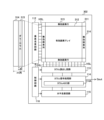
- FIG. 2 is a block diagram showing an example of the configuration of a solid-state imaging device according to the first embodiment.
- the solid-state imaging device 102 includes a pixel array section 111, a vertical scanning circuit 112, a column readout circuit 113, a column signal processing section 114, a horizontal scanning circuit 115, and a control circuit 116.
- the pixel array section 111 includes a dummy pixel DIX and a plurality of pixels PIX.
- the pixel array section 111 may be provided with a dummy column DCA in which the dummy pixels DIX are arranged in a column direction.
- the pixels PIX are arranged in a matrix along the row direction (also called the horizontal direction) and the column direction (also called the vertical direction).
- Each dummy pixel DIX and each pixel PIX may include an effective pixel capable of receiving incident light and a light-shielded OPB pixel.
- Each dummy pixel DIX and each pixel PIX may be sensitive to visible light, may be sensitive to near infrared light (NIR: Near InfraRed), may be sensitive to shortwave infrared light (SWIR: Short Wavelength InfraRed), may be sensitive to ultraviolet light, X-rays, or the like.
- NIR Near InfraRed
- SWIR Short Wavelength InfraRed
- each pixel PIX may be arranged in a Bayer array or a quad Bayer array.
- each dummy pixel DIX and each pixel PIX is sensitive to infrared light, in order to improve conversion efficiency, each dummy pixel DIX and each pixel PIX may be configured with a Hall sensor. In a Hall sensor, holes can be generated more efficiently than electrons during photoelectric conversion.
- Each dummy pixel DIX and each pixel PIX can form a source follower with the column readout circuit 113 when reading out a signal.
- the dummy pixel DIX and each pixel PIX are connected to a horizontal drive line HSL for each row.
- the dummy pixel DIX is connected to a dummy signal line DSL for each column, and the pixel PIX is connected to a vertical signal line VSL for each column.
- the horizontal drive line HSL drives each dummy pixel DIX and each pixel PIX for each row when reading out a signal from each dummy pixel DIX and each pixel PIX.
- the vertical signal line VSL transmits the signal read out from the pixel PIX to the column signal processing unit 114 for each column.
- the dummy signal line DSL connects each dummy pixel DIX to a current source.
- the vertical scanning circuit 112 scans the pixels PIX to be read in the column direction.
- the vertical scanning circuit 112 may be configured to include a vertical register.
- the vertical scanning circuit 112 can drive each pixel PIX row by row via the horizontal drive line HSL.
- the column readout circuit 113 can form a source follower with each pixel PIX when reading out a signal from the pixel PIX. At this time, the column readout circuit 113 can change the potential of the vertical signal line VSL based on the charge held in the pixel PIX.
- the column readout circuit 113 can connect the vertical signal lines VSL of each column to each other during the non-readout period. Then, the column readout circuit 113 can control the potential of the vertical signal line VSL of each column based on the potential of the dummy signal line DSL. At this time, the column readout circuit 113 can control the dummy signal line DSL and the vertical signal line VSL of each column to have the same potential. This control may be performed during the vertical blanking period or the horizontal blanking period.
- the column signal processing unit 114 processes signals transmitted in the column direction from each pixel PIX.
- the column signal processing unit 114 can perform correlated double sampling (CDS) processing based on the signals transmitted in the column direction from each pixel PIX.
- CDS correlated double sampling
- the column signal processing unit 114 can also perform AD (Analog to Digital) conversion processing based on the signals transmitted in the column direction from each pixel PIX, and output the image signal Gout.
- AD Analog to Digital
- the column signal processing unit 114 includes a column ADC unit 114A.
- the column ADC unit 114A can perform AD conversion processing in parallel for each column. At this time, the column ADC unit 114A can perform AD conversion for each column based on the result of comparing the pixel signal read out from the pixel PIX with a reference signal.
- the column readout circuit 113 and the column signal processing unit 114 may be located on both sides of the pixel array unit 111 in the column direction.
- the horizontal scanning circuit 115 scans the pixels PIX to be read in the row direction.
- the horizontal scanning circuit 115 may be configured to include a horizontal register.
- the control circuit 116 controls the vertical scanning circuit 112, the column readout circuit 113, the column signal processing unit 114, and the horizontal scanning circuit 115.
- the control circuit 116 can control the scanning timing in the column direction, the scanning timing in the row direction, the operation timing of the column readout circuit 113, and the processing timing of the column signal processing unit 114.
- the control circuit 116 can also set the timing at which the potential of the vertical signal line VSL of each column is controlled based on the potential of the dummy signal line DSL.
- the control circuit 116 can set this timing to the vertical blanking period or the horizontal blanking period.
- the control circuit 116 includes a mode setting unit 116A.
- the mode setting unit 116A can set a mode that controls the potential of the vertical signal line VSL of each column based on the potential of the dummy signal line DSL. This mode can switch the current consumption during the readout period. At this time, the mode setting unit 116A can set a normal mode, a low power consumption mode, and a standby mode.
- the control circuit 116 is an example of a control unit described in the claims.
- FIG. 3 is a block diagram showing an example of the circuit configuration of a pixel provided in a solid-state imaging device according to the first embodiment.
- pixel PIX includes a photodiode 121, a transfer transistor 122, a reset transistor 123, an amplification transistor 124, a selection transistor 125, and a floating diffusion FD.
- MOS Metal Oxide Semiconductor
- the amplification transistor 124 and the selection transistor 125 are connected in series.
- the cathode of the photodiode 121 is connected to the floating diffusion FD via the transfer transistor 122.
- the floating diffusion FD is connected to the power supply VDD via the reset transistor 123.
- the power supply VDD is connected to the vertical signal line VSL via the series circuit of the amplification transistor 124 and the selection transistor 125.
- the gate of the amplification transistor 124 is connected to the floating diffusion FD.
- a transfer signal TGL is applied to the gate of the transfer transistor 122.
- a reset signal RST is applied to the gate of the reset transistor 123.
- a selection signal SEL is applied to the gate of the selection transistor 125.
- the transfer signal TGL, reset signal RST, and selection signal SEL can be transmitted to each pixel PIX via the horizontal drive line HSL in FIG. 2.
- the transfer transistor 122 When the transfer transistor 122 is turned on, the charge accumulated in the photodiode 121 is transferred to the floating diffusion FD. Then, when the selection transistor 125 is turned on, the source potential of the amplification transistor 124 changes according to the potential of the floating diffusion FD. Then, the source potential of the amplification transistor 124 is applied to the vertical signal line VSL via the selection transistor 125, and transmitted via the vertical signal line VSL. Also, when the reset transistor 123 is turned on, the charge accumulated in the floating diffusion FD is discharged.
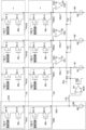
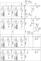
- FIG. 4 is a diagram showing an example of the configuration of a column readout circuit provided in a solid-state imaging device according to the first embodiment.
- the pixel array section 111 is provided with an effective pixel region 131 and an OPB pixel region 231.
- a dummy effective pixel DVX and effective pixels PVX1 to PVX3, etc. are arranged in the effective pixel region 131.
- a dummy OPB pixel DBX and OPB pixels PBX1 to PBX3, etc. are arranged in the OPB pixel region 231.
- the dummy effective pixel DVX and the dummy OPB pixel DBX are arranged in a dummy column DCA.
- Dummy effective pixel DVX includes pixel circuit 132-0, amplifier transistor 124-0, and selection transistor 125-0.
- Dummy OPB pixel DBX includes pixel circuit 232-0, amplifier transistor 224-0, and selection transistor 225-0.
- Each effective pixel PVX1 to PVX3 includes pixel circuits 132-1 to 132-3, amplifier transistors 124-1 to 124-3, and selection transistors 125-1 to 125-3.
- Each OPB pixel PBX1 to PBX3 includes pixel circuits 232-1 to 232-3, amplifier transistors 224-1 to 224-3, and selection transistors 225-1 to 225-3.
- Each pixel circuit 132-0 to 132-3, 232-0 to 232-3 can include a photodiode 121, a transfer transistor 122, a reset transistor 123, and a floating diffusion FD.
- the dummy effective pixel DVX and the dummy OPB pixel DBX are connected to a dummy signal line DSL.
- Each of the effective pixels PVX1 to PVX3... and each of the OPB pixels PBX1 to PBX3... are connected to vertical signal lines VSL1 to VSL3..., respectively.
- the selection transistor 225-0 of the dummy OPB pixel DBX can be turned on/off independently of the selection transistor 125-0 of the dummy effective pixel DVX, the selection transistors 125-1 to 125-3... of each of the effective pixels PVX1 to PVX3..., and the selection transistors 225-1 to 225-3... of each of the OPB pixels PBX1 to PBX3....
- the dummy signal line DSL is connected to the current source 160 via the switch 180.
- the dummy signal line DSL is also connected to the inverting input terminal of the operational amplifier 191 via the switch 170.
- the vertical signal lines VSL1 to VSL3 are connected to the current sources 161 to 163 via the switches 181 to 183, respectively.
- the vertical signal lines VSL1 to VSL3 are connected to the horizontal connecting signal line HCL via the switches 171 to 173, respectively.
- the switches 170 to 173, 180 to 183 may be field effect transistors.
- the non-inverting input terminal of the operational amplifier 191 and the drain of the drive transistor 192 are connected to the horizontal connecting signal line HCL.
- the output of the operational amplifier 191 is connected to the gate of the drive transistor 192.
- the operational amplifier 191 can compare the potential of the dummy signal line DSL with the potential of the horizontal connecting signal line HCL, and drive the drive transistor 192 so that the dummy signal line DSL and the horizontal connecting signal line HCL are at the same potential.
- the drive transistor 192 may be a field effect transistor.
- Each of the comparators 151 to 153... is connected to the vertical signal lines VSL1 to VSL3. At this time, the potentials of the vertical signal lines VSL1 to VSL3... are applied to the inverting inputs of each of the comparators 151 to 153....
- a reference signal DAC is input to the non-inverting inputs of each of the comparators 151 to 153....
- the reference signal DAC is, for example, a ramp signal. Then, each of the comparators 151 to 153... can compare the potentials of the vertical signal lines VSL1 to VSL3 with the reference signal DAC, and output the comparison results VO1 to VO3.
- the control circuit 116 can turn off the switches 181 to 183... and turn on the switches 170 to 173... and 180.
- the vertical scanning circuit 112 also turns on the selection transistor 225-0 of the dummy OPB pixel DBX and turns off the selection transistor 125-0 of the dummy effective pixel DVX, the selection transistors 125-1 to 125-3... of each effective pixel PVX1 to PVX3..., and the selection transistors 225-1 to 225-3... of each OPB pixel PBX1 to PBX3.
- the column readout circuit 113 can control the dummy signal line DSL and the vertical signal line VSL of each column so that they are at the same potential.
- the control circuit 116 can turn on the switches 181 to 183... and turn off the switches 170 to 173... and 180.
- the vertical scanning circuit 112 turns off the selection transistor 225-0 of the dummy OPB pixel DBX and the selection transistor 125-0 of the dummy effective pixel DVX, and turns on the selection transistors 125-1 to 125-3... of each effective pixel PVX1 to PVX3... and the selection transistors 225-1 to 225-3... of each OPB pixel PBX1 to PBX3.
- the column ADC unit 114A can AD convert the pixel signals read out from each pixel PVX1 to PVX3 based on the comparison results VO1 to VO3 output from each comparator 151 to 153....
- control circuit 116 can independently control the on/off state of the switch 180 and the on/off state of the switches 181 to 183.... For example, when the switches 181 to 183... are on, the control circuit 116 may turn on the switch 180 or may turn off the switch 180. Here, by turning off the switch 180 when the switches 181 to 183... are on, the current flowing through the dummy signal line DSL during the read period can be cut off, thereby achieving low power consumption.
- the control circuit 116 also inputs a mode setting signal MOD to the operational amplifier 191.
- the mode setting signal MOD can set the normal mode, the low power consumption mode, and the standby mode.
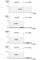
- FIG. 5 is a timing chart showing an example of a readout period and a non-readout period of the solid-state imaging device according to the first embodiment.
- a vertical period H6 for one frame is set in accordance with the vertical synchronization signal XVS.
- a waiting period H1 may be provided before the vertical period H6.
- a vertical readout period H2 and a vertical blanking period H3 are set in each vertical period H6.
- a non-exposure period H4 and an exposure period H5 are also set in each vertical period H6.
- the switches 181 to 183 are off, the switches 170 to 173, 180 are turned on.
- the vertical signal lines VSL1 to VSL3 are connected to the horizontal connecting signal line HCL via the switches 171 to 173.
- the dummy signal line DSL is connected to the current source 160.
- the operational amplifier 191 drives the drive transistor 192 so that the dummy signal line DSL and the horizontal connecting signal line HCL are at the same potential. This suppresses the rise in the potential VL2 of the vertical signal lines VSL1 to VSL3 during the vertical blanking period H3, and suppresses the occurrence of horizontal stripes caused by the coupling CUP between the vertical signal lines VSL1 to VSL3 and the pixels.
- FIG. 6 is a timing chart showing an example of waveforms of vertical signal lines during a horizontal blanking period and an AD conversion period of a solid-state imaging device according to the first embodiment. Note that in the figure, the potentials VL1 and VL2 of the vertical signal lines are shown with inverted polarity.
- a horizontal blanking period H11 and a horizontal readout period H12 are set based on a horizontal enable signal H11.
- Each horizontal readout period H12 is provided with a P-phase AD conversion period PAD and a D-phase AD conversion period DAD.
- the switches 181 to 183... are turned off, and the vertical signal lines VSL1 to VSL3... are respectively disconnected from the current sources 161 to 163.
- the potential VL1 of the vertical signal lines VSL1 to VSL3... rises based on the off-leakage from the selection transistor 125.
- the switches 181 to 183 are off, the switches 170 to 173, 180 are turned on.
- the vertical signal lines VSL1 to VSL3 are connected to the horizontal connecting signal line HCL via the switches 171 to 173.
- the dummy signal line DSL is connected to the current source 160.
- the operational amplifier 191 drives the drive transistor 192 so that the dummy signal line DSL and the horizontal connecting signal line HCL are at the same potential. This prevents the rise in the potential VL2 of the vertical signal lines VSL1 to VSL3 during the horizontal blanking period H11.
- the potential VL2 of the vertical signal lines VSL1 to VSL3 can be set to any level, and the settling time can be shortened. This makes it possible to increase the proportion (duty ratio) of the horizontal blanking period H11 in one horizontal period, thereby reducing power consumption during the horizontal blanking period H11.
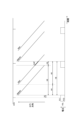
- FIG. 7 is a diagram showing the relationship between the load current and the control current in each mode of the solid-state imaging device according to the first embodiment.
- a in the figure shows the current flowing through the vertical signal lines VSL1 to VSL3... in the constant current mode (when the switches 181 to 183... are turned on during the vertical blanking period).
- b in the figure shows the current flowing through the vertical signal lines VSL1 to VSL3... in the normal mode when the switches 181 to 183... are turned off during the vertical blanking period.
- c in the figure shows the current flowing through the vertical signal lines VSL1 to VSL3... in the standby mode when the switches 181 to 183... are turned off during the vertical blanking period.
- d in the figure shows the current flowing through the vertical signal lines VSL1 to VSL3... in the low power consumption mode when the switches 181 to 183... are turned off during the vertical blanking period.
- the current consumption during the readout period and vertical blanking period is IPAmA.
- the current consumption during the readout period is IPBmA
- the current consumption during the vertical blanking period is IPCmA.
- IPB IPA + IPC.
- the current consumption during the readout period increases compared to the constant current mode, but the current consumption during the vertical blanking period decreases.
- the number of vertical signal lines VSL is greater than the number of dummy signal lines DSL. Therefore, the increase in current consumption during the readout period is small, but the decrease in current consumption during the vertical blanking period is large. Therefore, in this normal mode, power consumption can be reduced compared to the constant current mode.
- the current consumption during the readout period is IPAmA
- the current consumption during the vertical blanking period is IPCmA.
- the current consumption during the readout period is equal to the current consumption in the constant current mode, but the current consumption during the vertical blanking period is reduced compared to the constant current mode. Therefore, in this standby mode, power consumption can be reduced compared to normal mode.
- the current consumption during the readout period is IPAmA+ ⁇
- the current consumption during the vertical blanking period is IPCmA.
- the current consumption is slightly higher than in the constant current mode, and the current consumption during the vertical blanking period is lower than in the constant current mode. Therefore, in this low power consumption mode, power consumption can be reduced compared to the constant current mode.
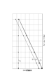
- FIG. 8 is a diagram showing the relationship between the frame rate and current consumption in each mode of the solid-state imaging device according to the first embodiment. Note that L1 indicates the constant current mode, L2 indicates the normal mode, L3 indicates the low power consumption mode, and L4 indicates the standby mode.
- normal mode L2, low power consumption mode L3, and standby mode L4 are more effective at reducing power consumption at low frame rates such as long exposure times than constant current mode L1.
- normal mode L2 may result in increased power consumption at high frame rates compared to constant current mode L1. For this reason, at high frame rates where the frame rate is fixed, operation may be performed in constant current mode L1. Alternatively, operation may be performed in low power consumption mode L3 or standby mode L4 during the readout period.
- the potential of the horizontal connecting signal line HCL connecting the vertical signal lines VSL1 to VSL3... is controlled based on the potential of the dummy signal line DSL connected to the dummy pixels provided in the dummy column DCA.
- the potential of the horizontal connection signal line HCL is controlled based on the potential of the dummy signal line DSL connected to the dummy pixel provided in the dummy column DCA.
- a plurality of dummy columns are provided in which dummy pixels connected to the dummy signal lines are arranged in the column direction.
- FIG. 9 shows an example of the configuration of a light detection device according to the second embodiment.
- the imaging device has dummy columns DCA1 and DCA2 instead of the dummy column DCA of the first embodiment described above.
- the rest of the configuration of the imaging device of the second embodiment is the same as the configuration of the imaging device of the first embodiment described above.
- Each of the dummy columns DCA1 and DCA2 can be configured in the same way as the dummy column DCA.
- the dummy effective pixel DVX1 and the dummy OPB pixel DBX1 are arranged in the dummy column DCA1.
- the dummy effective pixel DVX2 and the dummy OPB pixel DBX2 are arranged in the dummy column DCA2.
- the dummy effective pixel DVX1 includes a pixel circuit 132-01, an amplifier transistor 124-01, and a selection transistor 125-01.
- the dummy OPB pixel DBX1 includes a pixel circuit 232-01, an amplifier transistor 224-01, and a selection transistor 225-01.
- the dummy effective pixel DVX1 and the dummy OPB pixel DBX1 are connected to a dummy signal line DSL1.
- the dummy signal line DSL1 is connected to a current source 160-1 via a switch 180-1.
- the dummy signal line DSL1 is also connected to the inverting input terminal of an operational amplifier 191 via a switch 170.
- the dummy effective pixel DVX2 includes a pixel circuit 132-02, an amplifier transistor 124-02, and a selection transistor 125-02.
- the dummy OPB pixel DBX2 includes a pixel circuit 232-02, an amplifier transistor 224-02, and a selection transistor 225-02.
- the dummy effective pixel DVX2 and the dummy OPB pixel DBX2 are connected to a dummy signal line DSL2.
- the dummy signal line DSL2 is connected to a current source 160-2 via a switch 180-2.
- the dummy signal line DSL2 is also connected to the inverting input terminal of an operational amplifier 191 via a switch 170.
- Each pixel circuit 132-01, 132-02, 232-01, 232-02 can include a photodiode 121, a transfer transistor 122, a reset transistor 123, and a floating diffusion FD.
- the potentials of the multiple dummy signal lines DSL1, DSL2 are averaged and input to the non-inverting input of the operational amplifier 191.
- the operational amplifier 191 compares the average value of the potentials of the dummy signal lines DSL1, DSL2 with the potential of the horizontal connecting signal line HCL. Then, the operational amplifier 191 can drive the drive transistor 192 so that the average value of the potentials of the dummy signal lines DSL1, DSL2 and the horizontal connecting signal line HCL are at the same potential.
- multiple dummy columns DCA1, DCA2 are provided in which dummy pixels connected to each dummy signal line DSL1, DSL2 are arranged in the column direction.
- the potential of the horizontal connection signal line HCL is controlled based on the potential of the dummy signal line DSL connected to the dummy pixel provided in the dummy column DCA.
- n columns of dummy columns are provided in part of m columns of ineffective pixels provided around the effective pixel array.
- FIG. 10 is a block diagram showing an example of the configuration of a solid-state imaging device according to the third embodiment.
- solid-state imaging device 302 has pixel array section 311 instead of pixel array section 111 of the first embodiment described above.
- the rest of the configuration of solid-state imaging device 302 of the third embodiment is similar to the configuration of solid-state imaging device 102 of the first embodiment described above.
- the pixel array section 311 includes an effective pixel array 312, an ineffective pixel row 313, and an ineffective pixel column 314.
- the ineffective pixel row 313 may be arranged on both sides of the effective pixel array 312 in the column direction.
- the ineffective pixel column 314 may be arranged on both sides of the effective pixel array 312 in the row direction.
- valid pixels are arranged in a matrix along the row and column directions.
- invalid pixels are arranged along the row direction.
- invalid pixels are arranged along the column direction. Only m invalid pixel columns 314 can be provided. In this case, n dummy columns 315 can be provided in the invalid pixel column 314.
- dummy pixels are arranged in the column direction. The dummy pixels can be provided with dummy valid pixels and dummy OPB pixels.
- the dummy column 315 is connected to a dummy signal line DSL.
- the configuration of one column of the dummy column 315 can be configured in the same way as the dummy column DCA of the first embodiment described above.
- dummy columns 315 are provided in some of the invalid pixel rows 314 provided around the valid pixel array 312. This makes it possible to arrange n rows of dummy pixels around the valid pixel array 312.
- a pixel in which electrons are accumulated based on photoelectric conversion is applied to a solid-state imaging device.
- a pixel in which holes are accumulated based on photoelectric conversion is applied to a solid-state imaging device.
- FIG. 11 is a diagram showing an example of the circuit configuration of a pixel provided in a solid-state imaging device according to the fourth embodiment.
- pixel PHX has a photodiode 410, a transfer transistor 412, and a reset transistor 413 instead of the photodiode 121, transfer transistor 122, and reset transistor 123 of pixel PIX of the first embodiment described above. Furthermore, pixel PHX has capacitors SN1, SN2, and a discharge transistor 414 added to pixel PIX of the first embodiment described above.
- the amplification transistor 124 and selection transistor 125 may be N-channel field effect transistors.
- the transfer transistor 412, reset transistor 413, and discharge transistor 414 may be P-channel field effect transistors.
- Capacitors SN1 and SN2 may be MIM (Metal Insulation Metal) capacitances or junction capacitances formed on a semiconductor substrate.
- the photodiode 410 generates holes based on photoelectric conversion.
- the material of the photodiode 410 can be, for example, InGaP, InAlP, InGaAs, InAlAs, or a compound semiconductor with a chalcopyrite structure.
- the photodiode 410 can be made sensitive to infrared light (for example, a wavelength band of 900 nm to 1700 nm).
- a power supply voltage Vtop is applied to the anode of the photodiode 410.
- the power supply voltage Vtop is variable depending on a reset voltage for initializing the charge of the photodiode 410.
- the transfer transistor 412 transfers the charge stored in the photodiode 410 to the floating diffusion FD.
- the reset transistor 413 resets the charge stored in the floating diffusion FD.
- the discharge transistor 414 discharges the charge stored in the capacitor SN1.
- the amplification transistor 124 and the selection transistor 125 are connected in series.
- the series circuit of the amplification transistor 124 and the selection transistor 125 is connected between the power supply voltage VDD3 and the vertical signal line VSL.
- the cathode of the photodiode 410 is connected to the floating diffusion FD via the transfer transistor 412.
- the floating diffusion FD is also connected to the power supply voltage VDD1 via the reset transistor 123.
- the voltage VDD1 is lower than the power supply voltage Vtop.
- Capacitor SN1 is connected to the anode of the photodiode 410.
- the transfer transistor 412 and the discharge transistor 414 are connected in series.
- the series circuit of the transfer transistor 412 and the discharge transistor 414 is connected between the power supply voltage VDD1 and the floating diffusion FD.
- Capacitor SN2 is connected to the floating diffusion FD.
- a transfer signal TGL is applied to the gate of the transfer transistor 412.
- a reset signal PST is applied to the gate of the reset transistor 413.
- a discharge signal OFG is applied to the gate of the discharge transistor 414.
- the pixel PHX in which holes are accumulated based on photoelectric conversion is applied to a solid-state imaging device. This makes it possible to reduce power consumption while suppressing the occurrence of horizontal stripes caused by coupling between the vertical signal line VSL and the pixel PHX, and also improve sensitivity in the infrared region.
- the potential of the horizontal connecting signal line HCL connecting the vertical signal lines VSL1 to VSL3, etc. is controlled based on the potential of the dummy signal line DSL connected to the dummy pixel provided in the dummy column DCA.
- semiconductor chips on which a solid-state imaging device is formed, the solid-state imaging device having a pixel array portion in which pixels are arranged in a matrix, are stacked.
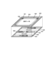
- FIG. 12 is a perspective view showing an example of a stack of a solid-state imaging device according to the fifth embodiment.
- the solid-state imaging device includes semiconductor chips 921 and 922.
- Semiconductor chip 922 is stacked on semiconductor chip 921.
- a pixel array section 923 is formed in the semiconductor chip 922.
- pixels 931 are arranged in a matrix in the row and column directions.
- the pixels 931 may be pixels PIX in FIG. 3 or pixels PHX in FIG. 11.
- a pad electrode 932 and a via electrode 933 are formed around the pixel array section 923.
- the via electrode 933 passes through the semiconductor chip 922 and can electrically connect the semiconductor chips 921 and 922 to each other.
- a peripheral circuit 924 is formed on the semiconductor chip 921.
- a column readout circuit 925, a column ADC 926, a communication interface 927, and an oscillator circuit 928 are formed on the peripheral circuit 924.
- the column readout circuit 925 and the column ADC 926 may be formed to correspond to positions on both sides of the pixel array section 923 in the column direction.
- the semiconductor chips 921 and 922 may be directly bonded. Hybrid bonding may be used for directly bonding the semiconductor chips 921 and 922. In this case, the semiconductor chips 921 and 922 may be electrically connected based on a Cu-Cu connection.
- the material of the semiconductor substrate used for the semiconductor chips 921 and 922 may be Si, InGaAs, or InP.
- the semiconductor chip 922 in which the pixel array section 923 is formed is stacked on the semiconductor chip 921 in which the peripheral circuit 924 is formed. This makes it possible to increase the sensitivity of the solid-state imaging device while suppressing an increase in the mounting area of the semiconductor chip in which the solid-state imaging device is formed.
- the above-described embodiment shows an example for realizing the present technology, and there is a corresponding relationship between the matters in the embodiment and the matters specifying the invention in the claims. Similarly, there is a corresponding relationship between the matters specifying the invention in the claims and the matters in the embodiment of the present technology that have the same name.
- the present technology is not limited to the embodiment, and can be realized by making various modifications to the embodiment without departing from the gist of the technology.
- the effects described in this specification are merely examples and are not limiting, and other effects may also be present.
- the present technology can also be configured as follows. (1) a first signal line connected to a first effective pixel; a first current source connected to the first signal line; a first switch provided between the first effective pixel and the first current source; a second signal line connected to the second effective pixel; a second current source connected to the second signal line; a second switch provided between the second effective pixel and the second current source; a horizontal connecting signal line connecting the first signal line and the second signal line; A dummy signal line connected to the dummy pixel; a third current source connected to the dummy signal line; a control unit that controls a potential of the horizontal-connection signal line based on a potential of the dummy signal line.
- the control unit includes an operational amplifier having a first input connected to the dummy signal line and a second input connected to the horizontal connecting signal line.
- the control unit includes a transistor that drives the horizontal connection signal line based on an output of the operational amplifier.
- the control unit includes a mode setting unit that sets a current flowing through the transistor during a readout period.
- the photodetection device according to any one of (1) to (5), wherein the dummy pixels include OPB (Opitical Black) pixels.
- a third switch provided between the first signal line and the horizontal connecting signal line;
- the first switch and the second switch are turned off during a vertical blanking period;
- the first switch and the second switch are turned off during a horizontal blanking period;
- the first column includes the first effective pixel and a first OPB pixel; the second column includes the second effective pixel and a second OPB pixel;
- the photodetection device according to (13), wherein the dummy column includes a dummy effective pixel and a dummy OPB pixel.
- Imaging device 101 Optical system 102 Solid-state imaging device 103 Imaging control unit 104 Image processing unit 105 Memory unit 106 Display unit 107 Operation unit 108 Bus 111 Pixel array unit 112 Vertical scanning circuit 113 Column readout circuit 114 Column signal processing unit 115 Horizontal scanning circuit 116 Control circuit 121 Photodiode 122 Transfer transistor 123 Reset transistor 124 Amplification transistor 125 Selection transistor PIX Pixel DIX Dummy pixel HSL Horizontal drive line VSL Vertical signal line HCL Horizontal connection signal line DSL Dummy signal line DCA Dummy column 132-0 to 132-3, 232-0 to 232-3 Pixel circuit 151 to 153 Comparator 161 to 163 Current source 170 to 173, 180 to 183 Switch 191 Operational amplifier 192 Drive transistor 131 Effective pixel area 231 OPB pixel area DVX Dummy effective pixel DBX Dummy OPB pixel PVX Effective pixel PBX OPB pixel
Landscapes
- Engineering & Computer Science (AREA)
- Multimedia (AREA)
- Signal Processing (AREA)
- Transforming Light Signals Into Electric Signals (AREA)
Abstract
画質の低下を抑制しつつ、非読出し期間の負荷トランジスタの電流を低減する。 光検出装置は、第1の有効画素に接続される第1の信号線と、第1の信号線に接続される第1の電流源と、第1の有効画素と第1の電流源との間に設けられる第1のスイッチと、第2の有効画素に接続される第2の信号線と、第2の信号線に接続される第2の電流源と、第2の有効画素と第2の電流源との間に設けられる第2のスイッチと、第1の信号線と第2の信号線とを接続する横つなぎ信号線と、ダミー画素に接続されるダミー信号線と、ダミー信号線に接続される第3の電流源と、ダミー信号線の電位に基づいて、横つなぎ信号線の電位を制御する制御部とを備える。
Description
本技術は、光検出装置に関する。詳しくは、垂直信号線を介して画素と負荷トランジスタとの間でソースフロアを構成可能な光検出装置に関する。
撮像装置の低消費電力化を図るため、非読出し期間に垂直信号線と負荷トランジスタとを切り離す方法がある。例えば、A/D変換部のコンパレータが反転した後は、負荷MOS回路では電流の供給を停止させ、消費電力の低減を図るようにした固体撮像装置が提案されている(例えば、特許文献1参照)。
しかしながら、非読出し期間に負荷トランジスタの電流を停止させると、非読出し期間の垂直信号線の電位が読出し期間の垂直信号線の電位と乖離し、容量カップリングにより、画質の低下を招くおそれがあった。
本技術はこのような状況に鑑みて生み出されたものであり、画質の低下を抑制しつつ、非読出し期間の負荷トランジスタの電流を低減することを目的とする。
本技術は、上述の問題点を解消するためになされたものであり、その第1の側面は、第1の有効画素に接続される第1の信号線と、前記第1の信号線に接続される第1の電流源と、前記第1の有効画素と前記第1の電流源との間に設けられる第1のスイッチと、第2の有効画素に接続される第2の信号線と、前記第2の信号線に接続される第2の電流源と、前記第2の有効画素と前記第2の電流源との間に設けられる第2のスイッチと、前記第1の信号線と前記第2の信号線とを接続する横つなぎ信号線と、ダミー画素に接続されるダミー信号線と、前記ダミー信号線に接続される第3の電流源と、前記ダミー信号線の電位に基づいて、前記横つなぎ信号線の電位を制御する制御部とを備える光検出装置である。これにより、非読出し期間に負荷トランジスタの電流を停止させつつ、非読出し期間の垂直信号線の電位と読出し期間の垂直信号線の電位との乖離が抑制されるという作用をもたらす。
また、第1の側面において、前記制御部は、前記ダミー信号線と前記横つなぎ信号線とが同電位となるように制御してもよい。これにより、非読出し期間に負荷トランジスタの電流を停止させつつ、非読出し期間の垂直信号線の電位が読出し期間の垂直信号線の電位と一致されるという作用をもたらす。
また、第1の側面において、前記制御部は、第1入力が前記ダミー信号線に接続され、第2入力が前記横つなぎ信号線に接続されるオペアンプを備えてもよい。これにより、ダミー信号線の電位と横つなぎ信号線の電位とが比較されるという作用をもたらす。
また、第1の側面において、前記制御部は、前記オペアンプの出力に基づいて、前記横つなぎ信号線を駆動するトランジスタを備えてもよい。これにより、ダミー信号線の電位と横つなぎ信号線の電位との比較結果に基づいて、横つなぎ信号線の電位が制御されるという作用をもたらす。
また、第1の側面において、前記制御部は、読出し期間に前記トランジスタに流れる電流を設定するモード設定部を備えてもよい。これにより、読出し期間にトランジスタに流れる電流が制御されるという作用をもたらす。
また、第1の側面において、前記ダミー画素は、OPB(Opitical Black)画素を含んでもよい。これにより、光検出装置の特性の製造バラツキに対応しつつ、非読出し期間の垂直信号線の電位が読出し期間の垂直信号線の電位と一致されるという作用をもたらす。
また、第1の側面において、前記第1の信号線と前記横つなぎ信号線との間に設けられる第3のスイッチと、前記第2の信号線と前記横つなぎ信号線との間に設けられる第4のスイッチとをさらに備えてもよい。これにより、読出し期間に第1および第2の信号線と横つなぎ信号線との切り離しが可能となるという作用をもたらす。
また、第1の側面において、前記第1のスイッチおよび前記第2のスイッチは垂直ブランキング期間にオフされ、前記第3のスイッチおよび前記第4のスイッチは前記垂直ブランキング期間にオンされてもよい。これにより、垂直ブランキング期間に負荷トランジスタの電流を停止させつつ、垂直ブランキング期間の垂直信号線の電位が読出し期間の垂直信号線の電位と一致されるという作用をもたらす。
また、第1の側面において、前記第1のスイッチおよび前記第2のスイッチは水平ブランキング期間にオフされ、前記第3のスイッチおよび前記第4のスイッチは前記水平ブランキング期間にオンされてもよい。これにより、水平ブランキング期間に負荷トランジスタの電流を停止させつつ、水平ブランキング期間の垂直信号線の電位が読出し期間の垂直信号線の電位と一致されるという作用をもたらす。
また、第1の側面において、前記ダミー画素と前記第3の電流源との間に設けられる第5のスイッチをさらに備えてもよい。これにより、読出し期間にダミー画素と第3の電流源とが切り離されるという作用をもたらす。
また、第1の側面において、前記第5のスイッチは、垂直ブランキング期間にオンされ、読出し期間にオフされてもよい。これにより、垂直ブランキング期間にダミー信号線に電流が流され、読出し期間にダミー信号線に流れる電流が停止されるという作用をもたらす。
また、第1の側面において、前記第5のスイッチは、水平ブランキング期間にオンされ、読出し期間にオフされてもよい。これにより、水平ブランキング期間にダミー信号線に電流が流され、読出し期間にダミー信号線に流れる電流が停止されるという作用をもたらす。
また、第1の側面において、前記第1の有効画素がカラム方向に配列された第1のカラムと、前記第2の有効画素が前記カラム方向に配列された第2のカラムと、前記ダミー画素が前記カラム方向に配列されたダミーカラムとを備えてもよい。これにより、有効画素がロウ方向およびカラム方向にマトリックス状に配置された画素アレイ部において、非読出し期間に負荷トランジスタの電流を停止させつつ、非読出し期間の垂直信号線の電位と読出し期間の垂直信号線の電位との乖離が抑制されるという作用をもたらす。
また、第1の側面において、前記第1のカラムは、前記第1の有効画素および第1のOPB画素を含み、前記第2のカラムは、前記第2の有効画素および第2のOPB画素を含み、前記ダミーカラムは、ダミー有効画素およびダミーOPB画素を含んでもよい。これにより、有効画素がロウ方向およびカラム方向にマトリックス状に配置された画素アレイ部において、光検出装置の特性の製造バラツキに対応しつつ、非読出し期間の垂直信号線の電位が読出し期間の垂直信号線の電位と一致されるという作用をもたらす。
また、第1の側面において、前記ダミーカラムは複数設けられてもよい。これにより、ダミーカラムの出力精度が向上されるという作用をもたらす。
以下、本技術を実施するための形態(以下、実施の形態と称する)について説明する。説明は以下の順序により行う。
1.第1の実施の形態(ダミーカラムに設けられたダミー画素に接続されるダミー信号線の電位に基づいて、有効画素が接続される垂直信号線を接続する横つなぎ信号線の電位を制御する例)
2.第2の実施の形態(ダミー信号線に接続されるダミー画素がカラム方向に配列されたダミーカラムを複数設けた例)
3.第3の実施の形態(有効画素アレイの周囲に設けられたm(mは正の整数)列分の無効画素列の一部にn(nは、mより小さな正の整数)列分のダミーカラムを設けた例)
4.第4の実施の形態(画素にホールセンサを用いた例)
5.第5の実施の形態(固体撮像装置が形成される半導体チップを積層化した例)
1.第1の実施の形態(ダミーカラムに設けられたダミー画素に接続されるダミー信号線の電位に基づいて、有効画素が接続される垂直信号線を接続する横つなぎ信号線の電位を制御する例)
2.第2の実施の形態(ダミー信号線に接続されるダミー画素がカラム方向に配列されたダミーカラムを複数設けた例)
3.第3の実施の形態(有効画素アレイの周囲に設けられたm(mは正の整数)列分の無効画素列の一部にn(nは、mより小さな正の整数)列分のダミーカラムを設けた例)
4.第4の実施の形態(画素にホールセンサを用いた例)
5.第5の実施の形態(固体撮像装置が形成される半導体チップを積層化した例)
<1.第1の実施の形態>
図1は、第1の実施の形態に係る光検出装置を含む撮像装置の構成例を示す図である。なお、以下の説明では、光検出装置として固体撮像装置を例にとる。
図1は、第1の実施の形態に係る光検出装置を含む撮像装置の構成例を示す図である。なお、以下の説明では、光検出装置として固体撮像装置を例にとる。
同図において、撮像装置100は、光学系101、固体撮像装置102、撮像制御部103、画像処理部104、記憶部105、表示部106および操作部107を備える。撮像制御部103、画像処理部104、記憶部105、表示部106および操作部107は、バス108を介して互いに接続されている。なお、撮像装置100は、単体としても用いられてもよいし、スマートフォンなどの携帯端末に組み込まれてもよいし、認証装置や監視装置に組み込まれてもよいし、車両やドローンに組み込まれてもよい。
光学系101は、被写体からの光を固体撮像装置102に入射させ、光学像を固体撮像装置102の受光面に結像させる。光学系101は、例えば、フォーカスレンズ、ズームレンズおよび絞りなどを備えることができる。光学系101は、広角レンズ、標準レンズおよび望遠レンズなどの複数のレンズを備えてもよい。
固体撮像装置102は、受光面に結像された光学像を画素ごとに電気信号に変換し、その電気信号をデジタル化して出力する。固体撮像装置102は、例えば、CMOS(Complementary Metal Oxide Semiconductor)イメージセンサである。CMOSイメージセンサは、裏面照射型イメージセンサでもよいし、表面照射型イメージセンサでもよい。なお、光検出装置は、固体撮像装置102に限定されず、ToF(Time of Flight)センサやイベントベースビジョンセンサなどに適用されてもよい。
撮像制御部103は、操作部107からの指令に基づいて固体撮像装置102による撮像を制御する。このとき、撮像制御部103は、固体撮像装置102の露光時間、露光量および撮像タイミングなどを制御することができる。
画像処理部104は、固体撮像装置102からの出力に基づいて画像処理を実施する。画像処理は、例えば、ガンマ補正、ホワイトバランス処理、シャープネス処理、階調変換処理である。画像処理部104は、ソフトウェアに基づいて処理を実行するプロセッサを備えてもよい。
記憶部105は、固体撮像装置102で撮像された撮像画像を記憶したり、固体撮像装置102の撮像パラメータなどを記憶したりする。また、記憶部105は、ソフトウェアに基づいて撮像装置100を動作させるプログラムを記憶することができる。記憶部105は、ROM(Read Only Memory)、RAM(Random Access Memory)およびメモリカードを含んでもよい。
表示部106は、撮像画像を表示したり、撮像操作をサポートする各種情報を表示したりする。表示部106は、液晶ディスプレイでもよいし、有機EL(Electro Luminescence)ディスプレイでもよい。
操作部107は、撮像装置100を操作するユーザインターフェースを提供する。操作部107は、例えば、撮像装置100に設けられたボタン、ダイヤルおよびスイッチを含んでもよい。操作部107は、表示部106とともにタッチパネルで構成してもよい。
なお、撮像装置100の形態によっては、上述の機能の一部がなくてよいし、逆に開示していない機能をさらに有してもよい。
図2は、第1の実施の形態に係る固体撮像装置の構成例を示すブロック図である。
同図において、固体撮像装置102は、画素アレイ部111、垂直走査回路112、カラム読出し回路113、カラム信号処理部114、水平走査回路115および制御回路116を備える。
画素アレイ部111は、ダミー画素DIXおよび複数の画素PIXを備える。このとき、画素アレイ部111には、ダミー画素DIXをカラム方向に配列するダミーカラムDCAを設けることができる。画素PIXは、ロウ方向(水平方向とも言う)およびカラム方向(垂直方向とも言う)に沿ってマトリックス状に配列される。各ダミー画素DIXおよび各画素PIXは、入射光を受光可能な有効画素および遮光されたOPB画素を備えることができる。各ダミー画素DIXおよび各画素PIXは、可視光に感度を持ってもよいし、近赤外光(NIR:Near InfraRed)に感度を持ってもよいし、短波赤外光(SWIR:Short Wavelength InfraRed)に感度を持ってもよいし、紫外光またはX線などに感度を持ってもよい。なお、各画素PIXが可視光に感度を持つ場合、各画素PIXは、ベイヤ配列を構成してもよいし、クワッドベイヤ配列を構成してもよい。各ダミー画素DIXおよび各画素PIXが赤外光に感度を持つ場合、変換効率を向上させるため、各ダミー画素DIXおよび各画素PIXは、ホールセンサで構成されてもよい。ホールセンサでは、光電変換時に電子よりもホールを効率的に生成することができる。
各ダミー画素DIXおよび各画素PIXは、信号の読出し時にカラム読出し回路113との間でソースフォロワを構成することができる。ダミー画素DIXおよび各画素PIXは、ロウごとに水平駆動線HSLに接続される。また、ダミー画素DIXはカラムごとにダミー信号線DSLに接続され、画素PIXはカラムごとに垂直信号線VSLに接続される。水平駆動線HSLは、各ダミー画素DIXおよび各画素PIXからの信号の読出し時に各ダミー画素DIXおよび各画素PIXをロウごとに駆動する。垂直信号線VSLは、画素PIXから読出された信号をカラムごとにカラム信号処理部114に伝送する。ダミー信号線DSLは、各ダミー画素DIXを電流源に接続する。
垂直走査回路112は、読出し対象となる画素PIXをカラム方向に走査する。垂直走査回路112は、垂直レジスタを含んで構成してもよい。ここで、垂直走査回路112は、各画素PIXからの信号の読出し時に、水平駆動線HSLを介して各画素PIXをロウごとに駆動することができる。
カラム読出し回路113は、各画素PIXからの信号の読出し時に、各画素PIXとの間でソースフォロワを構成することができる。このとき、カラム読出し回路113は、画素PIXに保持された電荷に基づいて垂直信号線VSLの電位を変化させることができる。
また、カラム読出し回路113は、非読出し期間において、各カラムの垂直信号線VSLを互いに接続することができる。そして、カラム読出し回路113は、ダミー信号線DSLの電位に基づいて、各カラムの垂直信号線VSLの電位を制御することができる。このとき、カラム読出し回路113は、ダミー信号線DSLと各カラムの垂直信号線VSLとが同電位となるように制御することができる。この制御は、垂直ブランキング期間に実施されてもよいし、水平ブランキング期間に実施されてもよい。
カラム信号処理部114は、各画素PIXからカラム方向に伝送された信号を処理する。例えば、カラム信号処理部114は、各画素PIXからカラム方向に伝送された信号に基づいて、相関二重サンプリング(CDS:Correlated Double Sampling)処理を実施することができる。また、カラム信号処理部114は、各画素PIXからカラム方向に伝送された信号に基づいて、AD(Analog to Digital)変換処理を実施し、撮像信号Goutを出力することができる。
カラム信号処理部114は、カラムADC部114Aを備える。カラムADC部114Aは、AD変換処理をカラムごとに並列に実施することができる。このとき、カラムADC部114Aは、画素PIXから読出された画素信号と参照信号との比較結果に基づいてカラムごとにAD変換することができる。なお、カラム読出し回路113およびカラム信号処理部114は、カラム方向において、画素アレイ部111の両側にあってもよい。
水平走査回路115は、読出し対象となる画素PIXをロウ方向に走査する。水平走査回路115は、水平レジスタを含んで構成してもよい。
制御回路116は、垂直走査回路112、カラム読出し回路113、カラム信号処理部114および水平走査回路115を制御する。例えば、制御回路116は、カラム方向の走査タイミング、ロウ方向の走査タイミング、カラム読出し回路113の動作タイミングおよびカラム信号処理部114の処理タイミングを制御することができる。
また、制御回路116は、ダミー信号線DSLの電位に基づいて各カラムの垂直信号線VSLの電位が制御されるタイミングを設定することができる。制御回路116は、このタイミングを垂直ブランキング期間に設定してもよいし、水平ブランキング期間に設定してもよい。
制御回路116は、モード設定部116Aを備える。モード設定部116Aは、ダミー信号線DSLの電位に基づいて各カラムの垂直信号線VSLの電位を制御するモードを設定することができる。このモードは、読出し期間の消費電流を切り替えることができる。このとき、モード設定部116Aは、通常モード、低消費電力モードおよびスタンバイモードを設定することができる。なお、制御回路116は、特許請求の範囲に記載の制御部の一例である。
図3は、第1の実施の形態に係る固体撮像装置に設けられた画素の回路構成例を示すブロック図である。
同図において、画素PIXは、フォトダイオード121、転送トランジスタ122、リセットトランジスタ123、増幅トランジスタ124、選択トランジスタ125およびフローティングディフュージョンFDを備える。転送トランジスタ122、リセットトランジスタ123、増幅トランジスタ124および選択トランジスタ125として、MOS(Metal Oxide Semiconductor)トランジスタを用いることができる。
増幅トランジスタ124と選択トランジスタ125は、直列に接続されている。フォトダイオード121のカソードは、転送トランジスタ122を介してフローティングディフュージョンFDに接続されている。また、フローティングディフュージョンFDは、リセットトランジスタ123を介して電源VDDに接続されている。また、電源VDDは、増幅トランジスタ124と選択トランジスタ125の直列回路を介して垂直信号線VSLに接続されている。増幅トランジスタ124のゲートはフローティングディフュージョンFDに接続されている。
転送トランジスタ122のゲートには、転送信号TGLが印加される。リセットトランジスタ123のゲートには、リセット信号RSTが印加される。選択トランジスタ125のゲートには、選択信号SELが印加される。転送信号TGL、リセット信号RSTおよび選択信号SELは、図2の水平駆動線HSLを介して各画素PIXに伝送することができる。
転送トランジスタ122がオンすると、フォトダイオード121に蓄積された電荷がフローティングディフュージョンFDに転送される。そして、選択トランジスタ125がオンすると、フローティングディフュージョンFDの電位に応じて増幅トランジスタ124のソース電位が変化する。そして、増幅トランジスタ124のソース電位は、選択トランジスタ125を介して垂直信号線VSLに印加され、垂直信号線VSLを介して伝送される。また、リセットトランジスタ123がオンすると、フローティングディフュージョンFDに蓄積された電荷が排出される。
図4は、第1の実施の形態に係る固体撮像装置に設けられたカラム読出し回路の構成例を示す図である。
同図において、画素アレイ部111には、有効画素領域131およびOPB画素領域231が設けられる。有効画素領域131には、ダミー有効画素DVXおよび有効画素PVX1からPVX3・・が配置される。OPB画素領域231には、ダミーOPB画素DBXおよびOPB画素PBX1からPBX3・・が配置される。ダミー有効画素DVXおよびダミーOPB画素DBXは、ダミーカラムDCAに配置される。
ダミー有効画素DVXは、画素回路132-0、増幅トランジスタ124-0および選択トランジスタ125-0を備える。ダミーOPB画素DBXは、画素回路232-0、増幅トランジスタ224-0および選択トランジスタ225-0を備える。各有効画素PVX1からPVX3・・は、画素回路132-1から132-3・・、増幅トランジスタ124-1から124-3・・および選択トランジスタ125-1から125-3・・を備える。各OPB画素PBX1からPBX3・・は、画素回路232-1から232-3・・、増幅トランジスタ224-1から224-3・・および選択トランジスタ225-1から225-3・・を備える。各画素回路132-0から132-3、232-0から232-3は、フォトダイオード121、転送トランジスタ122、リセットトランジスタ123およびフローティングディフュージョンFDを備えることができる。
ダミー有効画素DVXおよびダミーOPB画素DBXは、ダミー信号線DSLに接続される。各有効画素PVX1からPVX3・・および各OPB画素PBX1からPBX3・・は、垂直信号線VSL1からVSL3・・にそれぞれ接続される。ダミーOPB画素DBXの選択トランジスタ225-0は、ダミー有効画素DVXの選択トランジスタ125-0、各有効画素PVX1からPVX3・・の選択トランジスタ125-1から125-3・・および各OPB画素PBX1からPBX3・・の選択トランジスタ225-1から225-3・・と独立にオン/オフさせることができる。
ダミー信号線DSLは、スイッチ180を介して電流源160に接続される。また、ダミー信号線DSLは、スイッチ170を介してオペアンプ191の反転入力端子に接続される。
各垂直信号線VSL1からVSL3・・は、スイッチ181から183・・をそれぞれ介して電流源161から163・・に接続される。また、各垂直信号線VSL1からVSL3・・は、スイッチ171から173・・をそれぞれ介して横つなぎ信号線HCLに接続される。各スイッチ170から173・・、180から183・・は、電界効果トランジスタでもよい。
オペアンプ191の非反転入力端子および駆動トランジスタ192のドレインは、横つなぎ信号線HCLに接続される。オペアンプ191の出力は、駆動トランジスタ192のゲートに接続される。このとき、オペアンプ191は、ダミー信号線DSLの電位と横つなぎ信号線HCLの電位とを比較し、ダミー信号線DSLと横つなぎ信号線HCLとが同電位になるように駆動トランジスタ192を駆動することができる。駆動トランジスタ192は、電界効果トランジスタでもよい。
各コンパレータ151から153・・は、垂直信号線VSL1からVSL3に接続される。このとき、各コンパレータ151から153・・の反転入力には、垂直信号線VSL1からVSL3・・の電位がそれぞれ印加される。各コンパレータ151から153・・の非反転入力には、参照信号DACが入力される。参照信号DACは、例えば、ランプ信号である。そして、各コンパレータ151から153・・は、各垂直信号線VSL1からVSL3の電位と参照信号DACとを比較し、その比較結果VO1からVO3を出力することができる。
制御回路116は、垂直ブランキング期間および水平ブランキング期間において、スイッチ181から183・・をオフし、スイッチ170から173・・、180をオンすることができる。また、垂直走査回路112は、ダミーOPB画素DBXの選択トランジスタ225-0をオン、ダミー有効画素DVXの選択トランジスタ125-0、各有効画素PVX1からPVX3・・の選択トランジスタ125-1から125-3・・および各OPB画素PBX1からPBX3・・の選択トランジスタ225-1から225-3・・をオフする。このとき、カラム読出し回路113は、ダミー信号線DSLと各カラムの垂直信号線VSLとが同電位となるように制御することができる。
また、制御回路116は、読出し期間において、スイッチ181から183・・をオンし、スイッチ170から173・・、180をオフすることができる。また、垂直走査回路112は、ダミーOPB画素DBXの選択トランジスタ225-0およびダミー有効画素DVXの選択トランジスタ125-0をオフ、各有効画素PVX1からPVX3・・の選択トランジスタ125-1から125-3・・および各OPB画素PBX1からPBX3・・の選択トランジスタ225-1から225-3・・をオンする。このとき、カラムADC部114Aは、各コンパレータ151から153・・から出力される比較結果VO1からVO3に基づいて、各画素PVX1からPVX3より読出された画素信号をAD変換することができる。
また、制御回路116は、スイッチ180のオン/オフ制御とスイッチ181から183・・のオン/オフ制御とを独立して実施することができる。例えば、制御回路116は、スイッチ181から183・・がオンしている場合、スイッチ180をオンしてもよいし、スイッチ180をオフしてもよい。ここで、スイッチ181から183・・がオンしているときにスイッチ180をオフすることにより、読出し期間においてダミー信号線DSLに流れる電流を遮断し、低消費電力化を図ることができる。
また、制御回路116は、オペアンプ191にモード設定信号MODを入力する。モード設定信号MODは、通常モード、低消費電力モードおよびスタンバイモードを設定することができる。
図5は、第1の実施の形態に係る固体撮像装置の読出し期間および非読出し期間の一例を示すタイミングチャートである。
同図において、垂直同期信号XVSに従って、1フレーム分の垂直期間H6が設定される。垂直期間H6の前に待機期間H1が設けられてもよい。各垂直期間H6には、垂直読出し期間H2および垂直ブランキング期間H3が設定される。また、各垂直期間H6には、非露光期間H4および露光期間H5が設定される。
垂直読出し期間H2に移行すると、各画素からの読出し動作PREADが行ごとに実施される。露光期間H5に移行すると、各画素のシャッタ動作RSHが行ごとに実施される。ここで、垂直ブランキング期間H3において、スイッチ181から183・・がオフし、各垂直信号線VSL1からVSL3・・が電流源161から163・・からそれぞれ切り離されたものとする。このとき、選択トランジスタ125からのオフリークに基づいて、各垂直信号線VSL1からVSL3・・の電位VL1は上昇し、各垂直信号線VSL1からVSL3・・と画素とのカップリングCUPに起因して、横筋が発生する。
一方、垂直ブランキング期間H3においてスイッチ181から183・・がオフしているときに、スイッチ170から173・・、180をオンする。このとき、各垂直信号線VSL1からVSL3・・は、スイッチ171から173・・をそれぞれ介して横つなぎ信号線HCLに接続される。また、ダミー信号線DSLは、電流源160に接続される。そして、オペアンプ191は、ダミー信号線DSLと横つなぎ信号線HCLとが同電位になるように駆動トランジスタ192を駆動する。これにより、垂直ブランキング期間H3において、各垂直信号線VSL1からVSL3・・の電位VL2の上昇は抑えられ、各垂直信号線VSL1からVSL3・・と画素とのカップリングCUPに起因する横筋の発生が抑制される。
図6は、第1の実施の形態に係る固体撮像装置の水平ブランキング期間およびAD変換期間の垂直信号線の波形の一例を示すタイミングチャートである。なお、同図では、垂直信号線の電位VL1、VL2は、極性を反転して示した。
同図において、水平イネーブル信号H11に基づいて、水平ブランキング期間H11および水平読出し期間H12が設定される。各水平読出し期間H12には、P相AD変換期間PADおよびD相AD変換期間DADが設けられる。
ここで、水平ブランキング期間H11において、スイッチ181から183・・がオフし、各垂直信号線VSL1からVSL3・・が電流源161から163・・からそれぞれ切り離されたものとする。このとき、選択トランジスタ125からのオフリークに基づいて、各垂直信号線VSL1からVSL3・・の電位VL1は上昇する。
一方、水平ブランキング期間H11においてスイッチ181から183・・がオフしているときに、スイッチ170から173・・、180をオンする。このとき、各垂直信号線VSL1からVSL3・・は、スイッチ171から173・・をそれぞれ介して横つなぎ信号線HCLに接続される。また、ダミー信号線DSLは、電流源160に接続される。そして、オペアンプ191は、ダミー信号線DSLと横つなぎ信号線HCLとが同電位になるように駆動トランジスタ192を駆動する。これにより、水平ブランキング期間H11において、各垂直信号線VSL1からVSL3・・の電位VL2の上昇は抑えられる。このとき、各垂直信号線VSL1からVSL3・・の電位VL2を任意のレベルに設定することができ、セトリング時間を短縮することができる。このため、1水平期間において水平ブランキング期間H11が占める割合(デューティ比)を増大させることができ、水平ブランキング期間H11における低消費電力化を図ることができる。
図7は、第1の実施の形態に係る固体撮像装置の各モードにおける負荷電流と制御電流との関係を示す図である。なお、同図におけるaは、常時電流モード(垂直ブランキング期間においてスイッチ181から183・・がオンされるとき)の垂直信号線VSL1からVSL3・・に流れる電流を示す。同図におけるbは、垂直ブランキング期間においてスイッチ181から183・・がオフされるときの通常モードの垂直信号線VSL1からVSL3・・に流れる電流を示す。同図におけるcは、垂直ブランキング期間においてスイッチ181から183・・がオフされるときのスタンバイモードの垂直信号線VSL1からVSL3・・に流れる電流を示す。同図におけるdは、垂直ブランキング期間においてスイッチ181から183・・がオフされるときの低消費電力モードの垂直信号線VSL1からVSL3・・に流れる電流を示す。
同図におけるaにおいて、常時電流モードでは、読出し期間および垂直ブランキング期間の消費電流はIPAmAとなる。
同図におけるbにおいて、通常モードでは、読出し期間の消費電流はIPBmA、垂直ブランキング期間の消費電流はIPCmAとなる。IPB=IPA+IPCである。この通常モードでは、常時電流モードに比べて、読出し期間の消費電流は増大するが、垂直ブランキング期間の消費電流は減少する。ここで、垂直信号線VSLの本数は、ダミー信号線DSLの本数に比べて多い。このため、読出し期間の消費電流の増大分は僅かであるが、垂直ブランキング期間の消費電流の減少分は大きい。このため、この通常モードでは、常時電流モードに比べて、消費電力を低減することができる。
同図におけるcにおいて、スタンバイモードでは、読出し期間の消費電流はIPAmA、垂直ブランキング期間の消費電流はIPCmAとなる。このスタンバイモードでは、読出し期間の消費電流は常時電流モードの消費電流と等しいが、垂直ブランキング期間の消費電流は常時電流モードに比べて減少する。このため、このスタンバイモードでは、通常モードに比べて、消費電力を低減することができる。
同図におけるdにおいて、低消費電力モードでは、読出し期間の消費電流はIPAmA+α、垂直ブランキング期間の消費電流はIPCmAとなる。この低消費電力モードでは、常時電流モードの消費電流に比べて僅かに増大し、垂直ブランキング期間の消費電流は常読出し期間の消費電流は時電流モードに比べて減少する。このため、この低消費電力モードでは、常時電流モードに比べて、消費電力を低減することができる。
図8は、第1の実施の形態に係る固体撮像装置の各モードにおけるフレームレートと消費電流との関係を示す図である。なお、L1は常時電流モード、L2は通常モード、L3は低消費電力モード,L4はスタンバイモードを示す。
同図において、通常モードL2、低消費電力モードL3およびスタンバイモードL4は、常時電流モードL1に比べて、長時間露光などの低フレームレートで消費電力の低減効果が大きい。ただし、通常モードL2では、高フレームレートにおいて、常時電流モードL1に比べて、消費電力の増大を招くことがある。このため、フレームレートが固定された高フレームレートでは、常時電流モードL1で動作させてもよい。あるいは、読出し期間において、低消費電力モードL3またはスタンバイモードL4で動作させてもよい。
このように、上述の第1の実施の形態では、ダミーカラムDCAに設けられたダミー画素に接続されるダミー信号線DSLの電位に基づいて、垂直信号線VSL1からVSL3・・を接続する横つなぎ信号線HCLの電位を制御する。これにより、各垂直信号線VSL1からVSL3・・が電流源161から163・・と切り離されているときに、ダミー信号線DSLと横つなぎ信号線HCLとを同電位に設定することができる。このため、各垂直信号線VSL1からVSL3・・と画素とのカップリングに起因する横筋の発生を抑制しつつ、消費電力を低減することができる。
<2.第2の実施の形態>
上述の第1の実施の形態では、ダミーカラムDCAに設けられたダミー画素に接続されるダミー信号線DSLの電位に基づいて、横つなぎ信号線HCLの電位を制御した。この第2の実施の形態では、ダミー信号線に接続されるダミー画素がカラム方向に配列されたダミーカラムを複数設ける。
上述の第1の実施の形態では、ダミーカラムDCAに設けられたダミー画素に接続されるダミー信号線DSLの電位に基づいて、横つなぎ信号線HCLの電位を制御した。この第2の実施の形態では、ダミー信号線に接続されるダミー画素がカラム方向に配列されたダミーカラムを複数設ける。
図9は、第2の実施の形態に係る光検出装置の構成例を示す図である。
同図において、撮像装置は、上述の第1の実施の形態のダミーカラムDCAに代えて、ダミーカラムDCA1、DCA2を備える。第2の実施の形態の撮像装置のそれ以外の構成は、上述の第1の実施の形態の撮像装置の構成と同様である。
各ダミーカラムDCA1、DCA2は、ダミーカラムDCAと同様に構成することができる。このとき、ダミー有効画素DVX1およびダミーOPB画素DBX1は、ダミーカラムDCA1に配置される。ダミー有効画素DVX2およびダミーOPB画素DBX2は、ダミーカラムDCA2に配置される。
ダミー有効画素DVX1は、画素回路132-01、増幅トランジスタ124-01および選択トランジスタ125-01を備える。ダミーOPB画素DBX1は、画素回路232-01、増幅トランジスタ224-01および選択トランジスタ225-01を備える。
ダミー有効画素DVX1およびダミーOPB画素DBX1は、ダミー信号線DSL1に接続される。ダミー信号線DSL1は、スイッチ180-1を介して電流源160-1に接続される。また、ダミー信号線DSL1は、スイッチ170を介してオペアンプ191の反転入力端子に接続される。
ダミー有効画素DVX2は、画素回路132-02、増幅トランジスタ124-02および選択トランジスタ125-02を備える。ダミーOPB画素DBX2は、画素回路232-02、増幅トランジスタ224-02および選択トランジスタ225-02を備える。
ダミー有効画素DVX2およびダミーOPB画素DBX2は、ダミー信号線DSL2に接続される。ダミー信号線DSL2は、スイッチ180-2を介して電流源160-2に接続される。また、ダミー信号線DSL2は、スイッチ170を介してオペアンプ191の反転入力端子に接続される。
各画素回路132-01、132-02、232-01、232-02は、フォトダイオード121、転送トランジスタ122、リセットトランジスタ123およびフローティングディフュージョンFDを備えることができる。
ここで、複数のダミー信号線DSL1、DSL2の電位は平均化され、オペアンプ191の非反転入力に入力される。このとき、オペアンプ191は、ダミー信号線DSL1、DSL2の電位の平均値と横つなぎ信号線HCLの電位とを比較する。そして、オペアンプ191は、ダミー信号線DSL1、DSL2の電位の平均値と横つなぎ信号線HCLとが同電位になるように駆動トランジスタ192を駆動することができる。
このように、上述の第2の実施の形態では、各ダミー信号線DSL1、DSL2に接続されるダミー画素がカラム方向に配列された複数のダミーカラムDCA1、DCA2を設ける。これにより、複数のダミー信号線DSL1、DSL2の電位の平均値に基づいて、オペアンプ191の非反転入力を設定することができる。このため、各垂直信号線VSL1からVSL3・・が電流源161から163・・と切り離されているときに、ダミー信号線DSLと横つなぎ信号線HCLとを同電位にするためのオペアンプ191の駆動精度を向上させることができる。
なお、上述の第2の実施の形態では、2個のダミーカラムDCA1、DCA2を設けた例を示したが、3個以上のダミーカラムを設けてもよい。
<3.第3の実施の形態>
上述の第1の実施の形態では、ダミーカラムDCAに設けられたダミー画素に接続されるダミー信号線DSLの電位に基づいて、横つなぎ信号線HCLの電位を制御した。この第3の実施の形態では、有効画素アレイの周囲に設けられたm列分の無効画素列の一部にn列分のダミーカラムを設ける。
上述の第1の実施の形態では、ダミーカラムDCAに設けられたダミー画素に接続されるダミー信号線DSLの電位に基づいて、横つなぎ信号線HCLの電位を制御した。この第3の実施の形態では、有効画素アレイの周囲に設けられたm列分の無効画素列の一部にn列分のダミーカラムを設ける。
図10は、第3の実施の形態に係る固体撮像装置の構成例を示すブロック図である。
同図において、固体撮像装置302は、上述の第1の実施の形態の画素アレイ部111に代えて、画素アレイ部311を備える。第3の実施の形態の固体撮像装置302のそれ以外の構成は、上述の第1の実施の形態の固体撮像装置102の構成と同様である。
画素アレイ部311は、有効画素アレイ312、無効画素行313および無効画素列314を備える。無効画素行313は、カラム方向において、有効画素アレイ312の両側に配置してもよい。無効画素列314は、ロウ方向において、有効画素アレイ312の両側に配置してもよい。
有効画素アレイ312には、ロウ方向およびカラム方向に沿ってマトリックス状に有効画素が配列される。無効画素行313には、ロウ方向に沿って無効画素が配列される。無効画素列314には、カラム方向に沿って無効画素が配列される。無効画素列314は、m列分だけ設けることができる。このとき、無効画素列314には、n列分のダミーカラム315を設けることができる。ダミーカラム315には、ダミー画素がカラム方向に配置される。ダミー画素には、ダミー有効画素およびダミーOPB画素を設けることができる。ダミーカラム315は、ダミー信号線DSLに接続される。ダミーカラム315の1列分の構成は、上述の第1の実施の形態のダミーカラムDCAと同様に構成することができる。
このように、上述の第3の実施の形態では、有効画素アレイ312の周囲に設けられた無効画素列314の一部にダミーカラム315を設ける。これにより、有効画素アレイ312の周囲にn列分のダミー画素を配置することができる。
<4.第4の実施の形態>
上述の第1の実施の形態では、光電変換に基づいて電子が蓄積される画素を固体撮像装置に適用した。この第4の実施の形態では、光電変換に基づいてホールが蓄積される画素を固体撮像装置に適用する。
上述の第1の実施の形態では、光電変換に基づいて電子が蓄積される画素を固体撮像装置に適用した。この第4の実施の形態では、光電変換に基づいてホールが蓄積される画素を固体撮像装置に適用する。
図11は、第4の実施の形態に係る固体撮像装置に設けられた画素の回路構成例を示す図である。
同図において、画素PHXは、上述の第1の実施の形態の画素PIXのフォトダイオード121、転送トランジスタ122およびリセットトランジスタ123に代えて、フォトダイオード410、転送トランジスタ412およびリセットトランジスタ413を備える。また、画素PHXは、上述の第1の実施の形態の画素PIXにコンデンサSN1、SN2および排出トランジスタ414が追加されている。増幅トランジスタ124および選択トランジスタ125は、Nチャンネル電界効果トランジスタを用いることができる。転送トランジスタ412、リセットトランジスタ413および排出トランジスタ414は、Pチャンネル電界効果トランジスタを用いることができる。コンデンサSN1、SN2は、MIM(Metal Insulation Metal)容量でもよいし、半導体基板に形成された接合容量でもよい。
フォトダイオード410は、光電変換に基づいてホールを生成する。フォトダイオード410の材料は、例えば、InGaP、InAlP、InGaAs、InAlAsまたはカルコパイライト構造の化合物半導体などを用いることができる。このとき、フォトダイオード410には、赤外領域光(例えば、波長900nm~1700nmの波長帯)に感度を持たせることができる。フォトダイオード410のアノードには、電源電圧Vtopが印加される。電源電圧Vtopは、フォトダイオード410の電荷を初期化するためのリセット電圧に応じて可変である。
転送トランジスタ412は、フォトダイオード410に蓄積された電荷をフローティングディフュージョンFDに転送する。リセットトランジスタ413は、フローティングディフュージョンFDに蓄積された電荷をリセットする。排出トランジスタ414は、コンデンサSN1に蓄積された電荷を排出する。
増幅トランジスタ124および選択トランジスタ125は、直列に接続されている。増幅トランジスタ124および選択トランジスタ125の直列回路は、電源電圧VDD3と垂直信号線VSLとの間に接続されている。フォトダイオード410のカソードは、転送トランジスタ412を介してフローティングディフュージョンFDに接続されている。また、フローティングディフュージョンFDは、リセットトランジスタ123を介して電源電圧VDD1に接続されている。電圧VDD1は、電源電圧Vtopよりも低い。
コンデンサSN1は、フォトダイオード410のアノードに接続されている。転送トランジスタ412および排出トランジスタ414は、直列に接続されている。転送トランジスタ412および排出トランジスタ414の直列回路は、電源電圧VDD1とフローティングディフュージョンFDとの間に接続されている。フローティングディフュージョンFDには、コンデンサSN2が接続されている。
転送トランジスタ412のゲートには、転送信号TGLが印加される。リセットトランジスタ413のゲートには、リセット信号PSTが印加される。排出トランジスタ414のゲートには、排出信号OFGが印加される。
このように、上述の第4の実施の形態では、光電変換に基づいてホールが蓄積される画素PHXを固体撮像装置に適用する。これにより、垂直信号線VSLと画素PHXとのカップリングに起因する横筋の発生を抑制しつつ、消費電力を低減することが可能となるとともに、赤外領域の感度を向上させることができる。
<5.第5の実施の形態>
上述の第1の実施の形態では、ダミーカラムDCAに設けられたダミー画素に接続されるダミー信号線DSLの電位に基づいて、垂直信号線VSL1からVSL3・・を接続する横つなぎ信号線HCLの電位を制御した。この第5の実施の形態では、画素がマトリックス状に配列された画素アレイ部が設けられた固体撮像装置が形成される半導体チップを積層化する。
上述の第1の実施の形態では、ダミーカラムDCAに設けられたダミー画素に接続されるダミー信号線DSLの電位に基づいて、垂直信号線VSL1からVSL3・・を接続する横つなぎ信号線HCLの電位を制御した。この第5の実施の形態では、画素がマトリックス状に配列された画素アレイ部が設けられた固体撮像装置が形成される半導体チップを積層化する。
図12は、第5の実施の形態に係る固体撮像装置の積層例を示す斜視図である。
同図において、固体撮像装置は、半導体チップ921、922を備える。半導体チップ922は、半導体チップ921上に積層される。
半導体チップ922には、画素アレイ部923が形成される。画素アレイ部923には、画素931がロウ方向およびカラム方向にマトリックス状に配置される。画素931は、図3の画素PIXでもよいし、図11の画素PHXでもよい。画素アレイ部923の周辺には、パッド電極932およびビア電極933が形成される。ビア電極933は、半導体チップ922を貫通し、半導体チップ921、922同士を電気的に接続することができる。
半導体チップ921には、周辺回路924が形成される。周辺回路924には、カラム読出し回路925、カラムADC926、通信インタフェース927および発振回路928が形成される。カラム読出し回路925およびカラムADC926は、画素アレイ部923のカラム方向の両側の位置に対応するように形成してもよい。
半導体チップ921、922は、直接接合してもよい。半導体チップ921、922の直接接合では、ハイブリッドボンディングを用いることができる。このとき、半導体チップ921、922は、Cu-Cu接続に基づいて電気的に接続してもよい。半導体チップ921、922に用いられる半導体基板の材料は、Siでもよいし、InGaAsでもよいし、InPでもよい。
このように、上述の第5の実施の形態では、画素アレイ部923が形成される半導体チップ922を、周辺回路924が形成される半導体チップ921上に積層する。これにより、固体撮像装置が形成された半導体チップの実装面積の増大を抑制しつつ、固体撮像装置の感度を増大させることが可能となる。
なお、上述の実施の形態は本技術を具現化するための一例を示したものであり、実施の形態における事項と、特許請求の範囲における発明特定事項とはそれぞれ対応関係を有する。同様に、特許請求の範囲における発明特定事項と、これと同一名称を付した本技術の実施の形態における事項とはそれぞれ対応関係を有する。ただし、本技術は実施の形態に限定されるものではなく、その要旨を逸脱しない範囲において実施の形態に種々の変形を施すことにより具現化することができる。また、本明細書に記載された効果はあくまで例示であって、限定されるものではなく、また、他の効果があってもよい。
なお、本技術は以下のような構成もとることができる。
(1)第1の有効画素に接続される第1の信号線と、
前記第1の信号線に接続される第1の電流源と、
前記第1の有効画素と前記第1の電流源との間に設けられる第1のスイッチと、
第2の有効画素に接続される第2の信号線と、
前記第2の信号線に接続される第2の電流源と、
前記第2の有効画素と前記第2の電流源との間に設けられる第2のスイッチと、
前記第1の信号線と前記第2の信号線とを接続する横つなぎ信号線と、
ダミー画素に接続されるダミー信号線と、
前記ダミー信号線に接続される第3の電流源と、
前記ダミー信号線の電位に基づいて、前記横つなぎ信号線の電位を制御する制御部と
を備える光検出装置。
(2)前記制御部は、前記ダミー信号線と前記横つなぎ信号線とが同電位となるように制御する
前記(1)に記載の光検出装置。
(3)前記制御部は、第1入力が前記ダミー信号線に接続され、第2入力が前記横つなぎ信号線に接続されるオペアンプ
を備える前記(1)または(2)に記載の光検出装置。
(4)前記制御部は、前記オペアンプの出力に基づいて、前記横つなぎ信号線を駆動するトランジスタ
を備える前記(3)に記載の光検出装置。
(5)前記制御部は、読出し期間に前記トランジスタに流れる電流を設定するモード設定部
を備える前記(4)に記載の光検出装置。
(6)前記ダミー画素は、OPB(Opitical Black)画素を含む
前記(1)から(5)のいずれかに記載の光検出装置。
(7)前記第1の信号線と前記横つなぎ信号線との間に設けられる第3のスイッチと、
前記第2の信号線と前記横つなぎ信号線との間に設けられる第4のスイッチと
をさらに備える前記(1)から(6)のいずれかに記載の光検出装置。
(8)前記第1のスイッチおよび前記第2のスイッチは垂直ブランキング期間にオフされ、
前記第3のスイッチおよび前記第4のスイッチは前記垂直ブランキング期間にオンされる
前記(7)に記載の光検出装置。
(9)前記第1のスイッチおよび前記第2のスイッチは水平ブランキング期間にオフされ、
前記第3のスイッチおよび前記第4のスイッチは前記水平ブランキング期間にオンされる
前記(7)または(8)に記載の光検出装置。
(10)前記ダミー画素と前記第3の電流源との間に設けられる第5のスイッチと
をさらに備える請求項1に記載の光検出装置。
(11)前記第5のスイッチは、垂直ブランキング期間にオンされ、読出し期間にオフされる
前記(1)から(10)のいずれかに記載の光検出装置。
(12)前記第5のスイッチは、水平ブランキング期間にオンされ、読出し期間にオフされる
前記(11)に記載の光検出装置。
(13)前記第1の有効画素がカラム方向に配列された第1のカラムと、
前記第2の有効画素が前記カラム方向に配列された第2のカラムと、
前記ダミー画素が前記カラム方向に配列されたダミーカラムと
を備える前記(1)から(12)のいずれかに記載の光検出装置。
(14)前記第1のカラムは、前記第1の有効画素および第1のOPB画素を含み、
前記第2のカラムは、前記第2の有効画素および第2のOPB画素を含み、
前記ダミーカラムは、ダミー有効画素およびダミーOPB画素を含む
前記(13)に記載の光検出装置。
(15)前記ダミーカラムは複数設けられる
前記(13)または(14)に記載の光検出装置。
(1)第1の有効画素に接続される第1の信号線と、
前記第1の信号線に接続される第1の電流源と、
前記第1の有効画素と前記第1の電流源との間に設けられる第1のスイッチと、
第2の有効画素に接続される第2の信号線と、
前記第2の信号線に接続される第2の電流源と、
前記第2の有効画素と前記第2の電流源との間に設けられる第2のスイッチと、
前記第1の信号線と前記第2の信号線とを接続する横つなぎ信号線と、
ダミー画素に接続されるダミー信号線と、
前記ダミー信号線に接続される第3の電流源と、
前記ダミー信号線の電位に基づいて、前記横つなぎ信号線の電位を制御する制御部と
を備える光検出装置。
(2)前記制御部は、前記ダミー信号線と前記横つなぎ信号線とが同電位となるように制御する
前記(1)に記載の光検出装置。
(3)前記制御部は、第1入力が前記ダミー信号線に接続され、第2入力が前記横つなぎ信号線に接続されるオペアンプ
を備える前記(1)または(2)に記載の光検出装置。
(4)前記制御部は、前記オペアンプの出力に基づいて、前記横つなぎ信号線を駆動するトランジスタ
を備える前記(3)に記載の光検出装置。
(5)前記制御部は、読出し期間に前記トランジスタに流れる電流を設定するモード設定部
を備える前記(4)に記載の光検出装置。
(6)前記ダミー画素は、OPB(Opitical Black)画素を含む
前記(1)から(5)のいずれかに記載の光検出装置。
(7)前記第1の信号線と前記横つなぎ信号線との間に設けられる第3のスイッチと、
前記第2の信号線と前記横つなぎ信号線との間に設けられる第4のスイッチと
をさらに備える前記(1)から(6)のいずれかに記載の光検出装置。
(8)前記第1のスイッチおよび前記第2のスイッチは垂直ブランキング期間にオフされ、
前記第3のスイッチおよび前記第4のスイッチは前記垂直ブランキング期間にオンされる
前記(7)に記載の光検出装置。
(9)前記第1のスイッチおよび前記第2のスイッチは水平ブランキング期間にオフされ、
前記第3のスイッチおよび前記第4のスイッチは前記水平ブランキング期間にオンされる
前記(7)または(8)に記載の光検出装置。
(10)前記ダミー画素と前記第3の電流源との間に設けられる第5のスイッチと
をさらに備える請求項1に記載の光検出装置。
(11)前記第5のスイッチは、垂直ブランキング期間にオンされ、読出し期間にオフされる
前記(1)から(10)のいずれかに記載の光検出装置。
(12)前記第5のスイッチは、水平ブランキング期間にオンされ、読出し期間にオフされる
前記(11)に記載の光検出装置。
(13)前記第1の有効画素がカラム方向に配列された第1のカラムと、
前記第2の有効画素が前記カラム方向に配列された第2のカラムと、
前記ダミー画素が前記カラム方向に配列されたダミーカラムと
を備える前記(1)から(12)のいずれかに記載の光検出装置。
(14)前記第1のカラムは、前記第1の有効画素および第1のOPB画素を含み、
前記第2のカラムは、前記第2の有効画素および第2のOPB画素を含み、
前記ダミーカラムは、ダミー有効画素およびダミーOPB画素を含む
前記(13)に記載の光検出装置。
(15)前記ダミーカラムは複数設けられる
前記(13)または(14)に記載の光検出装置。
100 撮像装置
101 光学系
102 固体撮像装置
103 撮像制御部
104 画像処理部
105 記憶部
106 表示部
107 操作部
108 バス
111 画素アレイ部
112 垂直走査回路
113 カラム読出し回路
114 カラム信号処理部
115 水平走査回路
116 制御回路
121 フォトダイオード
122 転送トランジスタ
123 リセットトランジスタ
124 増幅トランジスタ
125 選択トランジスタ
PIX 画素
DIX ダミー画素
HSL 水平駆動線
VSL 垂直信号線
HCL 横つなぎ信号線
DSL ダミー信号線
DCA ダミーカラム
132-0から132-3、232-0から232-3 画素回路
151から153 コンパレータ
161から163 電流源
170から173、180から183 スイッチ
191 オペアンプ
192 駆動トランジスタ
131 有効画素領域
231 OPB画素領域
DVX ダミー有効画素
DBX ダミーOPB画素
PVX 有効画素
PBX OPB画素
101 光学系
102 固体撮像装置
103 撮像制御部
104 画像処理部
105 記憶部
106 表示部
107 操作部
108 バス
111 画素アレイ部
112 垂直走査回路
113 カラム読出し回路
114 カラム信号処理部
115 水平走査回路
116 制御回路
121 フォトダイオード
122 転送トランジスタ
123 リセットトランジスタ
124 増幅トランジスタ
125 選択トランジスタ
PIX 画素
DIX ダミー画素
HSL 水平駆動線
VSL 垂直信号線
HCL 横つなぎ信号線
DSL ダミー信号線
DCA ダミーカラム
132-0から132-3、232-0から232-3 画素回路
151から153 コンパレータ
161から163 電流源
170から173、180から183 スイッチ
191 オペアンプ
192 駆動トランジスタ
131 有効画素領域
231 OPB画素領域
DVX ダミー有効画素
DBX ダミーOPB画素
PVX 有効画素
PBX OPB画素
Claims (15)
- 第1の有効画素に接続される第1の信号線と、
前記第1の信号線に接続される第1の電流源と、
前記第1の有効画素と前記第1の電流源との間に設けられる第1のスイッチと、
第2の有効画素に接続される第2の信号線と、
前記第2の信号線に接続される第2の電流源と、
前記第2の有効画素と前記第2の電流源との間に設けられる第2のスイッチと、
前記第1の信号線と前記第2の信号線とを接続する横つなぎ信号線と、
ダミー画素に接続されるダミー信号線と、
前記ダミー信号線に接続される第3の電流源と、
前記ダミー信号線の電位に基づいて、前記横つなぎ信号線の電位を制御する制御部と
を備える光検出装置。 - 前記制御部は、前記ダミー信号線と前記横つなぎ信号線とが同電位となるように制御する
請求項1に記載の光検出装置。 - 前記制御部は、第1入力が前記ダミー信号線に接続され、第2入力が前記横つなぎ信号線に接続されるオペアンプ
を備える請求項1に記載の光検出装置。 - 前記制御部は、前記オペアンプの出力に基づいて、前記横つなぎ信号線を駆動するトランジスタ
を備える請求項3に記載の光検出装置。 - 前記制御部は、読出し期間に前記トランジスタに流れる電流を設定するモード設定部
を備える請求項4に記載の光検出装置。 - 前記ダミー画素は、OPB(Opitical Black)画素を含む
請求項1に記載の光検出装置。 - 前記第1の信号線と前記横つなぎ信号線との間に設けられる第3のスイッチと、
前記第2の信号線と前記横つなぎ信号線との間に設けられる第4のスイッチと
をさらに備える請求項1に記載の光検出装置。 - 前記第1のスイッチおよび前記第2のスイッチは垂直ブランキング期間にオフされ、
前記第3のスイッチおよび前記第4のスイッチは前記垂直ブランキング期間にオンされる
請求項7に記載の光検出装置。 - 前記第1のスイッチおよび前記第2のスイッチは水平ブランキング期間にオフされ、
前記第3のスイッチおよび前記第4のスイッチは前記水平ブランキング期間にオンされる
請求項7に記載の光検出装置。 - 前記ダミー画素と前記第3の電流源との間に設けられる第5のスイッチと
をさらに備える請求項1に記載の光検出装置。 - 前記第5のスイッチは、垂直ブランキング期間にオンされ、読出し期間にオフされる
請求項10に記載の光検出装置。 - 前記第5のスイッチは、水平ブランキング期間にオンされ、読出し期間にオフされる
請求項10に記載の光検出装置。 - 前記第1の有効画素がカラム方向に配列された第1のカラムと、
前記第2の有効画素が前記カラム方向に配列された第2のカラムと、
前記ダミー画素が前記カラム方向に配列されたダミーカラムと
を備える請求項1に記載の光検出装置。 - 前記第1のカラムは、前記第1の有効画素および第1のOPB画素を含み、
前記第2のカラムは、前記第2の有効画素および第2のOPB画素を含み、
前記ダミーカラムは、ダミー有効画素およびダミーOPB画素を含む
請求項13に記載の光検出装置。 - 前記ダミーカラムは複数設けられる
請求項13に記載の光検出装置。
Priority Applications (1)
| Application Number | Priority Date | Filing Date | Title |
|---|---|---|---|
| CN202480033025.3A CN121128184A (zh) | 2023-06-26 | 2024-05-07 | 光检测装置 |
Applications Claiming Priority (2)
| Application Number | Priority Date | Filing Date | Title |
|---|---|---|---|
| JP2023-103870 | 2023-06-26 | ||
| JP2023103870 | 2023-06-26 |
Publications (1)
| Publication Number | Publication Date |
|---|---|
| WO2025004538A1 true WO2025004538A1 (ja) | 2025-01-02 |
Family
ID=93938224
Family Applications (1)
| Application Number | Title | Priority Date | Filing Date |
|---|---|---|---|
| PCT/JP2024/017001 Ceased WO2025004538A1 (ja) | 2023-06-26 | 2024-05-07 | 光検出装置 |
Country Status (2)
| Country | Link |
|---|---|
| CN (1) | CN121128184A (ja) |
| WO (1) | WO2025004538A1 (ja) |
Citations (4)
| Publication number | Priority date | Publication date | Assignee | Title |
|---|---|---|---|---|
| JP2016174219A (ja) * | 2015-03-16 | 2016-09-29 | 株式会社東芝 | 固体撮像装置 |
| JP2019041419A (ja) * | 2018-12-13 | 2019-03-14 | パナソニックIpマネジメント株式会社 | 固体撮像装置 |
| JP2020088785A (ja) * | 2018-11-30 | 2020-06-04 | ソニーセミコンダクタソリューションズ株式会社 | 固体撮像装置及び電子機器 |
| WO2023053904A1 (ja) * | 2021-10-01 | 2023-04-06 | パナソニックIpマネジメント株式会社 | 撮像装置 |
-
2024
- 2024-05-07 WO PCT/JP2024/017001 patent/WO2025004538A1/ja not_active Ceased
- 2024-05-07 CN CN202480033025.3A patent/CN121128184A/zh active Pending
Patent Citations (4)
| Publication number | Priority date | Publication date | Assignee | Title |
|---|---|---|---|---|
| JP2016174219A (ja) * | 2015-03-16 | 2016-09-29 | 株式会社東芝 | 固体撮像装置 |
| JP2020088785A (ja) * | 2018-11-30 | 2020-06-04 | ソニーセミコンダクタソリューションズ株式会社 | 固体撮像装置及び電子機器 |
| JP2019041419A (ja) * | 2018-12-13 | 2019-03-14 | パナソニックIpマネジメント株式会社 | 固体撮像装置 |
| WO2023053904A1 (ja) * | 2021-10-01 | 2023-04-06 | パナソニックIpマネジメント株式会社 | 撮像装置 |
Also Published As
| Publication number | Publication date |
|---|---|
| CN121128184A (zh) | 2025-12-12 |
Similar Documents
| Publication | Publication Date | Title |
|---|---|---|
| US10708529B2 (en) | Image sensors with low-voltage transistors | |
| US10840283B2 (en) | Imaging element and imaging apparatus | |
| US8934036B2 (en) | Solid state imaging device, driving method of the solid state imaging device and electronic equipment | |
| US8455809B2 (en) | Solid-state imaging device, imaging device and driving method of solid-state imaging device | |
| US7839439B2 (en) | Solid-state imaging device and imaging device | |
| JP7162251B2 (ja) | 撮像装置 | |
| US10791294B2 (en) | Image sensors having capacitively coupled pixels | |
| US11445140B2 (en) | Imaging systems with adjustable amplifier circuitry | |
| US20190132539A1 (en) | Solid-state imaging device, method for driving solid-state imaging device, and electronic apparatus | |
| KR20170114602A (ko) | 세틀링 타임을 감소시키는 cds 회로, 이를 포함하는 이미지 센서 | |
| JP2000224495A (ja) | 撮像装置及びそれを用いた撮像システム | |
| WO2015072575A1 (ja) | 固体撮像素子および撮像装置 | |
| JP7796378B2 (ja) | 固体撮像装置、固体撮像装置の駆動方法、および電子機器 | |
| WO2013088644A1 (ja) | 固体撮像装置及び撮像装置 | |
| US11877077B2 (en) | Image sensor with black level correction | |
| US20070109437A1 (en) | Solid state image sensing device | |
| TW202025713A (zh) | 固態攝像裝置及電子機器 | |
| US11722802B2 (en) | Imaging systems with adjustable amplifier circuitry | |
| WO2025004538A1 (ja) | 光検出装置 | |
| JP4464087B2 (ja) | 撮像装置及びそれを用いた撮像システム | |
| US12520057B2 (en) | Imaging element and electronic device | |
| WO2012001870A1 (ja) | 固体撮像装置 |
Legal Events
| Date | Code | Title | Description |
|---|---|---|---|
| 121 | Ep: the epo has been informed by wipo that ep was designated in this application |
Ref document number: 24831411 Country of ref document: EP Kind code of ref document: A1 |
|
| NENP | Non-entry into the national phase |
Ref country code: DE |