WO2025004355A1 - 電圧制御装置及び電圧制御方法 - Google Patents
電圧制御装置及び電圧制御方法 Download PDFInfo
- Publication number
- WO2025004355A1 WO2025004355A1 PCT/JP2023/024459 JP2023024459W WO2025004355A1 WO 2025004355 A1 WO2025004355 A1 WO 2025004355A1 JP 2023024459 W JP2023024459 W JP 2023024459W WO 2025004355 A1 WO2025004355 A1 WO 2025004355A1
- Authority
- WO
- WIPO (PCT)
- Prior art keywords
- voltage
- command value
- reactive
- virtual
- active
- Prior art date
- Legal status (The legal status is an assumption and is not a legal conclusion. Google has not performed a legal analysis and makes no representation as to the accuracy of the status listed.)
- Ceased
Links
Images


Classifications
-
- H—ELECTRICITY
- H02—GENERATION; CONVERSION OR DISTRIBUTION OF ELECTRIC POWER
- H02J—ELECTRIC POWER NETWORKS; CIRCUIT ARRANGEMENTS OR SYSTEMS FOR SUPPLYING OR DISTRIBUTING ELECTRIC POWER; SYSTEMS FOR STORING ELECTRIC ENERGY
- H02J3/00—Circuit arrangements for AC mains or AC distribution networks
- H02J3/18—Arrangements for adjusting, eliminating or compensating reactive power in networks
-
- H—ELECTRICITY
- H02—GENERATION; CONVERSION OR DISTRIBUTION OF ELECTRIC POWER
- H02J—ELECTRIC POWER NETWORKS; CIRCUIT ARRANGEMENTS OR SYSTEMS FOR SUPPLYING OR DISTRIBUTING ELECTRIC POWER; SYSTEMS FOR STORING ELECTRIC ENERGY
- H02J3/00—Circuit arrangements for AC mains or AC distribution networks
- H02J3/001—Arrangements for handling faults or abnormalities, e.g. emergencies or contingencies
- H02J3/0014—Arrangements for handling faults or abnormalities, e.g. emergencies or contingencies for preventing or reducing power oscillations in networks
-
- H—ELECTRICITY
- H02—GENERATION; CONVERSION OR DISTRIBUTION OF ELECTRIC POWER
- H02J—ELECTRIC POWER NETWORKS; CIRCUIT ARRANGEMENTS OR SYSTEMS FOR SUPPLYING OR DISTRIBUTING ELECTRIC POWER; SYSTEMS FOR STORING ELECTRIC ENERGY
- H02J3/00—Circuit arrangements for AC mains or AC distribution networks
- H02J3/12—Arrangements for adjusting voltage in AC networks by changing a characteristic of the network load
- H02J3/16—Arrangements for adjusting voltage in AC networks by changing a characteristic of the network load by adjustment of reactive power
-
- H—ELECTRICITY
- H02—GENERATION; CONVERSION OR DISTRIBUTION OF ELECTRIC POWER
- H02J—ELECTRIC POWER NETWORKS; CIRCUIT ARRANGEMENTS OR SYSTEMS FOR SUPPLYING OR DISTRIBUTING ELECTRIC POWER; SYSTEMS FOR STORING ELECTRIC ENERGY
- H02J3/00—Circuit arrangements for AC mains or AC distribution networks
- H02J3/28—Arrangements for balancing of the load in networks by storage of energy
- H02J3/32—Arrangements for balancing of the load in networks by storage of energy using batteries or super capacitors with converting means
-
- H—ELECTRICITY
- H02—GENERATION; CONVERSION OR DISTRIBUTION OF ELECTRIC POWER
- H02J—ELECTRIC POWER NETWORKS; CIRCUIT ARRANGEMENTS OR SYSTEMS FOR SUPPLYING OR DISTRIBUTING ELECTRIC POWER; SYSTEMS FOR STORING ELECTRIC ENERGY
- H02J3/00—Circuit arrangements for AC mains or AC distribution networks
- H02J3/38—Arrangements for feeding a single network from two or more generators or sources in parallel; Arrangements for feeding already energised networks from additional generators or sources in parallel
- H02J3/381—Dispersed generators
-
- H—ELECTRICITY
- H02—GENERATION; CONVERSION OR DISTRIBUTION OF ELECTRIC POWER
- H02M—APPARATUS FOR CONVERSION BETWEEN AC AND AC, BETWEEN AC AND DC, OR BETWEEN DC AND DC, AND FOR USE WITH MAINS OR SIMILAR POWER SUPPLY SYSTEMS; CONVERSION OF DC OR AC INPUT POWER INTO SURGE OUTPUT POWER; CONTROL OR REGULATION THEREOF
- H02M1/00—Details of apparatus for conversion
- H02M1/0003—Details of control, feedback or regulation circuits
- H02M1/0025—Arrangements for modifying reference values, feedback values or error values in the control loop of a converter
-
- H—ELECTRICITY
- H02—GENERATION; CONVERSION OR DISTRIBUTION OF ELECTRIC POWER
- H02M—APPARATUS FOR CONVERSION BETWEEN AC AND AC, BETWEEN AC AND DC, OR BETWEEN DC AND DC, AND FOR USE WITH MAINS OR SIMILAR POWER SUPPLY SYSTEMS; CONVERSION OF DC OR AC INPUT POWER INTO SURGE OUTPUT POWER; CONTROL OR REGULATION THEREOF
- H02M7/00—Conversion of AC power input into DC power output; Conversion of DC power input into AC power output
- H02M7/42—Conversion of DC power input into AC power output without possibility of reversal
- H02M7/44—Conversion of DC power input into AC power output without possibility of reversal by static converters
-
- H—ELECTRICITY
- H02—GENERATION; CONVERSION OR DISTRIBUTION OF ELECTRIC POWER
- H02M—APPARATUS FOR CONVERSION BETWEEN AC AND AC, BETWEEN AC AND DC, OR BETWEEN DC AND DC, AND FOR USE WITH MAINS OR SIMILAR POWER SUPPLY SYSTEMS; CONVERSION OF DC OR AC INPUT POWER INTO SURGE OUTPUT POWER; CONTROL OR REGULATION THEREOF
- H02M7/00—Conversion of AC power input into DC power output; Conversion of DC power input into AC power output
- H02M7/42—Conversion of DC power input into AC power output without possibility of reversal
- H02M7/44—Conversion of DC power input into AC power output without possibility of reversal by static converters
- H02M7/48—Conversion of DC power input into AC power output without possibility of reversal by static converters using discharge tubes with control electrode or semiconductor devices with control electrode
-
- H—ELECTRICITY
- H02—GENERATION; CONVERSION OR DISTRIBUTION OF ELECTRIC POWER
- H02M—APPARATUS FOR CONVERSION BETWEEN AC AND AC, BETWEEN AC AND DC, OR BETWEEN DC AND DC, AND FOR USE WITH MAINS OR SIMILAR POWER SUPPLY SYSTEMS; CONVERSION OF DC OR AC INPUT POWER INTO SURGE OUTPUT POWER; CONTROL OR REGULATION THEREOF
- H02M7/00—Conversion of AC power input into DC power output; Conversion of DC power input into AC power output
- H02M7/42—Conversion of DC power input into AC power output without possibility of reversal
- H02M7/44—Conversion of DC power input into AC power output without possibility of reversal by static converters
- H02M7/48—Conversion of DC power input into AC power output without possibility of reversal by static converters using discharge tubes with control electrode or semiconductor devices with control electrode
- H02M7/53—Conversion of DC power input into AC power output without possibility of reversal by static converters using discharge tubes with control electrode or semiconductor devices with control electrode using devices of a triode or transistor type requiring continuous application of a control signal
- H02M7/537—Conversion of DC power input into AC power output without possibility of reversal by static converters using discharge tubes with control electrode or semiconductor devices with control electrode using devices of a triode or transistor type requiring continuous application of a control signal using semiconductor devices only, e.g. single switched pulse inverters
- H02M7/5387—Conversion of DC power input into AC power output without possibility of reversal by static converters using discharge tubes with control electrode or semiconductor devices with control electrode using devices of a triode or transistor type requiring continuous application of a control signal using semiconductor devices only, e.g. single switched pulse inverters in a bridge configuration
- H02M7/53871—Conversion of DC power input into AC power output without possibility of reversal by static converters using discharge tubes with control electrode or semiconductor devices with control electrode using devices of a triode or transistor type requiring continuous application of a control signal using semiconductor devices only, e.g. single switched pulse inverters in a bridge configuration with automatic control of output voltage or current
-
- Y—GENERAL TAGGING OF NEW TECHNOLOGICAL DEVELOPMENTS; GENERAL TAGGING OF CROSS-SECTIONAL TECHNOLOGIES SPANNING OVER SEVERAL SECTIONS OF THE IPC; TECHNICAL SUBJECTS COVERED BY FORMER USPC CROSS-REFERENCE ART COLLECTIONS [XRACs] AND DIGESTS
- Y02—TECHNOLOGIES OR APPLICATIONS FOR MITIGATION OR ADAPTATION AGAINST CLIMATE CHANGE
- Y02E—REDUCTION OF GREENHOUSE GAS [GHG] EMISSIONS, RELATED TO ENERGY GENERATION, TRANSMISSION OR DISTRIBUTION
- Y02E40/00—Technologies for an efficient electrical power generation, transmission or distribution
- Y02E40/30—Reactive power compensation
Definitions
- This disclosure relates to technology for controlling the output voltage of an inverter.
- Patent Document 1 discloses a technology that enables stable and continuous operation of a power converter (i.e., an inverter) that executes control simulating a synchronous generator.
- a power converter i.e., an inverter
- voltage control is performed so that the effective power input/output between the power system and the power converter is reduced.
- the inverter's output current may not reach the reference current required by the power system, and the power system may become unstable. Therefore, in order to supply stable active power to the power system, it is necessary to control the voltage so as to output the active and reactive currents required by the power system.
- One objective of the present disclosure is to provide a technology that can control voltage so as to output active and reactive currents required by a power system when the AC voltage of the power system fluctuates.
- the first aspect of the present disclosure relates to a voltage control device.
- the voltage control device includes an inverter that converts DC power output from a battery into AC power and supplies the AC power to a power grid.
- the voltage control device further includes a control device connected to the inverter.
- the control device executes the following processes: calculating a virtual impedance using variables including an active voltage command value and a reactive voltage command value calculated from a voltage command value, and an active current command value and a reactive current command value calculated from the inverter output voltage and the voltage command value; calculating a virtual effective voltage and a virtual reactive voltage by multiplying each of the active current and reactive current calculated from the output current of the inverter by the virtual impedance; and controlling the voltage based on the virtual effective voltage and virtual reactive voltage so that each of the active current and reactive current approaches the active current command value and the reactive current command value required by the power grid.
- the second aspect of the present disclosure has the following features in addition to the first aspect.
- the variables further include an active voltage and a reactive voltage calculated from the output voltage.
- the control device calculates the virtual impedance based on the conditions that the reactive voltage is zero, the reactive voltage command value is zero, the voltage value obtained by subtracting the virtual active voltage and the active voltage from the active voltage command value is zero, and the voltage value obtained by subtracting the virtual reactive voltage and the reactive voltage from the reactive voltage command value is zero.
- the third aspect of the present disclosure has the following features in addition to the first aspect.
- the virtual impedance includes a resistance and a reactance.
- the control device calculates each of the resistance and reactance according to the output voltage.
- the fourth aspect of the present disclosure has the following features in addition to those of the first aspect.
- the active current command value is calculated by multiplying a differential voltage, which is the difference between the voltage command value and the output voltage, by a constant value.
- the reactive current command value is calculated so that the sum of the squared value of the active current command value and the squared value of the reactive current command value is 1.
- the fifth aspect of the present disclosure has the following features in addition to the fourth aspect.
- the active current command value is expressed as a percentage. If the calculation result of the active current command value exceeds 100%, the control device sets the active current command value to 100%.
- the sixth aspect of the present disclosure relates to a voltage control method.
- the voltage control method includes: converting DC power output from a battery into AC power using an inverter, and supplying the AC power to a power grid; when a voltage drop in the output voltage of the inverter due to fluctuations in the AC voltage of the power grid is equal to or greater than a threshold value, calculating a virtual impedance using variables including an active voltage command value and a reactive voltage command value calculated from a voltage command value, and an active current command value and a reactive current command value calculated from the output voltage of the inverter and the voltage command value; calculating a virtual active voltage and a virtual reactive voltage by multiplying each of the active current and reactive current calculated from the output current of the inverter by the virtual impedance; and controlling the voltage based on the virtual active voltage and the virtual reactive voltage so that each of the active current and reactive current approaches the active current command value and the reactive current command value required by the power grid.
- a virtual impedance is calculated based on the voltage command value and the inverter output voltage. Then, a virtual effective voltage and a virtual reactive voltage are generated based on the virtual impedance, and voltage control is performed based on the virtual effective voltage and the virtual reactive voltage so that the active current and reactive current output from the inverter approach the active current command value and reactive current command value required by the power system, respectively.
- the active current and reactive current required by the power system can be output. Therefore, it is possible to stabilize the power system.
- FIG. 1 is a diagram for explaining an overview of a power conversion system.
- 2 is a block diagram showing an example of functions of a control device in a voltage control device according to an embodiment
- 4 is an explanatory diagram showing a specific example of a virtual impedance of the voltage control device according to the embodiment
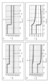
- FIG. 5A and 5B are diagrams for explaining an example of an output result of an inverter in the voltage control device according to the embodiment.
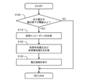
- 5 is a flowchart showing an example of processing by a control device in a voltage control device according to an embodiment.
- FIG. 1 is a diagram for explaining an overview of a power conversion system 1.
- the power conversion system 1 includes a voltage control device 10, a transformer 20, and a power system 30.
- the voltage control device 10 includes a battery 11, an inverter 12, and a control device 100.
- the inverter 12 is a device that converts the DC power output from the battery 11 into AC power and supplies the AC power to the power grid 30 via the transformer 20.
- An example of the inverter 12 is a voltage-controlled GFM inverter.
- the control device 100 is connected to the inverter 12 and controls the output power output from the inverter 12. Specifically, the control device 100 receives a detection value of the output voltage Vs (hereinafter referred to as the Vs detection value) and a detection value of the output current Io (hereinafter referred to as the Io detection value) output from the inverter 12.
- the Vs detection value and the Io detection value are detected by a detector (not shown) provided between the voltage control device 10 and the power system 30.
- the Vs detection value and the Io detection value detected between the voltage control device 10 and the transformer 20 are input to the control device 100, but the Vs detection value and the Io detection value detected between the transformer 20 and the power system 30 may also be input.
- the detection value of the AC voltage of the power system 30 may be the Vs detection value.
- the detection value of the AC current of the power system 30 may be the Io detection value.
- the output voltage Vs output from the inverter 12 is composed of three-phase voltages (Vsu, Vsv, Vsw), and the output current Io output from the inverter 12 is composed of three-phase currents (Iou, Iov, Iow).
- Vs detection value includes the Vsu detection value, the Vsv detection value, and the Vsw detection value
- Io detection value includes the Iou detection value, the Iov detection value, and the Iow detection value.
- the control device 100 executes VSG (Virtual Synchronous Generator) control based on the input Vs detection value and Io detection value.
- VSG is a virtual synchronous generator that simulates the dynamic characteristics of a synchronous generator in the inverter 12.
- VSG control means controlling a virtual synchronous generator.
- the dynamic characteristics of a synchronous generator include an inertia constant M, a braking constant D, etc. This makes it possible to prevent the power system 30 from becoming unstable when a system accident occurs, i.e., when a LVRT (Low Voltage Ride Through) occurs.
- the control device 100 performs voltage control on the inverter 12 so that the output current Io output from the inverter 12 becomes the current value required by the power grid 30 when LVRT occurs.
- the voltage control includes the generation of three-phase voltages (Vsu, Vsv, Vsw) and PWM control that performs pulse width modulation on each of the three-phase voltages.
- the control device 100 then outputs a voltage control signal generated by the PWM control to the inverter 12. This allows the inverter 12 to reduce the difference in AC power between the power grid 30 and the inverter 12 based on the voltage control signal.
- control device 100 has hardware that realizes various functions.
- the hardware may be a processing circuit, or a computer that executes a program stored in a storage device using a CPU.
- Examples of the processing circuit include an FPGA (Field Programmable Gate Array) and an ASIC (Application Specific Integrated Circuit).
- the control device 100 includes an effective reactive voltage calculation processing unit 101, an effective reactive current calculation processing unit 102, a VSG control unit 103, a dq-axis voltage conversion unit 104, a dq-axis current command calculation unit 105, a virtual impedance generation unit 106, a virtual voltage generation unit 107, a first output selection circuit 108, a second output selection circuit 109, a switching determination circuit 110, an addition/subtraction circuit 111, and a voltage control circuit 112.
- the effective and reactive voltage calculation processing unit 101 calculates the effective voltage Vd and the reactive voltage Vq based on the Vs detection value input to the control device 100.
- the effective voltage Vd and the reactive voltage Vq calculated by the effective and reactive voltage calculation processing unit 101 are expressed by the following formula (1), as an example.
- the active and reactive current calculation processing unit 102 calculates the active current Id and the reactive current Iq based on the Io detection value input to the control device 100.
- the active current Id and the reactive current Iq calculated by the active and reactive current calculation processing unit 102 are expressed, for example, by the following formula (2).
- the VSG control unit 103 generates a voltage command value Vref for the output voltage Vs of the inverter 12.
- the voltage command value Vref is a fixed value determined, for example, according to the power system 30 connected to the inverter 12.
- the voltage command value Vref includes a d-axis voltage command value Vdref and a q-axis voltage command value Vqref.
- the d-axis voltage command value Vdref is also called the effective voltage command value Vdref
- the q-axis voltage command value Vqref is also called the reactive voltage command value Vqref.
- the dq-axis voltage conversion unit 104 converts the voltage command value Vref generated by the VSG control unit 103 into the effective voltage command value Vdref and the reactive voltage command value Vqref.
- the dq-axis current command calculation unit 105 calculates the d-axis current command value Idref and the q-axis current command value Iqref required for the power system 30 based on the voltage command value Vref and the Vs detection value.
- the d-axis current command value Idref is also called the active current command value Idref
- the d-axis current command value Idref is also called the reactive current command value Iqref.
- the active current command value Idref and the reactive current command value Iqref calculated by the dq-axis current command calculation unit 105 are expressed by the following formulas (3) and (4), respectively, as an example.
- k is a constant value determined by the specifications of the inverter 12.
- ⁇ V is the differential voltage Vdiff obtained by subtracting the voltage command value Vref from the Vs detection value.
- the reactive current command value Iqref is calculated so that the sum of the squared value of the active current command value Idref and the squared value of the reactive current command value Iqref is 1. Therefore, when the active current command value Idref is 80%, the reactive current command value Iqref is 60% according to formula (4).
- the virtual impedance generating unit 106 calculates a virtual impedance to increase the output voltage Vs of the inverter 12.
- the virtual impedance includes a resistance Rv and a reactance Xv.
- the resistance Rv and the reactance Xv are calculated based on the active voltage command value Vdref, the reactive voltage command value Vqref, the active current command value Idref, the reactive current command value Iqref, the active voltage Vd, and the reactive voltage Vq, respectively.
- the calculation of the virtual impedance (resistance Rv and reactance Xv) will be described in detail later.
- the virtual voltage generating unit 107 generates a virtual effective voltage Vud and a virtual reactive voltage Vuq for increasing the output voltage Vs of the inverter 12 based on the virtual impedance (resistance Rv and reactance Xv), the active current Id, and the reactive current Iq.
- the virtual effective voltage Vud and the virtual voltage Vuq calculated by the virtual voltage generating unit 107 are each expressed by the following equation (5), as an example.
- the first output selection circuit 108 is a changeover switch having two input terminals and one output terminal.
- the first output selection circuit 108 switches to select one of the two input terminals. Specifically, when the switching determination result input to the first output selection circuit 108 is "0", the first output selection circuit 108 switches to select the first input terminal. On the other hand, when the switching determination result input to the first output selection circuit 108 is "1", the first output selection circuit 108 switches to select the second input terminal.
- a fixed value (a value of zero) is input to the first input terminal of the first output selection circuit 108, and a virtual effective voltage Vud is input to the second input terminal of the first output selection circuit 108.
- the switching judgment result is generated by the switching judgment circuit 110.
- the switching judgment circuit 110 When the differential voltage Vdiff between the Vs detection value and the voltage command value Vref is less than the threshold value, i.e., when the AC voltage of the power system 30 is not in the LVRT state, the switching judgment circuit 110 outputs "0" as the switching judgment result.
- the switching judgment circuit 110 when the differential voltage Vdiff between the Vs detection value and the voltage command value Vref is equal to or greater than the threshold value, i.e., when the AC voltage of the power system 30 is in the LVRT state, the switching judgment circuit 110 outputs "1" as the switching judgment result.
- the first output selection circuit 108 outputs the voltage input to the selected input terminal. The voltage output from the first output selection circuit 108 is called the selected effective voltage Vdsel.
- the second output selection circuit 109 is a changeover switch having two input terminals and one output terminal.
- the second output selection circuit 109 switches to select one of the two input terminals. Specifically, when the switching determination result input to the second output selection circuit 109 is "0", the second output selection circuit 109 switches to select the first input terminal. On the other hand, when the switching determination result input to the second output selection circuit 109 is "1", the second output selection circuit 109 switches to select the second input terminal.
- a fixed value (a value of zero) is input to the first input terminal of the second output selection circuit 109, and a virtual reactive voltage Vuq is input to the second input terminal of the second output selection circuit 109.
- the switching determination result is generated by the switching determination circuit 110 as described above.
- the second output selection circuit 109 outputs the voltage input to the selected input terminal.
- the voltage output from the second output selection circuit 109 is called the selected reactive voltage Vqsel.
- the addition/subtraction circuit 111 includes four addition/subtraction circuits (first addition/subtraction circuit 111a, second addition/subtraction circuit 111b, third addition/subtraction circuit 111c, and fourth addition/subtraction circuit 111d).
- the first addition/subtraction circuit 111a is an addition/subtraction circuit that adds an active voltage command value Vdref and subtracts a selected active voltage Vdsel.
- the second addition/subtraction circuit 111b is an addition/subtraction circuit that adds a reactive voltage command value Vqref and subtracts a selected reactive voltage Vqsel.
- the third addition/subtraction circuit 111c is an addition/subtraction circuit that adds the output of the first addition/subtraction circuit 111a and subtracts an active voltage Vd.
- the fourth addition/subtraction circuit 111d is an addition/subtraction circuit that adds the output of the second addition/subtraction circuit 111b and subtracts a reactive voltage Vq.
- equation (5) is substituted into equation (6), it is expressed as the following equation (7).
- the power factor which is the percentage of the effective voltage Vd relative to the output voltage Vs of the inverter 12 is high.
- the voltage control device 10 can output appropriate active current Id and reactive current Iq to the power grid 30.
- the voltage control circuit 112 is a circuit that controls the voltage based on the virtual effective voltage Vud and virtual reactive voltage Vuq calculated based on the virtual impedance so that the active current Id and reactive current Iq approach the active current command value Idref and reactive current command value Iqref, respectively, required by the power system 30.
- the voltage control circuit 112 then outputs a voltage control signal Vsc generated by the voltage control.
- voltage control includes the process of generating three-phase voltages (Vsu, Vsv, Vsw) and PWM control, which performs pulse width modulation on each of the three-phase voltages.
- PWM control the generated three-phase voltages are controlled to have a predetermined pulse width and a predetermined frequency.
- PI control for example, is used to generate the three-phase voltages by voltage control.
- FIG. 3 is an explanatory diagram showing a specific example of the virtual impedance of the voltage control device 10 according to the embodiment. Specifically, Fig. 3 shows the waveforms of resistance Rv and reactance Xv in the virtual impedance with respect to the Vs detection value. The horizontal axis of the graph shown in Fig. 3 indicates the Vs detection value, and the vertical axis indicates the values of resistance Rv and reactance Xv. In the example shown in Fig. 3, the value of each variable is expressed in PU (Per Unit), but may be expressed as a percentage.
- PU Per Unit
- the waveforms of the resistance Rv and reactance Xv are those obtained when the active voltage command value Vdref is set to "1" and the constant k is set to "2" in the above-mentioned equation (7).
- the active current command value Idref required for the power system 30 is 0% based on the above-mentioned equation (3)
- the reactive current command value Iqref required for the power system 30 is 100% based on the above-mentioned equation (4).
- the resistance Rv is 0.06 and the reactance Xv is 0.6, as shown in FIG. 3.
- FIG. 4 is a diagram for explaining an example of an output result of the inverter 12 in the voltage control device 10 according to the embodiment.
- FIG. 4(A) shows an example of the waveform of the active voltage Vd and the waveform of the reactive voltage Vq when the Vs detection value drops to 65%.
- FIG. 4(B) shows an example of the waveform of the active current Id and the reactive current Iq output from the inverter 12 to the power system 30 based on the voltage control signal Vsc generated by the voltage control circuit 112 when the Vs detection value drops to 65%.
- the active current Id is output at about 70% and the reactive current Iq is output at about -70%.
- Figure 4(C) shows an example of the waveform of the active voltage Vd and the waveform of the reactive voltage Vq when the Vs detection value has dropped to 40%.
- Figure 4(D) shows an example of the waveform of the active current Id and the reactive current Iq output from the inverter 12 to the power system 30 based on the voltage control signal Vsc generated by the voltage control circuit 112 when the Vs detection value has dropped to 40%.
- the active current Id is output at approximately 0% and the reactive current Iq is output at approximately -100%.
- the active current Id and reactive current Iq required by the power grid 30 are output based on the virtual impedance so as to reduce the difference in AC power between the power grid 30 and the inverter 12.
- Processing Example Fig. 5 is a flowchart showing a processing example of the control device 100 in the voltage control device 10 according to the embodiment.
- step S100 the control device 100 determines whether the voltage drop in the output voltage of the inverter 12 is equal to or greater than a threshold value. If the voltage drop in the output voltage is equal to or greater than the threshold value (step S100; Yes), the process proceeds to step S110. Otherwise (step S100; No), the control device 100 ends the process.
- step S110 the control device 100 calculates the virtual impedance based on the voltage command value Vref and the output voltage Vs of the inverter 12. Then, the process proceeds to step S120.
- the virtual impedance is calculated based on a predetermined condition.
- the predetermined condition means a condition in which the reactive voltage Vq is zero, the reactive voltage command value Vqref is zero, the voltage value obtained by subtracting the virtual effective voltage Vud and the effective voltage Vd from the effective voltage command value Vdref is zero, and the voltage value obtained by subtracting the virtual reactive voltage Vuq and the reactive voltage Vq from the reactive voltage command value Vqref is zero.
- step S120 the control device 100 calculates the virtual effective voltage Vud and the virtual reactive voltage Vuq by multiplying the active current Id and the reactive current Iq, which are calculated based on the output current Io of the inverter 12, by the virtual impedance. Then, the process proceeds to step S130.
- step S130 the control device 100 performs voltage control based on the virtual effective voltage Vud and the virtual reactive voltage Vuq so that the active current Id and the reactive current Iq output from the inverter 12 approach the active current command value Idref and the reactive current command value Iqref, respectively, required by the power system 30.
- a virtual impedance is calculated based on the voltage command value Vref and the output voltage Vs of the inverter 12. Then, in the voltage control device 10, a virtual effective voltage Vud and a virtual reactive voltage Vuq are generated based on the virtual impedance.
- voltage control is performed based on the virtual effective voltage Vud and the virtual reactive voltage Vuq so that the active current Id and the reactive current Iq output from the inverter 12 approach the active current command value Idref and the reactive current command value Iqref required by the power system 30, respectively.
- the active current Id and the reactive current Iq required by the power system 30 can be output. Therefore, it is possible to stabilize the power system 30.
- 1...power conversion system 10...voltage control device, 11...battery, 12...inverter, 20...transformer, 30...power system, 100...control device, 101...effective and reactive voltage calculation processing unit, 102...effective and reactive current calculation processing unit, 103...VSG control unit, 104...dq-axis voltage conversion unit, 105...dq-axis current command calculation unit, 106...virtual impedance generation unit, 107...virtual voltage generation unit, 108...first output selection circuit, 109...second output selection circuit, 110...switching determination circuit, 111...addition and subtraction circuit, 111a...first addition and subtraction circuit, 111b...second addition and subtraction circuit, 111c...third addition and subtraction circuit, 111d...fourth addition and subtraction circuit, 112...voltage control circuit
Landscapes
- Engineering & Computer Science (AREA)
- Power Engineering (AREA)
- Inverter Devices (AREA)
Priority Applications (5)
| Application Number | Priority Date | Filing Date | Title |
|---|---|---|---|
| PCT/JP2023/024459 WO2025004355A1 (ja) | 2023-06-30 | 2023-06-30 | 電圧制御装置及び電圧制御方法 |
| CN202380052039.5A CN119563280A (zh) | 2023-06-30 | 2023-06-30 | 电压控制装置以及电压控制方法 |
| US18/995,374 US20260039115A1 (en) | 2023-06-30 | 2023-06-30 | Voltage control apparatus and voltage control method |
| EP23943743.7A EP4738680A1 (en) | 2023-06-30 | 2023-06-30 | Voltage control apparatus and voltage control method |
| JP2025529381A JPWO2025004355A1 (https=) | 2023-06-30 | 2023-06-30 |
Applications Claiming Priority (1)
| Application Number | Priority Date | Filing Date | Title |
|---|---|---|---|
| PCT/JP2023/024459 WO2025004355A1 (ja) | 2023-06-30 | 2023-06-30 | 電圧制御装置及び電圧制御方法 |
Publications (1)
| Publication Number | Publication Date |
|---|---|
| WO2025004355A1 true WO2025004355A1 (ja) | 2025-01-02 |
Family
ID=93938038
Family Applications (1)
| Application Number | Title | Priority Date | Filing Date |
|---|---|---|---|
| PCT/JP2023/024459 Ceased WO2025004355A1 (ja) | 2023-06-30 | 2023-06-30 | 電圧制御装置及び電圧制御方法 |
Country Status (5)
| Country | Link |
|---|---|
| US (1) | US20260039115A1 (https=) |
| EP (1) | EP4738680A1 (https=) |
| JP (1) | JPWO2025004355A1 (https=) |
| CN (1) | CN119563280A (https=) |
| WO (1) | WO2025004355A1 (https=) |
Citations (3)
| Publication number | Priority date | Publication date | Assignee | Title |
|---|---|---|---|---|
| JP2012085500A (ja) * | 2010-10-15 | 2012-04-26 | Mitsubishi Electric Corp | 無効電力補償装置 |
| WO2021029313A1 (ja) * | 2019-08-09 | 2021-02-18 | 東京電力ホールディングス株式会社 | 系統連系電力変換装置 |
| JP7183486B1 (ja) * | 2022-05-30 | 2022-12-05 | 三菱電機株式会社 | 電力変換装置、および制御装置 |
-
2023
- 2023-06-30 CN CN202380052039.5A patent/CN119563280A/zh active Pending
- 2023-06-30 US US18/995,374 patent/US20260039115A1/en active Pending
- 2023-06-30 EP EP23943743.7A patent/EP4738680A1/en active Pending
- 2023-06-30 JP JP2025529381A patent/JPWO2025004355A1/ja active Pending
- 2023-06-30 WO PCT/JP2023/024459 patent/WO2025004355A1/ja not_active Ceased
Patent Citations (3)
| Publication number | Priority date | Publication date | Assignee | Title |
|---|---|---|---|---|
| JP2012085500A (ja) * | 2010-10-15 | 2012-04-26 | Mitsubishi Electric Corp | 無効電力補償装置 |
| WO2021029313A1 (ja) * | 2019-08-09 | 2021-02-18 | 東京電力ホールディングス株式会社 | 系統連系電力変換装置 |
| JP7183486B1 (ja) * | 2022-05-30 | 2022-12-05 | 三菱電機株式会社 | 電力変換装置、および制御装置 |
Also Published As
| Publication number | Publication date |
|---|---|
| JPWO2025004355A1 (https=) | 2025-01-02 |
| CN119563280A (zh) | 2025-03-04 |
| EP4738680A1 (en) | 2026-05-06 |
| US20260039115A1 (en) | 2026-02-05 |
Similar Documents
| Publication | Publication Date | Title |
|---|---|---|
| JP6739649B2 (ja) | 電力変換装置および電力変換システム | |
| EP3148067B1 (en) | Direct-current power transmission power conversion device and direct-current power transmission power conversion method | |
| KR101699174B1 (ko) | 마이크로그리드용 인버터 장치 및 이를 제어하는 방법 | |
| CN109617082B (zh) | 一种抑制微电网电压频率越限的暂态稳定控制方法 | |
| JP2018129963A (ja) | 電力変換器の制御装置 | |
| JP2016111810A (ja) | インバータ回路を制御する制御回路、および、当該制御回路を備えたインバータ装置 | |
| JP6771707B1 (ja) | 電力変換装置 | |
| JP2014192992A (ja) | 無効電力比率制御器、無効電力比率制御方法、およびこれを用いた発電システム | |
| WO2025004355A1 (ja) | 電圧制御装置及び電圧制御方法 | |
| WO2025004340A1 (ja) | 電圧制御装置及び電圧制御方法 | |
| Guo et al. | A Sensorless Current Feedforward Method for Single-Phase AC–DC Converter | |
| JP2017153277A (ja) | 自励式無効電力補償装置 | |
| KR102691036B1 (ko) | 전력 변환 장치의 전력 제어 시스템 및 방법 | |
| Hazem et al. | Performance and control of a back to back MMC-HVDC for asynchronous ac networks interconnection | |
| CN118117610A (zh) | 风力发电系统的控制方法及风力发电系统 | |
| CN109039097B (zh) | 变频控制方法、装置、岸电系统和存储介质 | |
| JP3374827B2 (ja) | 無効電力発生装置 | |
| US20250274054A1 (en) | Power conversion device | |
| WO2026048044A1 (ja) | パワーコンディショナ | |
| JP7495654B1 (ja) | 電力変換器制御装置、電力変換器の制御方法及び電力変換器の制御プログラム | |
| JP6980134B1 (ja) | 電力変換装置、電力変換制御装置、及び制御方法 | |
| Insfran et al. | Reactive Power Compensation Model in A Three-Level NPC Topology Using Sequential Predictive Current Control with Space Vector Pulse Width Modulation | |
| Meetei et al. | A non-singular terminal sliding mode controls base voltage and frequency control in an islanded microgrid | |
| KR101750224B1 (ko) | 인버터의 절체 제어 장치 및 그 방법 | |
| Kouki et al. | Design and Implementation of Robust Control for Three-Phase Active Rectifier |
Legal Events
| Date | Code | Title | Description |
|---|---|---|---|
| WWE | Wipo information: entry into national phase |
Ref document number: 202380052039.5 Country of ref document: CN |
|
| WWE | Wipo information: entry into national phase |
Ref document number: 202517001592 Country of ref document: IN |
|
| WWE | Wipo information: entry into national phase |
Ref document number: 18995374 Country of ref document: US |
|
| 121 | Ep: the epo has been informed by wipo that ep was designated in this application |
Ref document number: 23943743 Country of ref document: EP Kind code of ref document: A1 |
|
| WWP | Wipo information: published in national office |
Ref document number: 202517001592 Country of ref document: IN |
|
| WWE | Wipo information: entry into national phase |
Ref document number: 2025529381 Country of ref document: JP |
|
| WWP | Wipo information: published in national office |
Ref document number: 202380052039.5 Country of ref document: CN |
|
| WWE | Wipo information: entry into national phase |
Ref document number: 2023943743 Country of ref document: EP |
|
| NENP | Non-entry into the national phase |
Ref country code: DE |
|
| ENP | Entry into the national phase |
Ref document number: 2023943743 Country of ref document: EP Effective date: 20260130 |
|
| WWP | Wipo information: published in national office |
Ref document number: 18995374 Country of ref document: US |
|
| ENP | Entry into the national phase |
Ref document number: 2023943743 Country of ref document: EP Effective date: 20260130 |