WO2025004207A1 - 空間光変調素子、光学ユニット、及び光加工装置 - Google Patents
空間光変調素子、光学ユニット、及び光加工装置 Download PDFInfo
- Publication number
- WO2025004207A1 WO2025004207A1 PCT/JP2023/023921 JP2023023921W WO2025004207A1 WO 2025004207 A1 WO2025004207 A1 WO 2025004207A1 JP 2023023921 W JP2023023921 W JP 2023023921W WO 2025004207 A1 WO2025004207 A1 WO 2025004207A1
- Authority
- WO
- WIPO (PCT)
- Prior art keywords
- positive
- modulation element
- region
- spatial light
- light
- Prior art date
- Legal status (The legal status is an assumption and is not a legal conclusion. Google has not performed a legal analysis and makes no representation as to the accuracy of the status listed.)
- Ceased
Links
Images











Classifications
-
- G—PHYSICS
- G02—OPTICS
- G02F—OPTICAL DEVICES OR ARRANGEMENTS FOR THE CONTROL OF LIGHT BY MODIFICATION OF THE OPTICAL PROPERTIES OF THE MEDIA OF THE ELEMENTS INVOLVED THEREIN; NON-LINEAR OPTICS; FREQUENCY-CHANGING OF LIGHT; OPTICAL LOGIC ELEMENTS; OPTICAL ANALOGUE/DIGITAL CONVERTERS
- G02F1/00—Devices or arrangements for the control of the intensity, colour, phase, polarisation or direction of light arriving from an independent light source, e.g. switching, gating or modulating; Non-linear optics
- G02F1/01—Devices or arrangements for the control of the intensity, colour, phase, polarisation or direction of light arriving from an independent light source, e.g. switching, gating or modulating; Non-linear optics for the control of the intensity, phase, polarisation or colour
- G02F1/015—Devices or arrangements for the control of the intensity, colour, phase, polarisation or direction of light arriving from an independent light source, e.g. switching, gating or modulating; Non-linear optics for the control of the intensity, phase, polarisation or colour based on semiconductor elements having potential barriers, e.g. having a PN or PIN junction
- G02F1/0151—Devices or arrangements for the control of the intensity, colour, phase, polarisation or direction of light arriving from an independent light source, e.g. switching, gating or modulating; Non-linear optics for the control of the intensity, phase, polarisation or colour based on semiconductor elements having potential barriers, e.g. having a PN or PIN junction modulating the refractive index
-
- G—PHYSICS
- G02—OPTICS
- G02F—OPTICAL DEVICES OR ARRANGEMENTS FOR THE CONTROL OF LIGHT BY MODIFICATION OF THE OPTICAL PROPERTIES OF THE MEDIA OF THE ELEMENTS INVOLVED THEREIN; NON-LINEAR OPTICS; FREQUENCY-CHANGING OF LIGHT; OPTICAL LOGIC ELEMENTS; OPTICAL ANALOGUE/DIGITAL CONVERTERS
- G02F2203/00—Function characteristic
- G02F2203/12—Function characteristic spatial light modulator
Definitions
- the present invention relates to a spatial light modulation element, an optical unit, and an optical processing device.
- Known electro-optic spatial light modulation elements include a spatial light modulation element in which an electrode is provided on one side of an optical member that propagates light (see, for example, Patent Document 1), and a spatial light modulation element in which electrodes are provided on both sides of an optical member that propagates light. Such spatial light modulation elements are required to modulate light at high speed.
- the spatial light modulation element is a spatial light modulation element that modulates and emits incident light, and includes an optical element on which the incident light traveling along a first axis is incident and which is formed using a translucent ferroelectric material, first and second electrodes that are arranged on the surface of the optical element along a second axis that intersects with the first axis, and wiring that applies a voltage to at least one of the first and second electrodes so as to create a potential difference between the first and second electrodes.
- the second spatial light modulation element is a spatial light modulation element that modulates and emits incident light, and includes an optical element on which the incident light traveling along a first axis is incident and is formed using a translucent ferroelectric material, and first and second electrodes that are arranged on the surface of the optical element along a second axis that intersects with the first axis, and when a potential difference is generated between the first and second electrodes, the refractive index within the optical element changes along the second axis.
- the optical unit according to the present invention comprises the spatial light modulation element described above and an optical system into which the diffracted light emitted from the spatial light modulation element is incident, and the optical system has a light-attenuating section that attenuates at least one of the zeroth-order diffracted light in the diffracted light and the diffracted light of an order different from the zeroth-order diffracted light.
- the optical processing device is an optical processing device that processes an object using processing light from a light source, and includes the optical unit described above, and an irradiation device that irradiates the object with the processing light from the light source via the optical unit.
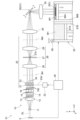
- FIG. 2 is a schematic configuration diagram showing an optical processing device.
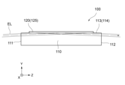
- FIG. 2 is a cross-sectional view showing a part of the optical processing apparatus.
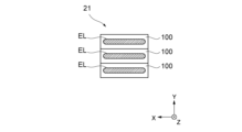
- 2 is a schematic diagram of a spatial light modulation element unit as viewed from the incident surface side.
- FIG. FIG. 13 is a schematic configuration diagram showing a first modified example of the optical processing apparatus.
- FIG. 13 is a schematic configuration diagram showing a second modified example of the optical processing apparatus.
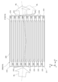
- 1 is a plan view of a spatial light modulation element according to a first embodiment.
- 2 is a plan view showing a state in which processing light is incident on the spatial light modulation element according to the first embodiment.
- FIG. 1 is a side view of a spatial light modulation element according to a first embodiment.
- FIG. 1 is a cross-sectional view of a spatial light modulation element according to a first embodiment.
- FIG. 1 is a plan view of a conventional spatial light modulation element.
- FIG. 1 is a side view of a conventional spatial light modulation element.
- FIG. 1 is a cross-sectional view of a conventional spatial light modulation element.
- FIG. 11 is a cross-sectional view showing a case where the distance between electrodes is narrowed in a conventional spatial light modulation element.
- FIG. 11 is a cross-sectional view showing a case where the distance between electrodes is increased in a conventional spatial light modulation element.
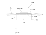
- FIG. 2 is a side view showing a first modified example of the spatial light modulation element according to the first embodiment.
- FIG. 1 is a plan view of a conventional spatial light modulation element.
- FIG. 1 is a side view of a conventional spatial light modulation element.
- FIG. 1 is a cross-sectional view of a conventional spatial light modulation element.
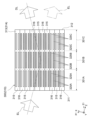
- FIG. 11 is a plan view of a spatial light modulation element according to a second embodiment.
- 13 is a plan view showing a state in which processing light is incident on a spatial light modulation element according to a second embodiment.
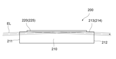
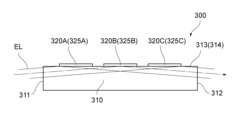
- FIG. 11 is a side view of a spatial light modulation element according to a second embodiment.
- FIG. 11 is a cross-sectional view of a spatial light modulation element according to a second embodiment.
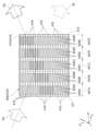
- FIG. 13 is a plan view of a spatial light modulation element according to a third embodiment.
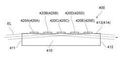
- FIG. 13 is a side view of a spatial light modulation element according to a third embodiment.
- FIG. 11 is a side view of a spatial light modulation element according to a third embodiment.
- FIG. 13 is a plan view showing a modified example of the spatial light modulation element according to the third embodiment.
- FIG. 13 is a plan view of a spatial light modulation element according to a fourth embodiment.
- FIG. 13 is a side view of a spatial light modulation element according to a fourth embodiment.
- FIG. 13 is a plan view showing a modified example of the spatial light modulation element according to the fourth embodiment.
- FIG. 13 is a plan view of a spatial light modulation element according to a fifth embodiment.
- FIG. 13 is a plan view of a spatial light modulation element according to a sixth embodiment.
- Figs. 1 to 4 the directions indicated by the arrows in Fig. 1 may be referred to as the X direction, Y direction, and Z direction, respectively.
- the X direction, Y direction, and Z direction are mutually orthogonal.
- the optical processing device 1 includes a light source 5, a processing optical system 10, an irradiation device 30, and a control device 40.
- the optical processing device 1 performs removal processing on the workpiece W1 by irradiating the workpiece W1 placed at a predetermined position (e.g., the upper surface of a stage ST) with processing light EL.
- the light source 5 emits processing light EL, such as laser light.
- the light source 5 may be a laser light source that emits pulsed light as the processing light EL.
- the pulsed light may be pulsed light also known as femtosecond laser.
- the processing light EL may be a type of light different from laser light, as long as it is capable of processing the workpiece W1 when irradiated onto the workpiece W1.
- the wavelength range of the processing light EL may be any wavelength range, as long as it is capable of processing the workpiece W1 when irradiated onto the workpiece W1.
- the wavelength range of the processing light EL may be the wavelength range of visible light, the wavelength range of infrared light, or the wavelength range of ultraviolet light.
- the processing light EL emitted from the light source 5 enters the processing optical system 10.
- the processing optical system 10 splits the processing light EL entering the processing optical system 10 into multiple processing lights (for example, nine processing lights arranged in threes vertically and threes horizontally) and emits them toward the irradiation device 30.
- the multiple processing lights EL emitted from the processing optical system 10 are irradiated onto the workpiece W1 via the galvanometer mirror 31 and scanning optical system 35 of the irradiation device 30.
- the direction along the optical axis of the processing optical system 10 is the Z direction.
- the horizontal direction perpendicular to the Z direction may be the X direction
- the direction perpendicular to the Z direction and the X direction may be the Y direction.
- the processing optical system 10 includes, in order from the light source 5 side, a diffractive optical element 11, a collector lens 12, a collimator lens 13, an optical isolator 14, a cylindrical expander 15, a cylindrical lens 16, an optical unit 20 having a spatial light modulation function, and a condenser lens 29.
- Processing light EL emitted from the light source 5 is incident on the diffractive optical element 11.
- the diffractive optical element 11 splits the processing light EL incident on the diffractive optical element 11 into multiple processing lights by the diffraction phenomenon. In the example shown in FIG.
- the diffractive optical element 11 splits the processing light EL incident on the diffractive optical element 11 into processing light EL that proceeds along the optical axis of the processing optical system 10 and two processing lights EL that proceed at an inclination in the ⁇ Y direction with respect to the optical axis of the processing optical system 10.
- the diffractive optical element 11 splits the processing light EL incident on the diffractive optical element 11 into three processing lights, but this is not limited to this.
- the diffractive optical element 11 may split the processing light EL incident on the diffractive optical element 11 into five processing lights, and it is sufficient if the diffractive optical element 11 can split the processing light EL incident on the diffractive optical element 11 into two or more processing lights.
- the multiple processed light beams EL emitted from the diffractive optical element 11 are incident on the collector lens 12.
- the front focal position of the collector lens 12 may be located on the grating surface of the diffractive optical element 11.
- the collector lens 12 makes the directions of travel of the multiple processed light beams EL passing through the collector lens 12 parallel to each other.
- the collector lens 12 also focuses each processed light beam EL passing through the collector lens 12.
- the collimator lenses 13 are aligned in the Y direction in positional alignment with the multiple processing light beams EL. As shown in FIG. 1, when the diffractive optical element 11 splits the processing light beam EL into three beams, three collimator lenses 13 may be aligned in the Y direction.
- the multiple collimator lenses 13 are incident with the multiple processing light beams EL that have passed through the collector lens 12.
- the collimator lenses 13 convert the processing light beams EL that pass through the collector lens 12 into parallel beams.
- the multiple beams of processing light EL that have passed through the multiple collimator lenses 13 are incident on the optical isolator 14.
- the optical isolator 14 transmits the multiple beams of processing light EL that have entered the optical isolator 14 from the multiple collimator lenses 13.
- the optical isolator 14 blocks the processing light EL that has been reflected by the workpiece W1.
- the cylindrical expanders 15 are aligned in the Y direction in positional alignment with the collimator lenses 13. As shown in FIG. 1, when the diffractive optical element 11 splits the processing light EL into three beams, three cylindrical expanders 15 may be aligned in the Y direction.
- the processing light EL that has passed through the optical isolator 14 is incident on the cylindrical expanders 15.
- the cylindrical expanders 15 expand the width of the processing light EL that passes through the cylindrical expanders 15 in the X direction (see FIG. 2).
- the multiple processed light beams EL that have passed through the multiple cylindrical expanders 15 are incident on the cylindrical lens 16.
- the cylindrical lens 16 focuses each processed light beam EL that passes through the cylindrical lens 16 in the Y direction.
- the cross-sectional shape of the processed light beam EL that enters the spatial light modulator 100 of the optical unit 20 becomes an ellipse whose width in the Y direction is smaller than its width in the X direction (see FIG. 3).
- the processed light beam EL that has an elliptical cross-sectional shape that enters the spatial light modulator 100 may be referred to as a sheet-shaped processed light beam EL.
- the cylindrical expanders 15 and cylindrical lenses 16 that shape the beam cross-sectional shape of the processed light beam EL from the light source 5 into an ellipse may be referred to as a shaping optical system.
- the optical unit 20 is irradiated with a plurality of processed light beams EL that have passed through the cylindrical lens 16.
- the optical unit 20 includes a spatial light modulation element unit 21, a lens array 23, and a Schlieren optical system 25, which are arranged in order from the light source 5 side.
- the spatial light modulation element unit 21 includes a plurality of spatial light modulation elements 100 arranged in a stacked manner in the Y direction, and a driving circuit 22.
- the plurality of spatial light modulation elements 100 may be arranged at the rear focal position of the collector lens 12. As shown in FIG. 1, when the diffractive optical element 11 splits the processed light EL into three beams, the spatial light modulation element unit 21 may include three spatial light modulation elements 100 arranged in a stacked manner in the Y direction.
- the driving circuit 22 is electrically connected to a plurality of electrodes provided on the plurality of spatial light modulation elements 100 via wiring EW, and is capable of applying a voltage to each electrode of the spatial light modulation element 100.
- a plurality of processed light beams EL that have passed through the cylindrical lens 16 are incident on a plurality of spatial light modulation elements 100.
- the spatial light modulation element 100 emits the processed light EL that has entered the spatial light modulation element 100 as 0th order diffracted light toward the lens array 23.
- the processed light EL that has entered the spatial light modulation element 100 is diffracted to generate diffracted light of a predetermined order (for example, +1st order or -1st order).
- a voltage is applied to some of the electrodes of the spatial light modulation element 100, a portion of the processed light EL that has entered the spatial light modulation element 100 is diffracted to generate diffracted light of a predetermined order.
- the spatial light modulation element 100 when a voltage is applied to the electrode located at the center of the spatial light modulation element 100, the spatial light modulation element 100 emits a diffracted light DL of a predetermined order generated by the diffraction of the central portion of the processed light EL having an elliptical cross-sectional shape (sheet-like) that is incident on the spatial light modulation element 100 toward the lens array 23, as shown in FIG. 2, and emits the light of the other portion of the processed light EL (portions on the end sides in the ⁇ X direction) toward the lens array 23 as 0th-order diffracted light.
- the spatial light modulation element 100 when a voltage is applied to the electrode located at the end side of the spatial light modulation element 100 in the +X direction (or -X direction), the spatial light modulation element 100 emits a diffracted light of a predetermined order generated by the diffraction of the light of the end side of the processed light EL in the +X direction (or -X direction) of the processed light EL that is incident on the spatial light modulation element 100 toward the lens array 23, and emits the light of the other portion of the processed light EL toward the lens array 23 as 0th-order diffracted light.
- two diffracted lights DL are emitted from the spatial light modulation element 100 instead of the processed light EL (0th order diffracted light
- one diffracted light e.g., +1st order diffracted light or -1st order diffracted light
- the diffracted light of a specified order may be, for example, +1st order diffracted light or -1st order diffracted light, as long as it is a diffracted light of an order different from the 0th order diffracted light.
- the processed light EL or diffracted light DL emitted from the spatial light modulation elements 100 is incident on the lens array 23.
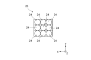
- the lens array 23 has a plurality of lenses 24 arranged in two directions, the X direction and the Y direction.
- Each lens 24 of the lens array 23 is generally composed of a lens (anamorphic lens) having different power in the X direction and the Y direction, and is aligned in the Y direction in alignment with the spatial light modulation elements 100.
- each lens 24 of the lens array 23 may be aligned in the Y direction in three in alignment with the three spatial light modulation elements 100.
- the lenses 24 of the lens array 23 are arranged in a row in the X direction within the range of the X-direction width of the spatial light modulation element 100.
- the lenses 24 of the lens array 23 are arranged in a row in the X direction in threes within the range of the X-direction width of the spatial light modulation element 100, and are aligned with the electrodes grouped into three control groups in the spatial light modulation element 100.
- the lens array 23 divides the processing light EL incident on the lens array 23 into three in the X direction and makes it incident on the Schlieren optical system 25. As shown in FIG.
- the lens array 23 makes the diffracted light DL incident on the lens array 23 incident on the Schlieren optical system 25. Note that in the example shown in FIG. 2, the processing light EL emitted from the lenses 24 on the ⁇ X-direction end sides of the lens array 23 is shown as a principal ray and marginal rays (upper ray and lower ray).
- the lenses 24 of the lens array 23 are arranged in groups of three in the X direction, but this is not limited to this.
- the lenses 24 of the lens array 23 may be arranged in groups of five in the X direction within the range of the X-direction width of the spatial light modulation element 100, or two or more in the X direction.
- the lenses 24 of the lens array 23 may be arranged in a single row in the X direction, that is, in a row in the Y direction.
- the position of the intermediate image located on the front focal plane of the Schlieren optical system 25 may be aligned with the position of the exit end of the spatial light modulation element 100 without providing the lens array 23.
- the Schlieren optical system 25 includes a first relay lens 26, an aperture 27, and a second relay lens 28, arranged in order from the light source 5 side.
- the first relay lens 26 receives the processed light EL or diffracted light DL that has passed through each lens 24 of the lens array 23.
- the first relay lens 26 collects the multiple processed light beams EL that have entered the first relay lens 26 toward the center of the aperture 27.
- the aperture 27 is disposed at the rear focal position of the first relay lens 26.
- An opening 27a is formed in the center of the aperture 27, through which the multiple processing lights EL that pass through the first relay lens 26 and converge can pass.
- the aperture 27 blocks the diffracted light DL from the spatial light modulation element unit 21 that passes through the first relay lens 26.
- the multiple processed light beams EL that have passed through the opening 27a of the diaphragm 27 are incident on the second relay lens 28.
- the second relay lens 28 makes the directions of travel of the multiple processed light beams EL that pass through the second relay lens 28 parallel to each other.
- the second relay lens 28 is positioned so that the front focal position of the second relay lens 28 is located at the rear focal position of the first relay lens 26.
- the multiple beams of processing light EL that have passed through the second relay lens 28 are incident on the focusing lens 29.
- the focusing lens 29 collects the multiple beams of processing light EL that have entered the focusing lens 29 toward the galvanometer mirror 31 of the irradiation device 30.
- the focusing lens 29 may be positioned so that the front focal position of the focusing lens 29 is located at the rear focal position of the second relay lens 28.
- the irradiation device 30 (galvanometer mirror 31) is incident on a plurality of processing lights EL that have passed through the focusing lens 29.
- the irradiation device 30 irradiates the plurality of processing lights EL that have entered the irradiation device 30 onto the workpiece W1.
- the irradiation device 30 includes a galvanometer mirror 31 and a scanning optical system 35, which are arranged in order from the light source 5 side.
- the galvanometer mirror 31 changes the emission direction of the multiple processing light beams EL by swinging or rotating the reflecting surface to change the angle relative to the optical path of the processing light EL.
- the change in the emission direction of the multiple processing light beams EL by the galvanometer mirror 31 is converted by the scanning optical system 35 into a change in the irradiation position of the multiple processing light beams EL. Therefore, by changing the emission direction of the multiple processing light beams EL by the galvanometer mirror 31, the irradiation position (focus position) of the processing light EL on the workpiece W1 can be changed. This allows the galvanometer mirror 31 to scan the surface of the workpiece W1 with the multiple processing light beams EL.
- a polygon scanner, an acousto-optical element, or the like may be used to scan the surface of the workpiece W1 with the multiple processing light beams EL.
- the processing light EL emitted from the galvanometer mirror 31 is incident on the scanning optical system 35.
- the scanning optical system 35 focuses the processing light EL from the galvanometer mirror 31 on the surface of the workpiece W1. In other words, the scanning optical system 35 irradiates the surface of the workpiece W1 with the processing light EL in a convergent state.
- the control device 40 is configured using, for example, a CPU (central processing unit) and a memory (not shown).
- the control device 40 controls the operation of the light source 5, the drive circuit 22, the galvanometer mirror 31, etc. based on a control program stored in the memory.
- the processing light EL emitted from the light source 5 enters the processing optical system 10.
- the processing optical system 10 splits the processing light EL entering the processing optical system 10 into multiple processing lights (for example, nine processing lights arranged in threes vertically and horizontally) and emits them toward the irradiation device 30.
- the multiple processing lights EL emitted from the processing optical system 10 are irradiated onto the workpiece W1 via the galvanometer mirror 31 and scanning optical system 35 of the irradiation device 30.
- the galvanometer mirror 31 changes the emission direction of the multiple processing lights EL, thereby changing the irradiation position (focus position) of the processing light EL relative to the workpiece W1.
- the galvanometer mirror 31 scans the surface of the workpiece W1 with the multiple processing lights EL.
- the multiple processing light beams EL emitted from the diffractive optical element 11 are incident on the collector lens 12.
- the multiple processing light beams EL that have passed through the collector lens 12 are incident on the multiple collimator lenses 13.
- the multiple processing light beams EL that have passed through the multiple collimator lenses 13 are incident on the optical isolator 14.
- the multiple processing light beams EL that have passed through the optical isolator 14 are incident on the multiple cylindrical expanders 15.
- the multiple processing light beams EL that have passed through the multiple cylindrical expanders 15 are incident on the cylindrical lenses 16.
- the multiple processing light beams EL that have passed through the cylindrical lenses 16 are incident on the multiple spatial light modulation elements 100 of the optical unit 20 (spatial light modulation element unit 21).
- the cross-sectional shape of the processing light beams EL that are incident on each spatial light modulation element 100 is an ellipse whose width in the Y direction is smaller than its width in the X direction (see FIG. 3).
- the processing light EL that is incident on the spatial light modulation element 100 is emitted from the spatial light modulation element 100 as zero-order diffracted light and enters the lens array 23.
- the processing light EL (for example, nine processing light EL arranged in threes in the X direction and Y direction) that is split after passing through each lens 24 of the lens array 23 is once focused at the focal position of the lens array 23 (position of the first intermediate image IM1) to form a plurality (nine) discrete focused beams.
- the processing light EL that is once focused at the focal position of the lens array 23 enters the first relay lens 26 of the Schlieren optical system 25.
- the processing light EL that is transmitted through the first relay lens 26 passes through the opening 27a of the diaphragm 27 and enters the second relay lens 28.
- the multiple processing lights EL that have passed through the second relay lens 28 are focused again at the rear focal position of the second relay lens 28 (the position of the second intermediate image IM2) to form multiple (nine) discrete focused beams.
- the multiple processing lights EL that have been focused again at the rear focal position of the second relay lens 28 are incident on the focusing lens 29.
- the multiple processing lights EL that have passed through the focusing lens 29 are collected by the galvanometer mirror 31 of the irradiation device 30.
- the processed light EL incident on the spatial light modulation element 100 is diffracted to generate diffracted light of a predetermined order.
- a voltage is applied to the electrodes of the control group corresponding to some of the lenses 24 of the lens array 23 in the spatial light modulation element 100, a part of the processed light EL incident on the spatial light modulation element 100 is diffracted to generate diffracted light of a predetermined order.
- the light of the central part of the processed light EL which has an elliptical cross-sectional shape (sheet-like) and is incident on the spatial light modulation element 100, is diffracted with a diffraction efficiency according to the applied voltage, and diffracted light DL of a predetermined order is emitted from the spatial light modulation element 100.
- a part of the light of the central part of the processed light EL is emitted from the spatial light modulation element 100 as 0th order diffracted light.
- the diffracted light DL emitted from the spatial light modulator 100 passes through the lens array 23 and travels at an incline in the X direction with respect to the optical axis of the processing optical system 10, and enters the first relay lens 26 of the Schlieren optical system 25.
- the diffracted light DL that travels at an incline with respect to the optical axis of the processing optical system 10 and passes through the first relay lens 26 is blocked by the aperture 27.
- the processing light EL is diffracted by the spatial light modulator 100 and reduced in intensity by the aperture 27.
- At least one of the multiple processing lights EL (for example, nine processing lights arranged in threes vertically and horizontally) can be selected so as not to be irradiated onto the workpiece W1 (when a voltage that provides a diffraction efficiency of 100% is applied to the electrodes).
- the intensity of some of the multiple processing lights EL can be changed continuously or stepwise to irradiate the workpiece W1.
- the drive circuit 22 with the control device 40 and changing which of the multiple electrodes provided on the multiple spatial light modulators 100 to which voltage is applied, it is possible to selectively change the processing light EL to be irradiated onto the workpiece W1 in a short period of time.
- the intensity of the processing light irradiated onto the workpiece W1 can also be changed continuously or stepwise. Therefore, with the optical processing device 1 equipped with the optical unit 20 (spatial light modulator 100), the shape of the processing light irradiated onto the workpiece W1 can be changed in a short period of time within the range in which the voltage can be controlled, making it possible to perform more diverse processing.
- a shaping optical system may also be provided to shape the cross-sectional beam shape of the processing light EL from the light source 5 into an elliptical shape. This allows the spatial light modulation element 100 to emit a diffracted light DL of a predetermined order that is generated by diffraction of a portion of the processing light EL having an elliptical cross-sectional shape that is incident on the spatial light modulation element 100, and emit the other portion of the processing light EL as zeroth-order diffracted light.
- the zeroth order diffracted light emitted from the spatial light modulation element 100 passes through the opening 27a of the aperture 27, and the diffracted light of a predetermined order emitted from the spatial light modulation element 100 is blocked by the aperture 27, but this is not limited to the above.
- the diffracted light of a predetermined order emitted from the spatial light modulation element 100 may pass through the opening 27a of the aperture 27, and the zeroth order diffracted light emitted from the spatial light modulation element 100 may be blocked by the aperture 27.
- a neutral density filter having an opening in the center may be provided so that the amount of diffracted light is significantly reduced by the neutral density filter.
- the aperture 27 that blocks the diffracted light and the neutral density filter that reduces the amount of diffracted light can also be said to be a neutral density section that reduces the diffracted light.
- the Schlieren optical system 25 between the lens array 23 and the condenser lens 29 may be omitted.
- a light-attenuating section that attenuates the diffracted light of a predetermined order emitted from the spatial light modulation element 100 may be provided on the galvanometer mirror 31 where the multiple processing lights EL are collected by the condenser lens 29.
- a galvanometer mirror having a reflecting surface of a size or shape that does not allow the diffracted light of a predetermined order emitted from the spatial light modulation element 100 to enter may be used.
- the optical processing device equipped with the spatial light modulator 100 is not limited to the optical processing device 1 that performs the above-mentioned removal processing, but may be an optical processing device 51 (see FIG. 5) that performs additional processing.
- the optical processing device 51 according to the first modification includes a light source 5, a processing optical system 10, an irradiation device 30, a control device 40, and a supply mechanism 55.
- the optical processing device 51 forms a three-dimensional object SC by irradiating the processing light EL onto the modeling material M1 supplied by the supply mechanism 55 and performing additional processing.
- the modeling material M1 is formed in a powder form using, for example, a metal material such as titanium or stainless steel, a resin material such as engineering plastic, a ceramic material, or the like.
- the light source 5, processing optical system 10, irradiation device 30, and control device 40 have the same configuration as the light source 5, processing optical system 10, irradiation device 30, and control device 40 of the optical processing device 1 described above, so the same reference numerals are used and detailed description is omitted.
- the light source 5 may be a laser light source that emits pulsed light as the processing light EL.
- the pulsed light may be pulsed light having a longer pulse width than that of a femtosecond laser.
- the wavelength of the processing light EL may be in the infrared wavelength range (e.g., 1064 nm).
- the supply mechanism 55 comprises a build piston 56A and a build cylinder 56B, a feed piston 57A and a feed cylinder 57B, and a leveling roller 58.
- the build piston 56A and the build cylinder 56B are arranged below the scanning optical system 35.
- the build piston 56A is attached inside the build cylinder 56B so as to be able to reciprocate in the vertical direction.
- the feed piston 57A and the feed cylinder 57B are arranged side by side to the sides of the build piston 56A and the build cylinder 56B.
- the feed piston 57A is arranged inside the feed cylinder 57B so as to be able to reciprocate in the vertical direction.
- the modeling material M1 is stored above the feed piston 57A inside the feed cylinder 57B.
- the leveling roller 58 is arranged so as to be able to reciprocate in an approximately horizontal direction between the upper edge of the feed cylinder 57B and the upper edge of the build cylinder 56B.
- the leveling roller 58 rolls from the upper edge of the feed cylinder 57B to the upper edge of the build cylinder 56B, thereby pushing out the modeling material M1 stored above the feed piston 57A and supplying it above the build piston 56A.
- the control device 40 controls the operation of the supply mechanism 55 in addition to the light source 5, the drive circuit 22, the galvanometer mirror 31, etc.
- the supply mechanism 55 may also include a squeegee instead of the leveling roller 58.
- the supply mechanism 55 repeatedly supplies a layer of the modeling material M1 of a predetermined thickness above the build piston 56A inside the build cylinder 56B each time the processing light EL is irradiated.
- the build piston 56A moves downward by a length equal to the predetermined thickness, and the feed piston 57A moves upward together with the modeling material M1 stored above the feed piston 57A.
- the leveling roller 58 pushes the modeling material M1 protruding from the upper edge of the feed cylinder 57B above the build piston 56A.
- a layer of the modeling material M1 of a predetermined thickness is supplied above the build piston 56A inside the build cylinder 56B.
- the predetermined thickness is the thickness of a layer of the modeling material M1 that can form part of a three-dimensional model SC by irradiation with the processing light EL.
- the processing light EL emitted from the light source 5 enters the processing optical system 10.
- the processing optical system 10 splits the processing light EL entering the processing optical system 10 into multiple processing lights (for example, nine processing lights arranged in threes vertically and horizontally) and emits them toward the irradiation device 30.
- the multiple processing lights EL emitted from the processing optical system 10 are irradiated onto the top layer of the modeling material M1 supplied above the build piston 56A inside the build cylinder 56B via the galvanometer mirror 31 and the scanning optical system 35 of the irradiation device 30.
- the galvanometer mirror 31 changes the emission direction of the multiple processing lights EL, thereby changing the irradiation position (focusing position) of the processing light EL with respect to the modeling material M1. As a result, the galvanometer mirror 31 scans the top layer of the modeling material M1 with the multiple processing lights EL.
- the light source 5, the processing optical system 10, the irradiation device 30, and the control device 40 are configured similarly to the light source 5, the processing optical system 10, the irradiation device 30, and the control device 40 of the optical processing device 1 described above. Therefore, similar to the optical processing device 1 described above, the control device 40 controls the drive circuit 22 to change the electrode to which a voltage is applied among the multiple electrodes provided on the multiple spatial light modulators 100, thereby selectively changing the processing light irradiated to the modeling material M1 among the multiple processing lights EL (for example, nine processing lights arranged in threes vertically and horizontally) in a short time. In addition, the intensity of the processing light irradiated to the modeling material M1 can also be changed continuously or stepwise. Therefore, the same effect as the optical processing device 1 described above can be obtained.
- the optical processing device equipped with the spatial light modulator 100 may be an optical processing device 61 (see FIG. 6) capable of forming a model by laser metal deposition (LMD) as additional processing.
- the optical processing device 61 according to the second modified example includes a modeling head 71, a head drive system 76, a stage 81, a measuring device 86, and a control device 91.
- the optical processing device 61 irradiates the processing light EL onto modeling material M2 supplied from a supply nozzle 73 of the modeling head 71, and performs additional processing on the workpiece W2 to form a three-dimensional model.
- the optical processing device 61 forms a three-dimensional object on the workpiece W2, which serves as the base (i.e., base material) for forming the object.
- the optical processing device 61 is capable of forming a three-dimensional object on the stage 81.
- the modeling material M2 is a material that can be melted by irradiation with processing light EL of a predetermined intensity or higher.
- the modeling material M2 is formed into a powder or granular form using, for example, at least one of a metal material and a resin material.
- the modeling head 71 includes an irradiation unit 72 and a supply nozzle 73.
- the irradiation unit 72 includes a processing optical system (not shown) and an irradiation device (not shown).
- the processing optical system and the irradiation device of the irradiation unit 72 are configured similarly to the processing optical system 10 and the irradiation device 30 of the optical processing device 1 described above. That is, the irradiation unit 72 is provided with an optical unit and a spatial light modulation element similar to the optical unit 20 and the spatial light modulation element 100 described above.
- the irradiation unit 72 is optically connected to a light source (not shown) via an optical transmission member such as an optical fiber (not shown).
- the light source emits processing light EL such as laser light.
- the wavelength range of the processing light EL may be, for example, the wavelength range of visible light, the wavelength range of infrared light, or the wavelength range of ultraviolet light.
- the irradiation unit 72 divides the processing light EL transmitted from the light source via the optical transmission member into multiple processing lights and irradiates them downward.
- a stage 81 is disposed below the irradiation unit 72.
- the irradiation unit 72 is capable of irradiating (multiple) processing light beams EL toward the workpiece W2.
- the irradiation unit 72 irradiates the processing light EL onto an irradiation area EA of a predetermined shape that is set on the workpiece W2 as the area where the processing light is irradiated (concentrated).
- the supply nozzle 73 supplies the modeling material M2 from a supply port 74 formed at the tip of the supply nozzle 73. Specifically, the supply nozzle 73 sprays, erupts, or ejects the modeling material M2 from the supply port 74 formed at the tip of the supply nozzle 73.
- the supply nozzle 73 is physically connected to a material supply device (not shown), which is a supply source of the modeling material M2, via a material transport member such as a pipe (not shown).
- the supply nozzle 73 supplies the modeling material M2 transported from the material supply device via the transport member downward.
- a stage 81 is positioned below the supply nozzle 73.
- the supply nozzle 73 is capable of irradiating the modeling material M2 toward the workpiece W2.
- the supply nozzle 73 is aligned with the irradiation unit 72 so that the supply nozzle 73 supplies the modeling material M2 toward the irradiation area EA where the irradiation unit 72 irradiates the processing light EL.
- the supply nozzle 73 and the irradiation unit 72 are aligned so that the supply area MA, which is set on the workpiece W2 as the area where the supply nozzle 73 supplies the modeling material M2, coincides with (or at least partially overlaps with) the irradiation area EA.
- the head drive system 76 is configured using, for example, a motor.
- the head drive system 76 moves the modeling head 71 in three-dimensional directions. By moving the modeling head 71, the head drive system 76 can change the positional relationship between the workpiece W2 and the irradiation area EA. In addition, by moving the modeling head 71, the head drive system 76 can change the positional relationship between the workpiece W2 and the supply area MA.
- the stage 81 removably holds the workpiece W2 on an upper surface 82 that can face the modeling head 71.
- the measuring device 86 measures the state of the measurement object on the stage 81.
- the measurement object may include the workpiece W2 and a test mark (not shown) formed on the stage 81.
- the measurement object measures the position of the measurement object on the stage 81 as an example of the state of the measurement object.
- the measurement object may measure the absolute position of the test mark on the stage 81.
- the measurement object may measure the relative position of the test mark with respect to the workpiece W2 on the stage 81.
- the control device 91 is configured using, for example, a CPU (central processing unit) and a memory (not shown).
- the control device 91 controls the operation of the irradiation unit 72, the supply nozzle 73, the head drive system 76, the measurement device 86, etc. based on a control program stored in the memory.
- the processing optical system and the irradiation device of the irradiation unit 72 have the same configuration as the processing optical system 10 and the irradiation device 30 of the optical processing device 1 described above. Therefore, similar to the optical processing device 1 described above, by controlling a voltage generator (not shown) by the control device 91 and changing the electrode to which a voltage is applied among the multiple electrodes provided on the multiple spatial light modulation elements, it is possible to selectively change the processing light to be irradiated to the modeling material M2 among the multiple processing lights (for example, nine processing lights arranged in threes vertically and horizontally) in a short time. In addition, the intensity of the processing light to be irradiated to the modeling material M2 can be changed continuously or stepwise. Therefore, the same effect as the optical processing device 1 described above can be obtained.
- the spatial light modulation element 100 according to the first embodiment is a line-type (also called linear type) electro-optic spatial light modulation element, and has a configuration advantageous for Raman-Nath diffraction.
- the spatial light modulation element 100 according to the first embodiment includes an optical member 110, a plurality of positive electrodes 120, a plurality of negative electrodes 125, a plurality of positive wires 130, and a plurality of negative wires 135.
- the spatial light modulation element 100 modulates and emits a sheet-shaped processing light EL whose cross-sectional shape is shaped into a flattened ellipse.
- the directions indicated by the arrows in FIG. 7 may be referred to as the X direction, the Y direction, and the Z direction, respectively.
- the X direction, the Y direction, and the Z direction are mutually orthogonal directions.
- the optical element 110 is formed in a flat rectangular parallelepiped shape using a ferroelectric material having translucency.
- a ferroelectric is a type of dielectric, and refers to an optical crystal in which electric dipoles are aligned even without an external electric field, and the direction of the dipoles can be changed by an electric field.
- ferroelectric materials having translucency include lithium niobate, lithium tantalate, MgO:LN (MgO doped lithium niobate), and MgO:SLT (MgO doped stoichiometric lithium tantalate).
- An incident surface 111 is formed at one end (in the -Z direction) of the optical element 110.
- a sheet-shaped (elliptical in cross section) processed light EL traveling in the Z direction is incident on the incident surface 111 as incident light.
- the Z direction may be referred to as the first axis direction, and the incident surface 111 may intersect with the first axis.
- An exit surface 112 is formed at the end (in the +Z direction) of the optical element 110 opposite the entrance surface 111. Light that enters the optical element 110 from the entrance surface 111 is emitted from the exit surface 112.
- An arrangement surface 113 on which positive and negative electrodes 120, 125 are arranged is formed on a side surface on the +Y direction side of the optical member 110.
- a plurality of pairs of positive and negative electrodes 120, 125 are arranged along the X direction on the arrangement surface 113.
- the positive and negative electrodes 120, 125 are formed using a metal material including, for example, gold (Au).
- a buffer layer 114 (see FIG. 10) is formed between the arrangement surface 113 and the plurality of pairs of positive and negative electrodes 120, 125.
- the buffer layer 114 is formed using, for example, silicon dioxide (SiO 2 ).
- the X direction may be referred to as a second axis direction, and the Y direction may be referred to as a third axis direction.
- the arrangement surface 113 may also intersect with the third axis.
- the optical member 110 has a periodic polarization reversal structure.
- the optical member 110 has a first polarization portion 115 extending in the Z direction and a second polarization portion 116 adjacent to the first polarization portion 115 and extending in the Z direction, which are arranged alternately along the X direction.
- the optical member 110 may have at least 18 first and second polarization portions 115, 116.
- the optical member 110 may have at least 30 first and second polarization portions 115, 116.
- the second polarization portion 116 is polarized in a different direction (specifically, the opposite direction) from the first polarization portion 115.
- the polarization direction of the portion corresponding to the second polarization portion 116 is inverted by 180° for an optical member formed in a rectangular parallelepiped shape with uniform polarization (dielectric polarization).
- dielectric polarization uniform polarization
- an electrode is attached to the portion corresponding to the second polarization portion 116, and a voltage above a certain level (also called a polarization inversion voltage or coercive field) is applied to invert the polarization direction of the second polarization portion 116.
- a voltage above a certain level also called a polarization inversion voltage or coercive field
- the polarization direction of the first polarization portion 115 may also be inverted, not limited to the second polarization portion 116.
- a pair of positive and negative electrodes 120, 125 is provided on each portion of the arrangement surface 113 where the first polarization portion 115 is located.
- the positive and negative electrodes 120, 125 are formed extending parallel to the Z direction from one end side to the other end side of the first polarization portion 115.
- the negative electrode 125 is arranged adjacent to the positive electrode 120 on the +X direction side.
- the positive and negative electrodes 120, 125 of the first polarization portion 115 may be referred to as first and second electrodes.
- a pair of positive and negative electrodes 120, 125 is provided on each portion of the arrangement surface 113 where the second polarization portion 116 is located.
- the positive and negative electrodes 120, 125 are formed extending parallel to the Z direction from one end side to the other end side of the second polarization portion 116.
- the negative electrode 125 is arranged adjacent to the positive electrode 120 on the +X direction side.
- the positive and negative electrodes 120, 125 of the second polarization portion 116 may be referred to as third and fourth electrodes.
- the multiple positive electrodes 120 are individually electrically connected to multiple positive wires 130.
- the multiple positive wires 130 are electrically connected to the drive circuit 22 described above.
- the multiple positive wires 130 apply the voltage supplied from the drive circuit 22 to the multiple positive electrodes 120 individually.
- the multiple negative electrodes 125 are individually electrically connected to multiple ground wires 135.
- the multiple ground wires 135 are electrically connected to the drive circuit 22.
- the multiple positive wires 130 and the multiple ground wires 135 constitute the wiring EW described above.
- sheet-shaped (elliptical in cross section) processed light EL is incident on the incident surface 111 of the optical element 110 as incident light.
- the sheet-shaped processed light EL that enters the inside of the optical element 110 from the incident surface 111 is totally reflected at the positions of the positive and negative electrodes 120, 125 on the arrangement surface 113, and is emitted from the exit surface 112 as zero-order diffracted light.
- the optical element 110 has a periodic polarization reversal structure.
- the polarization directions in the first polarization portion 115 and the second polarization portion 116 are shown diagrammatically by thick arrows.
- the graph shown in FIG. 10 also shows the change in refractive index in the first polarization portion 115 and the second polarization portion 116.
- the refractive index inside the first polarization portion 115 changes due to the electro-optical effect.
- the refractive index of the region inside the first polarization portion 115 near the placement surface 113 changes along the X direction, for example, so that the refractive index is higher the closer to the positive electrode 120 and lower the closer to the negative electrode 125.
- the second polarized portion 116 When a voltage is applied to the positive electrode 120 in the portion of the arrangement surface 113 where the second polarized portion 116 is located, an electric field is generated from the positive electrode 120 toward the second polarized portion 116, and the electric field gradually changes direction toward the negative electrode 125. As the electric field moves from the positive electrode 120 toward the negative electrode 125, the refractive index in the second polarized portion 116 changes due to the electro-optic effect.
- the second polarized portion 116 is polarized in a different direction (specifically, the opposite direction) from the first polarized portion 115.
- the refractive index of the region in the second polarized portion 116 near the arrangement surface 113 changes along the X direction, for example, so that the refractive index is lower the closer to the positive electrode 120 and higher the closer to the negative electrode 125.
- a diffraction grating 117 having a pitch direction along the X direction is generated in the region where the refractive index changes inside the optical member 110 (the first polarized portion 115 and the second polarized portion 116).
- the sheet-like processed light EL that enters the optical element 110 from the incident surface 111 is diffracted by Raman-Nath diffraction in the area where the diffraction grating 117 is generated (i.e., the area where the refractive index is changed).
- the diffracted light DL e.g., ⁇ 1st order diffracted light
- Raman-Nath diffraction is totally reflected at the positions of the positive and negative electrodes 120, 125 on the arrangement surface 113 and is emitted from the exit surface 112.
- the spatial light modulation element 100 modulates the processed light EL that enters the incident surface 111 of the optical element 110 by the potential difference between the adjacent positive and negative electrodes 120, 125, and emits the diffracted light DL from the exit surface 112.
- the conventional spatial light modulation element 150 illustrated in Figures 11 to 13 is a line-type electro-optical spatial light modulation element that uses total internal reflection (TIR).
- TIR total internal reflection
- a spatial light modulation element that uses total internal reflection (TIR) is disclosed, for example, in US Pat. No. 6,169,565.
- the conventional spatial light modulation element 150 includes an optical member 160, a plurality of positive electrodes 170, and a plurality of negative electrodes 175.
- the optical member 160 is formed in a flat rectangular parallelepiped shape using a ferroelectric material having translucency.
- the optical member 160 has an incident surface 161, an exit surface 162, and an arrangement surface 163.
- a sheet-shaped (elliptical cross-sectional shape) processed light EL is incident on the incident surface 161 as incident light.
- the light that enters the optical member 160 from the incident surface 161 is emitted from the exit surface 162.
- a plurality of positive and negative electrodes 170, 175 are arranged on the arrangement surface 163.
- the positive and negative electrodes 170, 175 are formed using a metal material containing, for example, gold (Au).
- a buffer layer 164 is formed between the arrangement surface 163 and the plurality of pairs of positive and negative electrodes 170, 175.
- the buffer layer 164 is formed using, for example, silicon dioxide (SiO 2 ).
- the positive electrode 170 is electrically connected to a positive line (not shown).
- the negative electrode 175 is electrically connected to
- FIG. 13 shows a schematic diagram of a conventional spatial light modulation element 150 when the distance between the positive and negative electrodes 170, 175 is set to 20 ⁇ m.
- the direction of polarization (dielectric polarization) in optical member 160 is shown diagrammatically by a thick arrow.
- the graph in FIG. 13 also shows the change in refractive index in optical member 160.
- the penetration depth of the electric field becomes shallower.
- the penetration depth of the electric field does not change significantly.
- the electric field is concentrated at the edges of the positive and negative electrodes 170, 175, and the electric field is reduced in the central parts of the positive and negative electrodes 170, 175, so the desired change in refractive index cannot be obtained.
- the wavelength of the incident light (processing light) is ⁇
- the period (grating pitch) of the diffraction grating is ⁇
- the thickness (interaction length) of the diffraction grating is L
- the refractive index of the crystal (optical component) at wavelength ⁇ is n.
- the diffraction of light under the condition Q>10 is Bragg diffraction
- the diffraction of light under the condition Q ⁇ 1 is Raman-Nath diffraction.
- the conventional spatial light modulation element 150 if the distance between the positive and negative electrodes 170, 175 is 20 ⁇ m, the period ⁇ of the diffraction grating 167 is 40 ⁇ m.
- the wavelength ⁇ of the incident light (processing light) is 1 ⁇ m
- the thickness (interaction length) L of the diffraction grating 167 in order to generate a Raman-Nath diffraction type diffraction grating in the conventional spatial light modulation element 150, the thickness (interaction length) L of the diffraction grating 167 must be smaller than 0.56 mm according to formula (1). As a result, it can be seen that the thickness of the diffraction grating 167 can only be about 0.5 mm.
- the spatial light modulation element 100 according to the first embodiment has a periodic polarization inversion structure, and the way in which the refractive index changes due to the potential difference between the positive and negative electrodes 120, 125 is reversed between the first polarization portion 115 and the second polarization portion 116. Therefore, in the spatial light modulation element 100 according to the first embodiment, if the distance between the positive and negative electrodes 120, 125 is 20 ⁇ m, the period ⁇ of the diffraction grating 117 is 80 ⁇ m. In other words, the period of the diffraction grating 117 in the spatial light modulation element 100 according to the first embodiment is twice the period of the diffraction grating 167 in the conventional spatial light modulation element 150.
- the wavelength ⁇ of the incident light (processing light) is 1 ⁇ m
- the thickness (interaction length) L of the diffraction grating 117 should be set to less than 2.24 mm according to formula (1).
- the thickness of the diffraction grating 117 that can be generated by the spatial light modulation element 100 according to the first embodiment is about 2.2 mm, which is about four times the thickness of the diffraction grating 167 that can be generated by the conventional spatial light modulation element 150.
- the diffraction efficiency ⁇ q of the Raman-Nath diffraction is expressed by the following equation (2).
- n e is the refractive index of the crystal (optical component) at wavelength ⁇ ; r 33 is the Pockels constant; g is the electrode spacing; c is the conversion factor of the electric field penetration depth; and V is the voltage applied to the electrodes.
- the diffraction efficiency is proportional to the square of the Bessel function of the thickness (interaction length) L of the diffraction grating. Therefore, by using the spatial light modulation element 100 according to the first embodiment, the desired diffraction efficiency can be obtained at about 1/4 of the voltage required when using the conventional spatial light modulation element 150. In addition, since the desired diffraction efficiency can be obtained at a low voltage, the burden on the drive circuit is small and the processed light EL can be modulated at high speed. Note that the voltage required to obtain the desired diffraction efficiency is about 80 V for the conventional spatial light modulation element 150, whereas it is about 1/4, or 20 V, for the spatial light modulation element 100 according to the first embodiment.
- the drive voltage required to obtain the desired diffraction efficiency can be reduced, and the processed light EL can be modulated at high speed.
- a spatial light modulation element in which electrodes are provided on both sides of an optical member is also known.
- electrodes are laid on both sides of a thin optical member, and a voltage is applied to each electrode, so that an electric field can be transmitted throughout the entire thickness direction of the optical member.
- the conventional spatial light modulation element 150 in which electrodes are provided on one side of the optical member there is no need to consider the penetration depth of the electric field, and the strength of the electric field can be increased by making the optical member thin, even in a Raman-Nath type diffraction grating with a short interaction length L. Therefore, the driving voltage required to obtain the desired diffraction efficiency can be reduced, and it is possible to modulate the processed light EL at high speed.
- the positive and negative electrodes 120, 125 are provided only on one side (arrangement surface 113) of the optical element 110, so that the optical element 110 can be made thicker, and even when high-power laser light is used as the processing light EL, the increase in the density of optical power in the optical element 110 can be suppressed. Since the positive and negative electrodes 120, 125 are provided on only one side of the optical member 110, there is no need to thin the optical member 110, lay electrodes on both sides of the optical member 110, or bond a reinforcing member to thin the optical member 110, making it easier to manufacture the spatial light modulation element.
- the multiple positive electrodes 120 are electrically connected to the driving circuit 22 individually via multiple positive lines 130.
- the multiple negative electrodes 125 are electrically connected to the driving circuit 22 individually via multiple ground lines 135.
- the drive circuit 22 independently controls the voltage for each control group consisting of at least six pairs of positive and negative electrodes 120, 125, making it possible to independently modulate a portion of the incident light (processed light EL).
- a voltage may be applied to the positive electrodes 120 of the first to sixth pairs of positive and negative electrodes 120, 125 counting from the bottom of the paper in Fig. 7 to independently modulate the light of the end 1/3 of the sheet-shaped processing light EL in the -X direction, and emit diffracted light DL from the emission surface 112.
- a voltage may be applied to the positive electrodes 120 of the seventh to twelfth pairs of positive and negative electrodes 120, 125 counting from the bottom of the paper in Fig. 7 to independently modulate the light of the central 1/3 of the sheet-shaped processing light EL, and emit diffracted light DL from the emission surface 112.
- the light in the 1/3 portion on the end side in the +X direction of the sheet-like processing light EL can be independently modulated, and diffracted light DL can be emitted from the emission surface 112.
- the spatial light modulation element 100 includes an optical element 110 formed using a ferroelectric material having translucency, on which processed light EL traveling along the Z direction (first axis) is incident as incident light, positive and negative electrodes 120, 125 arranged on the arrangement surface 113 of the optical element 110 along the X direction (second axis), and wiring (a positive line 130 and a ground line 135) that applies a voltage to the positive electrode 120 so that a potential difference is created between the positive and negative electrodes 120, 125.
- the spatial light modulation element 100 includes the optical element 110, the positive and negative electrodes 120, 125, and when a potential difference is generated between the positive and negative electrodes 120, 125, the refractive index in the optical element 110 changes along the X direction.
- the processed light EL is modulated by the potential difference between the positive and negative electrodes 120, 125, so that the processed light EL (incident light) can be modulated at high speed.
- the positive and negative electrodes 120, 125 are provided only on one side (arrangement surface 113) of the optical member 110, the optical member 110 can be made thick, and even if high-power laser light is used as the processed light EL, the increase in the density of the optical power within the optical member 110 can be suppressed.
- the positive and negative electrodes 120, 125 are provided only on one side of the optical member 110, there is no need to thin the optical member 110, lay electrodes on both sides of the optical member 110, or join a reinforcing member associated with the thinning of the optical member 110, making it easier to manufacture the spatial light modulation element.
- the positive and negative electrodes 120, 125 may be arranged adjacent to each other along the X direction.
- the arrangement surface 113 of the optical member 110 may intersect with the Y axis (third axis).
- the optical member 110 also has a first polarized portion 115 extending along the Z direction, and a second polarized portion 116 extending along the Z direction and polarized in a different direction from the first polarized portion 115, located adjacent to the first polarized portion 115 on the X direction side.
- the refractive index differs between the position in the optical member 110 where the positive electrode 120 is provided and the position in the optical member 110 where the negative electrode 125 is provided.
- the change in the refractive index in the optical member 110 generates a diffraction grating 117 having a pitch direction along the X direction in the optical member 110.
- the driving voltage for obtaining the desired diffraction efficiency can be reduced, and it becomes possible to modulate the processed light EL at high speed.
- positive and negative electrodes 120, 125 are provided on the placement surface 113 of the optical element 110 at a portion where the first polarized portion 115 is located. An electric field is generated in the first polarized portion 115 from the positive electrode 120 toward the negative electrode 125.
- Positive and negative electrodes 120, 125 (third and fourth electrodes) are provided on the placement surface 113 of the optical element 110 at a portion where the second polarized portion 116 is located. An electric field is generated in the second polarized portion 116 from the positive electrode 120 toward the negative electrode 125. This makes it possible to generate a diffraction grating 117 with a long period (grating pitch) without narrowing the period in which the electrodes are arranged.
- the thickness (interaction length) of the diffraction grating can be increased while satisfying the conditions of the Q parameter for obtaining a Raman-Nath diffraction type diffraction grating, so that the driving voltage for obtaining the desired diffraction efficiency can be reduced, and it becomes possible to modulate the processed light EL at high speed.
- the processed light EL incident on the optical element 110 passes through an area in the optical element 110 where the refractive index changes along a direction intersecting the X direction. At this time, the processed light EL incident on the incident surface 111 of the optical element 110 is totally reflected at the positions of the positive and negative electrodes 120, 125 on the arrangement surface 113 and emitted from the emission surface 112. This makes it easier to obtain an interaction between the processed light EL and the electric field, so the driving voltage required to obtain the desired diffraction efficiency can be lowered, and the processed light EL can be modulated at high speed.
- the processing light EL incident from the incident surface 111 of the optical element 110 is totally reflected at the positions of the positive and negative electrodes 120, 125 on the arrangement surface 113, but this is not limited to this.
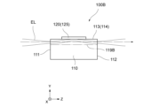
- the optical element 110 may be provided with a slab waveguide arranged so that the processing light EL incident from the incident surface 111 passes through a region in the optical element 110 where the refractive index is changed. Since the optical path of the processing light EL continues at a position close to the electrode due to the slab waveguide, the interaction between the processing light EL and the electric field can be obtained over a long distance. Therefore, the driving voltage for obtaining the desired diffraction efficiency can be lowered, and the processing light EL can be modulated at high speed.
- the slab waveguide 119A may be arranged so that the processing light EL incident from the incident surface 111 passes linearly parallel to the arrangement surface 113.
- the slab waveguide 119B may be configured so that the processing light EL incident on the incident surface 111 passes through after being totally reflected at the positions of the positive and negative electrodes 120, 125 on the placement surface 113.
- a Raman-Nath diffraction type diffraction grating is generated in the spatial light modulation element 100, but this is not limited to this, and it is also possible to generate a Bragg diffraction type diffraction grating.
- the spatial light modulation element applicable to the above-mentioned optical processing apparatuses 1, 51, and 61 is not limited to the spatial light modulation element 100 according to the first embodiment, but may be the spatial light modulation elements according to the second to sixth embodiments.
- the spatial light modulation element according to the second embodiment will be described.
- the spatial light modulation element according to the second embodiment is a line-type electro-optical spatial light modulation element, and has a configuration advantageous for Bragg diffraction. As shown in FIGS.
- the spatial light modulation element 200 includes an optical member 210, a plurality of positive electrodes 220, a plurality of negative electrodes 225, a plurality of positive wires 230, and a plurality of negative wires 235.
- the spatial light modulation element 200 modulates and emits a sheet-shaped processing light EL having a cross-sectional shape shaped into a flattened ellipse.
- the directions indicated by the arrows in FIG. 18 may be referred to as the X direction, Y direction, and Z direction, respectively.
- the X direction, Y direction, and Z direction are mutually perpendicular directions.
- the spatial light modulation element 200 according to the second embodiment is disposed tilted (rotated) around the Y axis by the Bragg angle with respect to the direction in which the processing light EL travels (Z direction).
- the direction tilted by the Bragg angle with respect to the Z direction may be referred to as the Z1 direction
- the direction tilted by the Bragg angle with respect to the X direction may be referred to as the X1 direction.
- the X1 direction, Y direction, and Z1 direction are mutually perpendicular directions.
- the optical member 210 is formed in the same manner as the optical member 110 according to the first embodiment.
- An incident surface 211 is formed at one end (in the -Z1 direction) of the optical member 110.
- a sheet-shaped (elliptical in cross section) processed light EL traveling in the Z direction as incident light is incident on the incident surface 211.
- the Z direction may be referred to as the first axis direction, and the incident surface 111 may intersect with the first axis.
- the Z1 direction may be referred to as the direction along the first axis.
- An exit surface 212 is formed at the end (in the +Z1 direction) of the optical member 210 opposite the incident surface 211. The light that enters the optical member 210 from the incident surface 211 is emitted from the exit surface 212.
- An arrangement surface 213 on which positive and negative electrodes 220, 225 are arranged is formed on a side surface on the +Y direction side of the optical member 210.
- a plurality of pairs of positive and negative electrodes 220, 225 are arranged along the X1 direction on the arrangement surface 213.
- the positive and negative electrodes 220, 225 are formed using a metal material including, for example, gold (Au).
- a buffer layer 214 (see FIG. 21) is formed between the arrangement surface 213 and the plurality of pairs of positive and negative electrodes 220, 225.
- the buffer layer 214 is formed using, for example, silicon dioxide (SiO 2 ).
- the X1 direction may be referred to as the second axis direction, and the Y direction may be referred to as the third axis direction.
- the arrangement surface 213 may also intersect with the third axis.
- the optical member 210 has a periodic polarization reversal structure, similar to the optical member 110 according to the first embodiment.
- the optical member 210 has a first polarization portion 215 extending in the Z1 direction and a second polarization portion 216 adjacent to the first polarization portion 215 extending in the Z1 direction, which are arranged alternately along the X1 direction.
- the optical member 210 may have at least nine first polarization portions 215 and at least eight second polarization portions 216.
- the optical member 210 may have at least fifteen first polarization portions 215 and at least fourteen second polarization portions 216.
- the second polarization portions 216 are polarized in a different direction (specifically, the opposite direction) from the first polarization portions 215.
- the optical element 210 is provided with a periodic polarization inversion structure.
- the second polarization portion 216 which is located adjacent to the first polarization portion 215 on the -X1 direction side, may be referred to as the third polarization portion.
- a positive electrode 220 is provided at a position on the arrangement surface 213 spanning the first polarization portion 215 and the second polarization portion 216 (third polarization portion) located adjacent to the first polarization portion 215 on the -X1 direction side.
- the positive electrode 220 is formed extending in the Z1 direction from one end side to the other end side of the first polarization portion 215 (and the third polarization portion).
- a negative electrode 225 is provided at a position on the arrangement surface 213 spanning the first polarization portion 215 and the second polarization portion 216 located adjacent to the first polarization portion 215 on the +X1 direction side.
- the negative electrode 225 is formed extending in the Z1 direction parallel to the positive electrode 220 from one end side to the other end side of the first polarization portion 215 (and the second polarization portion 216). It can also be said that the positive electrode 220 is provided at a position on the arrangement surface 213 that spans the second polarization portion 216 and the first polarization portion 215 that is adjacent to the second polarization portion 216 on the +X1 direction side (opposite the negative electrode 225).
- the positive electrode 220 that spans the second polarization portion 216 and the first polarization portion 215 that is adjacent to the second polarization portion 216 on the +X1 direction side (opposite the negative electrode 225) may be referred to as a third electrode.
- the multiple positive electrodes 220 are individually electrically connected to multiple positive wires 230.
- the multiple positive wires 230 are electrically connected to the drive circuit 22 described above.
- the multiple positive wires 230 apply the voltage supplied from the drive circuit 22 to the multiple positive electrodes 220 individually. By applying a voltage to the positive electrode 220 via the positive wire 230, a potential difference can be created between adjacent positive and negative electrodes 220, 225.
- the multiple negative electrodes 225 are individually electrically connected to multiple ground wires 235.
- the multiple ground wires 235 are electrically connected to the drive circuit 22.
- the multiple positive wires 230 and the multiple ground wires 235 constitute the wiring EW described above.
- sheet-shaped (elliptical in cross section) processed light EL is incident on the incident surface 211 of the optical element 210 as incident light.
- the sheet-shaped processed light EL that enters the inside of the optical element 210 from the incident surface 211 is totally reflected at the positions of the positive and negative electrodes 220, 225 on the arrangement surface 213, and is emitted from the exit surface 212 as zero-order diffracted light.
- the optical element 210 has a periodic polarization reversal structure.
- the polarization directions in the first polarization portion 215 and the second polarization portion 216 are shown diagrammatically by thick arrows.
- the graph shown in FIG. 21 also shows the change in refractive index in the first polarization portion 215 and the second polarization portion 216.
- a voltage is applied to the positive electrode 220 that spans the first polarization section 215 and the second polarization section 216 (third polarization section) that is adjacent to the first polarization section 215 on the -X1 direction side. Then, in the portion of the arrangement surface 213 where the first polarization section 215 is located, an electric field is generated from the positive electrode 220 toward the first polarization section 215, and the electric field gradually changes direction toward the adjacent negative electrode 225 on the +X1 direction side. As the electric field moves from the positive electrode 220 toward the adjacent negative electrode 225 on the +X1 direction side, the refractive index inside the first polarization section 215 changes due to the electro-optical effect. The refractive index of the region inside the first polarization section 215 near the arrangement surface 213 changes along the X1 direction, for example, so that the refractive index is higher the closer to the positive electrode 220 and lower the closer to the negative electrode 225.
- a voltage is applied to the positive electrode 220 (third electrode) that spans the second polarization portion 216 and the first polarization portion 215 that is located adjacent to the second polarization portion 216 on the +X1 direction side. Then, in the portion of the arrangement surface 213 where the second polarization portion 216 is located, an electric field is generated from the positive electrode 220 toward the negative electrode 225, and the electric field gradually changes direction toward the adjacent negative electrode 225 on the -X1 direction side. In the process in which the electric field flows from the positive electrode 220 toward the adjacent negative electrode 225 on the -X1 direction side, the refractive index within the second polarization portion 216 changes due to the electro-optical effect.
- the second polarization portion 216 is polarized in a different direction (specifically, the opposite direction) from the first polarization portion 215. Therefore, the refractive index of the region inside the second polarizing portion 216 near the placement surface 213 changes along the X1 direction, for example, so that the refractive index is lower the closer to the positive electrode 220 and higher the closer to the negative electrode 225.
- a diffraction grating 217 having a pitch direction along the X1 direction is generated in the region inside the optical member 210 (the first polarizing portion 215 and the second polarizing portion 216) where the refractive index changes.
- the sheet-like processed light EL that enters the inside of the optical element 210 from the incident surface 211 is diffracted by Bragg diffraction in the area where the diffraction grating 217 is generated (i.e., the area where the refractive index is changed).
- the diffracted light DL e.g., +1st order diffracted light
- the diffracted light DL is totally reflected at the positions of the positive and negative electrodes 220, 225 on the arrangement surface 213 and is emitted from the exit surface 212.
- the spatial light modulation element 200 modulates the processed light EL that enters the incident surface 211 of the optical element 210 by the potential difference between the adjacent positive and negative electrodes 220, 225, and emits the diffracted light DL from the exit surface 212.
- the conventional spatial light modulation element 150 described in the first embodiment.
- the distance between the positive and negative electrodes 170, 175 is 20 ⁇ m
- the period ⁇ of the diffraction grating 167 is 40 ⁇ m.
- the spatial light modulation element 200 according to the second embodiment has a periodic polarization inversion structure, and the first polarization portion 215 and the second polarization portion 216 have the same refractive index change due to the potential difference between the positive and negative electrodes 220, 225. Therefore, in the spatial light modulation element 200 according to the second embodiment, a periodic polarization inversion structure with a period of 40 ⁇ m and a duty ratio of 1:1 is used, and the distance between the positive and negative electrodes 220, 225 is kept at 20 ⁇ m. In this case, the period ⁇ of the diffraction grating 217 is 20 ⁇ m.
- the period of the diffraction grating 217 in the spatial light modulation element 200 according to the second embodiment is 1/2 the period of the diffraction grating 167 in the conventional spatial light modulation element 150.
- the periodic polarization inversion structure with a period of 40 ⁇ m and a duty ratio of 1:1 can be easily manufactured because the period is relatively long.
- the wavelength ⁇ of the incident light (processing light) is 1 ⁇ m
- the thickness (interaction length) L of the diffraction grating 217 is 2.24 mm, which is the same as the thickness (interaction length) L of the diffraction grating 117 according to the first embodiment.
- Q ⁇ 16 according to the above-mentioned formula (1), and a Bragg diffraction type diffraction grating can be generated.
- the diffraction efficiency is proportional to the square of the Bessel function of the thickness (interaction length) L of the diffraction grating.
- the thickness (interaction length) L of the diffraction grating 217 can be made larger than 2.24 mm, so that the desired diffraction efficiency can be obtained at a lower voltage than when the conventional spatial light modulation element 150 is used.
- the desired diffraction efficiency can be obtained at a low voltage, the burden on the drive circuit is reduced and the processed light EL can be modulated at high speed.
- the period of the diffraction grating 217 is shortened, the processed light EL can be modulated finely.
- the multiple positive electrodes 220 are individually electrically connected to the drive circuit 22 via multiple positive lines 230.
- the multiple negative electrodes 225 are individually electrically connected to the drive circuit 22 via multiple ground lines 235.
- the drive circuit 22 independently controls the voltage for each control group consisting of at least three pairs of positive and negative electrodes 220, 225, so that a portion of the incident light (processed light EL) can be independently modulated.
- a voltage may be applied to the positive electrodes 220 of the first to third pairs of positive and negative electrodes 220, 225 counting from the bottom of the paper in Fig. 19 to independently modulate the light of the end 1/3 of the sheet-shaped processing light EL in the -X direction, and emit diffracted light DL from the emission surface 212.
- a voltage may be applied to the positive electrodes 220 of the fourth to sixth pairs of positive and negative electrodes 220, 225 counting from the bottom of the paper in Fig. 19 to independently modulate the light of the central 1/3 of the sheet-shaped processing light EL, and emit diffracted light DL from the emission surface 212.
- the light in the 1/3 portion on the end side in the +X direction of the sheet-like processing light EL can be independently modulated, and diffracted light DL can be emitted from the emission surface 212.
- the positive and negative electrodes 220, 225 are arranged in the X1 direction, which is inclined by the Bragg angle with respect to the X direction in which the lenses 24 of the lens array 23 are arranged.
- the lens 24 located at the end of the -X direction may be arranged opposite the portion (exit surface 212) of the optical member 210 where the first to third pairs of positive and negative electrodes 220, 225 are arranged.
- the lens 24 located in the center may be arranged opposite the portion (exit surface 212) of the optical member 210 where the fourth to sixth pairs of positive and negative electrodes 220, 225 are arranged.
- the lens 24 located at the end of the +X direction may be arranged opposite the portion (exit surface 212) of the optical member 210 where the seventh to ninth pairs of positive and negative electrodes 220, 225 are arranged.
- the spatial light modulation element 200 includes an optical member 210 formed using a ferroelectric material having translucency, on which the processing light EL traveling along the Z direction (first axis) is incident as incident light, positive and negative electrodes 220, 225 arranged on the arrangement surface 213 of the optical member 210 along the X1 direction (second axis), and wiring (a positive line 230 and a ground line 235) that applies a voltage to the positive electrode 220 so that a potential difference is created between the positive and negative electrodes 220, 225.
- an optical member 210 formed using a ferroelectric material having translucency, on which the processing light EL traveling along the Z direction (first axis) is incident as incident light
- positive and negative electrodes 220, 225 arranged on the arrangement surface 213 of the optical member 210 along the X1 direction (second axis)
- wiring a positive line 230 and a ground line 235
- the spatial light modulation element 200 includes the optical member 210, the positive and negative electrodes 220, 225, and when a potential difference is generated between the positive and negative electrodes 220, 225, the refractive index in the optical member 210 changes along the X direction.
- the processed light EL is modulated by the potential difference between the positive and negative electrodes 220, 225, so that the processed light EL (incident light) can be modulated at high speed.
- the positive and negative electrodes 220, 225 are provided only on one side (arrangement surface 213) of the optical member 210, the optical member 210 can be made thick, and even if high-power laser light is used as the processed light EL, the increase in the density of the optical power within the optical member 210 can be suppressed.
- the positive and negative electrodes 220, 225 are provided only on one side of the optical member 210, there is no need to thin the optical member 210, lay electrodes on both sides of the optical member 210, or join a reinforcing member associated with the thinning of the optical member 210, making it easier to manufacture the spatial light modulation element.
- the positive and negative electrodes 220, 225 may be arranged adjacent to each other along the X1 direction.
- the arrangement surface 213 of the optical member 210 may intersect with the Y-axis (third axis).
- the optical member 210 also has a first polarized portion 215 extending along the Z1 direction, and a second polarized portion 216 extending along the Z1 direction and polarized in a different direction from the first polarized portion 215, and located adjacent to the first polarized portion 215 on the X1 direction side.
- the refractive index differs between the position in the optical member 210 where the positive electrode 220 is provided and the position in the optical member 210 where the negative electrode 225 is provided.
- the change in the refractive index in the optical member 210 generates a diffraction grating 217 having a pitch direction along the X direction in the optical member 210.
- the driving voltage for obtaining the desired diffraction efficiency can be reduced, and the processed light EL can be modulated at high speed.
- a positive electrode 220 is provided at a position on the arrangement surface 213 that spans the first polarization section 215 and the second polarization section 216 (third polarization section) located adjacent to the first polarization section 215 on the -X1 direction side.
- a negative electrode 225 is provided at a position on the arrangement surface 213 that spans the first polarization section 215 and the second polarization section 216 located adjacent to the first polarization section 215 on the +X1 direction side.
- An electric field is generated in the first polarization section 215 from the positive electrode 220 toward the negative electrode 225.
- a positive electrode 220 (third electrode section) is provided at a position on the arrangement surface 213 on the opposite side of the negative electrode 225 of the second polarization section 216.
- An electric field is generated in the second polarization section 116 from the positive electrode 220 toward the negative electrode 225.
- This makes it possible to generate a diffraction grating 217 with a short period (grating pitch). Therefore, since the thickness (interaction length) of the diffraction grating can be increased while satisfying the conditions of the Q parameter for obtaining a Bragg diffraction type diffraction grating, the driving voltage for obtaining the desired diffraction efficiency can be reduced, and the processing light EL can be modulated at high speed. In addition, since the period of the diffraction grating 217 is shortened, the processing light EL can be modulated finely.
- the processed light EL incident on the optical element 210 passes through a region in the optical element 210 where the refractive index changes along a direction intersecting the X1 direction.
- the processed light EL incident on the incident surface 211 of the optical element 210 is totally reflected at the positions of the positive and negative electrodes 220, 225 on the arrangement surface 213 and emitted from the emission surface 212. This makes it easier to obtain an interaction between the processed light EL and the electric field, so the driving voltage required to obtain the desired diffraction efficiency can be lowered, and it becomes possible to modulate the processed light EL at high speed.
- the optical element 210 may include a slab waveguide arranged so that the processing light EL incident from the incident surface 211 passes through a region in the optical element 210 where the refractive index is changed.
- the slab waveguide allows the optical path of the processing light EL to continue close to the electrode, so that interaction between the processing light EL and the electric field can be obtained over a long distance. This allows the drive voltage required to obtain the desired diffraction efficiency to be lowered, making it possible to modulate the processing light EL at high speed.
- a Bragg diffraction type diffraction grating is generated in the spatial light modulation element 200, but this is not limited to this, and it is also possible to generate a Raman-Nath diffraction type diffraction grating.
- the spatial light modulation element according to the third embodiment is a line-type electro-optical spatial light modulation element, which generates a Bragg diffraction grating.
- the spatial light modulation element 300 according to the third embodiment includes an optical member 310, a plurality of positive electrodes 320A, 320B, and 320C, a plurality of negative electrodes 325A, 325B, and 325C, a plurality of positive lines (not shown), and a plurality of negative lines (not shown).
- the spatial light modulation element 300 modulates and emits a sheet-shaped processed light EL whose cross-sectional shape is shaped into a flattened ellipse.
- the directions indicated by the arrows in Figure 22 may be referred to as the X direction, Y direction, and Z direction, respectively.
- the X direction, Y direction, and Z direction are mutually perpendicular directions.
- the spatial light modulation element 300 according to the third embodiment is disposed tilted (rotated) around the Y axis by the Bragg angle with respect to the direction in which the processing light EL travels (Z direction).
- the direction tilted by the Bragg angle with respect to the Z direction may be referred to as the Z1 direction
- the direction tilted by the Bragg angle with respect to the X direction may be referred to as the X1 direction.
- the X1 direction, Y direction, and Z1 direction are mutually perpendicular directions.
- the optical member 310 is formed in the same manner as the optical member 110 according to the first embodiment.
- An incident surface 311 is formed at one end (in the -Z1 direction) of the optical member 310.
- a sheet-shaped (elliptical in cross section) processed light EL traveling in the Z direction as incident light is incident on the incident surface 311.
- the Z direction may be referred to as the first axis direction, and the incident surface 311 may intersect with the first axis.
- the Z1 direction may be referred to as the direction along the first axis.
- An exit surface 312 is formed at the end (in the +Z1 direction) of the optical member 310 opposite the incident surface 311. The light that enters the optical member 310 from the incident surface 311 is emitted from the exit surface 312.
- the arrangement surface 313 on which the multiple positive electrodes 320A, 320B, 320C and the multiple negative electrodes 325A, 325B, 325C are arranged is formed on the side surface on the +Y direction side of the optical member 310.
- the multiple positive electrodes 320A, 320B, 320C and the multiple negative electrodes 325A, 325B, 325C are formed using a metal material containing, for example, gold (Au).
- a buffer layer 314 is formed between the arrangement surface 313 and the multiple positive electrodes 320A, 320B, 320C and the multiple negative electrodes 325A, 325B, 325C.
- the optical member 310 has a periodic polarization inversion structure, similar to the optical member 110 according to the first embodiment.
- the optical member 310 has first polarization sections 315 extending in the Z1 direction and second polarization sections 316 adjacent to the first polarization sections 315 and extending in the Z1 direction, arranged alternately along the X1 direction.
- the second polarization sections 316 are polarized in a different direction (specifically, the opposite direction) from the first polarization sections 315.
- the X1 direction may be referred to as the second axis direction
- the Y direction may be referred to as the third axis direction.
- the placement surface 313 may also intersect with the third axis.
- a pair of positive and negative electrodes 320A, 325A are provided in the portion where the first polarization portion 315 is located.
- the positive and negative electrodes 320A, 325A of the first region 301A are formed extending parallel to the Z1 direction from one end side to the other end side of the first region 301A in the portion where the first polarization portion 315 is located on the placement surface 313.
- the negative electrode 325A of the first region 301A is arranged adjacent to the positive electrode 320A of the first region 301A on the +X1 direction side.
- the positive and negative electrodes 320A, 325A of the first region 301A may be referred to as the first and second electrodes of the first region 301A in the portion where the first polarization portion 315 is located on the placement surface 313.
- a pair of positive and negative electrodes 320A, 325A are provided in the portion where the second polarization portion 316 is located.
- the positive and negative electrodes 320A, 325A of the first region 301A are formed in the portion where the second polarization portion 316 is located on the arrangement surface 313, extending parallel to the Z1 direction from one end side to the other end side of the first region 301A.
- the negative electrode 325A of the first region 301A is arranged adjacent to the positive electrode 320A of the first region 301A on the +X1 direction side.
- the positive and negative electrodes 320A, 325A of the first region 301A may be referred to as the third and fourth electrodes of the first region 301A in the portion where the second polarization portion 316 is located on the arrangement surface 313.
- a pair of positive and negative electrodes 320B, 325B is provided in each portion where the first polarization portion 315 is located.
- the positive and negative electrodes 320B, 325B of the second region 301B are formed extending parallel to the Z1 direction from one end side to the other end side of the second region 301B in the portion where the first polarization portion 315 is located on the arrangement surface 313.
- the negative electrode 325B of the second region 301B is arranged adjacent to the +X1 direction side of the positive electrode 320B of the second region 301B.
- the positive and negative electrodes 320B, 325B of the second region 301B may be referred to as the first and second electrodes of the second region 301B in the portion of the placement surface 313 where the first polarized portion 315 is located.
- a pair of positive and negative electrodes 320B, 325B are provided in the portion where the second polarization portion 316 is located.
- the positive and negative electrodes 320B, 325B of the second region 301B are formed in the portion where the second polarization portion 316 is located on the placement surface 313, extending parallel to the Z1 direction from one end side to the other end side of the second region 301B.
- the negative electrode 325B of the second region 301B is arranged adjacent to the positive electrode 320B of the second region 301B on the +X1 direction side.
- the positive and negative electrodes 320B, 325B of the second region 301B may be referred to as the third and fourth electrodes of the second region 301B in the portion where the second polarization portion 316 is located on the placement surface 313.
- a pair of positive and negative electrodes 320C, 325C is provided in each portion where the first polarization portion 315 is located.
- the positive and negative electrodes 320C, 325C of the third region 301C are formed extending parallel to the Z1 direction from one end side to the other end side of the third region 301C in the portion where the first polarization portion 315 is located on the placement surface 313.
- the negative electrode 325C of the third region 301C is arranged adjacent to the +X1 direction side of the positive electrode 320C of the third region 301C.
- the positive and negative electrodes 320C, 325C of the third region 301C may be referred to as the first and second electrodes of the third region 301C in the portion of the placement surface 313 where the first polarized portion 315 is located.
- a pair of positive and negative electrodes 320C, 325C are provided in the portion where the second polarization portion 316 is located.
- the positive and negative electrodes 320C, 325C of the third region 301C are formed in the portion where the second polarization portion 316 is located on the arrangement surface 313, extending parallel to the Z1 direction from one end side to the other end side of the third region 301C.
- the negative electrode 325C of the third region 301C is arranged adjacent to the positive electrode 320C of the third region 301C on the +X1 direction side.
- the positive and negative electrodes 320C, 325C of the third region 301C may be referred to as the third and fourth electrodes of the third region 301C in the portion where the second polarization portion 316 is located on the arrangement surface 313.
- the positive and negative electrodes 320A, 325A of the first region 301A, the positive and negative electrodes 320B, 325B of the second region 301B, and the positive and negative electrodes 320C, 325C of the third region 301C are provided separately from each other along the Z1 direction. Also, as shown by hatching in FIG.
- the positive and negative electrodes 320A, 325A of the first region 301A in the first polarization portion 315, the positive and negative electrodes 320B, 325B of the second region 301B in the second polarization portion 316 adjacent to the +X1 direction side of the first polarization portion 315, and the positive and negative electrodes 320C, 325C of the third region 301C in the other first polarization portion 315 adjacent to the +X1 direction side of the second polarization portion 316 are arranged side by side along the traveling direction of the diffracted light DL due to Bragg diffraction.
- the positive and negative electrodes 320A, 325A of the first region 301A in the second polarization section 316, the positive and negative electrodes 320B, 325B of the second region 301B in the first polarization section 315 adjacent to the +X1 direction side of the second polarization section 316, and the positive and negative electrodes 320C, 325C of the third region 301C in the other second polarization section 316 adjacent to the +X1 direction side of the first polarization section 315 are arranged side by side along the traveling direction of the diffracted light DL due to Bragg diffraction.
- the multiple positive electrodes 320A, 320B, 320C are individually electrically connected to multiple positive wires (not shown).
- the multiple positive wires are electrically connected to the drive circuit 22 described above.
- the multiple positive wires apply the voltage supplied from the drive circuit 22 to the multiple positive electrodes 320A, 320B, 320C individually. By applying a voltage to the positive electrodes via the positive wires, a potential difference can be created between adjacent positive and negative electrodes.
- the multiple negative electrodes 325A, 325B, 325C are individually electrically connected to multiple ground wires (not shown).
- the multiple ground wires are electrically connected to the drive circuit 22.
- the multiple positive wires and multiple ground wires constitute the wiring EW described above.
- sheet-shaped (elliptical in cross section) processed light EL is incident on the incident surface 311 of the optical element 310 as incident light.
- the sheet-shaped processed light EL that enters the inside of the optical element 310 from the incident surface 311 is totally reflected at the arrangement surface 313 inside the optical element 310 and is emitted from the exit surface 312 as zero-order diffracted light.
- a first diffraction grating (not shown) of the Bragg diffraction type having a pitch direction along the X1 direction is generated in the region where the refractive index changes inside the optical member 310 (first polarization section 315 and second polarization section 316) located in the first region 301A.
- a second diffraction grating (not shown) of the Bragg diffraction type having a pitch direction along the X1 direction is generated in the region where the refractive index changes inside the optical member 310 (first polarization section 315 and second polarization section 316) located in the second region 301B.
- a third diffraction grating (not shown) of the Bragg diffraction type having a pitch direction along the X1 direction is generated in the region where the refractive index changes inside the optical member 310 (first polarization section 315 and second polarization section 316) located in the third region 301C.
- the sheet-like processed light EL that enters the inside of the optical element 310 from the incident surface 311 is diffracted by Bragg diffraction in the area where the first to third diffraction gratings are generated (i.e., the area where the refractive index changes).
- the diffracted light DL e.g., +1st order diffracted light
- the spatial light modulation element 300 modulates the processed light EL that enters the incident surface 311 of the optical element 310 by the potential difference between the adjacent positive and negative electrodes, and emits the diffracted light DL from the exit surface 312.
- the positive and negative electrodes 320A, 325A of the first region 301A in the first polarization portion 315, the positive and negative electrodes 320B, 325B of the second region 301B in the second polarization portion 316 adjacent to the +X1 direction side of the first polarization portion 315, and the positive and negative electrodes 320C, 325C of the third region 301C in the other first polarization portion 315 adjacent to the +X1 direction side of the second polarization portion 316 are arranged in a row along the traveling direction of the diffracted light DL due to Bragg diffraction.
- the positive and negative electrodes 320A, 325A of the first region 301A in the second polarization section 316, the positive and negative electrodes 320B, 325B of the second region 301B in the first polarization section 315 adjacent to the +X1 direction side of the second polarization section 316, and the positive and negative electrodes 320C, 325C of the third region 301C in the other second polarization section 316 adjacent to the +X1 direction side of the first polarization section 315 are arranged side by side along the traveling direction of the diffracted light DL due to Bragg diffraction. This makes it possible to clearly define the boundary of the applied voltage when viewed from the traveling direction of the diffracted light DL due to Bragg diffraction.
- the multiple positive electrodes 320A, 320B, 320C are individually electrically connected to the drive circuit 22 via multiple positive lines (not shown).
- the multiple negative electrodes 325A, 325B, 325C are individually electrically connected to the drive circuit 22 via multiple ground lines (not shown).
- the driving circuit 22 independently controls the voltage for each control group consisting of at least six pairs of combinations of positive and negative electrodes 320A, 325A in the first region 301A, positive and negative electrodes 320B, 325B in the second region 301B, and positive and negative electrodes 320C, 325C in the third region 301C, which are aligned along the direction of travel of the diffracted light DL due to Bragg diffraction, thereby independently modulating a portion of the incident light (processed light EL).
- a plurality of positive and negative electrodes 320A, 325A that generate a first diffraction grating are provided along the X1 direction (second axis) in the first region 301A on the arrangement surface 313 of the optical member 310.
- a plurality of positive and negative electrodes 320B, 325B that generate a second diffraction grating are provided along the X1 direction in the second region 301B on the arrangement surface 313 of the optical member 310.
- a plurality of positive and negative electrodes 320C, 325C that generate a third diffraction grating are provided along the X1 direction in the third region 301C on the arrangement surface 313 of the optical member 310.
- the positive and negative electrodes 320A, 325A of the first region 301A, the positive and negative electrodes 320B, 325B of the second region 301B, and the positive and negative electrodes 320C, 325C of the third region 301C are arranged side by side along the direction of propagation of the diffracted light DL due to Bragg diffraction. In such an arrangement (for example, the arrangement shown by hatching in FIG.
- the first diffraction grating generated by the positive and negative electrodes 320A, 325A of the first region 301A, the second diffraction grating generated by the positive and negative electrodes 320B, 325B of the second region 301B, and the third diffraction grating generated by the positive and negative electrodes 320C, 325C of the third region 301C have different phases of refractive index change in the X1 direction.
- phase of the refractive index change of the second diffraction grating and the third diffraction grating is equal to the phase of the refractive index change of the first diffraction grating in a direction perpendicular to the traveling direction of the diffracted light DL due to Bragg diffraction. This makes it possible to clearly define the boundary of the applied voltage when viewed from the traveling direction of the diffracted light DL due to Bragg diffraction.
- the positive and negative electrodes 320A, 325A in the first region 301A, the positive and negative electrodes 320B, 325B in the second region 301B, and the positive and negative electrodes 320C, 325C in the third region 301C are provided separately from each other along the Z1 direction, but this is not limited to this.
- the positive and negative electrodes 370A, 375A in the first region 301A, the positive and negative electrodes 370B, 375B in the second region 301B, and the positive and negative electrodes 370C, 375C in the third region 301C that are aligned along the traveling direction of the diffracted light DL due to Bragg diffraction may be formed by connecting the electrodes that are located at the same position in the X1 direction.
- the second pair of positive and negative electrodes counting in the X1 direction may be formed by connecting the positive and negative electrodes 370A, 375A in the first region 301A to the positive and negative electrodes 370B, 375B in the second region 301B.
- the third to sixth pairs of positive and negative electrodes counting in the X1 direction may be formed by connecting the positive and negative electrodes 370A, 375A in the first region 301A to the positive and negative electrodes 370B, 375B in the second region 301B to the positive and negative electrodes 370C, 375C in the third region 301C.
- the positive and negative electrodes 370B, 375B of the second region 301B may be connected to the positive and negative electrodes 370C, 375C of the third region 301C.
- the optical element 310 may include a slab waveguide arranged so that the processing light EL incident from the incident surface 311 passes through a region in the optical element 310 where the refractive index is changed.
- the slab waveguide allows the optical path of the processing light EL to continue close to the electrode, so that interaction between the processing light EL and the electric field can be obtained over a long distance. Therefore, the driving voltage required to obtain the desired diffraction efficiency can be reduced, making it possible to modulate the processing light EL at high speed.
- the spatial light modulation element according to the fourth embodiment is a line-type electro-optical spatial light modulation element that generates a Bragg diffraction grating.
- the spatial light modulation element 400 according to the fourth embodiment includes an optical member 410, a plurality of positive electrodes 420A to 420E, a plurality of negative electrodes 425A to 425E, a plurality of positive lines (not shown), and a plurality of negative lines (not shown).
- the spatial light modulation element 400 modulates and emits a sheet-shaped processed light EL whose cross-sectional shape is shaped into a flattened ellipse.
- the directions indicated by the arrows in FIG. 25 may be referred to as the X direction, Y direction, and Z direction, respectively.
- the X direction, Y direction, and Z direction are mutually perpendicular directions.
- the spatial light modulation element 400 according to the fourth embodiment is disposed tilted (rotated) around the Y axis by the Bragg angle with respect to the direction in which the processing light EL travels (Z direction).
- the direction tilted by the Bragg angle with respect to the Z direction may be referred to as the Z1 direction
- the direction tilted by the Bragg angle with respect to the X direction may be referred to as the X1 direction.
- the X1 direction, Y direction, and Z1 direction are mutually perpendicular directions.
- the optical member 410 is formed in the same manner as the optical member 210 according to the second embodiment.
- An incident surface 411 is formed at one end (in the -Z1 direction) of the optical member 410.
- a sheet-shaped (elliptical in cross section) processed light EL traveling in the Z direction as incident light is incident on the incident surface 411.
- the Z direction may be referred to as the first axis direction, and the incident surface 411 may intersect with the first axis.
- the Z1 direction may be referred to as the direction along the first axis.
- An exit surface 412 is formed at the end (in the +Z1 direction) of the optical member 410 opposite the incident surface 411. The light that enters the optical member 410 from the incident surface 411 is emitted from the exit surface 412.
- An arrangement surface 413 on which multiple positive electrodes 420A-420E and multiple negative electrodes 425A-425E are arranged is formed on the side surface on the +Y direction side of the optical member 410.
- the multiple positive electrodes 420A-420E and multiple negative electrodes 425A-425E are formed using a metal material containing, for example, gold (Au).
- a buffer layer 414 is formed between the arrangement surface 413 and the multiple positive electrodes 420A-420E and multiple negative electrodes 425A-425E.
- the optical member 410 has a periodic polarization inversion structure, similar to the optical member 210 according to the second embodiment.
- the optical member 410 has a first polarization portion 415 extending in the Z1 direction and a second polarization portion 416 adjacent to the first polarization portion 415 and extending in the Z1 direction, which are arranged alternately along the X1 direction.
- the second polarization portion 416 is polarized in a different direction (specifically, the opposite direction) from the first polarization portion 415.
- the X1 direction may be referred to as the second axis direction
- the Y direction may be referred to as the third axis direction.
- the arrangement surface 413 may also intersect with the third axis.
- a positive electrode 420A is provided at a position straddling the first polarization portion 415 and the second polarization portion 416 (third polarization portion) located adjacent to the first polarization portion 415 on the -X1 direction side.
- the positive electrode 420A in the first region 401A is formed extending in the Z1 direction from one end side to the other end side of the first region 401A at a position straddling the first polarization portion 415 and the second polarization portion 416 (third polarization portion).
- a negative electrode 425A is provided at a position straddling the first polarization portion 415 and the second polarization portion 416 located adjacent to the first polarization portion 415 on the +X1 direction side.
- the negative electrode 425A of the first region 401A is formed to extend in the Z1 direction parallel to the positive electrode 420A from one end side to the other end side of the first region 401A at a position spanning the first polarization portion 415 and the second polarization portion 416.
- the positive electrode 420A is provided at a position spanning the second polarization portion 416 and the first polarization portion 415 located adjacent to the second polarization portion 416 on the +X1 direction side (opposite side to the negative electrode 425A) in the first region 401A.
- the positive electrode 420A spanning the second polarization portion 416 and the first polarization portion 415 located adjacent to the second polarization portion 416 on the +X1 direction side (opposite side to the negative electrode 425) may be referred to as a third electrode.
- the positive and negative electrodes 420B, 425B of the second region 401B are provided similarly to the positive and negative electrodes 420A, 425A of the first region 401A.
- the positive and negative electrodes 420C, 425C of the third region 401C are provided similarly to the positive and negative electrodes 420A, 425A of the first region 401A.
- the positive and negative electrodes 420D, 425D of the fourth region 401D are provided similarly to the positive and negative electrodes 420A, 425A of the first region 401A.
- a fifth region 401E adjacent to the +Z1 direction side of the fourth region 401D on the placement surface 413 (the end side of the placement surface 413 in the +Z1 direction) positive and negative electrodes 420E, 425E of the fifth region 401E are provided, similar to the positive and negative electrodes 420A, 425A of the first region 401A.
- the positive and negative electrodes 420A, 425A in the first region 401A, the positive and negative electrodes 420B, 425B in the second region 401B, the positive and negative electrodes 420C, 425C in the third region 401C, the positive and negative electrodes 420D, 425D in the fourth region 401D, and the positive and negative electrodes 420E, 425E in the fifth region 401E are arranged separated from each other along the Z1 direction. As shown by hatching in FIG.
- the positive and negative electrodes 420A, 425A of the first region 401A in the first polarization portion 415, the positive and negative electrodes 420B, 425B of the second region 401B in the first polarization portion 415 arranged on the +X1 direction side of the first polarization portion 415 (via the second polarization portion 416), and the positive and negative electrodes 420C, 425D of the third region 401C in the first polarization portion 415 arranged on the +X1 direction side of the first polarization portion 415 (via the second polarization portion 416) are The electrodes 420C, 425C, the positive and negative electrodes 420D, 425D of the fourth region 401D in the first polarization section 415 aligned on the +X1 direction side of the first polarization section 415 (via the second polarization section 416), and the positive and negative electrodes 420E, 425E of the fifth region 501E in the first polarization section 415 aligned on the +X
- the multiple positive electrodes 420A-420E are individually electrically connected to multiple positive wires (not shown).
- the multiple positive wires are electrically connected to the drive circuit 22 described above.
- the multiple positive wires apply the voltage supplied from the drive circuit 22 to the multiple positive electrodes 420A-420E individually. By applying a voltage to the positive electrodes via the positive wires, a potential difference can be created between adjacent positive and negative electrodes.
- the multiple negative electrodes 425A-425E are individually electrically connected to multiple ground wires (not shown).
- the multiple ground wires are electrically connected to the drive circuit 22.
- the multiple positive wires and multiple ground wires constitute the wiring EW described above.
- sheet-shaped (elliptical in cross section) processed light EL is incident on the incident surface 411 of the optical member 410 as incident light.
- the sheet-shaped processed light EL that enters the inside of the optical member 410 from the incident surface 411 is totally reflected at the arrangement surface 413 inside the optical member 410 and is emitted from the exit surface 412 as zero-order diffracted light.
- a first diffraction grating (not shown) of the Bragg diffraction type having a pitch direction along the X1 direction is generated in the region where the refractive index changes inside the optical member 410 (first polarization section 415 and second polarization section 416) located in the first region 401A.
- a second diffraction grating (not shown) of the Bragg diffraction type having a pitch direction along the X1 direction is generated in the region where the refractive index changes inside the optical member 410 (the first polarization section 415 and the second polarization section 416) located in the second region 401B.
- a third diffraction grating (not shown) of the Bragg diffraction type having a pitch direction along the X1 direction is generated in the region where the refractive index changes inside the optical member 410 (first polarization section 415 and second polarization section 416) located in the third region 401C.
- a fourth diffraction grating (not shown) of the Bragg diffraction type having a pitch direction along the X1 direction is generated in the region where the refractive index changes inside the optical member 410 (first polarization section 415 and second polarization section 416) located in the fourth region 401D.
- a fifth diffraction grating (not shown) of the Bragg diffraction type having a pitch direction along the X1 direction is generated in the region where the refractive index changes inside the optical member 410 (first polarization section 415 and second polarization section 416) located in the fifth region 401E.
- the sheet-like processed light EL that enters the inside of the optical element 410 from the incident surface 411 is diffracted by Bragg diffraction in the areas where the first to fifth diffraction gratings are generated (i.e., the areas where the refractive index changes).
- the diffracted light DL e.g., +1st order diffracted light
- the spatial light modulation element 400 modulates the processed light EL that enters the incident surface 411 of the optical element 410 by the potential difference between the adjacent positive and negative electrodes, and emits the diffracted light DL from the emission surface 412.
- the electrodes are rotated in the direction in which light is diffracted, with positive and negative electrodes 420A, 425A of the first region 401A in the first polarization section 415, positive and negative electrodes 420B, 425B of the second region 401B in the first polarization section 415 aligned on the +X1 direction side of the first polarization section 415 (via the second polarization section 416), and positive and negative electrodes 420C, 425D of the third region 401C in the first polarization section 415 aligned on the +X1 direction side of the first polarization section 415 (via the second polarization section 416).
- the positive and negative electrodes 420D, 425D of the fourth region 401D in the first polarization section 415 aligned on the +X1 direction side of the first polarization section 415 (via the second polarization section 416), and the positive and negative electrodes 420E, 425E of the fifth region 501E in the first polarization section 415 aligned on the +X1 direction side of the first polarization section 415 (via the second polarization section 416) are arranged in line along the traveling direction of the diffracted light DL due to Bragg diffraction. This makes it possible to clearly define the boundary of the applied voltage when viewed from the traveling direction of the diffracted light DL due to Bragg diffraction.
- the multiple positive electrodes 420A-420E are individually electrically connected to the drive circuit 22 via multiple positive lines (not shown).
- the multiple negative electrodes 425A-425E are individually electrically connected to the drive circuit 22 via multiple ground lines (not shown).
- the driving circuit 22 independently controls the voltage for each control group consisting of at least three pairs of combinations of positive and negative electrodes 420A, 425A in the first region 401A, a pair of positive and negative electrodes 420B, 425B in the second region 401B, a pair of positive and negative electrodes 420C, 425C in the third region 401C, a pair of positive and negative electrodes 420D, 425D in the fourth region 401D, and a pair of positive and negative electrodes 420E, 425E in the fifth region 401E, which are aligned along the direction of travel of the diffracted light DL due to Bragg diffraction, thereby independently modulating a portion of the incident light (processed light EL).
- a plurality of positive and negative electrodes 420A, 425A that generate a first diffraction grating are provided along the X1 direction (second axis) in the first region 401A on the arrangement surface 413 of the optical member 410.
- a plurality of positive and negative electrodes 420B, 425B that generate a second diffraction grating are provided along the X1 direction in the second region 401B on the arrangement surface 413 of the optical member 410.
- a plurality of positive and negative electrodes 420C, 425C that generate a third diffraction grating are provided along the X1 direction in the third region 401C on the arrangement surface 413 of the optical member 410.
- a plurality of positive and negative electrodes 420D, 425D that generate a fourth diffraction grating are provided along the X1 direction in the fourth region 401D on the arrangement surface 413 of the optical member 410.
- a plurality of positive and negative electrodes 420E, 425E that generate a fifth diffraction grating are provided along the X1 direction.
- the positive and negative electrodes 420A, 425A in the first region 401A, the positive and negative electrodes 420B, 425B in the second region 401B, the positive and negative electrodes 420C, 425C in the third region 401C, the positive and negative electrodes 420D, 425D in the fourth region 401D, and the positive and negative electrodes 420E, 425E in the fifth region 401E are arranged in a line along the direction of propagation of the diffracted light DL due to Bragg diffraction. In such an arrangement (for example, the arrangement shown by hatching in FIG.
- the phases of the refractive index change of the second to fifth diffraction gratings are equal to the phase of the refractive index change of the first diffraction grating in a direction perpendicular to the traveling direction of the diffracted light DL due to Bragg diffraction. This makes it possible to clearly identify the boundary of applied voltage when viewed from the direction in which diffracted light DL due to Bragg diffraction travels.
- the positive and negative electrodes 420A, 425A in the first region 401A, the positive and negative electrodes 420B, 425B in the second region 401B, the positive and negative electrodes 420C, 425C in the third region 401C, the positive and negative electrodes 420D, 425D in the fourth region 401D, and the positive and negative electrodes 420E, 425E in the fifth region 401E are arranged separated from each other along the Z1 direction, but this is not limited to this.
- the positive and negative electrodes 470A, 475A in the first region 401A, the positive and negative electrodes 470B, 475B in the second region 401B, the positive and negative electrodes 470C, 475C in the third region 401C, the positive and negative electrodes 470D, 475D in the fourth region 401D, and the positive and negative electrodes 470E, 475E in the fifth region 401E, which are aligned along the direction of propagation of the diffracted light DL due to Bragg diffraction, may be formed by connecting the electrodes located at the same position in the X1 direction.
- the second pair of positive and negative electrodes counting in the X1 direction may be formed by connecting the positive and negative electrodes 470A, 475A in the first region 401A to the positive and negative electrodes 470B, 475B in the second region 401B.
- the third pair of positive and negative electrodes counting in the X1 direction may be formed by connecting the positive and negative electrodes 470A, 475A in the first region 401A to the positive and negative electrodes 470B, 475B in the second region 401B to the positive and negative electrodes 470C, 475C in the third region 401C.
- the positive and negative electrodes 470B, 475B in the second region 401B, the positive and negative electrodes 470C, 475C in the third region 401C, and the positive and negative electrodes 470D, 475D in the fourth region 401D may be connected to each other.
- the positive and negative electrodes 470C, 475C in the third region 401C, the positive and negative electrodes 470D, 475D in the fourth region 401D, and the positive and negative electrodes 470E, 475E in the fifth region 401E may be connected to each other.
- the positive and negative electrodes 470D, 475D of the fourth region 401D may be connected to the positive and negative electrodes 470E, 475E of the fifth region 401E.
- the optical member 410 may include a slab waveguide arranged so that the processing light EL incident from the incident surface 411 passes through a region in the optical member 410 where the refractive index is changed.
- the slab waveguide allows the optical path of the processing light EL to continue close to the electrode, so that interaction between the processing light EL and the electric field can be obtained over a long distance. Therefore, the driving voltage required to obtain the desired diffraction efficiency can be reduced, making it possible to modulate the processing light EL at high speed.
- the spatial light modulation element according to the fifth embodiment has a configuration in which the main parts are common to the spatial light modulation element 300 according to the third embodiment, except that the spatial light modulation element according to the fifth embodiment further includes a positive side connection and a negative side connection. Therefore, the same components as those in the third embodiment are given the same reference numerals as those in the third embodiment, and detailed descriptions thereof will be omitted. As shown in FIG.
- the spatial light modulation element 500 includes an optical member 310, a plurality of positive electrodes 320A, 320B, and 320C, a plurality of negative electrodes 325A, 325B, and 325C, a plurality of positive wires (not shown), a plurality of negative wires (not shown), first and second positive side connections 540A and 540B, and first and second negative side connections 545A and 545B.
- the spatial light modulation element 500 modulates and emits a sheet-shaped processed light EL whose cross-sectional shape is shaped into a flattened ellipse.
- the first positive side connection 540A electrically connects the positive electrode 320A of the first region 301A and the positive electrode 320B of the second region 301B, which are aligned along the direction of travel of the diffracted light DL due to Bragg diffraction.
- the second positive side connection 540B electrically connects the positive electrode 320B of the second region 301B and the positive electrode 320C of the third region 301C, which are aligned along the direction of travel of the diffracted light DL due to Bragg diffraction.
- the positive electrode 320A of the first region 301A, the positive electrode 320B of the second region 301B, and the positive electrode 320C of the third region 301C which are aligned along the direction of travel of the diffracted light DL due to Bragg diffraction, are electrically connected by the first and second positive side connections 540A and 540B.
- the first negative side connection 545A electrically connects the negative electrode 325A of the first region 301A and the negative electrode 325B of the second region 301B, which are aligned along the direction of the diffracted light DL due to Bragg diffraction.
- the second negative side connection 545B electrically connects the negative electrode 325B of the second region 301B and the negative electrode 325C of the third region 301C, which are aligned along the direction of the diffracted light DL due to Bragg diffraction.
- the negative electrode 325A of the first region 301A, the negative electrode 325B of the second region 301B, and the negative electrode 325C of the third region 301C which are aligned along the direction of the diffracted light DL due to Bragg diffraction, are electrically connected by the first and second negative side connections 545A and 545B.
- the positive electrodes 320A in the first region 301A, the positive electrodes 320B in the second region 301B, and the positive electrodes 320C in the third region 301C are arranged in a line along the direction of travel of the diffracted light DL due to Bragg diffraction, and are electrically connected to a number of positive wires (not shown).
- the positive wires are electrically connected to the aforementioned driving circuit 22.
- the positive wires individually apply a voltage supplied from the driving circuit 22 to the multiple sets of positive electrodes 320A, 320B, 320C arranged in a line along the direction of travel of the diffracted light DL due to Bragg diffraction.
- a set of negative electrodes 325A in the first region 301A, negative electrodes 325B in the second region 301B, and negative electrodes 325C in the third region 301C, which are arranged in a line along the direction of propagation of the diffracted light DL due to Bragg diffraction, are electrically connected to a plurality of ground lines (not shown).
- the plurality of ground lines are electrically connected to the drive circuit 22.
- the plurality of positive lines and the plurality of ground lines constitute the wiring EW described above.
- sheet-shaped (elliptical in cross section) processed light EL is incident on the incident surface 311 of the optical element 310 as incident light.
- the sheet-shaped processed light EL that enters the inside of the optical element 310 from the incident surface 311 is totally reflected at the arrangement surface 313 inside the optical element 310 and is emitted from the exit surface 312 as zero-order diffracted light.
- a voltage (a voltage lower than the aforementioned polarization inversion voltage) is applied to multiple sets of positive electrodes 320A, 320B, 320C arranged along the direction of propagation of diffracted light DL due to Bragg diffraction via multiple positive lines (not shown)
- a first diffraction grating (not shown) of a Bragg diffraction type having a pitch direction along the X1 direction is generated in the region where the refractive index changes inside the optical element 310 (first polarization portion 315 and second polarization portion 316) located in the first region 301A, as in the third embodiment.
- a second diffraction grating (not shown) of a Bragg diffraction type having a pitch direction along the X1 direction is generated in the region where the refractive index changes inside the optical element 310 (first polarization portion 315 and second polarization portion 316) located in the second region 301B.
- a third Bragg diffraction grating (not shown) having a pitch direction along the X1 direction is generated in the region where the refractive index changes inside the optical member 310 (first polarized portion 315 and second polarized portion 316) located in the third region 301C.
- the sheet-like processed light EL that enters the inside of the optical element 310 from the incident surface 311 is diffracted by Bragg diffraction in the area where the first to third diffraction gratings are generated (i.e., the area where the refractive index changes).
- the diffracted light DL e.g., +1st order diffracted light
- the spatial light modulation element 500 modulates the processed light EL that enters the incident surface 311 of the optical element 310 by the potential difference between the adjacent positive and negative electrodes, and emits the diffracted light DL from the emission surface 312.
- the same effect as that of the third embodiment can be obtained.
- the positive electrode 320A of the first region 301A, the positive electrode 320B of the second region 301B, and the positive electrode 320C of the third region 301C which are aligned along the traveling direction of the diffracted light DL due to Bragg diffraction, are electrically connected by the first and second positive side wirings 540A and 540B.
- the negative electrode 325A of the first region 301A, the negative electrode 325B of the second region 301B, and the negative electrode 325C of the third region 301C, which are aligned along the traveling direction of the diffracted light DL due to Bragg diffraction, are electrically connected by the first and second negative side wirings 545A and 545B. This makes it possible to clarify the boundary of the voltage application when viewed from the traveling direction of the diffracted light DL due to Bragg diffraction.
- a portion of the incident light can be independently modulated.
- the optical element 310 may include a slab waveguide arranged so that the processing light EL incident on the incident surface 311 passes through a region in the optical element 310 where the refractive index is changed.
- the spatial light modulation element according to the sixth embodiment has a configuration in which the main parts are common to the spatial light modulation element 400 according to the fourth embodiment, except that the spatial light modulation element according to the sixth embodiment further includes a positive side connection and a negative side connection. Therefore, the same components as those in the fourth embodiment are given the same reference numerals as those in the fourth embodiment, and detailed descriptions thereof will be omitted. As shown in FIG.
- the spatial light modulation element 600 includes an optical member 410, a plurality of positive electrodes 420A to 420E, a plurality of negative electrodes 425A to 425E, a plurality of positive wires (not shown), a plurality of negative wires (not shown), first to fourth positive side connections 640A to 640D, and first to fourth negative side connections 645A to 645D.
- the spatial light modulation element 600 modulates and emits a sheet-shaped processed light EL whose cross section is shaped into a flattened elliptical shape.
- the first positive side connection 640A electrically connects the positive electrode 420A of the first region 401A to the positive electrode 420B of the second region 401B, which are aligned along the direction of propagation of the diffracted light DL due to Bragg diffraction.
- the second positive side connection 640B electrically connects the positive electrode 420B of the second region 401B to the positive electrode 420C of the third region 401C, which are aligned along the direction of propagation of the diffracted light DL due to Bragg diffraction.
- the third positive side connection 640C electrically connects the positive electrode 420C of the third region 401C to the positive electrode 420D of the fourth region 401D, which are aligned along the direction of propagation of the diffracted light DL due to Bragg diffraction.
- the fourth positive side connection 640D electrically connects the positive electrode 420D of the fourth region 401D and the positive electrode 420E of the fifth region 401E, which are aligned along the direction of travel of the diffracted light DL due to Bragg diffraction.
- the positive electrode 420A of the first region 401A, the positive electrode 420B of the second region 401B, the positive electrode 420C of the third region 401C, the positive electrode 420D of the fourth region 401D, and the positive electrode 420E of the fifth region 401C which are aligned along the direction of travel of the diffracted light DL due to Bragg diffraction, are electrically connected by the first to fourth positive side connections 640A to 640D.
- the first negative side connection 645A electrically connects the negative electrode 425A of the first region 401A to the negative electrode 425B of the second region 401B, which are aligned along the direction of propagation of the diffracted light DL due to Bragg diffraction.
- the second negative side connection 645B electrically connects the negative electrode 425B of the second region 401B to the negative electrode 425C of the third region 401C, which are aligned along the direction of propagation of the diffracted light DL due to Bragg diffraction.
- the third negative side connection 645C electrically connects the negative electrode 425C of the third region 401C to the negative electrode 425D of the fourth region 401D, which are aligned along the direction of propagation of the diffracted light DL due to Bragg diffraction.
- the fourth negative side connection 645D electrically connects the negative electrode 425D of the fourth region 401D and the negative electrode 425E of the fifth region 401E, which are aligned along the direction of travel of the diffracted light DL due to Bragg diffraction.
- the negative electrode 425A of the first region 401A, the negative electrode 425B of the second region 401B, the negative electrode 425C of the third region 401C, the negative electrode 425E of the fourth region 401E, and the negative electrode 425E of the fifth region 401E which are aligned along the direction of travel of the diffracted light DL due to Bragg diffraction, are electrically connected by the first to fourth negative side connections 645A to 645D.
- the positive electrodes 420A in the first region 401A, the positive electrodes 420B in the second region 401B, the positive electrodes 420C in the third region 401C, the positive electrodes 420D in the fourth region 401D, and the positive electrodes 420E in the fifth region 401C are arranged in a line along the direction of travel of the diffracted light DL due to Bragg diffraction, and are electrically connected to a number of positive wires (not shown).
- the positive wires are electrically connected to the aforementioned driving circuit 22.
- the positive wires apply a voltage supplied from the driving circuit 22 individually to the multiple sets of positive electrodes 420A-420E arranged in a line along the direction of travel of the diffracted light DL due to Bragg diffraction.
- a voltage supplied from the driving circuit 22 individually to the multiple sets of positive electrodes 420A-420E arranged in a line along the direction of travel of the diffracted light DL due to Bragg diffraction.
- a set of negative electrodes 425A in the first region 401A, negative electrodes 425B in the second region 401B, negative electrodes 425C in the third region 401C, negative electrodes 425E in the fourth region 401E, and negative electrodes 425E in the fifth region 401E, which are arranged in a line along the direction of propagation of the diffracted light DL due to Bragg diffraction, are electrically connected to a plurality of ground lines (not shown).
- the plurality of ground lines are electrically connected to the drive circuit 22.
- the plurality of positive lines and the plurality of ground lines constitute the wiring EW described above.
- sheet-shaped (elliptical in cross section) processed light EL is incident on the incident surface 411 of the optical element 410 as incident light.
- the sheet-shaped processed light EL that enters the inside of the optical element 410 from the incident surface 411 is totally reflected at the arrangement surface 413 inside the optical element 410 and is emitted from the exit surface 412 as zero-order diffracted light.
- a voltage (a voltage lower than the above-mentioned polarization inversion voltage) is applied to multiple sets of positive electrodes 420A-420E arranged along the direction of travel of diffracted light DL due to Bragg diffraction via multiple positive lines (not shown)
- a first diffraction grating (not shown) of Bragg diffraction type having a pitch direction along the X1 direction is generated in the region where the refractive index changes inside the optical element 410 (first polarization portion 415 and second polarization portion 416) located in the first region 401A, as in the fourth embodiment.
- a second diffraction grating (not shown) of Bragg diffraction type having a pitch direction along the X1 direction is generated in the region where the refractive index changes inside the optical element 410 (first polarization portion 415 and second polarization portion 416) located in the second region 401B.
- a third diffraction grating (not shown) of Bragg diffraction type having a pitch direction along the X1 direction is generated in the region where the refractive index changes inside the optical element 410 (first polarization portion 415 and second polarization portion 416) located in the third region 401C.
- a fourth Bragg diffraction grating (not shown) having a pitch direction along the X1 direction is generated in the region where the refractive index changes inside the optical member 410 (first polarized portion 415 and second polarized portion 416) located in the fourth region 401D.
- a fifth Bragg diffraction grating (not shown) having a pitch direction along the X1 direction is generated in the region where the refractive index changes inside the optical member 410 (first polarized portion 415 and second polarized portion 416) located in the fifth region 401E.
- the sheet-like processed light EL that enters the inside of the optical element 410 from the incident surface 411 is diffracted by Bragg diffraction in the areas where the first to fifth diffraction gratings are generated (i.e., the areas where the refractive index changes).
- the diffracted light DL e.g., +1st order diffracted light
- the spatial light modulation element 600 modulates the processed light EL that enters the incident surface 411 of the optical element 410 by the potential difference between the adjacent positive and negative electrodes, and emits the diffracted light DL from the emission surface 412.
- the positive electrode 420A in the first region 401A, the positive electrode 420B in the second region 401B, the positive electrode 420C in the third region 401C, the positive electrode 420D in the fourth region 401D, and the positive electrode 420E in the fifth region 401C which are aligned along the traveling direction of the diffracted light DL due to Bragg diffraction, are electrically connected by the first to fourth positive side connections 640A to 640D.
- the negative electrode 425A in the first region 401A, the negative electrode 425B in the second region 401B, the negative electrode 425C in the third region 401C, the negative electrode 425E in the fourth region 401E, and the negative electrode 425E in the fifth region 401E which are aligned along the traveling direction of the diffracted light DL due to Bragg diffraction, are electrically connected by the first to fourth negative side connections 645A to 645D.
- processing light EL by applying a voltage to at least three pairs of positive electrodes 420A to 420E aligned along the traveling direction of the diffracted light DL due to Bragg diffraction, a part of the incident light (processing light EL) can be independently modulated.
- the optical element 410 may include a slab waveguide arranged so that the processing light EL incident on the incident surface 411 passes through a region in the optical element 410 where the refractive index is changed.
- the negative electrode is electrically connected to the drive circuit 22 via a ground line, but this is not limited to this and the negative electrode may be electrically connected to the drive circuit 22 via a negative line.
- a spatial light modulation element that modulates incident light and emits the modulated light, an optical member formed by using a ferroelectric material having light transmitting properties, the optical member having a first polarized portion extending along a first axis, and a second polarized portion extending along the first axis, polarized in a direction different from that of the first polarized portion, and positioned adjacent to the first polarized portion on a direction side along a second axis intersecting the first axis; a first electrode provided on a surface of the optical member intersecting with a third axis intersecting with the first axis and the second axis; a second electrode disposed on the surface of the optical member on a side of the first electrode in a direction along the second axis, A spatial light modulation element that generates an electric field in the first polarized portion from the first electrode toward the second electrode, thereby changing the refractive index of the first polarized
- a third electrode disposed on the surface of the optical member on a side of the second electrode in a direction along the second axis; a fourth electrode disposed on the surface of the optical member on a side of the third electrode in a direction along the second axis,
- the spatial light modulation element according to any one of claims 3 to 5, wherein the third electrode and the fourth electrode are provided in a portion of the surface of the optical member where the second polarized portion is located.
- [Appendix 12] a plurality of electrodes that generate the diffraction grating are provided along the second axis direction in a first region on the surface of the optical member; 12.
- Appendix 13 13
- the spatial light modulation element of claim 12 wherein a first diffraction grating generated by the plurality of electrodes in the first region and a second diffraction grating generated by the plurality of electrodes in the second region have mutually different phases of refractive index change.
- the incident light incident on the optical member is Bragg diffracted at the first diffraction grating, 14.
- An optical processing device that processes an object with processing light from a light source An optical unit according to claim 18; an irradiation device that irradiates the object with processing light from the light source via the optical unit.
- At least some of the constituent elements of each of the above-described embodiments can be appropriately combined with at least some of the other constituent elements of each of the above-described embodiments. Some of the constituent elements of each of the above-described embodiments may not be used.
- Optical processing device 20 Optical unit 51 Optical processing device (first modified example) 61 Optical processing device (second modified example) 100 Spatial light modulation element (first embodiment) 110 Optical member 111 Incident surface 112 Exit surface 113 Arrangement surface 115 First polarized portion 116 Second polarized portion 117 Diffraction grating 120 Positive electrode 125 Negative electrode 130 Positive line 135 Ground lines 119A, 119B Slab waveguide 150 Conventional spatial light modulation element 200 Spatial light modulation element (second embodiment) 210 Optical member 211 Incident surface 212 Exit surface 213 Arrangement surface 215 First polarized portion 216 Second polarized portion 217 Diffraction grating 220 Positive electrode 225 Negative electrode 230 Positive line 235 Ground line 300 Spatial light modulation element (third embodiment) 310 Optical member 311 Incident surface 312 Exit surface 313 Arrangement surface 315 First polarized portion 316 Second polarized portion 320A to 320C Positive electrodes 325A to 325C
Landscapes
- Physics & Mathematics (AREA)
- Nonlinear Science (AREA)
- General Physics & Mathematics (AREA)
- Optics & Photonics (AREA)
- Laser Beam Processing (AREA)
Abstract
Description
図1に示すように、光加工装置1は、光源5と、加工光学系10と、照射装置30と、制御装置40とを備える。光加工装置1は、加工光ELを所定位置(例えば、ステージSTの上面)に配置されたワークW1に照射することにより、ワークW1に対して除去加工を行う。
空間光変調素子100を備える光加工装置は、上述の除去加工を行う光加工装置1に限られるものではなく、付加加工を行う光加工装置51(図5を参照)であってもよい。第1の変形例に係る光加工装置51は、図5に示すように、光源5と、加工光学系10と、照射装置30と、制御装置40と、供給機構55とを備える。光加工装置51は、加工光ELを供給機構55により供給される造形材料M1に照射して付加加工を行うことにより、3次元の造形物SCを形成する。造形材料M1は、例えば、チタンやステンレス等の金属材料、エンジニアリングプラスチック等の樹脂材料、セラミック材料等を用いて、粉末状に形成される。
次に、第1実施形態に係る空間光変調素子100について説明する。第1実施形態に係る空間光変調素子100は、ライン型(リニア型とも称される)の電気光学型空間光変調素子であり、ラマン・ナス回折に有利な構成である。図7~図9に示すように、第1実施形態に係る空間光変調素子100は、光学部材110と、複数のプラスの電極120と、複数のマイナスの電極125と、複数のプラス線130と、複数のマイナス線135とを備える。空間光変調素子100は、断面形状が扁平な楕円形状に整形されたシート状の加工光ELを変調して射出する。第1実施形態において、図7の各矢印で示す方向をそれぞれ、X方向、Y方向、Z方向と称することがある。X方向とY方向とZ方向とは、互いに直交する方向である。
第1実施形態に係る空間光変調素子100は、入射光としてZ方向(第1軸)に沿って進行する加工光ELが入射し、透光性を有する強誘電体材料を用いて形成される光学部材110と、X方向(第2軸)に沿って、光学部材110の配置面113に配置されるプラス及びマイナスの電極120,125と、プラス及びマイナスの電極120,125間に電位差を付けられるようにプラスの電極120に電圧を印加する配線(プラス線130及びグランド線135)とを備える。言い換えると、第1実施形態に係る空間光変調素子100は、光学部材110と、プラス及びマイナスの電極120,125とを備え、プラス及びマイナスの電極120,125間に電位差を発生させた場合に、光学部材110内の屈折率がX方向に沿って変化する。
前述の光加工装置1,51,61に適用可能な空間光変調素子は、第1実施形態に係る空間光変調素子100に限られるものではなく、以降の第2~第6実施形態に係る空間光変調素子であってもよい。次に、第2実施形態に係る空間光変調素子について説明する。第2実施形態に係る空間光変調素子は、ライン型の電気光学型空間光変調素子であり、ブラッグ回折に有利な構成である。図18~図20に示すように、第2実施形態に係る空間光変調素子200は、光学部材210と、複数のプラスの電極220と、複数のマイナスの電極225と、複数のプラス線230と、複数のマイナス線235とを備える。空間光変調素子200は、断面形状が扁平な楕円形状に整形されたシート状の加工光ELを変調して射出する。
第2実施形態に係る空間光変調素子200は、入射光としてZ方向(第1軸)に沿って進行する加工光ELが入射し、透光性を有する強誘電体材料を用いて形成される光学部材210と、X1方向(第2軸)に沿って、光学部材210の配置面213に配置されるプラス及びマイナスの電極220,225と、プラス及びマイナスの電極220,225間に電位差を付けられるようにプラスの電極220に電圧を印加する配線(プラス線230及びグランド線235)とを備える。言い換えると、第2実施形態に係る空間光変調素子200は、光学部材210と、プラス及びマイナスの電極220,225とを備え、プラス及びマイナスの電極220,225間に電位差を発生させた場合に、光学部材210内の屈折率がX方向に沿って変化する。
次に、第3実施形態に係る空間光変調素子について説明する。第3実施形態に係る空間光変調素子は、ライン型の電気光学型空間光変調素子であり、ブラッグ回折型の回折格子を生成する。図22及び図23に示すように、第3実施形態に係る空間光変調素子300は、光学部材310と、複数のプラスの電極320A,320B,320Cと、複数のマイナスの電極325A,325B,325Cと、複数のプラス線(図示せず)と、複数のマイナス線(図示せず)とを備える。空間光変調素子300は、断面形状が扁平な楕円形状に整形されたシート状の加工光ELを変調して射出する。
第3実施形態によれば、第1実施形態と同様の効果を得ることができる。また、第3実施形態に係る空間光変調素子300において、光学部材310の配置面313における第1領域301Aには、第1の回折格子を生成する複数のプラス及びマイナスの電極320A,325AがX1方向(第2軸)に沿って設けられる。光学部材310の配置面313における第2領域301Bには、第2の回折格子を生成する複数のプラス及びマイナスの電極320B,325BがX1方向に沿って設けられる。光学部材310の配置面313における第3領域301Cには、第3の回折格子を生成する複数のプラス及びマイナスの電極320C,325CがX1方向に沿って設けられる。
上述の第3実施形態において、第1領域301Aのプラス及びマイナスの電極320A,325Aと、第2領域301Bのプラス及びマイナスの電極320B,325Bと、第3領域301Cのプラス及びマイナスの電極320C,325Cとは、Z1方向に沿って互いに分離して設けられているが、これに限られるものではない。例えば、図24に示す空間光変調素子350のように、ブラッグ回折による回折光DLの進行方向に沿って並ぶ、第1領域301Aのプラス及びマイナスの電極370A,375Aと、第2領域301Bのプラス及びマイナスの電極370B,375Bと、第3領域301Cのプラス及びマイナスの電極370C,375Cのうち、X1方向の位置が同じ電極同士が繋がって形成されてもよい。
次に、第4実施形態に係る空間光変調素子について説明する。第4実施形態に係る空間光変調素子は、ライン型の電気光学型空間光変調素子であり、ブラッグ回折型の回折格子を生成する。図25及び図26に示すように、第4実施形態に係る空間光変調素子400は、光学部材410と、複数のプラスの電極420A~420Eと、複数のマイナスの電極425A~425Eと、複数のプラス線(図示せず)と、複数のマイナス線(図示せず)とを備える。空間光変調素子400は、断面形状が扁平な楕円形状に整形されたシート状の加工光ELを変調して射出する。
第4実施形態によれば、第2実施形態と同様の効果を得ることができる。また、第4実施形態に係る空間光変調素子400において、光学部材410の配置面413における第1領域401Aには、第1の回折格子を生成する複数のプラス及びマイナスの電極420A,425AがX1方向(第2軸)に沿って設けられる。光学部材410の配置面413における第2領域401Bには、第2の回折格子を生成する複数のプラス及びマイナスの電極420B,425BがX1方向に沿って設けられる。光学部材410の配置面413における第3領域401Cには、第3の回折格子を生成する複数のプラス及びマイナスの電極420C,425CがX1方向に沿って設けられる。光学部材410の配置面413における第4領域401Dには、第4の回折格子を生成する複数のプラス及びマイナスの電極420D,425DがX1方向に沿って設けられる。光学部材410の配置面413における第5領域401Eには、第5の回折格子を生成する複数のプラス及びマイナスの電極420E,425EがX1方向に沿って設けられる。
上述の第4実施形態において、第1領域401Aのプラス及びマイナスの電極420A,425Aと、第2領域401Bのプラス及びマイナスの電極420B,425Bと、第3領域401Cのプラス及びマイナスの電極420C,425Cと、第4領域401Dのプラス及びマイナスの電極420D,425Dと、第5領域401Eのプラス及びマイナスの電極420E,425Eとは、Z1方向に沿って互いに分離して設けられているが、これに限られるものではない。例えば、図27に示す空間光変調素子450のように、ブラッグ回折による回折光DLの進行方向に沿って並ぶ、第1領域401Aのプラス及びマイナスの電極470A,475Aと、第2領域401Bのプラス及びマイナスの電極470B,475Bと、第3領域401Cのプラス及びマイナスの電極470C,475Cと、第4領域401Dのプラス及びマイナスの電極470D,475Dと、第5領域401Eのプラス及びマイナスの電極470E,475Eのうち、X1方向の位置が同じ電極同士が繋がって形成されてもよい。
次に、第5実施形態に係る空間光変調素子について説明する。第5実施形態に係る空間光変調素子は、プラス側結線及びマイナス側結線をさらに備える他は、第3実施形態に係る空間光変調素子300と要部が共通の構成である。そのため、第3実施形態と同様の構成については、第3実施形態と同一の符号を付して詳細な説明を省略する。図28に示すように、第5実施形態に係る空間光変調素子500は、光学部材310と、複数のプラスの電極320A,320B,320Cと、複数のマイナスの電極325A,325B,325Cと、複数のプラス線(図示せず)と、複数のマイナス線(図示せず)と、第1及び第2のプラス側結線540A,540Bと、第1及び第2のマイナス側結線545A,545Bとを備える。空間光変調素子500は、断面形状が扁平な楕円形状に整形されたシート状の加工光ELを変調して射出する。
第5実施形態によれば、第3実施形態と同様の効果を得ることができる。また、第5実施形態に係る空間光変調素子500において、ブラッグ回折による回折光DLの進行方向に沿って並ぶ、第1領域301Aのプラスの電極320Aと、第2領域301Bのプラスの電極320Bと、第3領域301Cのプラスの電極320Cとは、第1及び第2のプラス側結線540A,540Bにより電気的に接続される。ブラッグ回折による回折光DLの進行方向に沿って並ぶ、第1領域301Aのマイナスの電極325Aと、第2領域301Bのマイナスの電極325Bと、第3領域301Cのマイナスの電極325Cとは、第1及び第2のマイナス側結線545A,545Bにより電気的に接続される。これにより、ブラッグ回折による回折光DLの進行方向から視認したときの電圧の印加の境界を明瞭にすることができる。また、図28のハッチングで示すように、ブラッグ回折による回折光DLの進行方向に沿って並ぶ少なくとも6組のプラスの電極320A,320B,320C毎に電圧を印加することで、入射光(加工光EL)の一部を独立して変調することができる。
次に、第6実施形態に係る空間光変調素子について説明する。第6実施形態に係る空間光変調素子は、プラス側結線及びマイナス側結線をさらに備える他は、第4実施形態に係る空間光変調素子400と要部が共通の構成である。そのため、第4実施形態と同様の構成については、第4実施形態と同一の符号を付して詳細な説明を省略する。図29に示すように、第6実施形態に係る空間光変調素子600は、光学部材410と、複数のプラスの電極420A~420Eと、複数のマイナスの電極425A~425Eと、複数のプラス線(図示せず)と、複数のマイナス線(図示せず)と、第1~第4のプラス側結線640A~640Dと、第1~第4のマイナス側結線645A~645Dとを備える。空間光変調素子600は、断面形状が扁平な楕円形状に整形されたシート状の加工光ELを変調して射出する。
第6実施形態によれば、第4実施形態と同様の効果を得ることができる。また、第6実施形態に係る空間光変調素子600において、ブラッグ回折による回折光DLの進行方向に沿って並ぶ、第1領域401Aのプラスの電極420Aと、第2領域401Bのプラスの電極420Bと、第3領域401Cのプラスの電極420Cと、第4領域401Dのプラスの電極420Dと、第5領域401Cのプラスの電極420Eとは、第1~第4のプラス側結線640A~640Dにより電気的に接続される。ブラッグ回折による回折光DLの進行方向に沿って並ぶ、第1領域401Aのマイナスの電極425Aと、第2領域401Bのマイナスの電極425Bと、第3領域401Cのマイナスの電極425Cと、第4領域401Eのマイナスの電極425Eと、第5領域401Eのマイナスの電極425Eとは、第1~第4のマイナス側結線645A~645Dにより電気的に接続される。これにより、ブラッグ回折による回折光DLの進行方向から視認したときの電圧の印加の境界を明瞭にすることができる。また、図29のハッチングで示すように、ブラッグ回折による回折光DLの進行方向に沿って並ぶ少なくとも3組のプラスの電極420A~420E毎に電圧を印加することで、入射光(加工光EL)の一部を独立して変調することができる。
[付記1]
入射光を変調して射出する空間光変調素子であって、
透光性を有する強誘電体材料を用いて形成され、第1軸に沿って延びた第1分極部と、前記第1軸に沿って延び且つ前記第1分極部とは異なる方向に分極し前記第1軸と交差する第2軸に沿った方向側に隣接して位置する第2分極部とを有する光学部材と、
前記光学部材の前記第1軸及び前記第2軸に交差する第3軸と交差する面に設けられた第1電極と、
前記第1電極の前記第2軸に沿った方向側の前記光学部材の前記面に配置された第2電極とを備え、
前記第1電極から前記第2電極に向かう電界を前記第1分極部に発生させて、前記第1分極部の屈折率を前記第2軸に沿って変化させる空間光変調素子。
[付記2]
前記入射光は、前記第2軸と交差する方向に沿って前記光学部材内の前記屈折率が変化している領域を通過する付記1に記載の空間光変調素子。
[付記3]
前記第1電極と前記第2電極とは、前記光学部材の前記面における前記第1分極部が位置する部分に設けられる付記1または2に記載の空間光変調素子。
[付記4]
前記第1分極部には、前記第1電極から前記第2電極に向かう電界が発生する付記3に記載の空間光変調素子。
[付記5]
前記第2軸の方向において前記第1電極が設けられている前記第1分極部内の位置と、前記第2軸の方向において前記第2電極が設けられている前記第1分極部内の位置とで前記屈折率が異なる付記4に記載の空間光変調素子。
[付記6]
前記第2電極の前記第2軸に沿った方向側の前記光学部材の前記面に配置された第3電極と、
前記第3電極の前記第2軸に沿った方向側の前記光学部材の前記面に配置された第4電極とをさらに備え、
前記第3電極と前記第4電極とは、前記光学部材の前記面における前記第2分極部が位置する部分に設けられる付記3~5のいずれか一項に記載の空間光変調素子。
[付記7]
前記光学部材は、前記第1軸に沿って延び且つ前記第1分極部とは異なる方向に分極し、前記第1分極部に対して前記第2分極部と反対側に隣接して位置する第3分極部を有する付記1~5までのいずれか一項に記載の空間光変調素子。
[付記8]
前記第1電極は、前記第1分極部と前記第3分極部とに跨る前記光学部材の前記面上の位置に設けられ、
前記第2電極は、前記第1分極部と前記第2分極部とに跨る前記光学部材の前記面上の位置に設けられる付記7に記載の空間光変調素子。
[付記9]
前記第2分極部の前記2電極と反対側における前記光学部材の前記面上の位置に設けられた第3電極をさらに備え、
前記第1分極部には前記第1電極から前記第2電極に向かう電界が発生し、
前記第2分極部には前記第3電極から前記第2電極に向かう電界が発生する付記8に記載の空間光変調素子。
[付記10]
前記第1電極と前記第3電極とは電気的に接続される付記6または9に記載の空間光変調素子。
[付記11]
前記光学部材内での前記屈折率の変化によって、前記光学部材内で前記第2軸に沿ったピッチ方向を有する回折格子を生成する付記1~10のいずれか一項に記載の空間光変調素子。
[付記12]
前記光学部材の前記面における第1領域には、前記回折格子を生成する複数の電極が前記第2軸方向に沿って設けられ、
前記光学部材の前記面における前記第1領域の前記第1軸に沿った方向側に隣接する第2領域には、前記回折格子を生成する複数の電極が前記第2軸方向に沿って設けられる付記11に記載の空間光変調素子。
[付記13]
前記第1領域の前記複数の電極によって生成される第1の回折格子と、前記第2領域の前記複数の電極によって生成される第2の回折格子とは、互いに屈折率変化の位相が異なる付記12に記載の空間光変調素子。
[付記14]
前記光学部材に入射した前記入射光は、前記第1の回折格子においてブラッグ回折し、
前記第2の回折格子の前記屈折率変化の位相は、前記ブラッグ回折した回折光の進行方向と直交する方向において前記第1の回折格子の前記屈折率変化の位相と等しい付記13に記載の空間光変調素子。
[付記15]
前記光学部材は、前記第1軸と交差し且つ前記入射光が入射する入射面と、前記第1軸の方向において前記入射面と反対側に位置し前記光学部材からの光を射出する射出面とを備える付記1~14のいずれか一項に記載の空間光変調素子。
[付記16]
前記入射面から入射する前記入射光は、前記光学部材の前記面における前記第1及び第2電極の位置で全反射して前記射出面から射出される付記15に記載の空間光変調素子。
[付記17]
前記光学部材は、前記入射面から入射する前記入射光が前記光学部材内の前記屈折率が変化している領域を通過するように設けられたスラブ導波路を備える付記15に記載の空間光変調素子。
[付記18]
付記1~17のいずれか一項に記載の空間光変調素子と、
前記空間光変調素子から射出される回折光が入射する光学系とを備え、
前記光学系は、前記回折光における0次回折光及び前記0次回折光とは異なる次数の回折光のうち少なくとも一方を減光する減光部を有する光学ユニット。
[付記19]
光源からの加工光で物体を加工する光加工装置であって、
付記18に記載の光学ユニットと、
前記光学ユニットを介した前記光源からの加工光を前記物体に照射する照射装置と
を備える光加工装置。
20 光学ユニット
51 光加工装置(第1の変形例)
61 光加工装置(第2の変形例)
100 空間光変調素子(第1実施形態)
110 光学部材
111 入射面 112 射出面
113 配置面
115 第1分極部 116 第2分極部
117 回折格子
120 プラスの電極 125 マイナスの電極
130 プラス線 135 グランド線
119A,119B スラブ導波路
150 従来の空間光変調素子
200 空間光変調素子(第2実施形態)
210 光学部材
211 入射面 212 射出面
213 配置面
215 第1分極部 216 第2分極部
217 回折格子
220 プラスの電極 225 マイナスの電極
230 プラス線 235 グランド線
300 空間光変調素子(第3実施形態)
310 光学部材
311 入射面 312 射出面
313 配置面
315 第1分極部 316 第2分極部
320A~320C プラスの電極
325A~325C マイナスの電極
350 空間光変調素子(第3実施形態の変形例)
370A~370C プラスの電極
375A~375C マイナスの電極
400 空間光変調素子(第4実施形態)
410 光学部材
411 入射面 412 射出面
413 配置面
415 第1分極部 416 第2分極部
420A~420E プラスの電極
425A~425E マイナスの電極
450 空間光変調素子(第4実施形態の変形例)
470A~470E プラスの電極
475A~475E マイナスの電極
500 空間光変調素子(第5実施形態)
540A 第1のプラス側結線 540B 第2のプラス側結線
545A 第1のマイナス側結線 545B 第2のマイナス側結線
600 空間光変調素子(第6実施形態)
640A 第1のプラス側結線 640B 第2のプラス側結線
640C 第3のプラス側結線 640D 第4のプラス側結線
645A 第1のマイナス側結線 645B 第2のマイナス側結線
645C 第3のマイナス側結線 645D 第4のマイナス側結線
EW 配線
Claims (27)
- 入射光を変調して射出する空間光変調素子であって、
第1軸に沿って進行する前記入射光が入射し、透光性を有する強誘電体材料を用いて形成される光学部材と、
前記第1軸と交差する第2軸に沿って、前記光学部材の面に配置される第1及び第2電極と、
前記第1及び第2電極間に電位差を付けられるように前記第1及び第2電極のうち少なくとも一方に電圧を印加する配線とを備える空間光変調素子。 - 前記第1及び第2電極間の電位差により前記入射光の変調を行う請求項1に記載の空間光変調素子。
- 前記第1及び第2電極は、前記第2軸に沿った方向において隣り合う請求項1または2に記載の空間光変調素子。
- 前記光学部材の前記面は、前記第1軸及び前記第2軸に交差する第3軸と交差している請求項1~3のいずれか一項に記載の空間光変調素子。
- 前記配線からの前記電圧の印加により、前記光学部材内の屈折率が前記第2軸に沿って変化する請求項1~4のいずれか一項に記載の空間光変調素子。
- 入射光を変調して射出する空間光変調素子であって、
第1軸に沿って進行する前記入射光が入射し、透光性を有する強誘電体材料を用いて形成される光学部材と、
前記第1軸と交差する第2軸に沿って、前記光学部材の面に配置される第1及び第2電極とを備え、
前記第1及び第2電極間に電位差を発生させた場合に、前記光学部材内の屈折率が前記第2軸に沿って変化する空間光変調素子。 - 前記第2軸の方向において前記第1電極が設けられている前記光学部材内の位置と、前記第2軸の方向において前記第2電極が設けられている前記光学部材内の位置とで前記屈折率が異なる請求項5または6に記載の空間光変調素子。
- 前記光学部材内での前記屈折率の変化によって、前記光学部材内で前記第2軸に沿ったピッチ方向を有する回折格子を生成する請求項5~7のいずれか一項に記載の空間光変調素子。
- 前記光学部材の前記面における第1領域には、前記回折格子を生成する複数の電極が前記第2軸に沿って設けられ、
前記光学部材の前記面における前記第1領域の前記第1軸に沿った方向側に隣接する第2領域には、前記回折格子を生成する複数の電極が前記第2軸に沿って設けられ、
前記複数の電極は、前記第1及び第2電極を含む請求項8に記載の空間光変調素子。 - 前記第1領域の前記複数の電極によって生成される第1の回折格子と、前記第2領域の前記複数の電極によって生成される第2の回折格子とは、互いに屈折率変化の位相が異なる請求項9に記載の空間光変調素子。
- 前記光学部材に入射した前記入射光は、前記第1の回折格子においてブラッグ回折し、
前記第2の回折格子の前記屈折率変化の位相は、前記ブラッグ回折した回折光の進行方向と直交する方向において前記第1の回折格子の前記屈折率変化の位相と等しい請求項10に記載の空間光変調素子。 - 前記光学部材に入射した前記入射光は、前記第2軸と交差する方向に沿って前記光学部材内の前記屈折率が変化している領域を通過する請求項5~11のいずれか一項に記載の空間光変調素子。
- 前記光学部材は、
前記第1軸に沿って延びた第1分極部と、
前記第1軸に沿って延び且つ前記第1分極部とは異なる方向に分極し、前記第1分極部に対して前記第2軸に沿った方向側に隣接して位置する第2分極部とを有する請求項1~12のいずれか一項に記載の空間光変調素子。 - 前記第1及び第2電極は、前記光学部材の前記面における前記第1分極部が位置する部分に設けられる請求項13に記載の空間光変調素子。
- 前記第1分極部には、前記第1電極から前記第2電極に向かう電界が発生する請求項14に記載の空間光変調素子。
- 前記第2軸の方向において前記第1電極が設けられている前記光学部材内の位置と、前記第2軸の方向において前記第2電極が設けられている前記光学部材内の位置とで屈折率が異なる請求項15に記載の空間光変調素子。
- 前記光学部材の前記面における前記第2分極部が位置する部分に設けられる第3及び第4電極をさらに備える請求項14~16のいずれか一項に記載の空間光変調素子。
- 前記光学部材は、前記第1軸に沿って延び且つ前記第1分極部とは異なる方向に分極し、前記第1分極部に対して前記第2分極部と反対側に隣接して位置する第3分極部を有する請求項13~16のいずれか一項に記載の空間光変調素子。
- 前記第1電極は、前記第1分極部と前記第3分極部とに跨る前記光学部材の前記面上の位置に設けられ、
前記第2電極は、前記第1分極部と前記第2分極部とに跨る前記光学部材の前記面上の位置に設けられる請求項18に記載の空間光変調素子。 - 前記第2分極部の前記第2電極と反対側における前記光学部材の前記面上の位置に設けられる第3電極をさらに備え、
前記第1分極部には前記第1電極から前記第2電極に向かう電界が発生し、
前記第2分極部には前記第3電極から前記第2電極に向かう電界が発生する請求項18に記載の空間光変調素子。 - 前記第1電極と前記第3電極とは電気的に接続される請求項17または20に記載の空間光変調素子。
- 前記光学部材は、前記第1軸と交差し且つ前記入射光が入射する入射面と、前記第1軸の方向において前記入射面と反対側に位置し前記光学部材からの光を射出する射出面とを有する請求項1~21のいずれか一項に記載の空間光変調素子。
- 前記入射面から入射する前記入射光は、前記光学部材の前記面における前記第1及び第2電極の位置で全反射して前記射出面から射出される請求項22に記載の空間光変調素子。
- 前記光学部材内の屈折率は、前記第1及び第2電極のうち少なくとも一方への電圧の印加により前記第2軸に沿って変化し、
前記光学部材は、前記入射面から入射する前記入射光が前記光学部材内の前記屈折率が変化している領域を通過するように設けられたスラブ導波路を備える請求項22に記載の空間光変調素子。 - 請求項1~24のいずれか一項に記載の空間光変調素子と、
前記空間光変調素子から射出される回折光が入射する光学系とを備え、
前記光学系は、前記回折光における0次回折光及び前記0次回折光とは異なる次数の回折光のうち少なくとも一方を減光する減光部を有する光学ユニット。 - 光源からの加工光で物体を加工する光加工装置であって、
請求項25に記載の光学ユニットと、
前記光学ユニットを介した前記光源からの加工光を前記物体に照射する照射装置とを備える光加工装置。 - 前記光学部材内の屈折率は、前記第1及び第2電極のうち少なくとも一方への電圧の印加により前記第2軸に沿って変化し、
前記光源からの前記加工光が前記第2軸と交差する方向に沿って前記光学部材内の前記屈折率が変化している領域を通過するように、前記光源からの前記加工光のビーム断面形状を整形する整形光学系をさらに備える請求項26に記載の光加工装置。
Priority Applications (3)
| Application Number | Priority Date | Filing Date | Title |
|---|---|---|---|
| PCT/JP2023/023921 WO2025004207A1 (ja) | 2023-06-28 | 2023-06-28 | 空間光変調素子、光学ユニット、及び光加工装置 |
| EP23943605.8A EP4737992A1 (en) | 2023-06-28 | 2023-06-28 | Spatial light modulation element, optical unit, and light processing device |
| JP2025529070A JPWO2025004207A1 (ja) | 2023-06-28 | 2023-06-28 |
Applications Claiming Priority (1)
| Application Number | Priority Date | Filing Date | Title |
|---|---|---|---|
| PCT/JP2023/023921 WO2025004207A1 (ja) | 2023-06-28 | 2023-06-28 | 空間光変調素子、光学ユニット、及び光加工装置 |
Publications (1)
| Publication Number | Publication Date |
|---|---|
| WO2025004207A1 true WO2025004207A1 (ja) | 2025-01-02 |
Family
ID=93937832
Family Applications (1)
| Application Number | Title | Priority Date | Filing Date |
|---|---|---|---|
| PCT/JP2023/023921 Ceased WO2025004207A1 (ja) | 2023-06-28 | 2023-06-28 | 空間光変調素子、光学ユニット、及び光加工装置 |
Country Status (3)
| Country | Link |
|---|---|
| EP (1) | EP4737992A1 (ja) |
| JP (1) | JPWO2025004207A1 (ja) |
| WO (1) | WO2025004207A1 (ja) |
Citations (8)
| Publication number | Priority date | Publication date | Assignee | Title |
|---|---|---|---|---|
| US6169565B1 (en) | 1999-03-31 | 2001-01-02 | Eastman Kodak Company | Laser printer utilizing a spatial light modulator |
| US20080204858A1 (en) * | 2007-02-28 | 2008-08-28 | Samsung Electronics Co., Ltd. | One dimensional spatial light modulator and image output device employing the same |
| JP2010097029A (ja) * | 2008-10-17 | 2010-04-30 | Dainippon Screen Mfg Co Ltd | 光変調器および画像記録装置 |
| JP2015052701A (ja) * | 2013-09-06 | 2015-03-19 | 株式会社Screenホールディングス | 光変調器および露光ヘッド |
| JP2018040827A (ja) * | 2016-09-05 | 2018-03-15 | 株式会社Screenホールディングス | 光変調素子、空間光変調器および露光装置 |
| WO2018230193A1 (ja) * | 2017-06-16 | 2018-12-20 | 株式会社Screenホールディングス | 光偏向器、描画装置、照明装置、障害物検出装置、光偏向方法 |
| JP2020197596A (ja) * | 2019-05-31 | 2020-12-10 | 株式会社Screenホールディングス | 空間光変調器、描画装置、空間光変調方法 |
| WO2021172020A1 (ja) * | 2020-02-26 | 2021-09-02 | 浜松ホトニクス株式会社 | レーザ加工装置及びレーザ加工方法 |
-
2023
- 2023-06-28 WO PCT/JP2023/023921 patent/WO2025004207A1/ja not_active Ceased
- 2023-06-28 JP JP2025529070A patent/JPWO2025004207A1/ja active Pending
- 2023-06-28 EP EP23943605.8A patent/EP4737992A1/en active Pending
Patent Citations (9)
| Publication number | Priority date | Publication date | Assignee | Title |
|---|---|---|---|---|
| US6169565B1 (en) | 1999-03-31 | 2001-01-02 | Eastman Kodak Company | Laser printer utilizing a spatial light modulator |
| US20080204858A1 (en) * | 2007-02-28 | 2008-08-28 | Samsung Electronics Co., Ltd. | One dimensional spatial light modulator and image output device employing the same |
| JP2010097029A (ja) * | 2008-10-17 | 2010-04-30 | Dainippon Screen Mfg Co Ltd | 光変調器および画像記録装置 |
| JP5058935B2 (ja) | 2008-10-17 | 2012-10-24 | 大日本スクリーン製造株式会社 | 光変調器および画像記録装置 |
| JP2015052701A (ja) * | 2013-09-06 | 2015-03-19 | 株式会社Screenホールディングス | 光変調器および露光ヘッド |
| JP2018040827A (ja) * | 2016-09-05 | 2018-03-15 | 株式会社Screenホールディングス | 光変調素子、空間光変調器および露光装置 |
| WO2018230193A1 (ja) * | 2017-06-16 | 2018-12-20 | 株式会社Screenホールディングス | 光偏向器、描画装置、照明装置、障害物検出装置、光偏向方法 |
| JP2020197596A (ja) * | 2019-05-31 | 2020-12-10 | 株式会社Screenホールディングス | 空間光変調器、描画装置、空間光変調方法 |
| WO2021172020A1 (ja) * | 2020-02-26 | 2021-09-02 | 浜松ホトニクス株式会社 | レーザ加工装置及びレーザ加工方法 |
Non-Patent Citations (2)
| Title |
|---|
| MASAHIDE OKAZAKISYUHEI YOSHIMOTOTAKAO CHICHIBUTOSHIAKI SUHARA: "Electro-optic spatial light modulator using periodically-poled MgO:s-LiTaO3 waveguide", IEEE PHOTONICS TECHNOLOGY LETTERS, vol. 27, no. 15, August 2015 (2015-08-01), pages 1646 - 1648 |
| MASAHIDE OKAZAKITOSHIAKI SUHARA: "High-performance 1024-pixel EO spatial light modulator using cascaded periodically-poled Raman-Nath gratings", IEEE/OSA JOURNAL OF LIGHTWAVE TECHNOLOGY, vol. 33, no. 24, November 2015 (2015-11-01), pages 5195 - 5200 |
Also Published As
| Publication number | Publication date |
|---|---|
| EP4737992A1 (en) | 2026-05-06 |
| JPWO2025004207A1 (ja) | 2025-01-02 |
Similar Documents
| Publication | Publication Date | Title |
|---|---|---|
| JPS6232425A (ja) | 光偏向器 | |
| US9575389B2 (en) | Light modulator and exposure head | |
| JPWO2018008183A1 (ja) | 光走査素子 | |
| US6944194B1 (en) | Light scanning and recording apparatus | |
| JP2010152214A (ja) | 光変調器 | |
| JP2003233094A (ja) | 光偏向素子およびその駆動方法 | |
| US6643054B1 (en) | Beam deflector, switching system comprising beam deflectors as well as method for selectively coupling terminals for optical signals | |
| KR20050004353A (ko) | 위상 회절격자를 이용한 동적 제어 광변조 소자와 이를이용한 디스플레이 장치 | |
| EP4737992A1 (en) | Spatial light modulation element, optical unit, and light processing device | |
| JP5249008B2 (ja) | 光変調器 | |
| JP2019101299A (ja) | 光偏向装置 | |
| JP2002244167A (ja) | ビーム偏向板、ビーム偏向板を備えるスイッチング・システム、および光信号について選択的に端子を結合する方法 | |
| JPS58130327A (ja) | 2次元光偏向器 | |
| JPH01107213A (ja) | 光導波路素子 | |
| JP2004004194A (ja) | 90度分極界面を利用した光偏向素子 | |
| JP2013061489A (ja) | 光走査装置 | |
| JP2666836B2 (ja) | 固体光偏向装置 | |
| JPH04242728A (ja) | 光偏向素子の動作方法 | |
| WO2026018402A1 (ja) | 光変調器、光学ユニットおよび光加工装置 | |
| JP6022859B2 (ja) | 空間光変調器、光集積回路 | |
| JP5299421B2 (ja) | 光スイッチ | |
| WO2025074823A1 (ja) | 空間位相変調素子、空間位相変調器および光変調器 | |
| JP2527597B2 (ja) | マルチスリツト投光器 | |
| JPH05289118A (ja) | 集光点位置調整方法 | |
| JP4675778B2 (ja) | 光情報処理装置 |
Legal Events
| Date | Code | Title | Description |
|---|---|---|---|
| 121 | Ep: the epo has been informed by wipo that ep was designated in this application |
Ref document number: 23943605 Country of ref document: EP Kind code of ref document: A1 |
|
| ENP | Entry into the national phase |
Ref document number: 2025529070 Country of ref document: JP Kind code of ref document: A |
|
| WWE | Wipo information: entry into national phase |
Ref document number: 2025529070 Country of ref document: JP |
|
| WWE | Wipo information: entry into national phase |
Ref document number: 2023943605 Country of ref document: EP |
|
| NENP | Non-entry into the national phase |
Ref country code: DE |
|
| ENP | Entry into the national phase |
Ref document number: 2023943605 Country of ref document: EP Effective date: 20260128 |
|
| ENP | Entry into the national phase |
Ref document number: 2023943605 Country of ref document: EP Effective date: 20260128 |
|
| WWP | Wipo information: published in national office |
Ref document number: 2023943605 Country of ref document: EP |