WO2024262239A1 - 電子装置 - Google Patents
電子装置 Download PDFInfo
- Publication number
- WO2024262239A1 WO2024262239A1 PCT/JP2024/019001 JP2024019001W WO2024262239A1 WO 2024262239 A1 WO2024262239 A1 WO 2024262239A1 JP 2024019001 W JP2024019001 W JP 2024019001W WO 2024262239 A1 WO2024262239 A1 WO 2024262239A1
- Authority
- WO
- WIPO (PCT)
- Prior art keywords
- electronic device
- conductive bonding
- thickness direction
- bonding material
- support member
- Prior art date
- Legal status (The legal status is an assumption and is not a legal conclusion. Google has not performed a legal analysis and makes no representation as to the accuracy of the status listed.)
- Ceased
Links
Images


Classifications
-
- H—ELECTRICITY
- H05—ELECTRIC TECHNIQUES NOT OTHERWISE PROVIDED FOR
- H05K—PRINTED CIRCUITS; CASINGS OR CONSTRUCTIONAL DETAILS OF ELECTRIC APPARATUS; MANUFACTURE OF ASSEMBLAGES OF ELECTRICAL COMPONENTS
- H05K1/00—Printed circuits
- H05K1/18—Printed circuits structurally associated with non-printed electric components
- H05K1/181—Printed circuits structurally associated with non-printed electric components associated with surface mounted components
-
- H—ELECTRICITY
- H05—ELECTRIC TECHNIQUES NOT OTHERWISE PROVIDED FOR
- H05K—PRINTED CIRCUITS; CASINGS OR CONSTRUCTIONAL DETAILS OF ELECTRIC APPARATUS; MANUFACTURE OF ASSEMBLAGES OF ELECTRICAL COMPONENTS
- H05K1/00—Printed circuits
- H05K1/18—Printed circuits structurally associated with non-printed electric components
-
- H—ELECTRICITY
- H05—ELECTRIC TECHNIQUES NOT OTHERWISE PROVIDED FOR
- H05K—PRINTED CIRCUITS; CASINGS OR CONSTRUCTIONAL DETAILS OF ELECTRIC APPARATUS; MANUFACTURE OF ASSEMBLAGES OF ELECTRICAL COMPONENTS
- H05K3/00—Apparatus or processes for manufacturing printed circuits
- H05K3/22—Secondary treatment of printed circuits
- H05K3/28—Applying non-metallic protective coatings
- H05K3/284—Applying non-metallic protective coatings for encapsulating mounted components
-
- H—ELECTRICITY
- H05—ELECTRIC TECHNIQUES NOT OTHERWISE PROVIDED FOR
- H05K—PRINTED CIRCUITS; CASINGS OR CONSTRUCTIONAL DETAILS OF ELECTRIC APPARATUS; MANUFACTURE OF ASSEMBLAGES OF ELECTRICAL COMPONENTS
- H05K3/00—Apparatus or processes for manufacturing printed circuits
- H05K3/30—Assembling printed circuits with electric components, e.g. with resistors
- H05K3/32—Assembling printed circuits with electric components, e.g. with resistors electrically connecting electric components or wires to printed circuits
- H05K3/34—Assembling printed circuits with electric components, e.g. with resistors electrically connecting electric components or wires to printed circuits by soldering
Definitions
- This disclosure relates to electronic devices.
- Patent Document 1 discloses an example of a conventional electronic device.
- the electronic device described in Patent Document 1 includes a circuit structure and a sealing resin body.
- the circuit structure is a structure in which electronic components are mounted on a circuit board.
- the electronic components are, for example, chip resistors and chip capacitors.
- the circuit board is an insulating base material such as resin or ceramics, on which wiring is formed with a conductor pattern of copper (Cu) or silver (Ag).
- the electronic components are mounted on the circuit board, for example, via solder.
- the sealing resin body is, for example, epoxy resin, and seals the circuit structure.
- An object of the present disclosure is to provide an electronic device that is an improvement over conventional devices.
- an object of the present disclosure is to provide an electronic device that can suppress a decrease in reliability.
- the electronic device provided by the first aspect of the present disclosure includes an electronic component including a main body and a first terminal, a support member supporting the electronic component, a wiring layer including a first wiring portion and formed on the support member, and a first conductive bonding material bonding the first terminal to the first wiring portion.
- the electronic component is located on one side of the thickness direction of the electronic component with respect to the wiring layer.
- the main body has a first side surface facing one side of a first direction perpendicular to the thickness direction, and a bottom surface connected to the first side surface and facing the support member.
- the first terminal includes a first lateral electrode covering the first side surface, and the first lateral electrode is connected from one edge to the other edge of the first side surface in the thickness direction.
- the first conductive bonding material has a first apex located on one side of the thickness direction.
- a first distance along the thickness direction between the first apex and the bottom surface is 0 times or more and 1/2 times or less the dimension of the first lateral electrode in the thickness direction.
- the above configuration makes it possible to prevent a decrease in reliability of electronic devices.
- FIG. 1 is a plan view showing an electronic device according to a first embodiment.
- FIG. 2 is a plan view of FIG. 1, in which the sealing resin is shown by imaginary lines.
- FIG. 3 is a plan view of FIG. 2 with the sealing resin omitted and a plurality of electronic components shown by imaginary lines.
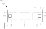
- FIG. 4 is a bottom view of the electronic device according to the first embodiment.
- FIG. 5 is a front view showing the electronic device according to the first embodiment, in which the sealing resin is indicated by imaginary lines.
- FIG. 6 is a left side view showing the electronic device according to the first embodiment, in which the sealing resin is indicated by imaginary lines.
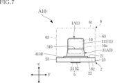
- FIG. 7 is a right side view showing the electronic device according to the first embodiment, in which the sealing resin is indicated by imaginary lines.
- FIG. 1 is a plan view showing an electronic device according to a first embodiment.
- FIG. 2 is a plan view of FIG. 1, in which the sealing resin is shown by imaginary lines.
- FIG. 3 is a plan view of FIG. 2 with
- FIG. 8 is a cross-sectional view taken along line VIII-VIII in FIG.
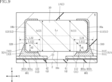
- FIG. 9 is a partially enlarged cross-sectional view of a part of FIG.
- FIG. 10 is a partially enlarged cross-sectional view of a part of FIG.
- FIG. 11 is a cross-sectional view showing a step of the method for manufacturing an electronic device according to the first embodiment, and corresponds to the cross section of FIG.
- FIG. 12 is a cross-sectional view showing a step of the method for manufacturing an electronic device according to the first embodiment, and corresponds to the cross section of FIG.
- FIG. 13 is a cross-sectional view showing a step of the method for manufacturing an electronic device according to the first embodiment, and corresponds to the cross section of FIG. FIG.
- FIG. 14 is a cross-sectional view showing a step of the method for manufacturing an electronic device according to the first embodiment, and corresponds to the cross section of FIG.
- FIG. 15 is a cross-sectional view showing a step of the method for manufacturing an electronic device according to the first embodiment, and corresponds to the cross section of FIG.
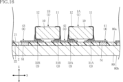
- FIG. 16 is a cross-sectional view showing a step of the method for manufacturing an electronic device according to the first embodiment, and corresponds to the cross section of FIG.
- FIG. 17 is a cross-sectional view showing a step of the method for manufacturing the electronic device according to the first embodiment, and corresponds to the cross section of FIG. FIG.
- FIG. 18 is a cross-sectional view showing a step of the method for manufacturing an electronic device according to the first embodiment, and corresponds to the cross section of FIG.
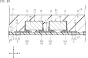
- FIG. 19 is a cross-sectional view showing a step of the method for manufacturing an electronic device according to the first embodiment, and corresponds to the cross section of FIG.
- FIG. 20 is a cross-sectional view showing an electronic device according to a first modified example of the first embodiment, and corresponds to FIG. 8 .
- FIG. 21 is a cross-sectional view showing an electronic device according to a second modified example of the first embodiment, and corresponds to FIG. 8 .
- FIG. 22 is an enlarged cross-sectional view of a main part of an electronic device according to the second embodiment, and corresponds to FIG.
- FIG. 23 is a plan view showing another configuration example of an electronic device according to the present disclosure, in which a sealing resin is indicated by imaginary lines.
- an object A is formed on an object B
- an object A is formed on (an object B)
- an object A is formed directly on an object B
- an object A is formed on an object B with another object interposed between the object A and the object B” unless otherwise specified.
- an object A is disposed on an object B” and “an object A is disposed on (an object B)” include “an object A is disposed directly on an object B” and “an object A is disposed on (an object B) with another object interposed between the object A and the object B” unless otherwise specified.
- an object A is located on (an object B) includes “an object A is in contact with an object B and is located on (an object B)” and “an object A is located on (an object B) with another object interposed between the object A and the object B".
- an object A overlaps an object B includes “an object A overlaps the entire object B” and “an object A overlaps a part of an object B” unless otherwise specified.
- An object A (its material) contains a certain material C includes “an object A (its material) is made of a certain material C” and “an object A (its material) is mainly composed of a certain material C.”
- a certain surface A faces a certain direction B (one or the other) includes, unless otherwise specified, the angle of surface A with respect to direction B is not limited to 90°, and includes the case where surface A is inclined with respect to direction B.
- An object A is perpendicular to an object B (a certain direction B) includes, unless otherwise specified, the angle of object A with respect to object B (a certain direction B) is not limited to exactly 90°, and includes the case where the angle is approximately 90° (for example, within the range of error caused by manufacturing variations).
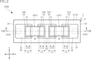
- FIGS. 1 to 10 show an electronic device A10 according to a first embodiment.
- the electronic device A10 comprises a plurality of electronic components 1, a support member 2, a plurality of conductive bonding materials 3, a wiring layer 4, a plurality of terminals 5, and a sealing resin 6.
- the electronic device A10 is surface-mounted on a circuit board of an electronic device (such as an electrical product or an electric vehicle).
- the electronic device A10 is a leadless package type.
- the shape of the electronic device A10 in a plan view is, for example, rectangular.
- the thickness direction of the electronic device A10 is referred to as the "thickness direction z.”
- one side of the thickness direction z may be referred to as the upper side, and the other side as the lower side.
- the terms “upper,” “lower,” “upper,” “lower,” “top surface,” and “bottom surface” indicate the relative positional relationship of each component, etc. in the thickness direction z, and do not necessarily define the relationship with the direction of gravity.
- “Planar view” refers to the view in the thickness direction z.
- One direction perpendicular to the thickness direction z is referred to as the "first direction x.”
- the direction perpendicular to the thickness direction z and the first direction x is referred to as the "second direction y.”
- the electronic components 1 are supported by a support member 2 as shown in FIG. 2 and FIG. 5 to FIG. 10.
- Each of the electronic components 1 is an SMD (Surface Mount Device).
- Each of the electronic components 1 is, for example, a resistor, a capacitor, an inductor, or a diode.
- Each of the electronic components 1 is a functional element of the electronic device A10.
- the electronic components 1 include two electronic components 1A and 1B. That is, the electronic device A10 includes two electronic components 1A and 1B.
- the number of electronic components 1 is not limited to two, and may be one, or may be three or more.
- the thickness (dimension in the thickness direction z) of each of the electronic components 1 (two electronic components 1A and 1B) is, for example, 200 ⁇ m or more and 1500 ⁇ m or less.
- Each of the multiple electronic components 1 (two electronic components 1A, 1B) includes a main body 10 and a pair of terminals 11, 12, as shown in Figures 2, 5, and 8.
- the main body 10 and the pair of terminals 11, 12 described below are common to each electronic component 1 (each electronic component 1A, 1B), unless otherwise specified.
- the main body 10 is the functional center of the electronic component 1, and operates as a resistor, capacitor, inductor, diode, or the like when electricity is applied to the electronic component 1. As shown in FIG. 2, in the illustrated example, the main body 10 is rectangular in plan view with its longitudinal direction aligned in the first direction x.
- the main body 10 has a pair of side surfaces 10a, 10b and a bottom surface 10c.
- the pair of side surfaces 10a, 10b are spaced apart from each other in the longitudinal direction of each electronic component 1 (first direction x in the illustrated example) and face opposite each other in the longitudinal direction of each electronic component 1 (first direction x in the illustrated example).
- the bottom surface 10c is connected to each of the pair of side surfaces 10a, 10b and is sandwiched between them.
- the bottom surface 10c faces downward in the thickness direction z and faces the support member 2.
- the main body 10 has an upper surface facing upward in the thickness direction z, a side surface facing one side in the second direction y, and a side surface facing the other side in the second direction y.
- terminal 11 is arranged at one end in the first direction x
- terminal 12 is arranged at the other end in the first direction x.
- the terminal 11 includes a side electrode 111 and a bottom electrode 112.
- the side electrode 111 covers the entire side surface 10a.
- the side electrode 111 connects from the upper (one) edge of the side surface 10a in the thickness direction z to the lower (other) edge of the side surface 10a in the thickness direction z.
- the bottom electrode 112 covers a part of the bottom surface 10c.
- the bottom electrode 112 covers the vicinity of one edge of the bottom surface 10c in the first direction x.
- the bottom electrode 112 is connected to the side electrode 111.
- the dimension L112 of the bottom electrode 112 in the first direction x i.e.
- the dimension of the terminal 11 in the first direction x) is, for example, 50 ⁇ m or more and 800 ⁇ m or less.
- the terminal 11 includes a portion covering a portion of the top surface of the main body 10, a portion of a side surface of the main body 10 facing one side of the second direction y, and a portion covering a portion of a side surface of the main body 10 facing the other side of the second direction y.
- the boundary between the side electrode 111 and the bottom electrode 112 is based on the bottom surface 10c, with the side electrode 111 on the upper side in the thickness direction z and the bottom electrode 112 on the lower side in the thickness direction z.
- the terminal 12 includes a side electrode 121 and a bottom electrode 122.
- the side electrode 121 covers the entire side surface 10b.
- the side electrode 121 connects from the upper (one) edge of the side surface 10b in the thickness direction z to the lower (other) edge of the side surface 10b in the thickness direction z.
- the bottom electrode 122 covers a part of the bottom surface 10c.
- the bottom electrode 122 covers the vicinity of the other edge of the bottom surface 10c in the first direction x.
- the bottom electrode 122 is connected to the side electrode 121.
- the dimension L122 of the bottom electrode 122 in the first direction x i.e.
- the dimension of the terminal 12 in the first direction x) is, for example, 50 ⁇ m or more and 800 ⁇ m or less.
- the terminal 12 includes a portion covering a portion of the top surface of the main body 10, a portion of a side surface facing one side of the second direction y of the main body 10, and a portion covering a portion of a side surface facing the other side of the second direction y of the main body 10.
- the boundary between the side electrode 121 and the bottom electrode 122 is based on the bottom surface 10c, with the side electrode 121 on the upper side in the thickness direction z and the bottom electrode 122 on the lower side in the thickness direction z.
- the support member 2 supports a plurality of electronic components 1 as shown in FIG. 2 and FIG. 5 to FIG. 10.
- the support member 2 includes, for example, an insulating resin.
- the insulating resin is, for example, the same as the sealing resin 6 (epoxy resin as described later), but may be different from the sealing resin 6.
- the support member 2 may include the insulating resin described above mixed with a filler such as silica.
- the support member 2 may be configured to include a single crystal intrinsic semiconductor (for example, silicon (Si)) instead of an insulating resin, may include glass, or may include ceramic.
- the planar shape of the support member 2 is, for example, rectangular as shown in FIG. 2 to FIG. 4.
- the thickness of the support member 2 (dimension along the thickness direction z) is not limited in any way, but is, for example, 30 ⁇ m or more and 300 ⁇ m or less.
- the support member 2 has a mounting surface 21, a back surface 22, and a plurality of side surfaces 23.
- the mounting surface 21 and the back surface 22 are spaced apart in the thickness direction z.
- the mounting surface 21 and the back surface 22 face opposite each other.
- the mounting surface 21 is the upper surface of the support member 2, and the back surface 22 is the lower surface of the support member 2.
- the mounting surface 21 faces the multiple electronic components 1.
- the back surface 22 faces the circuit board when the electronic device A10 is mounted on the circuit board.
- the mounting surface 21 is covered with sealing resin 6, and the back surface 22 is exposed from the sealing resin 6.
- the multiple side surfaces 23 are each sandwiched between the mounting surface 21 and the back surface 22.
- each side surface 23 in the thickness direction z is connected to the mounting surface 21, and the lower end of each side surface 23 in the thickness direction z is connected to the back surface 22.
- Each side surface 23 is flat and perpendicular to each of the mounting surface 21 and the back surface 22. As shown in Figures 2 to 4, the multiple side surfaces 23 include those facing in one direction of the first direction x, those facing in the other direction of the first direction x, those facing in one direction of the second direction y, and those facing in the other direction of the second direction y.
- the dimensional relationship between the thickness of the support member 2 (dimension in the thickness direction z) and the thickness of each electronic component 1 (dimension in the thickness direction z) is not limited in any way, but preferably the thickness of the support member 2 is 1/20 to 1/5 times the thickness of each electronic component 1.
- the thickness of the support member 2 is preferably 25 ⁇ m to 100 ⁇ m.
- the wiring layer 4 is a conductor disposed inside the electronic device A10.
- the wiring layer 4 electrically connects the multiple electronic components 1 to the multiple terminals 5.
- the wiring layer 4 is formed on the mounting surface 21 of the support member 2, as shown in FIG. 5.
- the wiring layer 4 includes a plurality of wiring portions 41, 42, and 43, as shown in Figures 2, 3, 5, and 8.
- the plurality of wiring portions 41, 42, and 43 are spaced apart from one another.
- the plurality of wiring portions 41, 42, and 43 are arranged along the first direction x.
- the wiring portion 42 is located between the wiring portion 41 and the wiring portion 42 in the first direction x.
- the wiring portion 41 is located on one side of the first direction x relative to the wiring portion 42.
- the wiring portion 41 is joined to the terminal 11 of the electronic component 1A.
- the wiring portion 41 is therefore electrically connected to the terminal 11 of the electronic component 1A.
- the wiring portion 41 is electrically connected to one of the multiple terminals 5.
- the wiring portion 42 is joined to the terminal 12 of the electronic component 1A and the terminal 11 of the electronic component 1B.
- the wiring portion 42 is therefore electrically connected to the terminal 12 of the electronic component 1A and the terminal 11 of the electronic component 1B.
- the wiring portion 43 is joined to the terminal 12 of the electronic component 1B.
- the wiring portion 43 is electrically connected to one of the multiple terminals 5.
- the wiring portion 43 is therefore electrically connected to the terminal 12 of the electronic component 1B.
- the electronic component 1A is arranged across the two wiring portions 41 and 42 in a plan view.
- the electronic component 1B is arranged across the two wiring portions 42 and 43 in a plan view.
- the wiring layer 4 (each of the multiple wiring portions 41, 42, and 43) includes a conductive layer 401, as shown in Figures 9 and 10.
- the conductive layer 401 electrically connects two parts that are spaced apart from each other, forming a conductive path between them.
- the conductive layer 401 includes a seed layer 401a and a metal layer 401b.
- the seed layer 401a is formed on the mounting surface 21.
- the seed layer 401a includes, for example, titanium (Ti).
- the metal layer 401b is laminated on the seed layer 401a.
- the metal layer 401b includes, for example, copper (Cu).
- the conductive layer 401 may be a single layer made of a conductor.
- the thickness of the conductive layer 401 (dimension in the thickness direction z) is not limited in any way, but is, for example, 10 ⁇ m or more and 100 ⁇ m or less.
- Each of the plurality of conductive bonding materials 3 bonds the wiring layer 4 to one of the plurality of electronic components 1.
- the plurality of electronic components 1 are electrically connected to the wiring layer 4 via the plurality of conductive bonding materials 3.
- Each of the plurality of conductive bonding materials 3 is a conductive bonding material.
- the plurality of conductive bonding materials 3 is, for example, solder.
- the solder contains an alloy containing tin (Sn) in its composition (for example, an Sn-silver (Ag) alloy) and contains flux.
- the composition of each of the plurality of conductive bonding materials 3 is not limited to this example.
- Each of the plurality of conductive bonding materials 3 may be a sintered metal or a conductive paste material instead of solder.
- the plurality of conductive bonding materials 3 include a pair of conductive bonding materials 31A, 32A and a pair of conductive bonding materials 31B, 32B.
- each conductive bonding material 31A, 32A is, for example, cone-shaped, and the area of a cross section perpendicular to the thickness direction z of each conductive bonding material 31A, 32A increases downward in the thickness direction z.
- each conductive bonding material 31B, 32B is, for example, cone-shaped, and the area of a cross section perpendicular to the thickness direction z of each conductive bonding material 31B, 32B increases downward in the thickness direction z.
- each conductive bonding material 31A, 31B includes an intervening portion 311 and a fillet 312.
- the intervening portion 311 and the fillet 312 are connected to each other and formed integrally.
- the intervening portion 311 of the conductive bonding material 31A is interposed between the electronic component 1A and the wiring portion 41 in the thickness direction z.
- the intervening portion 311 of the conductive bonding material 31B is interposed between the electronic component 1B and the wiring portion 42 in the thickness direction z.
- the thickness (thickness direction z) of the intervening portion 311 of each conductive bonding material 31A, 31B is not limited in any way, but is, for example, 5 ⁇ m or more and 50 ⁇ m or less.
- the fillet 312 covers a portion of the side electrode 111 of the corresponding electronic component 1A, 1B.
- the fillet 312 contacts the side electrode 111 of the corresponding electronic component 1A or 1B.
- the side surface of each fillet 312 is inclined flatly with respect to the x-y plane perpendicular to the thickness direction z, but may be curved convexly or concavely.
- each of the conductive bonding materials 31A and 31B has a peak 310.
- the fillet 312 has the peak 310.
- the peak 310 described below is common to both of the conductive bonding materials 31A and 31B unless otherwise specified.
- the top 310 is the portion of the conductive bonding material 31A, 31B located at the top in the thickness direction z.
- the distance d1 (see Figures 9 and 10) between the top 310 and the bottom surface 10c in the thickness direction z is 0 to 1/2 times (preferably 0 to 1/4 times) the dimension h111 (see Figures 9 and 10) of the lateral electrode 111 in the thickness direction z.
- the height of the conductive bonding material 31A, 31B creeping up along the lateral electrode 111 is from the lower end of the lateral electrode 111 to the center Ls (see Figures 9 and 10) of the lateral electrode 111 in the thickness direction z.
- each conductive bonding material 31A, 31B since each conductive bonding material 31A, 31B includes a fillet 312, the distance d1 is greater than 0 to 1/2 times (preferably 1/4 times) the dimension h111 of the lateral electrode 111 in the thickness direction z. In other words, in a configuration in which each conductive bonding material 31A, 31B does not include a fillet 312, the distance d1 is 0 times the thickness of the corresponding side electrode 111.
- the dimensional relationship between the dimension L31 (see Figures 2, 9, and 10) of each conductive bonding material 31A, 31B in the first direction x and the dimension L112 (see Figures 2, 9, and 10) of the bottom electrode 112 of each electronic component 1A, 1B in the first direction x is not limited in any way, but preferably, the dimension L31 of each conductive bonding material 31A, 31B in the first direction x is 1.0 to 1.5 times the dimension L112 of the bottom electrode 112 in the first direction x.
- each of the conductive bonding materials 32A and 32B includes an intervening portion 321 and a fillet 322.
- the intervening portion 321 and the fillet 322 are connected to each other and formed integrally.
- the intervening portion 321 of the conductive bonding material 32A is interposed between the electronic component 1A and the wiring portion 42 in the thickness direction z.
- the intervening portion 321 of the conductive bonding material 32B is interposed between the electronic component 1B and the wiring portion 43 in the thickness direction z.
- the thickness (thickness direction z) of the intervening portion 321 of each of the conductive bonding materials 32A and 32B is not limited in any way, but is, for example, 5 ⁇ m or more and 50 ⁇ m or less.
- the fillet 322 covers a portion of the side electrode 121 of the corresponding electronic component 1A or 1B.
- the fillet 322 contacts the side electrode 121 of the corresponding electronic component 1A or 1B.
- the side surface of each fillet 322 is inclined flatly with respect to the x-y plane perpendicular to the thickness direction z, but may be curved convexly or concavely.
- each of the conductive bonding materials 32A and 32B has a peak 320.
- the fillet 322 has the peak 320.
- the peak 320 described below is common to both of the conductive bonding materials 32A and 32B unless otherwise specified.
- the top 320 is the portion of the conductive bonding material 32A, 32B located at the top in the thickness direction z.
- the distance d2 (see Figures 9 and 10) between the top 320 and the bottom surface 10c in the thickness direction z is 0 to 1/2 times (preferably 0 to 1/4 times) the dimension h121 (see Figures 9 and 10) of the lateral electrode 121 in the thickness direction z.
- the height of the conductive bonding material 32A, 32B creeping up along the lateral electrode 121 is from the lower end of the lateral electrode 121 to the center Ls (see Figures 9 and 10) of the lateral electrode 121 in the thickness direction z.
- the distance d2 is greater than 0 to 1/2 times (preferably 1/4 times) the dimension h121 of the lateral electrode 121 in the thickness direction z.
- the distance d2 is 0 times the thickness of the side electrode 121.
- the apex 320 is at the same position as the apex 310 when viewed in the first direction x.
- the height of the conductive bonding materials 32A and 32B creeping up along the side electrode 121 is the same as the height of the conductive bonding materials 31A and 31B creeping up along the side electrode 111.
- the dimensional relationship between the dimension L32 in the first direction x of each conductive bonding material 32A, 32B (see Figures 2, 9, and 10) and the dimension L122 in the first direction x of the bottom electrode 122 of each electronic component 1A, 1B (see Figures 2, 9, and 10) is not limited in any way, but preferably, the dimension L32 in the first direction x of each conductive bonding material 32A, 32B is 1.0 to 1.5 times the dimension L122 in the first direction x of the bottom electrode 122.
- Each of the multiple terminals 5 is conductive to the wiring layer 4 and is a conductor exposed to the outside of the electronic device A10.
- Each of the multiple terminals 5 serves as a terminal when mounting the electronic device A10 on a circuit board. As shown in Figures 5 to 8, each of the multiple terminals 5 penetrates the support member 2 in the thickness direction z.
- the electronic device A10 has two terminals 5. As shown in Figure 8, one of the two terminals 5 is in contact with the wiring portion 41, and the other of the two terminals 5 is in contact with the wiring portion 43. Unlike this example, the electronic device A10 may further have a terminal 5 in contact with the wiring portion 42.
- each of the multiple terminals 5 includes a columnar portion 51 and an external electrode portion 52.
- the columnar portion 51 and external electrode portion 52 described below are common to each terminal 5 unless otherwise specified.
- the columnar portion 51 penetrates the support member 2 in the thickness direction z.
- the columnar portion 51 includes, for example, a metal material.
- the metal material is not limited to any particular material, but is, for example, Cu.
- the planar shape of the columnar portion 51 is not limited to any particular material, but is rectangular in the examples shown in FIG. 2 and FIG. 3.
- the upper surface of the columnar portion 51 (the surface facing upward in the thickness direction z) is, for example, flush with the mounting surface 21 of the support member 2.
- the upper surface of this columnar portion 51 contacts the wiring layer 4.
- the lower surface of the columnar portion 51 (the surface facing downward in the thickness direction z) is exposed from the support member 2.
- the lower surface of this columnar portion 51 is, for example, flush with the rear surface 22 of the support member 2.
- the side of the columnar portion 51 (the surface facing the first direction x or the second direction y) of all terminals 5 is covered by the support member 2, but unlike this example, some terminals 5 may have exposed sides of the columnar portion 51.
- the external electrode portion 52 contacts the portion of the columnar portion 51 that is exposed from the back surface 22 of the support member 2. As shown in FIGS. 5 to 8, the external electrode portion 52 protrudes from the back surface 22.
- the external electrode portion 52 is formed by electroless plating.
- the external electrode portion 52 is composed of multiple metal layers, for example, a Ni layer, a palladium (Pd) layer, and a gold (Au) layer stacked in this order from the side in contact with the columnar portion 51.
- the external electrode portion 52 can also be composed of multiple metal layers, such as a Ni layer and an Au layer stacked in this order from the side in contact with the columnar portion 51, or multiple metal layers, such as a Cu layer, an Ag layer, and an Sn layer stacked in this order.
- the material and forming method of the external electrode portion 52 are not limited to these examples.
- the sealing resin 6 is a synthetic resin whose main component is, for example, a black epoxy resin.
- the sealing resin 6 may contain fillers such as silica mixed into the epoxy resin.
- the sealing resin 6 covers a plurality of electronic components 1 (two electronic components 1A, 1B).
- the sealing resin 6 covers a plurality of conductive bonding materials 3 (a plurality of conductive bonding materials 31A, 31B, 32A, 32B), the wiring layer 4, and a part of the support member 2.
- the sealing resin 6 is formed on the mounting surface 21.
- the sealing resin 6 is rectangular in plan view.
- the thickness of the sealing resin 6 is not limited in any way, but is, for example, 300 ⁇ m or more and 1200 ⁇ m or less. As shown in FIG. 1 and FIG. 5 to FIG. 8, the sealing resin 6 has a resin main surface 61, a resin back surface 62, and a plurality of resin side surfaces 63.
- the resin main surface 61 and the resin back surface 62 are separated in the thickness direction z.
- the resin main surface 61 and the resin back surface 62 face opposite each other in the thickness direction z.
- the resin main surface 61 faces the same direction as the mounting surface 21 in the thickness direction z
- the resin back surface 62 faces the same direction as the back surface 22 in the thickness direction z.
- the resin back surface 62 is in contact with the mounting surface 21.
- the resin back surface 62 has projections and recesses according to the shape of the wiring layer 4.
- each of the multiple resin side surfaces 63 is sandwiched between the resin main surface 61 and the resin back surface 62 in the thickness direction z and is connected to them.
- the multiple resin side surfaces 63 are flush with a corresponding one of the multiple side surfaces 23.
- Figures 11 to 19 are cross-sectional views showing a step in the manufacturing method for electronic device A10. These cross-sectional views correspond to the cross section shown in Figure 8.
- a support substrate 80 is prepared, and a plurality of columnar portions 51 are formed on the support substrate 80.
- the support substrate 80 includes, for example, a single crystal intrinsic semiconductor material.
- the semiconductor material is, for example, Si.
- a silicon wafer is prepared as the support substrate 80.
- the support substrate 80 has a substrate main surface 80a and a substrate back surface 80b that face opposite each other in the thickness direction z.
- the plurality of columnar portions 51 are formed, for example, by the following process. First, a seed layer is formed on the substrate main surface 80a.
- the seed layer is formed, for example, by a sputtering method.
- a resist is patterned on the seed layer, and a plurality of columnar portions 51 are formed by electrolytic plating. After that, the resist layer and unnecessary seed layer are removed. Through these processes, a plurality of columnar portions 51 are formed on the substrate main surface 80a of the support substrate 80.
- a support member 2 (resin layer) that covers the multiple columnar portions 51 is formed on the substrate main surface 80a of the support substrate 80.
- the support member 2 (resin layer) is formed, for example, by molding.
- the support member 2 (resin layer) is, for example, a synthetic resin whose main component is black epoxy resin.
- the support member 2 (resin layer) may be other insulating resin material instead of the synthetic resin.
- the support member 2 (resin layer) has a mounting surface 21 and a back surface 22 that face in opposite directions in the thickness direction z.
- the mounting surface 21 faces the same direction as the substrate main surface 80a, and the back surface 22 faces the substrate main surface 80a.
- the support member 2 (resin layer) is ground.
- the support member 2 is ground downward in the thickness direction z from the mounting surface 21 until the columnar portion 51 is exposed.
- the grinding method is not particularly limited.
- the support member 2 may be made thinner by a method other than grinding.
- the wiring layer 4 is formed, for example, by the following process.
- a seed layer 401a is formed on the mounting surface 21 and each columnar portion 51.
- the seed layer 401a is formed, for example, by a sputtering method.
- a Ti layer and a Cu layer are laminated in this order as the seed layer 401a.
- a resist is patterned on the seed layer 401a, and a metal layer 401b is formed by electrolytic plating.
- the metal layer 401b contains Cu.
- the resist and unnecessary seed layer 401a (seed layer 401a exposed from the metal layer 401b) are removed.
- the wiring layer 4 (multiple wiring portions 41, 42, 43) is formed.
- a plurality of conductive bonding materials 3 (a plurality of conductive bonding materials 31A, 31B, 32A, and 32B) are formed.
- a solder paste as each conductive bonding material 3 is formed on the wiring layer 4 by screen printing.
- a plurality of electronic components 1 are mounted, and then the plurality of electronic components 1 are bonded.
- the terminal 11 of electronic component 1A and conductive bonding material 31A, the terminal 12 of electronic component 1A and conductive bonding material 32A, the terminal 11 of electronic component 1B and conductive bonding material 31B, and the terminal 12 of electronic component 1B and conductive bonding material 32B are placed in correspondence with each other. Then, reflow is performed with each electronic component 1 (each electronic component 1A, 1B) placed in the state.
- each conductive bonding material 31A, 31B, 32A, 32B melts each conductive bonding material 31A, 31B, 32A, 32B, and the fluidity of each conductive bonding material 31A, 31B, 32A, 32B becomes higher than when it is in a paste state.
- each molten conductive bonding material 31A, 31B, 32A, 32B is cooled.
- each of the conductive bonding materials 31A, 31B, 32A, and 32B solidifies, and each of the electronic components 1 (each of the electronic components 1A and 1B) is bonded.
- each of the conductive bonding materials 31A and 31B includes an intermediate portion 311 and a fillet 312.
- each of the conductive bonding materials 32A and 32B has an intermediate portion 321 and an intermediate portion 321 formed therein.
- the sealing resin 6 is formed.
- the sealing resin 6 is formed above the support member 2 so as to cover the multiple electronic components 1 and the wiring layer 4.
- the sealing resin 6 is formed, for example, by molding.
- the sealing resin 6 is a synthetic resin whose main component is, for example, a black epoxy resin.
- the sealing resin 6 may be another insulating resin material instead of the synthetic resin.
- the sealing resin 6 has a resin main surface 61 facing one side in the thickness direction z. To reduce the height of the sealing resin 6, the sealing resin 6 may be ground downward in the thickness direction z from the resin main surface 61 to such an extent that the electronic components 1 are not exposed.
- the support substrate 80 is removed.
- the support substrate 80 is ground from the rear surface 80b side of the substrate.
- the support substrate 80 is ground from the rear surface 80b side of the substrate.
- the grinding is continued even after the support substrate 80 is removed, thereby reducing the height of the support member 2 and the columnar portion 51. This reduction in height does not have to be performed.
- the external electrode portion 52 is formed.
- the external electrode portion 52 is formed on the top surface of the columnar portion 51 exposed from the rear surface 22.
- the external electrode portion 52 is formed, for example, by electroless plating. In this electroless plating, a Ni layer, a Pd layer, and an Au layer are laminated in this order from the side in contact with the columnar portion 51. In this way, a plurality of terminals 5 are formed, each of which includes a columnar portion 51 and an external electrode portion 52.
- the sealing resin 6 is cut along the cutting lines CL shown in FIG. 19 to separate the pieces.
- the sealing resin 6 is cut by cutting using, for example, a dicing blade.
- the electronic device A10 includes a conductive bonding material 31A as a first conductive bonding material.
- the conductive bonding material 31A has a topmost portion 310 as a first topmost portion.
- the distance d1 (first distance) between the topmost portion 310 and the bottom surface 10c of the main body portion 10 in the thickness direction z is 0 to 1/2 times the dimension of the lateral electrode 111 in the thickness direction z.
- the lateral electrode 111 is an example of a "first lateral electrode".
- the distance d1 is equal to or less than 1/4 times (0 times or more) the dimension of the lateral electrode 111 in the thickness direction z.
- the amount (volume) of the conductive bonding material 31A is even smaller, so the electronic device A10 is preferable in terms of reducing stress caused by the volume expansion of the conductive bonding material 31A due to a rise in temperature.
- the amount (volume) of the conductive bonding material 31A is appropriately reduced in order to reduce stress caused by volume expansion of the conductive bonding material 31A due to a rise in temperature.
- the dimension of the conductive bonding material 31A in the first direction x is 1.0 to 1.5 times the dimension L112 of the bottom electrode 112 in the first direction x.
- the bottom electrode 112 is an example of a "first bottom electrode.”
- the dimension of the conductive bonding material 31A in the first direction x is 1.0 to 1.5 times the dimension L112 of the bottom electrode 112 in the first direction x, so that the amount (volume) of the conductive bonding material 31A can be appropriately reduced while ensuring electrical continuity between the terminal 11 and the wiring portion 41.
- the other conductive bonding materials 31B, 32A, and 32B are also true for the other conductive bonding materials 31B, 32A, and 32B.
- each conductive bonding material 31A, 31B includes a fillet 312. This configuration facilitates visual inspection of whether the terminals 11 of each electronic component 1A, 1B are properly bonded to the wiring layer 4 during the manufacturing process of electronic device A10 (e.g., before the sealing resin 6 is formed).
- each conductive bonding material 32A, 32B includes a fillet 322. This configuration facilitates visual inspection of whether the terminals 12 of each electronic component 1A, 1B are properly bonded to the wiring layer 4 during the manufacturing process of electronic device A10 (e.g., before the sealing resin 6 is formed).
- the thickness of support member 2 is 1/20 to 1/5 times the thickness of each electronic component 1.
- Research by the present inventors has shown that a thinner support member 2 reduces warping of support member 2.
- a thicker support member 2 can suppress volume expansion of conductive bonding material 31A caused by a rise in temperature. Therefore, by setting the thickness of support member 2 within the above range (1/20 to 1/5), electronic device A10 can suppress volume expansion of conductive bonding material 31A caused by a rise in temperature while reducing warping of support member 2.
- the electronic device A10 includes a conductive bonding material 32A as a second conductive bonding material.
- the conductive bonding material 32A has a topmost portion 320 as a second topmost portion.
- the distance d2 (second distance) between the topmost portion 320 and the bottom surface 10c of the main body portion 10 in the thickness direction z is 0 to 1/2 times the dimension of the lateral electrode 121 in the thickness direction z.
- the lateral electrode 121 is an example of a "second lateral electrode".
- the two apexes 310, 320 for each electronic component 1A, 1B are at the same position in thickness direction z when viewed in first direction x. In other words, the two apexes 310, 320 are at the same height.
- the terminals 11 and 12 of each electronic component 1A, 1B are joined to the wiring layer 4 in the same (or approximately the same) shape, so electronic device A10 can prevent each electronic component 1A, 1B from being joined in an inclined position.
- the electronic components 1A and 1B are covered with sealing resin 6.
- the stress on the support member 2 due to the volume expansion of each conductive bonding material 3 is greater than in a configuration without sealing resin 6. This increases the possibility of cracks occurring in the support member 2.
- each conductive bonding material 3 conductive bonding materials 31A, 31B, 32A, and 32B
- each conductive bonding material 3 conductive bonding materials 31A, 31B, 32A, and 32B
- the support member 2 contains an insulating resin, and the insulating resin is the same as the constituent material of the sealing resin 6 (e.g., epoxy resin).
- the linear expansion coefficient of the support member 2 and the linear expansion coefficient of the sealing resin 6 are the same. Therefore, the electronic device A10 is able to suppress the effects of thermal stress in the electronic device A10.
- FIG. 20 shows an electronic device A11 according to a first modified example of the first embodiment.
- the electronic device A11 differs from the electronic device A10 in the following respect: each of the wiring portions 41, 42, and 43 includes a plating layer 402.
- wiring section 41 includes a conductive layer 401 and a plating layer 402
- wiring section 42 includes a conductive layer 401 and two plating layers 402
- wiring section 43 includes a conductive layer 401 and a plating layer 402.
- plating layer 402 which will be described below, is common to each of wiring sections 41, 42, and 43.
- the plating layer 402 is laminated on the conductive layer 401.
- the wettability of the plating layer 402 to each conductive bonding material 3 is higher than the wettability of the conductive layer 401 to each conductive bonding material 3.
- the plating layer 402 contains Ni.
- terminal 11 of electronic component 1A is joined to plating layer 402 of wiring portion 41 by conductive bonding material 31A
- terminal 12 of electronic component 1B is joined to one of two plating layers 402 of wiring portion 42 by conductive bonding material 32A
- terminal 11 of electronic component 1B is joined to the other of two plating layers 402 of wiring portion 42 by conductive bonding material 31B
- terminal 12 of electronic component 1B is joined to the other plating layer 402 of wiring portion 43 by conductive bonding material 32B.
- the dimension of the plating layer 402 in the first direction x is not limited in any way, but is, for example, the same (or approximately the same) as the dimension of the corresponding conductive bonding material 31A, 31B, 32A, and 32B in the first direction x.
- the dimension of each plating layer 402 in the first direction x is 1.0 to 1.5 times the dimension L112 in the first direction x of the bottom electrode 112 or the dimension L122 in the first direction x of the bottom electrode 122.
- the electronic device A11 has a conductive bonding material 31A as a first conductive bonding material, and the conductive bonding material 31A has a topmost portion 310 as a first topmost portion.
- the distance d1 (first distance) between the topmost portion 310 and the bottom surface 10c of the main body portion 10 in the thickness direction z is 0 to 1/2 times the dimension of the lateral electrode 111 in the thickness direction z.
- the electronic device A11 can reduce stress caused by volume expansion of the conductive bonding material 31A due to a rise in temperature, and can suppress the occurrence of cracks in the electronic device A11.
- the electronic device A11 has a common configuration with the electronic device A10, and thus achieves the same effects as the electronic device A10.
- each wiring portion 41, 42, 43 includes a plating layer 402, and each conductive bonding material 3 (each conductive bonding material 31A, 31B, 32A, 32B) is bonded to the corresponding plating layer 402.
- each conductive bonding material 3 each conductive bonding material 31A, 31B, 32A, 32B
- the amount (volume) of each conductive bonding material 3 is appropriately reduced in order to reduce stress caused by volume expansion of each conductive bonding material 3 due to a rise in temperature.
- the larger the planar size of each conductive bonding material 3 the smaller the dimension in the thickness direction z of the conductive bonding material 3 becomes.
- each plating layer 402 can suppress the planar size of the corresponding conductive bonding material 3 from becoming too large, so that the dimension in the thickness direction z of the conductive bonding material 3 can be appropriately secured. Therefore, the electronic device A11 can suppress insufficient thickness of each conductive bonding material 3, and therefore suppresses a decrease in the bonding strength and electrical conductivity between the terminals 11 and 12 of each electronic component 1A, 1B and the wiring layer 4. In other words, the electronic device A11 can suppress a decrease in reliability.
- the wettability of the plating layer 402 to each conductive bonding material 3 is higher than the wettability of the conductive layer 401 to each conductive bonding material 3. This configuration makes it possible to suppress outflow from the plating layer 402 to the conductive layer 401.
- both the terminal 12 of the electronic component 1A and the terminal 11 of the electronic component 1B are joined to the wiring portion 42.
- two conductive bonding materials 32A, 31B are arranged on the wiring portion 42, and if unintended leakage occurs in each of the conductive bonding materials 32A, 31B, the two conductive bonding materials 32A, 31B are integrated.
- Such integration promotes the leakage of each of the conductive bonding materials 32A, 31B, leading to insufficient thickness of each of the conductive bonding materials 32A, 31B.
- the electronic device A11 has a preferable structure in terms of suppressing a decrease in reliability.
- FIG. 21 shows an electronic device A12 according to a second modified example of the first embodiment.
- the electronic device A12 differs from the electronic device A10 in the following respect. That is, there is a step on each resin side surface 63 of the sealing resin 6 of the electronic device A12.
- each resin side surface 63 has a first side portion 631 and a second side portion 632.
- the first side portion 631 and the second side portion 632 face the same direction.
- the first side portion 631 is positioned outward from the second side portion 632.
- the first side portion 631 is connected to the resin main surface 61, and the second side portion 632 is connected to a corresponding one of the multiple side surfaces 23.
- the second side portion 632 is flush with the side surface 23 to which it is connected.
- the multiple terminals 5 include one in which the columnar portion 51 is exposed from the side surface 23.
- the external electrode portion 52 covers the surface of the columnar portion 51 exposed from the rear surface 22 of the support member 2 and the surface exposed from the side surface 23 of the support member 2.
- the electronic device A12 has a conductive bonding material 31A as a first conductive bonding material, and the conductive bonding material 31A has a topmost portion 310 as a first topmost portion.
- the distance d1 (first distance) between the topmost portion 310 and the bottom surface 10c of the main body portion 10 in the thickness direction z is 0 to 1/2 times the dimension of the lateral electrode 111 in the thickness direction z. Therefore, like the electronic device A10, the electronic device A12 can reduce stress caused by volume expansion of the conductive bonding material 31A due to a temperature rise, and can suppress the occurrence of cracks in the electronic device A12.
- the electronic device A12 has a common configuration with the electronic device A10, and thus achieves the same effects as the electronic device A10.
- each resin side surface 63 of the sealing resin 6 has a step, and due to this step, the multiple terminals 5 include those in which the columnar portion 51 is exposed from the side surface 23.
- the external electrode portion 52 is also formed on the surface of the columnar portion 51 that is exposed from the side surface 23. Therefore, when the electronic device A12 is mounted on a circuit board of an electronic device or the like, a fillet can be formed in the conductive bonding material (e.g., solder) used during the mounting. In other words, it is easier to visually inspect the electronic device A12 to determine whether it is properly bonded to the circuit board of an electronic device or the like than the electronic device A10.
- FIG. 22 shows an electronic device A20 according to the second embodiment.
- the electronic device A20 differs from the electronic device A10 in the following respects.
- the conductive bonding material 31A of the electronic device A20 does not include a fillet 312.
- the conductive bonding material 32A of the electronic device A20 does not include a fillet 322.
- the conductive bonding materials 31B, 32B are not shown, but the conductive bonding material 31B may be configured in the same manner as the conductive bonding material 31A of this modified example, or may be the same as that of the electronic device A10.
- the conductive bonding material 32B may be configured in the same manner as the conductive bonding material 32A of this modified example, or may be the same as that of the electronic device A10.
- the conductive bonding material 31A of the electronic device A20 is composed of an intervening portion 311.
- the topmost portion 310 of the conductive bonding material 31A overlaps the boundary between the side electrode 111 and the bottom electrode 112 of the terminal 11 of the electronic component 1A when viewed in the first direction x.
- the conductive bonding material 32A of the electronic device A20 is composed of an intervening portion 321.
- the topmost portion 320 of the conductive bonding material 32A overlaps the boundary between the side electrode 121 and the bottom electrode 122 of the terminal 12 of the electronic component 1A when viewed in the first direction x.
- the electronic device A20 like the electronic device A10, has a conductive bonding material 31A as a first conductive bonding material, and the conductive bonding material 31A has a topmost portion 310 as a first topmost portion.
- the distance d1 (first distance) between the topmost portion 310 and the bottom surface 10c of the main body 10 in the thickness direction z is 0 to 1/2 times the dimension of the lateral electrode 111 in the thickness direction z. Therefore, like the electronic device A10, the electronic device A20 can reduce stress caused by volume expansion of the conductive bonding material 31A due to a temperature rise, and can suppress the occurrence of cracks in the electronic device A20. This is also true for the conductive bonding material 31B.
- the electronic device A20 has a common configuration with the other electronic devices A10 to A12, and thus achieves the same effects as the electronic devices A10 to A12.
- a fillet 312 is formed in each of the conductive bonding materials 31A and 31B.
- a fillet 322 is formed in each of the conductive bonding materials 32A and 32B.
- the number of electronic components 1 was two, but in the electronic device of the present disclosure, the number of electronic components 1 may be one, or three or more.
- the electronic device may include a semiconductor element in addition to at least one electronic component 1.
- FIG. 23 shows an electronic device further including a semiconductor element 19.
- the wiring layer 4 includes a plurality of wiring parts 40, and each of the plurality of electronic components 1 is joined across any two of the plurality of wiring parts 40. This allows the plurality of electronic components 1 to be electrically connected appropriately.
- the semiconductor element 19 is, for example, an integrated circuit such as an LSI. Unlike this example, the semiconductor element 19 may be a voltage control element such as an LDO (Low Drop Out), an amplifying element such as an operational amplifier, or a discrete element such as a transistor and a diode.
- LDO Low Drop Out
- the semiconductor element 19 is flip-chip mounted across some of the plurality of wiring parts 40. This allows the semiconductor element 19 to be electrically connected appropriately to any one of the plurality of electronic components 1 and any one of the plurality of terminals 5 via at least one wiring part 40.
- the electronic device disclosed herein is not limited to those equipped with only electronic components, but also includes configurations that further include semiconductor elements.
- the electronic device is not limited to the above-described embodiment.
- the specific configuration of each part of the electronic device according to the present disclosure can be freely designed in various ways.
- the present disclosure includes the embodiments described in the following appendices.
- Appendix 1 an electronic component including a main body and a first terminal; A support member for supporting the electronic component; a wiring layer including a first wiring portion and formed on the support member; a first conductive bonding material that bonds the first terminal to the first wiring portion; Equipped with the electronic component is located on one side of the wiring layer in a thickness direction of the electronic component,
- the main body portion has a first side surface facing one side of a first direction perpendicular to the thickness direction, and a bottom surface connected to the first side surface and facing the support member,
- the first terminal includes a first side electrode covering the first side surface; the first side electrode is connected from one edge to the other edge of the first side surface in the thickness direction, the first conductive bonding material has a first top portion located on the one side in the thickness
- the first conductive bonding material includes a first intermediate portion interposed between the electronic component and the first wiring portion in the thickness direction, and a first fillet having the first top portion and connected to the first intermediate portion, 2.
- the electronic device of claim 1 wherein the first fillet covers a portion of the first side electrode.
- Appendix 3. The electronic device of claim 1, wherein the first distance is less than or equal to 1 ⁇ 4 of a dimension of the first lateral electrode in the thickness direction.
- the first terminal includes a first bottom electrode covering a portion of the bottom surface and connected to the first side electrode; 4.
- the first wiring portion includes a conductive layer laminated on the support member and a plating layer laminated on the conductive layer, The electronic device of claim 4, wherein the first conductive bonding material is in contact with the plating layer.
- Appendix 6. The electronic device of claim 5, wherein the plating layer has a higher wettability with respect to the first conductive bonding material than the conductive layer has a wettability with respect to the first conductive bonding material. Appendix 7. 7.
- a dimension of the plating layer in the first direction is 1.0 times or more and 1.5 times or less of a dimension of the first bottom electrode in the first direction.
- the main body portion has a second side surface connected to the bottom surface and facing the other side of the first direction
- the second terminal includes a second side electrode covering the second side surface
- the second side electrode is connected from one edge to the other edge of the second side surface in the thickness direction
- the second conductive bonding material has a second apex portion located on the one side in the thickness direction
- the second conductive bonding material includes a second intermediate portion interposed between the electronic component and the second wiring portion in the thickness direction, and a second fillet having the second apex and connected to the second intermediate portion, 12.
- Appendix 13 The electronic device of claim 10, wherein the second terminal includes a second bottom electrode covering a portion of the bottom surface and connected to the second side electrode.
- Appendix 14. Further comprising a sealing resin formed on the support member, 14.
- Appendix 15. covers the electronic components.
- Appendix 15. covers the electronic components.
- the sealing resin includes an epoxy resin.
- Appendix 17. 17 The electronic device of claim 16, wherein the support member includes the same material as the sealing resin.
- A10, A11, A12, A20 Electronic device 1, 1A, 1B: Electronic component 10: Main body 10a: Side 10b: Side 10c: Bottom 11, 12: Terminal 111, 121: Lateral electrode 112, 122: Bottom electrode 19: Semiconductor element 2: Support member 21: Mounting surface 22: Back surface 23: Side 3, 31A, 31B, 32A, 32B: Conductive bonding material 310, 320: Top 311, 321: Interposed portion 312, 322: Fillet 4: Wiring layer 40, 41, 42, 43: Wiring portion 401: Conductive layer 401a: Seed layer 401b: Metal layer 402: Plating layer 5: Terminal 51: Columnar portion 52: External electrode portion 6: Sealing resin 61: Resin main surface 62: Resin back surface 63: Resin side surface 631: First side portion 632: Second side portion 80: Support substrate 80a: Substrate main surface 80b: Substrate back surface CL: Cutting line
Landscapes
- Engineering & Computer Science (AREA)
- Microelectronics & Electronic Packaging (AREA)
- Manufacturing & Machinery (AREA)
- Structures Or Materials For Encapsulating Or Coating Semiconductor Devices Or Solid State Devices (AREA)
Priority Applications (2)
| Application Number | Priority Date | Filing Date | Title |
|---|---|---|---|
| JP2025527610A JPWO2024262239A1 (https=) | 2023-06-21 | 2024-05-23 | |
| US19/422,002 US20260107389A1 (en) | 2023-06-21 | 2025-12-16 | Electronic device |
Applications Claiming Priority (2)
| Application Number | Priority Date | Filing Date | Title |
|---|---|---|---|
| JP2023-101348 | 2023-06-21 | ||
| JP2023101348 | 2023-06-21 |
Related Child Applications (1)
| Application Number | Title | Priority Date | Filing Date |
|---|---|---|---|
| US19/422,002 Continuation US20260107389A1 (en) | 2023-06-21 | 2025-12-16 | Electronic device |
Publications (1)
| Publication Number | Publication Date |
|---|---|
| WO2024262239A1 true WO2024262239A1 (ja) | 2024-12-26 |
Family
ID=93935134
Family Applications (1)
| Application Number | Title | Priority Date | Filing Date |
|---|---|---|---|
| PCT/JP2024/019001 Ceased WO2024262239A1 (ja) | 2023-06-21 | 2024-05-23 | 電子装置 |
Country Status (3)
| Country | Link |
|---|---|
| US (1) | US20260107389A1 (https=) |
| JP (1) | JPWO2024262239A1 (https=) |
| WO (1) | WO2024262239A1 (https=) |
Citations (8)
| Publication number | Priority date | Publication date | Assignee | Title |
|---|---|---|---|---|
| JPH0533568U (ja) * | 1991-10-03 | 1993-04-30 | 三菱電機株式会社 | リードレス部品実装構造 |
| JPH06163305A (ja) * | 1992-11-25 | 1994-06-10 | Sony Corp | チップ部品 |
| JP2000244105A (ja) * | 1999-02-23 | 2000-09-08 | Denso Corp | 電子部品の実装構造 |
| JP2005251904A (ja) * | 2004-03-03 | 2005-09-15 | Denso Corp | 基板表面実装部品、基板回路、基板、ハンダ接続方法、及び基板回路の製造方法 |
| JP2011009397A (ja) * | 2009-06-25 | 2011-01-13 | Fujikura Ltd | 電子部品実装配線基板 |
| WO2017115441A1 (ja) * | 2015-12-28 | 2017-07-06 | オリンパス株式会社 | 実装構造体、撮像装置および内視鏡 |
| JP2018014381A (ja) * | 2016-07-20 | 2018-01-25 | 富士通株式会社 | 基板及び電子機器 |
| JP2021072434A (ja) * | 2019-10-30 | 2021-05-06 | 新光電気工業株式会社 | 半導体装置及び半導体装置の製造方法 |
-
2024
- 2024-05-23 WO PCT/JP2024/019001 patent/WO2024262239A1/ja not_active Ceased
- 2024-05-23 JP JP2025527610A patent/JPWO2024262239A1/ja active Pending
-
2025
- 2025-12-16 US US19/422,002 patent/US20260107389A1/en active Pending
Patent Citations (8)
| Publication number | Priority date | Publication date | Assignee | Title |
|---|---|---|---|---|
| JPH0533568U (ja) * | 1991-10-03 | 1993-04-30 | 三菱電機株式会社 | リードレス部品実装構造 |
| JPH06163305A (ja) * | 1992-11-25 | 1994-06-10 | Sony Corp | チップ部品 |
| JP2000244105A (ja) * | 1999-02-23 | 2000-09-08 | Denso Corp | 電子部品の実装構造 |
| JP2005251904A (ja) * | 2004-03-03 | 2005-09-15 | Denso Corp | 基板表面実装部品、基板回路、基板、ハンダ接続方法、及び基板回路の製造方法 |
| JP2011009397A (ja) * | 2009-06-25 | 2011-01-13 | Fujikura Ltd | 電子部品実装配線基板 |
| WO2017115441A1 (ja) * | 2015-12-28 | 2017-07-06 | オリンパス株式会社 | 実装構造体、撮像装置および内視鏡 |
| JP2018014381A (ja) * | 2016-07-20 | 2018-01-25 | 富士通株式会社 | 基板及び電子機器 |
| JP2021072434A (ja) * | 2019-10-30 | 2021-05-06 | 新光電気工業株式会社 | 半導体装置及び半導体装置の製造方法 |
Also Published As
| Publication number | Publication date |
|---|---|
| US20260107389A1 (en) | 2026-04-16 |
| JPWO2024262239A1 (https=) | 2024-12-26 |
Similar Documents
| Publication | Publication Date | Title |
|---|---|---|
| US8339797B2 (en) | Package substrate | |
| CN100562999C (zh) | 电路模块 | |
| JP7179526B2 (ja) | 半導体装置および半導体装置の製造方法 | |
| US10334740B2 (en) | Electronic-component mount substrate, electronic device, and electronic module | |
| WO2024262239A1 (ja) | 電子装置 | |
| KR102787140B1 (ko) | 반도체 패키지 및 이의 제조방법 | |
| JP7022541B2 (ja) | 半導体装置 | |
| JP5178028B2 (ja) | 半導体装置の製造方法 | |
| JP3652102B2 (ja) | 電子回路モジュール | |
| WO2024262253A1 (ja) | 電子装置 | |
| JP2014078627A (ja) | 配線基板、はんだバンプ付き配線基板および半導体装置 | |
| US20250318053A1 (en) | Electronic device and method for manufacturing electronic device | |
| JP7382167B2 (ja) | 電子装置、および電子装置の製造方法 | |
| US20260107814A1 (en) | Electronic device | |
| JP7154818B2 (ja) | 半導体装置および半導体装置の製造方法 | |
| WO2024176756A1 (ja) | 電子装置 | |
| WO2024209909A1 (ja) | 電子装置 | |
| EP1093165A1 (en) | Integrated circuit assembly | |
| US20260005157A1 (en) | Electronic device | |
| WO2024209917A1 (ja) | 電子装置 | |
| JPH10173083A (ja) | 電子部品搭載用配線基板とその製造方法 | |
| US20250293124A1 (en) | Semiconductor device and method for manufacturing the same | |
| JP2024051292A (ja) | 半導体装置 | |
| JP2012080145A (ja) | 半導体装置 | |
| WO2024209902A1 (ja) | 電子装置 |
Legal Events
| Date | Code | Title | Description |
|---|---|---|---|
| 121 | Ep: the epo has been informed by wipo that ep was designated in this application |
Ref document number: 24825646 Country of ref document: EP Kind code of ref document: A1 |
|
| ENP | Entry into the national phase |
Ref document number: 2025527610 Country of ref document: JP Kind code of ref document: A |
|
| WWE | Wipo information: entry into national phase |
Ref document number: 2025527610 Country of ref document: JP |
|
| NENP | Non-entry into the national phase |
Ref country code: DE |