WO2024257796A1 - リードフレーム材およびその製造方法、ならびに半導体パッケージ - Google Patents
リードフレーム材およびその製造方法、ならびに半導体パッケージ Download PDFInfo
- Publication number
- WO2024257796A1 WO2024257796A1 PCT/JP2024/021338 JP2024021338W WO2024257796A1 WO 2024257796 A1 WO2024257796 A1 WO 2024257796A1 JP 2024021338 W JP2024021338 W JP 2024021338W WO 2024257796 A1 WO2024257796 A1 WO 2024257796A1
- Authority
- WO
- WIPO (PCT)
- Prior art keywords
- coating
- lead frame
- frame material
- surface coating
- alloy
- Prior art date
- Legal status (The legal status is an assumption and is not a legal conclusion. Google has not performed a legal analysis and makes no representation as to the accuracy of the status listed.)
- Ceased
Links
Images


Classifications
-
- C—CHEMISTRY; METALLURGY
- C25—ELECTROLYTIC OR ELECTROPHORETIC PROCESSES; APPARATUS THEREFOR
- C25D—PROCESSES FOR THE ELECTROLYTIC OR ELECTROPHORETIC PRODUCTION OF COATINGS; ELECTROFORMING; APPARATUS THEREFOR
- C25D5/00—Electroplating characterised by the process; Pretreatment or after-treatment of workpieces
- C25D5/60—Electroplating characterised by the structure or texture of the layers
-
- C—CHEMISTRY; METALLURGY
- C25—ELECTROLYTIC OR ELECTROPHORETIC PROCESSES; APPARATUS THEREFOR
- C25D—PROCESSES FOR THE ELECTROLYTIC OR ELECTROPHORETIC PRODUCTION OF COATINGS; ELECTROFORMING; APPARATUS THEREFOR
- C25D3/00—Electroplating: Baths therefor
- C25D3/02—Electroplating: Baths therefor from solutions
- C25D3/12—Electroplating: Baths therefor from solutions of nickel or cobalt
-
- C—CHEMISTRY; METALLURGY
- C25—ELECTROLYTIC OR ELECTROPHORETIC PROCESSES; APPARATUS THEREFOR
- C25D—PROCESSES FOR THE ELECTROLYTIC OR ELECTROPHORETIC PRODUCTION OF COATINGS; ELECTROFORMING; APPARATUS THEREFOR
- C25D3/00—Electroplating: Baths therefor
- C25D3/02—Electroplating: Baths therefor from solutions
- C25D3/38—Electroplating: Baths therefor from solutions of copper
-
- C—CHEMISTRY; METALLURGY
- C25—ELECTROLYTIC OR ELECTROPHORETIC PROCESSES; APPARATUS THEREFOR
- C25D—PROCESSES FOR THE ELECTROLYTIC OR ELECTROPHORETIC PRODUCTION OF COATINGS; ELECTROFORMING; APPARATUS THEREFOR
- C25D5/00—Electroplating characterised by the process; Pretreatment or after-treatment of workpieces
- C25D5/10—Electroplating with more than one layer of the same or of different metals
-
- C—CHEMISTRY; METALLURGY
- C25—ELECTROLYTIC OR ELECTROPHORETIC PROCESSES; APPARATUS THEREFOR
- C25D—PROCESSES FOR THE ELECTROLYTIC OR ELECTROPHORETIC PRODUCTION OF COATINGS; ELECTROFORMING; APPARATUS THEREFOR
- C25D7/00—Electroplating characterised by the article coated
-
- H—ELECTRICITY
- H10—SEMICONDUCTOR DEVICES; ELECTRIC SOLID-STATE DEVICES NOT OTHERWISE PROVIDED FOR
- H10W—GENERIC PACKAGES, INTERCONNECTIONS, CONNECTORS OR OTHER CONSTRUCTIONAL DETAILS OF DEVICES COVERED BY CLASS H10
- H10W70/00—Package substrates; Interposers; Redistribution layers [RDL]
- H10W70/40—Leadframes
- H10W70/456—Materials
- H10W70/457—Materials of metallic layers on leadframes
-
- H—ELECTRICITY
- H10—SEMICONDUCTOR DEVICES; ELECTRIC SOLID-STATE DEVICES NOT OTHERWISE PROVIDED FOR
- H10W—GENERIC PACKAGES, INTERCONNECTIONS, CONNECTORS OR OTHER CONSTRUCTIONAL DETAILS OF DEVICES COVERED BY CLASS H10
- H10W72/00—Interconnections or connectors in packages
Definitions
- resin-sealed semiconductor devices are incorporated into electronic and electrical devices. These resin-sealed semiconductor devices are made by sealing a semiconductor element and a lead frame material, which are electrically connected to each other by wires or the like, with a molded resin. In such resin-sealed semiconductor devices, the lead frame material is often externally plated with Au, Ag, Sn, etc. to impart functionality such as bonding, heat resistance, and sealing properties.
- leadframe materials pre-plated leadframes
- a plating e.g. Ni/Pd/Au
- soldering designed to increase wettability with solder when mounted on a printed circuit board by soldering
- the adhesion of the molded resin to the lead frame material is improved, making it possible to prevent peeling between the lead frame material and the molded resin, improving the reliability of the resin-encapsulated semiconductor device.
- the resin adhesion of the lead frame material is certainly improved compared to the conventional method.
- the pass level for airtightness of the package will become stricter. For example, when a heat cycle test was performed in which a heat cycle assuming a harsh usage environment, for example, a cycle of holding at -50°C for 30 minutes and then holding at 105°C for 30 minutes was repeated 50 times, a gap was generated between the resin and the lead frame, and the airtightness of the package was reduced, which may cause defects.
- Patent Document 1 a 0.001-0.1 ⁇ m thick Au plating film is formed on a Pd or Pd alloy film formed on the outer lead of the lead frame to improve the mounting characteristics of the lead frame, but the lead frame material has low adhesion to the molded resin, so peeling is likely to occur at the interface with the molded resin.
- the crystal orientation of at least the top or side of the lead frame material is controlled to form a group of needle-like protrusions to improve adhesion between the lead frame material and the molded resin, but in high-temperature environments or environments subject to thermal shock, peeling of the molded resin from the side, where the adhesive area with the molded resin is small, is likely to occur.
- the roughening particle protrusions are shaped so that the maximum width measured on the cross section in the thickness direction of the roughening film is 1-5 times the minimum width measured on the lower part located on the conductive base side from the measurement position of the maximum width, thereby improving adhesion with the molded resin, but further improvement is required for the airtightness of the package when a more severe usage environment is assumed.
- the object of the present invention is to provide a lead frame material and a manufacturing method thereof, as well as a semiconductor package using the same, which can improve the airtightness of the package and is less likely to cause powder fall even when subjected to heat cycles that simulate harsh usage environments.
- the present inventors have focused on the fact that in a lead frame material having a surface coating formed on at least one or both of the front and back surfaces of at least a part of a base, and a side coating adjacent to the surface coating and formed on at least a part of the side surface of the base, the adhesiveness to the resin after a heat cycle changes by controlling the average roughness height of the surface coating and the side coating, and thereby the airtightness of the package changes.
- the average roughness height of the surface coating is h 1 and the average roughness height of the side coating is h 2
- the ratio h 2 /h 1 of the average roughness height h 2 of the side coating to the average roughness height h 1 of the surface coating is 1.35 or more
- the gist of the present invention is as follows.
- a leadframe material having a conductive base, a surface coating formed on one or both of at least a portion of the front and back surfaces of the base, and a side coating adjacent to the surface coating and formed on at least a portion of the side surface of the base, wherein the surface coating and the side coating both have roughened upper surfaces, and when the average roughness height of the surface coating is h1 and the average roughness height of the side coating is h2 , the ratio h2 / h1 of the average roughness height h2 of the side coating to the average roughness height h1 of the surface coating is 1.35 or greater.
- a lead frame material described in any one of (7) to (9) above, wherein the surface coating and the side coating further have at least one surface coating layer formed on the upper surface of the roughened layer.
- the present invention provides a lead frame material and a manufacturing method thereof, as well as a semiconductor package using the same, which can improve the airtightness of the package and reduce the risk of powder falling off, even when subjected to heat cycles that simulate harsh usage environments.
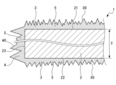
- FIG. 1 is a schematic cross-sectional view showing a portion of a lead frame material according to an embodiment of the present invention.
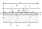
- FIG. 2 is a cross-sectional view showing a surface coating formed on the surface of a base of a lead frame material having the same configuration as FIG. 1, and is a diagram for explaining the relationship between the upper surface of the surface coating and virtual lines l1 and n1 , and the relationship between virtual line m1 and average roughness height h1 of the surface coating.
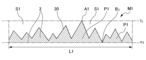
- FIG. 3 is a cross-sectional view showing an evaluation area M1 in a surface coating having the same configuration as FIG.
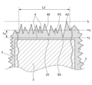
- FIG. 2 is a cross-sectional view showing a side coating formed on a side surface of a substrate of a lead frame material having the same configuration as FIG. 1, and is a diagram for explaining the relationship between the upper surface of the surface coating and virtual lines l2 and n2 , and the relationship between virtual line m2 and average roughness height h2 of the surface coating.
- 5 is a cross-sectional view showing an evaluation area M2 in a side coating having the same configuration as in FIG.
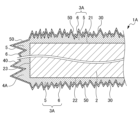
- FIG. 4 is a cross-sectional view showing an outline of a lead frame material according to another embodiment of the present invention.
- FIG. 2 is a schematic diagram showing the positional relationship between a lead frame material and a resin in measuring adhesion between the lead frame material and the resin according to an example of the present invention.
- 1 is a secondary electron image of a cross section of the lead frame material of Example 1 of the present invention observed by an SEM.
- Fig. 1 is a cross-sectional view showing an outline of a lead frame material according to an embodiment of the present invention.
- the lead frame material 1 of the present invention has a conductive base 2, a surface coating 3 formed on at least one or both of the front surface 21 and the back surface 22 of the base 2, and a side coating 4 adjacent to the surface coating 3 and formed on at least a part of the side surface 23 of the base 2, and both the surface coating 3 and the side coating 4 have roughened upper surfaces 30, 40.
- the ratio h 2 /h 1 of the average roughness height h 2 of the side coating 4 to the average roughness height h 1 of the surface coating 3 is 1.35 or more.
- the average roughness heights h1 and h2 of the surface coating 3 and the side coating 4 it is possible to change the adhesion of the lead frame material 1 to the resin after the heat cycle and the airtightness of the package.
- the average roughness height h2 of the side coating 4 larger relative to the average roughness height h1 , the adhesion of the side coating 4 to the molded resin, which has been low in the past due to a small contact area with the molded resin, can be increased relative to the adhesion of the surface coating 3 to the molded resin, thereby improving the airtightness of the package.
- the average roughness height h1 of the surface coating 3 is large, powder falling from the surface coating 3 becomes more likely to occur, so by making the average roughness height h2 of the side coating 4 larger relative to the average roughness height h1 , it is possible to make powder falling less likely to occur.
- a lead frame material capable of improving the airtightness of the package can be obtained even when subjected to a heat cycle assuming a severe usage environment by setting the ratio h2 / h1 of the average roughness height h2 of the side coating 4 to the average roughness height h1 of the surface coating 3 to 1.35 or more. Furthermore, the lead frame material 1 according to the present invention in which the ratio h2 / h1 of the average roughness height h2 of the side coating 4 to the average roughness height h1 of the surface coating 3 is 1.35 or more is also excellent in that powder falling is less likely to occur.
- the average roughness heights h1 , h2 of the surface coating 3 and the side coating 4 can be controlled, for example, by forming the roughened layer 5 of the surface coating 3 and the side coating 4 by electroplating (roughening plating), and by installing a shielding plate between the surface 21 of the base 2 and a counter electrode when performing the electroplating (roughening plating), adjusting the aperture ratio of the shielding plate, and adjusting the current density in the range of 5 A/dm2 or more and 80 A/dm2 or less.
- the lead frame material 1 of the present invention has a conductive base 2, a surface coating 3 formed on one or both of at least a portion of the front surface 21 and back surface 22 of the base 2, and a side coating 4 adjacent to the surface coating 3 and formed on at least a portion of the side surface 23 of the base 2.
- the base 2 is made of a metal or alloy containing copper (Cu), iron (Fe) or aluminum (Al). More specifically, from the viewpoint of improving electrical conductivity and heat dissipation, it is preferable that the base 2 is made of copper, a copper alloy, iron, an iron alloy, aluminum or an aluminum alloy.
- the alloy composition is not particularly limited and can be selected appropriately depending on the characteristics required of the lead frame material.
- copper alloys that make up the base 2 include pure copper (oxygen-free copper (OFC): C1020 or tough pitch copper (TPC): C1100, etc.), as well as C18045 (Cu-0.3Cr-0.25Sn-0.52Zn) and C19400 (Cu-2.3Fe-0.03P-0.15Zn), which are alloys listed in the Copper Development Association (CDA).
- An example of an iron alloy that makes up the base 2 is 42 alloy (Fe-42Ni). The number before each element indicates the content in mass% in the alloy.
- the substrate 2 is preferably in the form of a metal foil or alloy foil, and examples of such metal foil or alloy foil include rolled foil and electrolytic foil.
- rolled foil formed by press processing or the like may be used for the substrate 2.
- the thickness of the substrate 2 is not particularly limited, but is, for example, in the range of 1 ⁇ m to 500 ⁇ m, preferably 5 ⁇ m to 200 ⁇ m.
- the surface coating 3 is a coating formed on one or both of the front surface 21 and the back surface 22 of at least a portion of the base 2.
- the side surface coating 4 is a coating adjacent to the surface coating 3 and formed on at least a portion of the side surface 23 of the base 2. Therefore, the lead frame material 1 of the present invention has the above-mentioned conductive base 2, the surface coating 3, and the side surface coating 4.
- the surface coating 3 and the side coating 4 both have roughened upper surfaces 30, 40, and when the average roughness height of the upper surface 30 of the surface coating 3 is h 1 and the average roughness height of the upper surface 40 of the side coating 4 is h 2 , the ratio h 2 /h 1 of the average roughness height h 2 of the side coating 4 to the average roughness height h 1 of the surface coating 3 is 1.35 or more.
- the roughness of the side coating 4 formed on the side surface 23 of the base 2 is greater than that of the surface coating 3 formed on the front surface 21 and back surface 22 of the base 2, so that gaps are less likely to occur between the side coating 4 and the resin (molding resin) on the side surface 23 of the base 2.
- the ratio h2 / h1 of the average roughness height h2 of the side coating 4 to the average roughness height h1 of the surface coating 3 is less than 1.35, the adhesion of the side coating 4 to the resin is significantly reduced compared to the adhesion of the surface coating 3 to the resin, so that gaps are more likely to occur between the side surface 23 of the substrate 2 and the resin during a heat cycle, reducing the airtightness of the package.
- the ratio h2 / h1 of the average roughness height h2 of the side coating 4 to the average roughness height h1 of the surface coating 3 is preferably in the range of 1.35 to 5.00, and more preferably in the range of 1.66 to 5.00.
- the average roughness height h1 of the surface coating 3 is preferably in the range of 0.5 ⁇ m to 3.5 ⁇ m, and more preferably in the range of 0.8 ⁇ m to 2.5 ⁇ m.
- the average roughness height h1 of the surface coating 3 is preferably 0.5 ⁇ m or more, and more preferably 0.8 ⁇ m or more.
- the average roughness height h1 of the surface coating 3 is preferably 3.5 ⁇ m or less, and more preferably 2.5 ⁇ m or less.
- the average roughness height h2 of the side coating 4 is preferably in the range of 1.0 ⁇ m or more and 6.5 ⁇ m or less, and more preferably in the range of 1.2 ⁇ m or more and 4.8 ⁇ m or less.
- the average roughness height h2 of the side coating 4 is preferably 1.0 ⁇ m or more, more preferably 1.2 ⁇ m or more, and even more preferably 1.5 ⁇ m or more.
- the average roughness height h2 of the side coating 4 is preferably 6.5 ⁇ m or less, and more preferably 4.8 ⁇ m or less.
- the average roughness height h1 of the surface coating 3 and the average roughness height h2 of the side coating 4 can be determined by observing microtomed cross sections of the surface coating 3 and the side coating 4 including the thickness direction using a scanning electron microscope (SEM).
- SEM scanning electron microscope
- three fields of view are randomly selected for each of the surface coating 3 formed on the front surface 21, the surface coating 3 formed on the back surface 22, and the side coating 4 formed on the side surface 23, with ten continuous irregularities in the coating being one field of view.
- an evaluation area (evaluation area M1 for the surface coating 3 or evaluation area M2 for the side coating 4) is defined by an imaginary line drawn parallel to the front surface (or back surface or side surface) of the substrate 2 passing through the highest point of the irregularity (the highest point of the upper surface of the coating) and an imaginary line drawn parallel to the front surface (or back surface or side surface) of the substrate 2 passing through the lowest point of the irregularity (the lowest point of the upper surface of the coating).
- the area occupied by the surface coating 3 or the side coating 4 presence area P1 of the surface coating 3, presence area P2 of the side coating 4) can be calculated.
- the area of the portion occupied by the surface coating 3 or the side coating 4 can be calculated using image processing software ImageJ by setting the lower threshold to 128 and the upper threshold to 255, respectively, and performing binarization processing to fill in the interior of the area where the surface coating 3 and the side coating 4 are present while excluding separation points in the binarization setting.
- the value obtained by dividing the area of the portion occupied by the surface coating 3 or the side coating 4 obtained at this time by the length of the line segment (the width of 10 irregularities) can be used as the average roughness height of the coating (surface coating 3 or side coating 4) for each field of view.
- a virtual line l 1 is drawn parallel to the surface 21 passing through the highest point A1 of the upper surface 30 of the surface coating 3
- a virtual line n 1 is drawn parallel to the surface 21 passing through the lowest point B1 of the upper surface of the surface coating 3 for each visual field.
- the area partitioned by the virtual line l 1 and the virtual line n 1 is set as an evaluation area M1, and the area of the portion of these evaluation areas M1 occupied by the surface coating 3 can be calculated to calculate the area of the presence region P1 of the surface coating 3 in the evaluation area M1 on the surface 21.
- the area of the presence region P1 of the surface coating 3 in the evaluation area M1 on the back surface 22 can be calculated in the same manner.
- the value obtained by dividing the area of the presence region P1 of the surface coating 3 obtained at this time by the length of the line segment (the width of 10 irregularities) L1 can be used as the average roughness height of the surface coating 3 for each visual field.
- the average of the average roughness heights of the surface coating 3 for a total of six visual fields that is, three visual fields on the front surface 21 side and three visual fields on the back surface 22 side
- the average roughness height h1 of the surface coating 3 can be taken as the average roughness height h1 of the surface coating 3.
- a virtual line l 2 is drawn parallel to the side 23 passing through the highest point A2 of the upper surface 40 of the side coating 4
- a virtual line n 2 is drawn parallel to the side 23 passing through the lowest point B2 of the upper surface of the side coating 4 for each visual field.
- the area partitioned by the virtual line l 2 and the virtual line n 2 is set as the evaluation area M2, and the area of the presence region P2 of the side coating 4 occupying in these evaluation areas M2 can be calculated to calculate the area of the presence region P2 of the side coating 4 occupying in the evaluation area M2 on the side 23.
- the value obtained by dividing the area of the presence region P2 of the side coating 4 obtained at this time by the length of the line segment (width of 10 irregularities) L2 can be used as the average roughness height of the side coating 4 for each visual field. Furthermore, the average roughness height h 2 of the side coating 4 can be obtained by taking the average of the average roughness heights of the side coating 4 for the three visual fields in which the side coating 4 is formed.
- FIG. 2 is a cross-sectional view showing the surface coating 3 formed on the surface 21 of the base 2 of a lead frame material 1 having the same configuration as FIG. 1, but for convenience in explaining the surface coating presence region P1, the portion of the surface coating 3 included in the evaluation area M1 (the portion included in the surface coating presence region P1) and the portion not included in the evaluation area M1 (the portion not included in the surface coating presence region P1 in the evaluation area M1) are hatched differently.
- FIG. 4 is a cross-sectional view showing the side coating 4 formed on the side 23 of the base 2 of a lead frame material 1 having the same configuration as FIG. 1, but for convenience in explaining the surface coating presence region P2, the portion of the side coating 4 included in the evaluation area M2 and the portion not included in the evaluation area M2 are hatched differently.
- a first porosity in a first measurement area (e.g., the area of the above-mentioned evaluation area M1) defined by an imaginary line l 1 passing through the position of the highest point A1 of the upper surface 30 of the surface coating 3 and drawn parallel to the surface 21 (or back surface 22) of the substrate 2 and an imaginary line n 1 passing through the position of the lowest point B1 of the upper surface 30 of the surface coating 3 and drawn parallel to the surface 21 of the substrate 2 is defined as V 1
- a second porosity in a second measurement area (e.g., the area of the above-mentioned evaluation area M2) defined by an imaginary line l 2 passing through the position of the highest point A2 of the upper surface 40 of the side coating 4 and drawn parallel to the side surface 23 of the substrate 2 and an imaginary line n 2 passing through the position of the lowest point B2 of the upper surface 40 of the side coating 4 and drawn parallel to the side surface 23 of the substrate 2 is defined as
- the ratio V2 / V1 of 2 is preferably in the range of 0.50 or more and 0.91 or less.
- V2 / V1 is less than 0.50, the adhesion of the side surface 23 to the resin is weaker than that of the front surface 21 and the back surface 22, and the airtightness of the package when sealed with resin is reduced when subjected to a heat cycle assuming a harsh usage environment, compared to when V2 / V1 is 0.50 or more, and the heat cycle resistance is reduced.
- the ratio V2 / V1 of the second porosity V2 to the first porosity V1 is preferably in the range of 0.50 or more and 0.91 or less, and more preferably in the range of 0.62 or more and 0.83 or less.
- the resin and the lead frame material 1 have different thermal expansion coefficients, and the resin undergoes a larger volume change due to heat than the lead frame material 1. Therefore, it is preferable to control the ratio of the space for the resin to enter in the portion where the resin and the lead frame material 1 can contact each other, that is, the porosity of the surface coating 3 and the side coating 4 of the lead frame material 1, within an appropriate range. More specifically, it is preferable that the first porosity V1 and the second porosity V2 are both in the range of 32% to 64%.
- the resin is less likely to enter the unevenness of the upper surface 30, 40 of the surface coating 3 or the side coating 4, and therefore, compared to when these porosities are 32% or more, a gap may be generated between the lead frame material 1 and the resin, resulting in a decrease in adhesion.
- the lead frame material 1 may not be able to follow the expansion and contraction of the resin, and therefore, when subjected to a heat cycle assuming a severe usage environment, the resin is more likely to peel off from the lead frame material 1, and the adhesion between the resin and the lead frame material 1 decreases, and the airtightness of the package decreases, thereby decreasing the heat cycle resistance, compared to when the porosity is 32% or more.
- the adhesion between the lead frame material 1 and the resin may decrease, compared to when the porosity is 64% or less.
- the pressure applied to the surface coating 3 and the side coating 4 increases when the resin expands due to heating, and when this is repeated by a heat cycle, the surface coating 3 and the side coating 4 are likely to be damaged and gaps are likely to occur.
- the first porosity V1 is preferably in the range of 32% to 64%, and more preferably in the range of 45% to 60%.
- the second porosity V2 is preferably in the range of 32% to 64%, more preferably in the range of 32% to 52%, and even more preferably in the range of 35% to 50%.
- the first porosity V1 and the second porosity V2 can be obtained by using the SEM images used to measure the average roughness height h1 of the surface coating 3 and the average roughness height h2 of the side coating 4 to calculate the ratio of the void area obtained by subtracting the area of the coating portion P from the area of the evaluation areas M1 , M2 to the total area of the evaluation areas M1, M2 for each of the surface coating 3 formed on the front surface 21, the surface coating 3 formed on the back surface 22, and the side coating 4 formed on the side surface 23, thereby obtaining the porosity for each field of view.
- the average of the porosities of the surface coating 3 for a total of six fields of view can be taken as the first porosity V1 (%).
- the average of the porosities of the surface coating 3 for three fields of view on the side on which the surface coating 3 is formed can be taken as the first porosity V1 .
- the average of the porosities for three fields of view can be taken as the second porosity V2 (%).
- the ratio of the thickness T of the base 2 to the average roughness height h2 of the side coating 4 is preferably in the range of 15.0 to 200.0.
- the T/ h2 ratio is smaller than 15.0, the roughness height of the side coating 4 becomes excessively large relative to the area of the side surface 23 of the base 2, so that powder fall is more likely to occur than when the T/ h2 ratio is 15.0 or more.
- the ratio of the thickness T of the base 2 to the average roughness height h2 of the side coating 4 is preferably in the range of 15.0 to 200.0, and more preferably in the range of 20.0 to 125.0.
- the surface coating 3 and the side coating 4 are each formed by a roughened layer 5.
- the surface coating 3A and the side coating 4A which have the surface coating layer 6, are formed by a roughened layer 5 and a surface coating layer 6.
- the roughened layer 5 is formed on at least a portion of the surface of the substrate 2.
- the roughened layer 5 is formed by adhering roughening particles to the surface 21, rear surface 22, or side surface 23 of the substrate 2.
- the roughened layer 5 is preferably made of a metal or alloy containing at least one of copper (Cu) and nickel (Ni). More specifically, from the viewpoint of forming a roughened shape with excellent adhesion to resin, the roughened layer 5 is preferably made of copper, a copper alloy, nickel, or a nickel alloy.
- the roughened layer 5 can be formed by, for example, electroplating, focused ion beam (FIB), or mechanical polishing. Among these, it is particularly preferable that the roughened layer 5 is formed as an electroplated layer by electroplating.
- FIB focused ion beam
- the surface coating 3A and the side coating 4A preferably further have at least one surface coating layer 6 formed on the upper surface 50 of the roughened layer 5.
- the surface coating 3A and the side coating 4A which are the measurement targets for the average roughness height h 1 of the surface coating 3 and the average roughness height h 2 of the side coating 4, have the roughened layer 5 and the surface coating layer 6 formed on at least the surface of the roughened layer 5.
- the adhesion to the resin is increased depending on the surface properties of the roughened layer 5, and the composition of the surface of the lead frame material 1A changes, so that it is possible to increase both the wettability with the solder and the adhesion to the resin while improving the adhesion to the base 2.
- the presence or absence of a surface coating layer 6 and the number of surface coating layers 6 are appropriately selected depending on the application of the lead frame material.
- At least one of the surface coating layers 6 is preferably composed of a metal or alloy layer having a different composition from the roughening layer 5. More specifically, at least one of the surface coating layers 6 is preferably composed of a metal or alloy containing one or more elements selected from the group consisting of copper (Cu), nickel (Ni), cobalt (Co), palladium (Pd), rhodium (Rh), ruthenium (Ru), platinum (Pt), iridium (Ir), gold (Au), silver (Ag), tin (Sn) and indium (In).
- At least one of the surface coating layers 6 is preferably composed of copper, copper alloy, nickel, nickel alloy, cobalt, cobalt alloy, palladium, palladium alloy, rhodium, rhodium alloy, ruthenium, ruthenium alloy, platinum, platinum alloy, iridium, iridium alloy, gold, gold alloy, silver, silver alloy, tin, tin alloy, indium or indium alloy.
- the surface coating layer 6 is the surface that comes into contact with the outside of the lead frame material 1A, and it is preferable that it has excellent wettability with solder, etc. Therefore, the surface coating layer 6 is preferably made of a metal or alloy containing one or more elements selected from the group consisting of gold (Au), silver (Ag), copper (Cu) and tin (Sn). In particular, from the viewpoint of improving wettability with solder, the surface coating layer 6 is preferably made of a gold-cobalt alloy, gold, silver, copper or tin.
- the thickness of the surface coating layer 6 is not particularly limited, but if the thickness is too large, the unevenness formed in the roughened layer 5 may be filled in, which may at least partially impair the effect of improving the resin adhesion. Therefore, the thickness of the surface coating layer 6 is preferably 3.00 ⁇ m or less. Furthermore, when the surface coating layer 6 is made of a metal or alloy containing a precious metal such as gold or silver, it is more preferable that the thickness of the surface coating layer 6 is 2.00 ⁇ m or less from the viewpoint of not unnecessarily increasing the material cost. The thickness of the surface coating layer 6 can be measured using a thickness gauge such as a fluorescent X-ray thickness gauge.
- the manufacturing method of the lead frame material described above is not particularly limited, but from the viewpoint of increasing productivity and facilitating control of the ratio h2 / h1 of the average roughness height h2 of the side coating 4 to the average roughness height h1 of the surface coating 3, it is preferable that the method includes a coating formation step of forming the surface coating 3 and the side coating 4 having roughened upper surfaces 30, 40 on the base 2 by electroplating. As an example, it is preferable that the method is a method of forming a roughened layer 5 on the base 2 by electroplating.
- a conductive substrate 2 whose size and thickness have been adjusted in advance by pressing can be prepared, and then cathodic electrolytic degreasing and pickling can be performed as pretreatment, followed by forming the roughened layer 5.
- methods for forming the roughened layer include electroplating, focused ion beam (FIB), and mechanical polishing. Among these, it is particularly preferable to form the roughened layer 5 by electroplating.
- FIB focused ion beam
- An example of the conditions for forming the electroplated layer when forming a copper plating layer as the roughened layer 5 is shown below.
- Plating bath Copper sulfate 10g/L to 35g/L (copper (atom) equivalent) Sulfuric acid 60g/L to 180g/L Ammonium molybdate with a molybdenum concentration of 0.1g/L to 5.0g/L Plating conditions: Bath temperature 20°C to 60°C, current density 30A/dm2 to 80A/ dm2
- a shielding plate is placed between the front surface 21 of the base 2 and the counter electrode, the shielding area is adjusted to a range of 10% to 30% of the total plating area of the front surface 21 and the back surface 22 of the base 2, and the current density is adjusted to a range of 5 A/ dm2 to 80 A/ dm2 .
- the lead frame material is used as a connection terminal for supporting and fixing a semiconductor element and for transmitting electricity and signals to and from the outside via wires, a printed circuit board, etc., and can be preferably used, for example, in a semiconductor package having a lead frame formed using the lead frame material.
- semiconductor elements that can be mounted in a semiconductor package include, but are not limited to, transistors, capacitors, LEDs, etc.
- the lead frame material of the present invention maintains good resin adhesion to the lead frame with almost no degradation even when subjected to heat cycles that simulate harsh operating environments, and is unlikely to cause breakdowns or defects due to powder falling off the roughened layer, making it possible to achieve high reliability, particularly in semiconductor packages for in-vehicle use.
- a conductive substrate 2 made of a metal or alloy of the type shown in Table 1 and having a thickness as shown in Table 1 and a size of 30 mm length x 10 mm width was prepared by pressing, and was subjected to cathodic electrolytic degreasing and pickling as pretreatment.
- the cathodic electrolytic degreasing was performed by placing an aqueous sodium hydroxide solution with a concentration of 60 g/L as a degreasing solution in an electrolytic cell and heating it, immersing the substrate 2 in the degreasing solution heated to 60° C. and connecting it to the anode of the electrolytic cell, and passing a current at a current density of 2.5 A/ dm2 for 60 seconds.
- the pickling was performed by immersing the substrate 2 after cathodic electrolytic degreasing in 10% by weight sulfuric acid at room temperature for 30 seconds.
- a roughened layer 5 (or a Cu layer) was formed on all surfaces (front surface, back surface, and side surface) of the substrate 2 by electroplating under the conditions shown below.
- the front surface 21 of the substrate 2 was masked with tape, so that the Cu roughened layer 5 was formed on the surfaces (back surface 22 and side surface 23) of the substrate 2 other than the front surface 21.
- a shielding plate was installed between the counter electrode and the substrate 2 so that the area of the surface 21 and the back surface 22 of the substrate 2 was shielded by the shielding plate at a ratio shown in Table 1 with respect to the total plating area.
- a shielding plate was installed between the counter electrode and the substrate 2 so that the area of 40% of the total plating area of the surface 21 and the back surface 22 of the substrate 2 was shielded.
- a shielding plate was placed between the counter electrode and the substrate 2 so as to shield 5% of the total plating area of the front surface 21 and back surface 22 of the substrate 2.
- a coating formation process was carried out by passing a current at a temperature of 20° C. to 60° C. and a current density of 20 A/dm 2 to 80 A/dm 2 , thereby forming a surface coating 3 and a side coating 4 by electroplating.
- an aqueous solution containing copper sulfate having a metal concentration of 250 g/L as a copper (Cu) metal, 50 g/L sulfuric acid, and 0.1 g/L sodium chloride was prepared as an electroplating solution, and 1 L of the electroplating solution was placed in a cylindrical plating electrolytic cell having an inner diameter of 80 mm. At this time, a shielding plate was not installed between the counter electrode. Next, a Cu layer of 10 ⁇ m was formed by electroplating by passing a current at a temperature of 40 ° C.
- the Cu layer formed on the back surface 22 of the substrate 2 was brought into contact with the liquid surface of an etching solution containing 60 g/L sulfuric acid and 40 mL/L hydrogen peroxide at a temperature of 40 ° C. for 30 seconds to roughen the surface of the Cu layer.
- an aqueous solution containing nickel sulfate having a metal concentration in the range of 10 g/L to 50 g/L as shown in Table 1 as the concentration of nickel (Ni) metal, 10 g/L to 30 g/L of boric acid, 30 g/L to 100 g/L of sodium chloride, and 10 mL/L to 30 mL/L of 25 mass% ammonia water was prepared.
- a coating formation process was performed by passing a current at a temperature of 50° C. to 70° C. and a current density of 5 A/dm 2 to 30 A/dm 2 , and the surface coating 3 and the side coating 4 were formed by electroplating.
- surface coating layer 6 which is the outermost layer, was formed.
- surface coating layer 6 was formed over the entire upper surface 50 of roughened layer 5 (front surface 21, rear surface 22, and side surface 23 of substrate 2 for comparative example 2) by electroplating under the conditions shown below to the thickness shown in Table 1. In this way, the lead frame materials of the invention examples and comparative examples were obtained.
- Ni plating (when the "type" of the surface coating layer 6 described in Table 1 is Ni)]
- An aqueous solution containing nickel sulfamate having a nickel (Ni) metal concentration of 500 g/L, nickel chloride of 30 g/L, and boric acid of 30 g/L was prepared as an electroplating solution.
- 1 L of the electroplating solution was placed in a cylindrical plating electrolytic cell having an inner diameter of 80 mm, and a current was passed through the electroplating cell at a temperature of 50° C. and a current density of 10 A/dm 2 to form a surface coating layer 6 by electroplating.
- 1 L of the electroplating solution was placed in a cylindrical plating electrolytic cell with an inner diameter of 80 mm, and a current was passed through the electroplating cell at a temperature of 60°C and a current density of 5 A/ dm2 to form a surface coating layer 6 by electroplating.
- AuCo plating (when the "type" of the surface coating layer 6 described in Table 1 is AuCo)]
- an aqueous solution containing potassium gold cyanide with a gold (Au) metal concentration of 10 g/L, cobalt carbonate with a cobalt (Co) metal concentration of 0.1 g/L, citric acid at 100 g/L, and dipotassium hydrogen phosphate at 20 g/L was prepared.
- 1 L of the electroplating solution was placed in a cylindrical plating electrolytic cell with an inner diameter of 80 mm, and a current was passed through the electrolytic cell at a temperature of 40° C. and a current density of 1 A/dm 2 to form a surface coating layer 6 by electroplating.
- Ag plating (when the "type" of the surface coating layer 6 described in Table 1 is Ag)]
- An aqueous solution containing silver cyanide with a silver (Ag) metal concentration of 93 g/L and potassium cyanide with a silver (Ag) metal concentration of 132 g/L was prepared as an electroplating solution.
- 1 L of the electroplating solution was placed in a cylindrical plating electrolytic cell with an inner diameter of 80 mm, and a current was passed through the electroplating cell at a temperature of 20° C. and a current density of 1 A/ dm2 to form a surface coating layer 6 by electroplating.
- an evaluation area M1 was divided by a virtual line drawn parallel to the surface (or back) of the substrate 2 passing through the highest point of the irregularities (the highest point of the upper surface of the coating) and a virtual line drawn parallel to the surface (or back) of the substrate 2 passing through the lowest point of the irregularities (the lowest point of the upper surface of the coating), and the area of the portion occupied by the surface coating 3 in this evaluation area M1 (the area P1 where the surface coating 3 is present) was calculated.
- the area of the coating portion P was calculated using the image processing software ImageJ, with the lower threshold set to 128 and the upper threshold set to 255, and the binarization process was performed by excluding the separation points while filling in the inside of the coating portion P.
- the area of the coating portion P1 obtained at this time was divided by the length of the line segment (the width of 10 irregularities) L1, and the average roughness height of the surface coating 3 for each field of view was obtained.
- the average of the average roughness heights of the surface coating 3 for a total of six fields of view that is, three fields of view on the front surface 21 side and three fields of view on the back surface 22 side, was taken as the average roughness height h 1 of the surface coating 3.
- the average of the average roughness heights of the surface coating 3 for the three fields of view on the side on which the surface coating 3 is formed was taken as the average roughness height h 1 of the surface coating 3.
- the results are shown in Table 1.
- the first porosity V1 was determined for each visual field by using the SEM images used in the above-mentioned "[1] Measurement of the average roughness height h1 of the surface coating and the average roughness height h2 of the side coating” to calculate the ratio of the area of the void portion (the non-existent region S1 of the surface coating 3) obtained by subtracting the area of the present region P1 of the surface coating 3 from the area of the evaluation area M1 to the area of the entire evaluation area M1 for each of the surface coating 3 formed on the front surface 21 and the surface coating 3 formed on the back surface 22.
- the porosity of the surface coating 3 for each visual field was calculated by the following formula (1).
- Porosity (%) of surface coating 3 100 ⁇ (area of evaluation area M1) ⁇ (area of presence region P1 of surface coating 3) ⁇ /(area of evaluation area M1) (1)
- the average of the average roughness heights of the surface coating 3 for a total of six fields of view was taken as the first porosity V1 (%).
- the average of the porosities of the surface coating 3 for the three fields of view on the side on which the surface coating 3 is formed was taken as the first porosity V1 .
- the second porosity V2 was determined for each visual field by using the SEM image used in the above-mentioned "[1] Measurement of the average roughness height h1 of the surface coating and the average roughness height h2 of the side coating” and calculating the ratio of the area of the void portion (the non-existent region S2 of the side coating 4) obtained by subtracting the area of the existing region P2 of the side coating 4 from the area of the evaluation area M2 to the area of the entire evaluation area M2 for each of the side coatings 4 formed on the side surface 23. That is, the porosity for each visual field was calculated by the following formula (2).
- Porosity (%) of side coating 4 100 ⁇ (area of evaluation area M2) ⁇ (area of presence region P2 of side coating 4) ⁇ /(area of evaluation area M2) (2) From these porosities for each visual field, the average of the porosities of the side coating 4 for the three visual fields was calculated and designated as the second porosity V 2 (%).
- the ratio V2 / V1 of the second porosity V2 to the first porosity V1 was calculated from the obtained results of the first porosity V1 and the second porosity V2. The results are shown in Table 1 .
- the thickness of the surface coating layer 6 was measured by a fluorescent X-ray test method conforming to JIS H8501:1999. Specifically, a fluorescent X-ray thickness meter (SFT9400, manufactured by SII NanoTechnology) was used with a collimator diameter of 0.5 mm to measure 10 arbitrary locations of each layer, and the average value of these measured values was calculated to obtain the thickness of the surface coating layer 6. The results are shown in Table 1.
- FIG. 7 shows a schematic diagram showing the positional relationship between the lead frame material 1 and the resin in the measurement of adhesion to the resin performed on the lead frame material of the present invention.
- a gross leak test was performed on a structure in which the lead frame material 1 was covered with resin 7 as shown in Figure 7.
- the gross leak test was performed by immersing the structure in Fluorinert FC-40 (registered trademark), a high boiling point solvent heated to 120°C ⁇ 10°C, for 30 seconds or 120 seconds, and judging the presence or absence of air leakage from the lead frame material 1 depending on whether or not air bubbles were generated during immersion, and the airtightness of the lead frame material 1 was evaluated from the judgment result.
- Fluorinert FC-40 registered trademark
- a high boiling point solvent heated to 120°C ⁇ 10°C, for 30 seconds or 120 seconds
- a gross leak test was performed on the structure immediately after the lead frame material 1 was molded with resin, and the evaluation result of the airtightness obtained was taken as the airtightness of the initial structure.
- a heat cycle test was performed on the structure in which the lead frame material 1 was molded with resin 7, in which the structure was held at a temperature of -50°C for 30 minutes, followed immediately by a temperature of 105°C for 30 minutes, and this cycle was repeated 50 times.
- the gross leak test was performed on the structure after the heat cycle test, and the evaluation result of the airtightness obtained was taken as the airtightness of the structure after the heat cycle test.
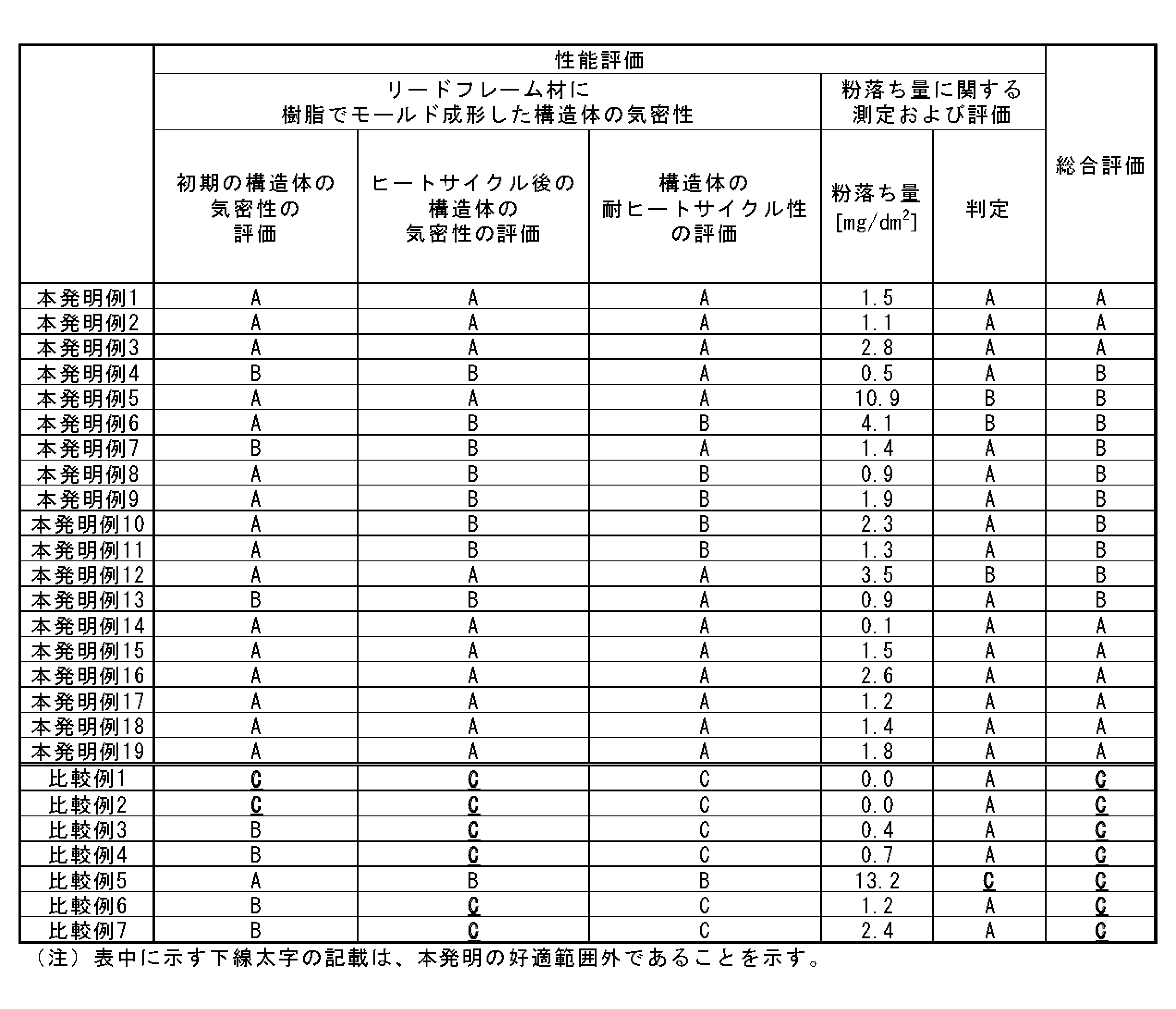
- the leadframe materials 1 of Inventive Examples 1 to 19 had roughened upper surfaces for both the surface coating 3 and the side coating 4, and the ratio h2 / h1 of the average roughness height h2 of the side coating 4 to the average roughness height h1 of the surface coating 3 was within the appropriate range of the present invention.
- the leadframe materials 1 of Inventive Examples 1 to 19 were rated as "A” or "B” in all three evaluation results regarding the initial airtightness of the structure, the airtightness of the structure after the heat cycle test, and the amount of powder falling, and were also rated as "A" or "B” in the overall evaluation.
- Figure 8 shows a secondary electron image of the cross section of the lead frame material of Example 1 of the present invention, observed by SEM. From the secondary electron image in Figure 8, it can be seen that the lead frame material of Example 1 of the present invention has a roughened upper surface for both the surface coating 3 and the side coating 4, and that the average roughness height of the side coating 4 formed on the side 23 of the substrate 2 is clearly greater than the average roughness height of the surface coating 3 formed on the surface 21 of the substrate 2.
- the lead frame materials 1 of invention examples 1 to 19 were all rated "A" or "B" in the overall evaluation, and therefore at least were able to improve the airtightness of the package and were less likely to cause powder falling off, even when subjected to a heat cycle that simulates a harsh usage environment.
- the lead frame materials 1 of Examples 1 to 5, 7, and 12 to 19 of the present invention were rated as "A" in the heat cycle resistance evaluation of the structure when both the first porosity V1 and the second porosity V2 were in the range of 32% or more and 64% or less, and the ratio V2 / V1 of the second porosity V2 to the first porosity V1 was in the range of 0.50 or more and 0.91 or less. Therefore, they were particularly excellent in that they were even less susceptible to a decrease in airtightness due to a heat cycle test.
- the lead frame materials of Comparative Example 1 and Comparative Example 2 did not have either the surface coating 3 or the side coating 4, and the ratio h2 / h1 of the average roughness height h2 of the side coating 4 to the average roughness height h1 of the surface coating 3 in all of Comparative Examples 3 to 7 was outside the appropriate range of the present invention. Therefore, the lead frame materials of Comparative Examples 1 to 7 were rated as "C" in at least one of the three evaluation results regarding the initial airtightness of the structure, the airtightness of the structure after the heat cycle test, and the amount of powder falling, and were also rated as "C" in the overall evaluation.
Landscapes
- Chemical & Material Sciences (AREA)
- Engineering & Computer Science (AREA)
- Chemical Kinetics & Catalysis (AREA)
- Electrochemistry (AREA)
- Materials Engineering (AREA)
- Metallurgy (AREA)
- Organic Chemistry (AREA)
- Lead Frames For Integrated Circuits (AREA)
Abstract
Description
しかしながら、近年要求される半導体パッケージの小型低背化に伴って、パッケージの気密性の合格レベルがより厳しくなることが想定される。
例えば、過酷な使用環境を想定したヒートサイクル、例えば-50℃で30分間保持した後、105℃で30分間保持するサイクルを50回繰り返すヒートサイクル試験を行ったとき、樹脂とリードフレームとの間に隙間が生じるようになり、パッケージの気密性が低下して不良の原因となる場合があることが分かった。これは、従来にはあまり多用されていなかった、より小型なQFN(Quad Flat Non-Leaded Package)タイプおよびSOP(Small Outline Package)タイプなどのパッケージが多く用いられるようになり、モールド樹脂とリードフレーム材の接着面積が減少してきたことに加え、車載用途などで使用環境による温度負荷が増大してきたためと考えられる。特に、リードフレーム材の側面においては、リードフレーム材とモールド樹脂との間での隙間の発生による、パッケージの気密性の低下が顕著になっていた。このように、パッケージの気密性には、未だに改善の余地があることが分かった。
(1)導電性の基体と、前記基体の少なくとも一部の表面および裏面のうちの一方または双方の面に形成される表面被膜と、前記表面被膜に隣接し、前記基体の少なくとも一部の側面に形成される側面被膜と、を有するリードフレーム材であって、前記表面被膜および前記側面被膜は、いずれも粗化された上面を有し、前記表面被膜の平均粗さ高さをh1、前記側面被膜の平均粗さ高さをh2とするとき、前記表面被膜の平均粗さ高さh1に対する前記側面被膜の平均粗さ高さh2の比h2/h1が、1.35以上である、リードフレーム材。
(2)前記表面被膜の平均粗さ高さh1は、0.5μm以上3.5μm以下の範囲であり、かつ、前記側面被膜の平均粗さ高さh2は、1.0μm以上6.5μm以下の範囲である、上記(1)に記載のリードフレーム材。
(3)前記表面被膜の断面で見て、前記表面被膜の上面の最上点の位置を通り、前記基体の表面に対して平行に引いた仮想線l1と、前記表面被膜の上面の最下点の位置を通り、前記基体の表面に対して平行に引いた仮想線n1とで区画される第1測定面積に占める第1空隙率をV1とし、前記側面被膜の断面で見て、前記側面被膜の上面の最上点の位置を通り、前記基体の側面に対して平行に引いた仮想線l2と、前記側面被膜の上面の最下点の位置を通り、前記基体の側面に対して平行に引いた仮想線n2とで区画される第2測定面積に占める第2空隙率をV2とするとき、前記第1空隙率V1に対する前記第2空隙率V2の比V2/V1は、0.50以上0.91以下の範囲である、上記(1)または(2)に記載のリードフレーム材。
(4)前記第1空隙率V1および前記第2空隙率V2は、いずれも32%以上64%以下の範囲である、上記(3)に記載のリードフレーム材。
(5)前記基体は、銅、銅合金、鉄、鉄合金、アルミニウムまたはアルミニウム合金からなる、上記(1)から(4)のいずれか1項に記載のリードフレーム材。
(6)前記基体の厚さをTとするとき、前記側面被膜の平均粗さ高さh2に対する前記基体の厚さTの比(T/h2比)は、15.0以上200.0以下の範囲である、上記(1)から(5)のいずれか1項に記載のリードフレーム材。
(7)前記表面被膜および前記側面被膜は、いずれも粗化層を有する、上記(1)から(6)のいずれか1項に記載のリードフレーム材。
(8)前記粗化層は、銅、銅合金、ニッケルまたはニッケル合金からなる、上記(7)に記載のリードフレーム材。
(9)前記粗化層は、電気めっき層である、上記(7)または(8)に記載のリードフレーム材。
(10)前記表面被膜および前記側面被膜は、前記粗化層の上面に形成される少なくとも1層の表面被覆層をさらに有する、上記(7)から(9)のいずれか1項に記載のリードフレーム材。
(11)前記表面被覆層は、前記粗化層とは異なる組成を有する金属または合金であって、銅、銅合金、ニッケル、ニッケル合金、コバルト、コバルト合金、パラジウム、パラジウム合金、ロジウム、ロジウム合金、ルテニウム、ルテニウム合金、白金、白金合金、イリジウム、イリジウム合金、金、金合金、銀、銀合金、スズ、スズ合金、インジウムまたはインジウム合金からなる、上記(10)に記載のリードフレーム材。
(12)上記(1)から(11)のいずれか1項に記載のリードフレーム材の製造方法であって、電気めっきにより、前記基体に、粗化された上面を有する前記表面被膜および前記側面被膜を形成する被膜形成工程を含む、リードフレーム材の製造方法。
(13)上記(1)から(11)のいずれか1項に記載のリードフレーム材を用いて形成したリードフレームを備える、半導体パッケージ。
図1は、本発明の実施形態に係るリードフレーム材の概略を示す断面図である。本発明のリードフレーム材1は、図1に示すように、リードフレーム材1は、導電性の基体2と、基体2の少なくとも一部の表面21及び裏面22のうちの一方または双方の面に形成される表面被膜3と、表面被膜3に隣接し、基体2の少なくとも一部の側面23に形成される側面被膜4とを有し、表面被膜3および側面被膜4は、いずれも粗化された上面30、40を有する。このリードフレーム材1は、表面被膜3の平均粗さ高さをh1、側面被膜4の平均粗さ高さをh2とするとき、表面被膜3の平均粗さ高さh1に対する側面被膜4の平均粗さ高さh2の比h2/h1が、1.35以上である。
本発明に係るリードフレーム材1は、導電性の基体2と、基体2の少なくとも一部の表面21および裏面22のうちの一方または双方の面に形成される表面被膜3と、表面被膜3に隣接し、基体2の少なくとも一部の側面23に形成される側面被膜4とを有する。
表面被膜3は、基体2の少なくとも一部の表面21及び裏面22のうちの一方または双方の面に形成される被膜である。また、側面被膜4は、表面被膜3に隣接し、基体2の少なくとも一部の側面23に形成される被膜である。そのため、本発明のリードフレーム材1は、上述の導電性の基体2と、表面被膜3と、側面被膜4を有するものである。
図6のリードフレーム材1Aに示すように、表面被膜3Aおよび側面被膜4Aは、粗化層5の上面50に形成される少なくとも1層の表面被覆層6をさらに有することが好ましい。このとき、表面被膜3の平均粗さ高さh1、側面被膜4の平均粗さ高さh2などの測定対象となる表面被膜3Aおよび側面被膜4Aは、粗化層5と、粗化層5の少なくとも表面に形成される表面被覆層6とを有する。このような表面被覆層6を有することで、粗化層5の表面性状によって樹脂との密着性を高めるとともに、リードフレーム材1Aの表面の組成が変わるため、基体2との密着性を向上させながら、はんだとの濡れ性および樹脂との密着性の両方を高めることができる。
上述のリードフレーム材の製造方法は、特に限定されるものではないが、生産性を高めるとともに、表面被膜3の平均粗さ高さh1に対する側面被膜4の平均粗さ高さh2の比h2/h1の制御を行いやすくする観点から、電気めっきにより、基体2に、粗化された上面30、40を有する表面被膜3および側面被膜4を形成する被膜形成工程を含む方法であることが好ましい。その一例として、基体2に電気めっきにより粗化層5を形成する方法であることが好ましい。
めっき浴: 10g/L~35g/L(銅(原子)換算)の硫酸銅
60g/L~180g/Lの硫酸
0.1g/L~5.0g/Lのモリブデン濃度のモリブデン酸アンモニウム
めっき条件:浴温20℃~60℃、電流密度30A/dm2~80A/dm2
リードフレーム材は、半導体素子を支持固定して、ワイヤやプリント基板などによって外部と電気や信号のやり取りを行うための接続端子として用いられ、例えば、リードフレーム材を用いて形成されたリードフレームを備える半導体パッケージに、好ましく用いることができる。ここで、半導体パッケージに実装されうる半導体素子としては、トランジスタやキャパシタ、LEDなどを挙げることができるが、これらに限定されない。
表1に示す種類の金属または合金からなり、予めプレス加工によって縦30mm×横10mmの大きさにした表1に記載される厚さの導電性の基体である基材2を準備し、前処理としてカソード電解脱脂および酸洗を施した。
本発明例1、2、4~17、19および比較例4~7については、電気めっき液として、銅(Cu)金属の濃度として表1に記載される10g/L~50g/Lの範囲の金属濃度である硫酸銅と、60g/L~180g/Lの硫酸と、モリブデン(Mo)金属の濃度として0.1g/L~5.0g/Lの金属濃度であるモリブデン酸アンモニウムとを含む水溶液を調製し、内径80mmの筒状のめっき電解槽に、1Lの電気めっき液を入れた。次いで、本発明例1、2、4~17、19については、基材2の表面21および裏面22の合計のめっき面積に対して表1に記載される割合の面積を遮蔽板によって遮蔽するように、対極との間に遮蔽板を設置した。他方で、比較例4については、基材2の表面21および裏面22の合計のめっき面積に対して40%の面積を遮蔽するように、対極との間に遮蔽板を設置した。また、比較例5~7については、基材2の表面21および裏面22の合計のめっき面積に対して5%の面積を遮蔽するように、対極との間に遮蔽板を設置した。ここに、20℃~60℃の温度で、20A/dm2~80A/dm2の電流密度で通電することで被膜形成工程を行ない、電気めっきにより表面被膜3および側面被膜4を形成させた。
電気めっき液として、ニッケル(Ni)金属の濃度として表1に記載される10g/L~50g/Lの範囲の金属濃度である硫酸ニッケルと、10g/L~30g/Lのホウ酸と、30g/L~100g/Lの塩化ナトリウムと、10mL/L~30mL/Lの25質量%アンモニア水とを含む水溶液を調製した。次いで、内径80mmの筒状のめっき電解槽に、1Lの電気めっき液を入れ、基材2の表面21および裏面22の合計のめっき面積に対して表1に記載される割合の面積を遮蔽板によって遮蔽するように、対極との間に遮蔽板を設置した。ここに、50℃~70℃の温度で、5A/dm2~30A/dm2の電流密度で通電することで被膜形成工程を行ない、電気めっきにより表面被膜3および側面被膜4を形成させた。
電気めっき液として、ニッケル(Ni)金属の濃度として500g/Lの金属濃度であるスルファミン酸ニッケルと、30g/Lの塩化ニッケルと、30g/Lのホウ酸とを含む水溶液を調製した。内径80mmの筒状のめっき電解槽に1Lの電気めっき液を入れて、50℃の温度で、10A/dm2の電流密度で通電することで、電気めっきにより表面被覆層6を形成させた。
電気めっき液として、パラジウム(Pd)金属の濃度として45g/Lの金属濃度であるジクロロテトラアンミンパラジウム(Pd(NH3)4Cl2)と、90mL/Lの25質量%アンモニア水と、50g/Lの硫酸アンモニウムと、10g/LのパラシグマLN光沢剤(商品名、松田産業株式会社製)とを含む水溶液を調製した。内径80mmの筒状のめっき電解槽に1Lの電気めっき液を入れて、60℃の温度で、5A/dm2の電流密度で通電することで、電気めっきにより表面被覆層6を形成させた。
電気めっき液として、金(Au)金属の濃度として14.6g/Lの金属濃度であるシアン化金カリウムと、150g/Lのクエン酸と、180g/Lのクエン酸カリウムとを含む水溶液を調製した。内径80mmの筒状のめっき電解槽に1Lの電気めっき液を入れて、40℃の温度で、1A/dm2の電流密度で通電することで、電気めっきにより表面被覆層6を形成させた。
電気めっき液として、金(Au)金属の濃度として10g/Lの金属濃度であるシアン化金カリウムと、コバルト(Co)金属の濃度として0.1g/Lの金属濃度である炭酸コバルトと、100g/Lのクエン酸と20g/Lのリン酸水素二カリウムとを含む水溶液を調製した。内径80mmの筒状のめっき電解槽に1Lの電気めっき液を入れて、40℃の温度で、1A/dm2の電流密度で通電することで、電気めっきにより表面被覆層6を形成させた。
電気めっき液として、銀(Ag)金属の濃度として93g/Lの金属濃度であるシアン化銀と、132g/Lのシアン化カリウムとを含む水溶液を調製した。内径80mmの筒状のめっき電解槽に1Lの電気めっき液を入れて、20℃の温度で、1A/dm2の電流密度で通電することで、電気めっきにより表面被覆層6を形成させた。
電気めっき液として、錫(Sn)金属の濃度として80g/Lの金属濃度である硫酸錫と、50mL/Lの硫酸と、5mL/LのUTB513Yと、を含む水溶液を調製した。内径80mmの筒状のめっき電解槽に1Lの電気めっき液を入れて、20℃の温度で、5A/dm2の電流密度で通電することで、電気めっきにより表面被覆層6を形成させた。
次に、得られた各層およびリードフレーム材1の特性を、以下のように測定および評価した。なお、得られた各層の特性については、リードフレーム材1の作製中に随時測定した。
表面被膜3の平均粗さ高さh1は、表面被膜3の厚さ方向を含む断面をミクロトーム加工したものについて、走査型電子顕微鏡(SEM)を用いて観察して求めた。ここで、SEMによる観察では、基材2の表面21に形成された表面被膜3と、裏面22に形成された表面被膜3のそれぞれについて、被膜の連続した凹凸10個分を1視野として、それぞれ3視野分のSEM像を無作為に選択し、3視野分のSEM像のそれぞれについて、凹凸の最上点(被膜の上面の最上点)を通る基材2の表面(または裏面)に平行に引いた仮想線と、凹凸の最下点(被膜の上面の最下点)を通る基材2の表面(または裏面)に平行に引いた仮想線とで評価エリアM1を区画し、この評価エリアM1において、表面被膜3が占めている部分(表面被膜3の存在領域P1)の面積を算出した。被膜部分Pの面積の算出は、画像処理ソフトImageJを用いて、下限閾値を128、上限閾値を255にそれぞれ設定し、二値化の設定で、分離点は除く一方で、被膜部分Pの内部を塗りつぶす二値化処理により行なった。このとき得られた被膜部分P1の面積を、線分の長さ(10個の凹凸の幅)L1で割った値を、視野ごとの表面被膜3の平均粗さ高さとして求めた。ここで、基材2の表面21および裏面22の両方に表面被膜3が形成されている例では、表面21側の3視野分および裏面22側の3視野分の合計6視野分の表面被膜3の平均粗さ高さの平均をとって、表面被膜3の平均粗さ高さh1とした。また、基材2の表面21または裏面22の一方に表面被膜3が形成されている例では、表面被膜3が形成されている側の3視野分の表面被膜3の平均粗さ高さの平均をとって、表面被膜3の平均粗さ高さh1とした。結果を表1に示す。
第1空隙率V1は、上述の「[1]表面被膜の平均粗さ高さh1と、側面被膜の平均粗さ高さh2の測定」に用いたSEM像を用い、表面21に形成された表面被膜3と、裏面22に形成された表面被膜3のそれぞれについて、評価エリアM1全体の面積に対する、評価エリアM1の面積から表面被膜3の存在領域P1の面積を引いた空隙部分(表面被膜3の非存在領域S1)の面積の割合を算出することで、視野ごとの空隙率を求めた。すなわち、視野ごとの表面被膜3の空隙率は、以下の(1)式により算出した。
表面被膜3の空隙率(%)=100×{(評価エリアM1の面積)―(表面被膜3の存在領域P1の面積)}/(評価エリアM1の面積) ・・・(1)
これらの視野ごとの空隙率から、基材2の表面21および裏面22の両方に表面被膜3が形成されている例では、表面21側の3視野分および裏面22側の3視野分の合計6視野分の表面被膜3の平均粗さ高さの平均をとって、第1空隙率V1(%)とした。また、基材2の表面21または裏面22の一方に表面被膜3が形成されている例では、表面被膜3が形成されている側の3視野分の表面被膜3の空隙率の平均をとって、第1空隙率V1とした。
側面被膜4の空隙率(%)=100×{(評価エリアM2の面積)―(側面被膜4の存在領域P2の面積)}/(評価エリアM2の面積) ・・・(2)
これらの視野ごとの空隙率から、3視野分の側面被膜4の空隙率の平均をとって、第2空隙率V2(%)とした。
表面被覆層6の厚さは、JIS H8501:1999に準拠した蛍光X線式試験方法によって測定した。具体的には、蛍光X線膜厚計(SFT9400、エスアイアイ・ナノテクノロジー社製)を用い、コリメータ径0.5mmとして、各層の任意の10箇所を測定し、これらの測定値の平均値を算出することで、表面被覆層6の厚さを得た。結果を表1に示す。
図7に、本発明例のリードフレーム材について行う樹脂との密着性の測定における、リードフレーム材1と樹脂との位置関係を示す模式図を示す。本発明例および比較例で得られたリードフレーム材1について、図7に示されるように、リードフレーム材1を覆うように樹脂7でモールド成形した構造体について、グロスリーク試験を行なった。ここで、グロスリーク試験は、120℃±10℃に加熱した高沸点溶剤であるフロリナートFC-40(登録商標)に上記構造体を30秒間または120秒間浸漬し、浸漬中に気泡が発生するか否かによって、リードフレーム材1からの空気の漏れの有無を判定し、その判定結果からリードフレーム材1の気密性を評価した。
本発明例および比較例で得られたリードフレーム材1について、リードフレーム材を60mm幅に切り出して、JIS H 8504に規定されるテープ剥離試験を行ない、試験の前後における質量の減少量を脱離量(粉落ち量)として測定および評価した。測定された脱離量について、3mg/dm2未満で合った場合を粉落ちが起こり難い点で特に優れているとして「A」と評価した。また、脱離量が3mg/dm2以上12mg/dm2未満の範囲であった場合を、粉落ちが起こり難い点で優れているとして「B」と評価した。他方で、脱離量が12mg/dm2以上であった場合を、粉落ちが起こり易い点で望ましくないとして「C」と評価した。結果を表2に示す。
これらの評価結果のうち、初期の構造体の気密性と、ヒートサイクル試験後の構造体の気密性と、粉落ち量に関する3つの評価結果について、3つとも「A」と評価した場合を、ヒートサイクル試験の前後のいずれにおいても気密性が高く、かつ粉落ちが起こり難い点で特に優れているとして「A」と評価した。また、これら3つの評価結果について、3つとも「A」または「B」と評価した場合(ただし、3つとも「A」と評価した場合を除く)を、ヒートサイクル試験の前後のいずれにおいても気密性が高く、かつ粉落ちが起こり難い点で優れているとして「B」と評価した。他方で、これら3つの評価結果について、少なくともいずれかで評価結果が「C」になった場合を、ヒートサイクル試験の前後のうち少なくともいずれかにおける気密性が不合格であり、または粉落ちが起こりやすい点で不合格であるとして「C」と評価した。結果を表2に示す。
さらに、初期の構造体の気密性の評価結果と、ヒートサイクル試験後の構造体の気密性の評価結果について、初期の気密性を「A」または「B」と評価し、かつヒートサイクル試験後の気密性を「A」と評価した場合と、初期の気密性を「B」と評価し、かつヒートサイクル試験後の気密性を「B」と評価した場合を、構造体が耐ヒートサイクル性に特に優れているとして「A」と評価した。また、初期の気密性を「A」と評価し、かつヒートサイクル試験後の気密性を「B」と評価した場合を、構造体が耐ヒートサイクル性に優れているとして「B」と評価した。他方で、初期とヒートサイクル試験後の気密性のうち、少なくともいずれかの評価結果を「C」と評価した場合を、耐ヒートサイクル性が低い点で望ましくないとして「C」と評価した。結果を表2に示す。

2 基体(または基材)
21 基体の表面
22 基体の裏面
23 基体の側面
3、3A 表面被膜
30 表面被膜の上面
4 側面被膜
40 側面被膜の上面
5 粗化層
50 粗化層の上面
6 表面被覆層
7 樹脂
h1 表面被膜の平均粗さ高さ
h2 側面被膜の平均粗さ高さ
A1 表面被膜の上面の最上点
B1 表面被膜の上面の最下点
P1 評価エリアに占める表面被膜の存在領域
S1 評価エリアに占める表面被膜の非存在領域
A2 側面被膜の上面の最上点
B2 側面被膜の上面の最下点
P2 評価エリアに占める側面被膜の存在領域
S2 評価エリアに占める側面被膜の非存在領域
L1、L2 線分の長さ(10個の凹凸の幅)
M1、M2 評価エリア
Claims (13)
- 導電性の基体と、
前記基体の少なくとも一部の表面および裏面のうちの一方または双方の面に形成される表面被膜と、
前記表面被膜に隣接し、前記基体の少なくとも一部の側面に形成される側面被膜と、
を有するリードフレーム材であって、
前記表面被膜および前記側面被膜は、いずれも粗化された上面を有し、
前記表面被膜の平均粗さ高さをh1、前記側面被膜の平均粗さ高さをh2とするとき、
前記表面被膜の平均粗さ高さh1に対する前記側面被膜の平均粗さ高さh2の比h2/h1が、1.35以上である、リードフレーム材。 - 前記表面被膜の平均粗さ高さh1は、0.5μm以上3.5μm以下の範囲であり、かつ、
前記側面被膜の平均粗さ高さh2は、1.0μm以上6.5μm以下の範囲である、請求項1に記載のリードフレーム材。 - 前記表面被膜の断面で見て、前記表面被膜の上面の最上点の位置を通り、前記基体の表面に対して平行に引いた仮想線l1と、前記表面被膜の上面の最下点の位置を通り、前記基体の表面に対して平行に引いた仮想線n1とで区画される第1測定面積に占める第1空隙率をV1とし、
前記側面被膜の断面で見て、前記側面被膜の上面の最上点の位置を通り、前記基体の側面に対して平行に引いた仮想線l2と、前記側面被膜の上面の最下点の位置を通り、前記基体の側面に対して平行に引いた仮想線n2とで区画される第2測定面積に占める第2空隙率をV2とするとき、
前記第1空隙率V1に対する前記第2空隙率V2の比V2/V1は、0.50以上0.91以下の範囲である、請求項1に記載のリードフレーム材。 - 前記第1空隙率V1および前記第2空隙率V2は、いずれも32%以上64%以下の範囲である、請求項3に記載のリードフレーム材。
- 前記基体は、銅、銅合金、鉄、鉄合金、アルミニウムまたはアルミニウム合金からなる、請求項1に記載のリードフレーム材。
- 前記基体の厚さをTとするとき、前記側面被膜の平均粗さ高さh2に対する前記基体の厚さTの比(T/h2比)は、15.0以上200.0以下の範囲である、請求項1に記載のリードフレーム材。
- 前記表面被膜および前記側面被膜は、いずれも粗化層を有する、請求項1に記載のリードフレーム材。
- 前記粗化層は、銅、銅合金、ニッケルまたはニッケル合金からなる、請求項7に記載のリードフレーム材。
- 前記粗化層は、電気めっき層である、請求項7に記載のリードフレーム材。
- 前記表面被膜および前記側面被膜は、前記粗化層の上面に形成される少なくとも1層の表面被覆層をさらに有する、請求項7に記載のリードフレーム材。
- 前記表面被覆層は、前記粗化層とは異なる組成を有する金属または合金であって、銅、銅合金、ニッケル、ニッケル合金、コバルト、コバルト合金、パラジウム、パラジウム合金、ロジウム、ロジウム合金、ルテニウム、ルテニウム合金、白金、白金合金、イリジウム、イリジウム合金、金、金合金、銀、銀合金、スズ、スズ合金、インジウムまたはインジウム合金からなる、請求項10に記載のリードフレーム材。
- 請求項1から11のいずれか1項に記載のリードフレーム材の製造方法であって、
電気めっきにより、前記基体に、粗化された上面を有する前記表面被膜および前記側面被膜を形成する被膜形成工程を含む、リードフレーム材の製造方法。 - 請求項1から11のいずれか1項に記載のリードフレーム材を用いて形成したリードフレームを備える、半導体パッケージ。
Priority Applications (3)
| Application Number | Priority Date | Filing Date | Title |
|---|---|---|---|
| KR1020257031191A KR20260025290A (ko) | 2023-06-16 | 2024-06-12 | 리드 프레임재와 그 제조 방법 및 반도체 패키지 |
| CN202480021561.1A CN120917185A (zh) | 2023-06-16 | 2024-06-12 | 导线架材料及其制造方法、以及半导体封装体 |
| JP2025527965A JPWO2024257796A1 (ja) | 2023-06-16 | 2024-06-12 |
Applications Claiming Priority (2)
| Application Number | Priority Date | Filing Date | Title |
|---|---|---|---|
| JP2023-098902 | 2023-06-16 | ||
| JP2023098902 | 2023-06-16 |
Publications (1)
| Publication Number | Publication Date |
|---|---|
| WO2024257796A1 true WO2024257796A1 (ja) | 2024-12-19 |
Family
ID=93852158
Family Applications (1)
| Application Number | Title | Priority Date | Filing Date |
|---|---|---|---|
| PCT/JP2024/021338 Ceased WO2024257796A1 (ja) | 2023-06-16 | 2024-06-12 | リードフレーム材およびその製造方法、ならびに半導体パッケージ |
Country Status (5)
| Country | Link |
|---|---|
| JP (1) | JPWO2024257796A1 (ja) |
| KR (1) | KR20260025290A (ja) |
| CN (1) | CN120917185A (ja) |
| TW (1) | TW202501763A (ja) |
| WO (1) | WO2024257796A1 (ja) |
Citations (4)
| Publication number | Priority date | Publication date | Assignee | Title |
|---|---|---|---|---|
| WO2015188971A1 (de) * | 2014-06-13 | 2015-12-17 | Robert Bosch Gmbh | Substrat mit einer oberflächenbeschichtung und verfahren zum beschichten einer oberfläche eines substrates |
| JP2017098291A (ja) * | 2015-11-18 | 2017-06-01 | 株式会社三井ハイテック | リードフレーム及びリードフレームパッケージ、並びにこれらの製造方法 |
| JP2020167207A (ja) * | 2019-03-28 | 2020-10-08 | 大口マテリアル株式会社 | 半導体素子搭載用部品、リードフレーム及び半導体素子搭載用基板 |
| WO2023033126A1 (ja) * | 2021-09-03 | 2023-03-09 | 大日本印刷株式会社 | リードフレーム及びその製造方法 |
-
2024
- 2024-06-12 WO PCT/JP2024/021338 patent/WO2024257796A1/ja not_active Ceased
- 2024-06-12 KR KR1020257031191A patent/KR20260025290A/ko active Pending
- 2024-06-12 CN CN202480021561.1A patent/CN120917185A/zh active Pending
- 2024-06-12 JP JP2025527965A patent/JPWO2024257796A1/ja active Pending
- 2024-06-14 TW TW113122037A patent/TW202501763A/zh unknown
Patent Citations (4)
| Publication number | Priority date | Publication date | Assignee | Title |
|---|---|---|---|---|
| WO2015188971A1 (de) * | 2014-06-13 | 2015-12-17 | Robert Bosch Gmbh | Substrat mit einer oberflächenbeschichtung und verfahren zum beschichten einer oberfläche eines substrates |
| JP2017098291A (ja) * | 2015-11-18 | 2017-06-01 | 株式会社三井ハイテック | リードフレーム及びリードフレームパッケージ、並びにこれらの製造方法 |
| JP2020167207A (ja) * | 2019-03-28 | 2020-10-08 | 大口マテリアル株式会社 | 半導体素子搭載用部品、リードフレーム及び半導体素子搭載用基板 |
| WO2023033126A1 (ja) * | 2021-09-03 | 2023-03-09 | 大日本印刷株式会社 | リードフレーム及びその製造方法 |
Also Published As
| Publication number | Publication date |
|---|---|
| TW202501763A (zh) | 2025-01-01 |
| KR20260025290A (ko) | 2026-02-24 |
| JPWO2024257796A1 (ja) | 2024-12-19 |
| CN120917185A (zh) | 2025-11-07 |
Similar Documents
| Publication | Publication Date | Title |
|---|---|---|
| CN108026657B (zh) | 引线框材料及其制造方法 | |
| JP6685112B2 (ja) | リードフレーム及びリードフレームパッケージ、並びにこれらの製造方法 | |
| TWI751150B (zh) | 引線框架材及其製造方法 | |
| JP4639701B2 (ja) | 錫めっき皮膜を有する金属板及びそれを備えた電子部品並びに錫めっき皮膜の製造方法 | |
| CN101595248A (zh) | Sn-B电镀液以及使用该电镀液的电镀方法 | |
| JP7178530B1 (ja) | リードフレーム材およびその製造方法、ならびに半導体パッケージ | |
| JP2020063493A (ja) | 導電性材料、成型品及び電子部品 | |
| JP7366480B1 (ja) | リードフレーム材およびその製造方法、ならびにリードフレーム材を用いた半導体パッケージ | |
| JP2020063492A (ja) | 導電性材料、成型品及び電子部品 | |
| TWI788542B (zh) | 引線框架材料及其製造方法、以及使用此引線框架材料之半導體封裝體 | |
| KR102918295B1 (ko) | 리드 프레임재와 그 제조 방법 및 반도체 패키지 | |
| KR20260025290A (ko) | 리드 프레임재와 그 제조 방법 및 반도체 패키지 | |
| JP2022148743A (ja) | 導電性材料、成型品及び電子部品 | |
| JP7809883B1 (ja) | 電子部品用材料およびその製造方法、リードフレーム材およびその製造方法、ならびに半導体パッケージ | |
| JP6827150B1 (ja) | リードフレーム材およびその製造方法ならびにリードフレームおよび電気電子部品 | |
| JP2024143836A (ja) | リードフレーム、導電部品及び複合体 | |
| JP2026023021A (ja) | 電子部品用材料およびその製造方法、リードフレーム材およびその製造方法、ならびに半導体パッケージ | |
| JP2026023020A (ja) | 電子部品用材料およびその製造方法、リードフレーム材およびその製造方法、ならびに半導体パッケージ | |
| JP2024101669A (ja) | 金属部品 |
Legal Events
| Date | Code | Title | Description |
|---|---|---|---|
| 121 | Ep: the epo has been informed by wipo that ep was designated in this application |
Ref document number: 24823411 Country of ref document: EP Kind code of ref document: A1 |
|
| WWE | Wipo information: entry into national phase |
Ref document number: 2025527965 Country of ref document: JP |
|
| WWE | Wipo information: entry into national phase |
Ref document number: 202480021561.1 Country of ref document: CN |
|
| WWP | Wipo information: published in national office |
Ref document number: 202480021561.1 Country of ref document: CN |
|
| NENP | Non-entry into the national phase |
Ref country code: DE |
|
| 122 | Ep: pct application non-entry in european phase |
Ref document number: 24823411 Country of ref document: EP Kind code of ref document: A1 |