WO2024257659A1 - 半導体発光素子 - Google Patents
半導体発光素子 Download PDFInfo
- Publication number
- WO2024257659A1 WO2024257659A1 PCT/JP2024/020448 JP2024020448W WO2024257659A1 WO 2024257659 A1 WO2024257659 A1 WO 2024257659A1 JP 2024020448 W JP2024020448 W JP 2024020448W WO 2024257659 A1 WO2024257659 A1 WO 2024257659A1
- Authority
- WO
- WIPO (PCT)
- Prior art keywords
- protective film
- semiconductor light
- protective
- film
- emitting element
- Prior art date
- Legal status (The legal status is an assumption and is not a legal conclusion. Google has not performed a legal analysis and makes no representation as to the accuracy of the status listed.)
- Ceased
Links
Images









Classifications
-
- H—ELECTRICITY
- H01—ELECTRIC ELEMENTS
- H01S—DEVICES USING THE PROCESS OF LIGHT AMPLIFICATION BY STIMULATED EMISSION OF RADIATION [LASER] TO AMPLIFY OR GENERATE LIGHT; DEVICES USING STIMULATED EMISSION OF ELECTROMAGNETIC RADIATION IN WAVE RANGES OTHER THAN OPTICAL
- H01S5/00—Semiconductor lasers
- H01S5/02—Structural details or components not essential to laser action
- H01S5/028—Coatings ; Treatment of the laser facets, e.g. etching, passivation layers or reflecting layers
- H01S5/0282—Passivation layers or treatments
-
- H—ELECTRICITY
- H01—ELECTRIC ELEMENTS
- H01S—DEVICES USING THE PROCESS OF LIGHT AMPLIFICATION BY STIMULATED EMISSION OF RADIATION [LASER] TO AMPLIFY OR GENERATE LIGHT; DEVICES USING STIMULATED EMISSION OF ELECTROMAGNETIC RADIATION IN WAVE RANGES OTHER THAN OPTICAL
- H01S5/00—Semiconductor lasers
- H01S5/0014—Measuring characteristics or properties thereof
- H01S5/0021—Degradation or life time measurements
-
- H—ELECTRICITY
- H01—ELECTRIC ELEMENTS
- H01S—DEVICES USING THE PROCESS OF LIGHT AMPLIFICATION BY STIMULATED EMISSION OF RADIATION [LASER] TO AMPLIFY OR GENERATE LIGHT; DEVICES USING STIMULATED EMISSION OF ELECTROMAGNETIC RADIATION IN WAVE RANGES OTHER THAN OPTICAL
- H01S5/00—Semiconductor lasers
- H01S5/02—Structural details or components not essential to laser action
- H01S5/028—Coatings ; Treatment of the laser facets, e.g. etching, passivation layers or reflecting layers
-
- H—ELECTRICITY
- H01—ELECTRIC ELEMENTS
- H01S—DEVICES USING THE PROCESS OF LIGHT AMPLIFICATION BY STIMULATED EMISSION OF RADIATION [LASER] TO AMPLIFY OR GENERATE LIGHT; DEVICES USING STIMULATED EMISSION OF ELECTROMAGNETIC RADIATION IN WAVE RANGES OTHER THAN OPTICAL
- H01S5/00—Semiconductor lasers
- H01S5/02—Structural details or components not essential to laser action
- H01S5/028—Coatings ; Treatment of the laser facets, e.g. etching, passivation layers or reflecting layers
- H01S5/0281—Coatings made of semiconductor materials
-
- H—ELECTRICITY
- H01—ELECTRIC ELEMENTS
- H01S—DEVICES USING THE PROCESS OF LIGHT AMPLIFICATION BY STIMULATED EMISSION OF RADIATION [LASER] TO AMPLIFY OR GENERATE LIGHT; DEVICES USING STIMULATED EMISSION OF ELECTROMAGNETIC RADIATION IN WAVE RANGES OTHER THAN OPTICAL
- H01S5/00—Semiconductor lasers
- H01S5/02—Structural details or components not essential to laser action
- H01S5/028—Coatings ; Treatment of the laser facets, e.g. etching, passivation layers or reflecting layers
- H01S5/0282—Passivation layers or treatments
- H01S5/0283—Optically inactive coating on the facet, e.g. half-wave coating
-
- H—ELECTRICITY
- H01—ELECTRIC ELEMENTS
- H01S—DEVICES USING THE PROCESS OF LIGHT AMPLIFICATION BY STIMULATED EMISSION OF RADIATION [LASER] TO AMPLIFY OR GENERATE LIGHT; DEVICES USING STIMULATED EMISSION OF ELECTROMAGNETIC RADIATION IN WAVE RANGES OTHER THAN OPTICAL
- H01S5/00—Semiconductor lasers
- H01S5/02—Structural details or components not essential to laser action
- H01S5/028—Coatings ; Treatment of the laser facets, e.g. etching, passivation layers or reflecting layers
- H01S5/0287—Facet reflectivity
-
- H—ELECTRICITY
- H01—ELECTRIC ELEMENTS
- H01S—DEVICES USING THE PROCESS OF LIGHT AMPLIFICATION BY STIMULATED EMISSION OF RADIATION [LASER] TO AMPLIFY OR GENERATE LIGHT; DEVICES USING STIMULATED EMISSION OF ELECTROMAGNETIC RADIATION IN WAVE RANGES OTHER THAN OPTICAL
- H01S5/00—Semiconductor lasers
- H01S5/20—Structure or shape of the semiconductor body to guide the optical wave ; Confining structures perpendicular to the optical axis, e.g. index or gain guiding, stripe geometry, broad area lasers, gain tailoring, transverse or lateral reflectors, special cladding structures, MQW barrier reflection layers
- H01S5/22—Structure or shape of the semiconductor body to guide the optical wave ; Confining structures perpendicular to the optical axis, e.g. index or gain guiding, stripe geometry, broad area lasers, gain tailoring, transverse or lateral reflectors, special cladding structures, MQW barrier reflection layers having a ridge or stripe structure
-
- H—ELECTRICITY
- H01—ELECTRIC ELEMENTS
- H01S—DEVICES USING THE PROCESS OF LIGHT AMPLIFICATION BY STIMULATED EMISSION OF RADIATION [LASER] TO AMPLIFY OR GENERATE LIGHT; DEVICES USING STIMULATED EMISSION OF ELECTROMAGNETIC RADIATION IN WAVE RANGES OTHER THAN OPTICAL
- H01S5/00—Semiconductor lasers
- H01S5/30—Structure or shape of the active region; Materials used for the active region
- H01S5/34—Structure or shape of the active region; Materials used for the active region comprising quantum well or superlattice structures, e.g. single quantum well [SQW] lasers, multiple quantum well [MQW] lasers or graded index separate confinement heterostructure [GRINSCH] lasers
- H01S5/343—Structure or shape of the active region; Materials used for the active region comprising quantum well or superlattice structures, e.g. single quantum well [SQW] lasers, multiple quantum well [MQW] lasers or graded index separate confinement heterostructure [GRINSCH] lasers in AIIIBV compounds, e.g. AlGaAs-laser, InP-based laser
-
- H—ELECTRICITY
- H01—ELECTRIC ELEMENTS
- H01S—DEVICES USING THE PROCESS OF LIGHT AMPLIFICATION BY STIMULATED EMISSION OF RADIATION [LASER] TO AMPLIFY OR GENERATE LIGHT; DEVICES USING STIMULATED EMISSION OF ELECTROMAGNETIC RADIATION IN WAVE RANGES OTHER THAN OPTICAL
- H01S5/00—Semiconductor lasers
- H01S5/30—Structure or shape of the active region; Materials used for the active region
- H01S5/34—Structure or shape of the active region; Materials used for the active region comprising quantum well or superlattice structures, e.g. single quantum well [SQW] lasers, multiple quantum well [MQW] lasers or graded index separate confinement heterostructure [GRINSCH] lasers
- H01S5/343—Structure or shape of the active region; Materials used for the active region comprising quantum well or superlattice structures, e.g. single quantum well [SQW] lasers, multiple quantum well [MQW] lasers or graded index separate confinement heterostructure [GRINSCH] lasers in AIIIBV compounds, e.g. AlGaAs-laser, InP-based laser
- H01S5/34333—Structure or shape of the active region; Materials used for the active region comprising quantum well or superlattice structures, e.g. single quantum well [SQW] lasers, multiple quantum well [MQW] lasers or graded index separate confinement heterostructure [GRINSCH] lasers in AIIIBV compounds, e.g. AlGaAs-laser, InP-based laser with a well layer based on Ga(In)N or Ga(In)P, e.g. blue laser
-
- H—ELECTRICITY
- H01—ELECTRIC ELEMENTS
- H01S—DEVICES USING THE PROCESS OF LIGHT AMPLIFICATION BY STIMULATED EMISSION OF RADIATION [LASER] TO AMPLIFY OR GENERATE LIGHT; DEVICES USING STIMULATED EMISSION OF ELECTROMAGNETIC RADIATION IN WAVE RANGES OTHER THAN OPTICAL
- H01S2301/00—Functional characteristics
- H01S2301/17—Semiconductor lasers comprising special layers
- H01S2301/176—Specific passivation layers on surfaces other than the emission facet
Definitions
- This disclosure relates to semiconductor light-emitting devices.
- COD catastrophic optical damage
- the semiconductor laser element described in Patent Document 1 aims to improve adhesion of the protective film to the end face by reducing the stress applied to the active layer.
- a protective film made of an aluminum oxide film is placed on the end face that constitutes the resonator.
- the first reaction is a reaction in which oxygen is diffused from the outside to the inside of the protective film, thereby oxidizing the end face.
- the second reaction is a reaction in which the protective film gradually undergoes photocrystallization, causing the protective film to expand or contract.
- the semiconductor laser element described in Patent Document 1 does not have sufficient reliability for high optical output operation.
- the present disclosure aims to solve these problems and provide a highly reliable semiconductor light-emitting device.
- one aspect of the semiconductor light-emitting device disclosed herein has a first end face and a second end face that face each other and form a resonator, and includes a laminated structure including a nitride semiconductor and a protective film disposed on the first end face, the protective film including a first protective film that is an aluminum oxide film or an oxynitride film to which scandium has been added.
- This disclosure makes it possible to provide a highly reliable semiconductor light-emitting element.
- FIG. 1 is a schematic cross-sectional view showing a configuration of a semiconductor light emitting device according to a first embodiment.
- 2 is a cross-sectional view showing a configuration of a protective film according to the first embodiment.
- FIG. 11 is a graph showing an overview of the relationship between the photo-crystallization amount and the oxygen diffusion amount of the first protective film in accordance with the first embodiment and the fifth protective film in accordance with the first comparative example, and the relationship between the driving time and the photo-crystallization amount and the oxygen diffusion amount of the first protective film in accordance with the first comparative example.
- 1 is a transmission electron microscope image of the protective film of Comparative Example 1.
- 4 is a first transmission electron microscope image of the protective film according to the first embodiment.
- FIG. 11 is a second transmission electron microscope image of the protective film according to the first embodiment.
- 11 is a schematic diagram showing photocrystallization and oxygen diffusion in the fifth protective film of Comparative Example 1.
- FIG. 5A to 5C are schematic diagrams showing photocrystallization and oxygen diffusion in a first protective film according to the first embodiment.
- 1 is a graph showing the relationship between the optical output degradation rate and the aging time of each of the semiconductor light-emitting elements of the first embodiment and the first to third comparative examples.
- 1 is a graph showing the relationship between the rate of change in laser oscillation threshold current (Ith) and aging time for each of the semiconductor light-emitting elements of the first embodiment and the first to third comparative examples.
- Ith laser oscillation threshold current
- FIG. 1 is a graph showing the relationship between the rate of change in slope efficiency (Se) and the aging time for each of the semiconductor light emitting devices of the first embodiment and the first to third comparative examples.
- 1 is a schematic diagram showing the shape of the surface of a fifth protective film of Comparative Example 1.
- FIG. 3 is a schematic diagram showing the shape of the surface of a first protective film according to the first embodiment;
- FIG. 11 is a cross-sectional view showing a configuration of a protective film according to a second embodiment.
- FIG. 11 is a cross-sectional view showing a configuration of a protective film according to a third embodiment.
- FIG. 11 is a cross-sectional view showing a configuration of a protective film according to a fourth embodiment.
- FIG. 13 is a cross-sectional view showing a configuration of a protective film according to a fifth embodiment.
- FIG. 13 is a cross-sectional view showing a configuration of a protective film according to a sixth embodiment.
- FIG. 13 is a cross-sectional view showing a configuration of a protective film according to a seventh embodiment.
- FIG. 13 is a cross-sectional view showing a configuration of a protective film according to an eighth embodiment.
- each figure is a schematic diagram and is not necessarily an exact illustration. Therefore, the scale and the like are not necessarily the same in each figure.
- the same reference numerals are used in each figure for substantially the same configuration, and duplicate explanations are omitted or simplified.
- the terms “above” and “below” do not refer to vertically above and below in an absolute spatial sense, but are used as terms defined by a relative positional relationship based on the stacking order in a stacked configuration. Furthermore, the terms “above” and “below” are applied not only to cases where two components are arranged with a gap between them and another component exists between the two components, but also to cases where two components are arranged in contact with each other.
- Fig. 1 is a schematic cross-sectional view showing the configuration of a semiconductor light emitting device 1 according to the present embodiment.
- Fig. 1 shows a cross section parallel to the resonance direction of light of the semiconductor light emitting device 1 and the stacking direction of the stacked structure 2.
- the semiconductor light-emitting element 1 is a semiconductor element that emits light.
- the semiconductor light-emitting element 1 is an edge-emitting nitride-based semiconductor laser element that includes a nitride semiconductor and emits laser light in the ultraviolet range.
- the semiconductor light-emitting element 1 according to this embodiment includes a stacked structure 2 and protective films 3 and 4.
- the laminated structure 2 has a first end face 2F and a second end face 2R that face each other and form a resonator, and includes a nitride semiconductor.
- the first end face 2F and the second end face 2R are faces located at the ends of the resonance direction (horizontal direction in FIG. 1) of the light emitted by the semiconductor light-emitting element 1.
- the resonance direction is a direction perpendicular to the stacking direction (vertical direction in FIG. 1) of each layer included in the laminated structure 2.
- the first end face 2F is a front end face from which light from the semiconductor light-emitting element 1 is emitted.
- a protective film 3 is disposed on the first end face 2F.
- the second end face 2R is a rear end face that reflects light from the semiconductor light-emitting element 1.
- a protective film 4 is disposed on the second end face 2R.
- the laminated structure 2 has a substrate 21, a first semiconductor layer 22, an active layer 23, and a second semiconductor layer 24.
- the substrate 21 is a plate-like member that serves as the base of the laminated structure 2.
- the substrate 21 is an n-type GaN substrate with a (0001) plane.
- the first end face 2F and the second end face 2R are M-planes.
- the first semiconductor layer 22 is disposed above the substrate 21 and includes a semiconductor layer of a first conductivity type.
- the first conductivity type is n-type
- the first semiconductor layer 22 includes an n-side cladding layer made of an n-type nitride semiconductor.
- the first semiconductor layer 22 may include an n-type or undoped semiconductor layer other than the n-side cladding layer.
- the active layer 23 is disposed above the first semiconductor layer 22 and is a layer that emits light.
- the active layer 23 is a quantum well active layer that includes multiple barrier layers and one or more well layers.
- the active layer 23 may also include a first optical guide layer that has a higher average refractive index than the first semiconductor layer 22, a second optical guide layer that has a higher average refractive index than the second semiconductor layer 24, and the like.
- the second semiconductor layer 24 is disposed above the active layer 23 and includes a semiconductor layer of a second conductivity type.
- the second conductivity type is a conductivity type different from the first conductivity type.
- the second conductivity type is p-type
- the second semiconductor layer 24 includes a p-side cladding layer made of a p-type nitride semiconductor.
- the second semiconductor layer 24 may include a p-type or undoped semiconductor layer other than the p-side cladding layer.
- electrodes may be arranged on the laminated structure 2. That is, electrodes may be arranged on the lower surface of the substrate 21 (i.e., of the two main surfaces of the substrate 21, the main surface on the back side of the main surface on which the first semiconductor layer 22 is laminated) and the upper surface of the second semiconductor layer 24 (i.e., of the two main surfaces of the second semiconductor layer 24, the main surface on the back side of the main surface in contact with the active layer 23).
- FIG. 2 is a cross-sectional view showing the configuration of the protective film 3 according to this embodiment.
- FIG. 2 also shows the laminated structure 2.
- FIG. 2 shows a cross section parallel to the resonance direction of light in the semiconductor light-emitting element 1 and the laminated direction of the laminated structure 2.
- the protective film 3 includes at least one of a first protective film and a second protective film. As shown in FIG. 2, the protective film 3 includes first protective films 31a and 31b. The protective film 3 also includes second protective films 32a and 32b. In this embodiment, the protective film 3 further includes a third protective film 33 and a fourth protective film 34. As shown in FIG. 2, each layer included in the protective film 3 is stacked on the first end surface 2F.
- Each of the first protective films 31a and 31b is an oxide film or an oxynitride film of aluminum (Al) to which scandium (Sc) is added.
- each of the first protective films 31a and 31b is an Al 2 O 3 (Al 2 O 3 :Sc) film to which scandium is added.
- the concentration of scandium added to the first protective films 31a and 31b is greater than 0 atomic % (hereinafter, referred to as at%) and is 10 at% or less.
- the concentration of scandium added to the first protective films 31a and 31b may be 7 at% or less, 5 at% or less, 3 at% or less, or 1 at% or less.
- the film thickness of the first protective film 31a is 12 nm, and the film thickness of the first protective film 31b is 152 nm.
- Each of the first protective films 31a and 31b is amorphous or amorphous containing a crystalline phase, but may be crystalline.
- the second protective film 32a is disposed between the first end face 2F and the first protective film 31a.
- the second protective film 32b is disposed between the first end face 2F and the first protective film 31b.
- the second protective film 32a contacts the first protective film 31a, and the second protective film 32b contacts the first protective film 31b.
- the protective film 3 includes a plurality of laminated films 38a, 38b, and each of the plurality of laminated films 38a, 38b includes a first protective film and a second protective film in contact with the first protective film.
- the laminated film 38a includes the first protective film 31a and the second protective film 32a in contact with the first protective film 31a
- the laminated film 38b includes the first protective film 31b and the second protective film 32b in contact with the first protective film 31b.
- the protective film 3 includes two laminated films 38a and 38b, but it may include a single laminated film or three or more laminated films.
- Each of the second protective films 32a, 32b is a crystalline film made of aluminum nitride or oxynitride.
- the second protective films 32a, 32b are AlON (AlON:Sc) films doped with scandium.
- the concentration of scandium added to the second protective films 32a, 32b is greater than 0 at% and is equal to or less than 10 at%.
- the concentration of scandium added to the second protective films 32a, 32b may be equal to or less than 7 at%, equal to or less than 5 at%, equal to or less than 3 at%, or equal to or less than 1 at%.
- the concentration of scandium added to the second protective films 32a, 32b may be equal to or more than 0.1 at%.
- the concentration of scandium added to the second protective films 32a, 32b is 0.3 at%.
- the composition ratio of the second protective film 32a may be different from that of the second protective film 32b.
- the thickness of the second protective film 32a is 20 nm, and the thickness of the second protective film 32b is 10 nm.
- the crystal structure of the second protective films 32a and 32b is a polycrystalline structure consisting of at least one of a hexagonal crystal and a cubic crystal.
- the cubic crystal means a cubic crystal in the narrow sense that does not include a crystal of a perovskite structure.
- the second protective films 32a and 32b are hexagonal crystals with an m-axis orientation with respect to the first end face 2F.
- the second protective films 32a and 32b are hexagonal crystals with an m-axis orientation, but the orientation characteristics of the second protective films 32a and 32b are not limited thereto.
- the orientation characteristics of the second protective films 32a and 32b may be c-axis orientation, mc mixed orientation (i.e., an orientation characteristic in which m-axis orientation and c-axis orientation are mixed), or oblique orientation.
- the third protective film 33 contacts the first end face 2F.
- the third protective film 33 is disposed between the first end face 2F and the second protective film 32a.
- the third protective film 33 is a silicon nitride film or an oxynitride film.
- the third protective film 33 is a SiN film having a thickness of 0.5 nm.
- the third protective film 33 is amorphous.
- the fourth protective film 34 is a silicon oxide film.
- the fourth protective film 34 is disposed at a position farther from the first end face 2F than the first protective films 31a and 31b.
- the first protective films 31a and 31b are disposed between the first end face 2F and the fourth protective film 34.
- the first protective film 31b contacts the fourth protective film 34.
- the fourth protective film 34 is a SiO2 film having a thickness of 54 nm.
- the fourth protective film 34 is amorphous.
- the protective film 4 is disposed on the second end face 2R.
- the protective film 4 may include a first protective film that is an aluminum oxide film or oxynitride film with scandium added, similar to the protective film 3.
- the protective film 4 may also include a protective film having a composition similar to at least one of the second protective films 32a, 32b, the third protective film 33, and the fourth protective film 34.
- the reflectance at the second end face 2R on which the protective film 4 is disposed is greater than the reflectance at the first end face 2F on which the protective film 3 is disposed.
- the effects of the semiconductor light emitting device 1 according to this embodiment will be described in comparison with a semiconductor light emitting device of Comparative Example 1.
- the semiconductor light emitting device of Comparative Example 1 differs from the semiconductor light emitting device 1 according to this embodiment in that fifth protective films 931a, 931b made of Al2O3 not doped with scandium are used instead of the first protective films 31a, 31b of the protective film 3, and sixth protective films 932a, 932b made of AlON not doped with scandium are used instead of the second protective films 32a, 32b, but are the same in other respects.
- FIG. 3 is a graph showing an outline of the relationship between the amount of photocrystallization and the amount of oxygen diffusion of the first protective films 31a and 31b according to the present embodiment and the fifth protective films 931a and 931b according to the first comparative example, and the driving time.
- the driving time indicates the time during which light is emitted by supplying current to each of the semiconductor light emitting device 1 according to the present embodiment and the semiconductor light emitting device according to the comparative example.
- FIG. 3 shows the relationship between the amount of photocrystallization and the driving time
- the graph (b) in FIG. 3 shows the relationship between the amount of oxygen diffusion and the driving time.
- photocrystallization and oxygen diffusion occur as the driving time elapses.
- Photocrystallization is a phenomenon in which an amorphous portion is crystallized by light emitted by each semiconductor light emitting device.
- Oxygen diffusion is a phenomenon in which oxygen present outside each protective film is absorbed into the protective film and diffuses therein. Note that oxygen atoms bonded to aluminum atoms in Al2O3 contained in each of the first protective film and each of the fifth protective films do not diffuse.
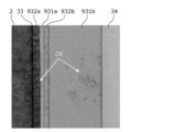
- FIG. 4 is a transmission electron microscope (TEM) image of the protective film of Comparative Example 1.
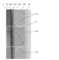
- FIGS. 5 and 6 are first and second TEM images of the protective film 3 according to this embodiment, respectively.
- FIG. 5 is an enlarged TEM image of the rectangular frame V shown in FIG. 6.
- FIG. 6 the boundary between the inner region R1 and the outer region R2 in the first protective films 31a and 31b is shown by a white dashed line.
- FIGS. 5 is an enlarged TEM image of the rectangular frame V shown in FIG. 6.
- FIG. 4 to 6 show the state of each protective film after an aging test was performed on each semiconductor light-emitting element. In the aging test, 1.4 W of continuous (CW) laser light was output to each semiconductor light-emitting element for 1000 hours.
- the black parts of the fifth protective film 931a, 931b shown in FIG. 4 and the first protective film 31a, 31b shown in FIG. 5 are photocrystallized regions CR. As shown in FIG. 4, the region of the fifth protective film 931a near the interface with the sixth protective film 932a and a part of the fifth protective film 931b are photocrystallized. As shown in FIG. 5 and FIG.
- the region indicated by the internal region R1 covering a wide range of the first protective film 31a and the first protective film 31b is photocrystallized.
- the first protective films 31a, 31b according to this embodiment have a larger amount of photocrystallization after the aging test than the fifth protective films 931a, 931b of Comparative Example 1.
- this photocrystallization mainly occurs in the internal region R1 including the region (optical path) through which the light emitted by each semiconductor light emitting element propagates and its vicinity.
- the inner region R1 of the first protective films 31a and 31b which includes the optical path, is photocrystallized, while the outer region R2 located outside the inner region R1 is not photocrystallized and remains amorphous. It is presumed that such photocrystallization increases the refractive index of the inner region R1 of the first protective films 31a and 31b. Note that photocrystallization was not confirmed in any of the protective films other than the first protective films 31a and 31b after the aging test.
- the photocrystallized region CR of the first protective film 31a is wider than that of the first protective film 31b.
- the first protective film 31a is photocrystallized even in a region farther from the optical path than the first protective film 31b.
- Figs. 7 and 8 are schematic diagrams showing photocrystallization and oxygen diffusion in the fifth protective film 931a of Comparative Example 1 and the first protective film 31a of this embodiment, respectively.
- FIG. 7 and 8 show each protective film immediately after it is formed
- the schematic diagram (b) shows the state of photocrystallization and oxygen diffusion of each protective film after a relatively short time (e.g., 500 hours) has elapsed since the start of operation of each semiconductor light-emitting element
- the schematic diagram (c) shows the state of photocrystallization and oxygen diffusion of each protective film after a long time (e.g., 5000 hours) has elapsed since the start of operation of each semiconductor light-emitting element.
- the fifth protective film 931a and the first protective film 31a are not irradiated with light immediately after deposition, so photocrystallization and oxygen diffusion do not occur.
- oxygen diffusion is dominant among oxygen diffusion and photocrystallization in the fifth protective film 931a after driving starts, so it takes a long time (e.g., 5000 hours) for the fifth protective film 931a to be photocrystallized after driving starts.
- the photocrystallized region of the fifth protective film 931a has the effect of suppressing oxygen diffusion, but photocrystallization takes a long time, so that the oxygen diffused in the fifth protective film 931a reaches the stacked structure 2 before the entire optical path of the fifth protective film 931a is photocrystallized.
- the nitride semiconductor of the stacked structure 2 is oxidized, increasing light absorption in the stacked structure 2, making the semiconductor light-emitting device of Comparative Example 1 more susceptible to COD.
- the entire optical path of the fifth protective film 931a is photocrystallized, so that oxygen diffused in the fifth protective film 931a can be prevented from reaching the laminated structure 2. In other words, it is possible to prevent the acceleration of characteristic deterioration due to further oxygen diffusion.
- the first protective film 31a after the start of operation, photocrystallization becomes dominant among oxygen diffusion and photocrystallization in the first protective film 31a, and the first protective film 31a is photocrystallized quickly (for example, after 100 hours). Therefore, as shown in the schematic diagram (b) of FIG. 8, since the first protective film 31a is photocrystallized, oxygen diffusion is suppressed in the photocrystallized region, and oxygen can be suppressed from reaching the stacked structure 2. Therefore, in this embodiment, the nitride semiconductor of the stacked structure 2 can be suppressed from being oxidized, and therefore light absorption in the stacked structure 2 can be suppressed. Therefore, the occurrence of COD in the semiconductor light emitting element 1 can be suppressed.
- the semiconductor light-emitting device 1 has first protective films 31a, 31b, which are aluminum oxide films doped with scandium, and thus has higher reliability than the semiconductor light-emitting device of Comparative Example 1.
- first protective films 31a, 31b which are aluminum oxide films doped with scandium, and thus has higher reliability than the semiconductor light-emitting device of Comparative Example 1.
- aluminum oxide films doped with scandium are used as the first protective films 31a, 31b, but the same effect can be obtained by using aluminum oxynitride films doped with scandium.
- the semiconductor light emitting devices according to Comparative Examples 2 and 3 are different from the semiconductor light emitting device 1 according to the present embodiment in that they use a seventh protective film made of Al 2 O 3 (Al 2 O 3 :Y) to which yttrium (Y) is added instead of the first protective films 31a and 31b of the protective film 3 of the semiconductor light emitting device 1 according to the present embodiment, and use an eighth protective film made of AlON (AlON:Y) to which yttrium is added instead of the second protective films 32a and 32b, but are the same in other respects.
- a seventh protective film made of Al 2 O 3 Al 2 O 3 :Y
- Y yttrium
- AlON AlON
- the yttrium concentrations in the seventh protective films of the semiconductor light emitting devices according to Comparative Examples 2 and 3 are 1.0% and 8.0%, respectively.
- the yttrium concentrations in the eighth protective films of the semiconductor light emitting devices according to Comparative Examples 2 and 3 are 1.0% and 8.0%, respectively.
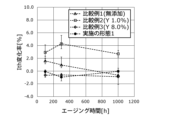
- FIG. 9 is a graph showing the relationship between the optical output degradation rate of each semiconductor light-emitting element of the present embodiment and Comparative Examples 1 to 3 and the aging time.
- the optical output degradation rate [%] is defined as (P1-P0) x 100/P0 using the optical output P0 before the aging test starts (i.e., aging time 0) and the optical output P1 after the aging test starts.
- FIG. 10 is a graph showing the relationship between the laser oscillation threshold current (Ith) change rate of each semiconductor light-emitting element of the present embodiment and Comparative Examples 1 to 3 and the aging time.
- Ith laser oscillation threshold current
- the Ith change rate [%] is defined as (Ith1-Ith0) x 100/Ith0 using the laser oscillation threshold current Ith0 before the aging test starts and the laser oscillation threshold current Ith1 after the aging test starts.
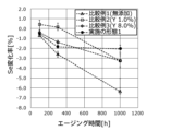
- FIG. 11 is a graph showing the relationship between the slope efficiency (Se) change rate of each semiconductor light-emitting element of the present embodiment and Comparative Examples 1 to 3 and the aging time.
- the Se change rate [%] is defined as (Se1-Se0) x 100/Se0, where Se0 is the slope efficiency before the aging test starts and Se1 is the slope efficiency after the aging test starts.
- the light output degradation rate after 300 hours of aging is greater than that of the semiconductor light-emitting devices of Comparative Examples 1 to 3, but the light output degradation rate after 1000 hours of aging is smaller than that of the semiconductor light-emitting devices of Comparative Examples 1 to 3.
- the laser oscillation threshold hardly changes even after 1000 hours of aging. Also, as shown in FIG.
- the Se change rate after 300 hours of aging is greater than that of the semiconductor light-emitting devices of Comparative Examples 2 and 3, but the light output degradation rate after 1000 hours of aging is smaller than that of the semiconductor light-emitting devices of Comparative Examples 1 to 3.
- this embodiment can realize a highly reliable semiconductor light-emitting element 1 that can suppress deterioration due to aging.
- Figs. 12 and 13 are schematic diagrams showing the shapes of the surface SF of the fifth protective film 931a of Comparative Example 1 and the first protective film 31a according to this embodiment, respectively.
- Figs. 12 and 13 also show the stacked structure 2, the third protective film 33, and the second protective film 32a.
- the dashed lines shown in Figs. 12 and 13 indicate the outer edges of the optical path.
- the film thickness of the first protective film 31a in the optical path becomes almost uniform. In other words, it is possible to suppress the decrease in flatness of the surface SF of the first protective film 31a in the optical path. Therefore, in the semiconductor light-emitting element 1 according to this embodiment, it is possible to suppress the disturbance of the FFP. In other words, in the semiconductor light-emitting element 1 according to this embodiment, it is possible to stabilize the FFP.
- the first protective films 31a, 31b in this embodiment may be amorphous or amorphous containing a crystalline phase.
- the energy applied to the laminated structure 2 during film formation can be reduced compared to when crystalline protective films are formed as the first protective films 31a and 31b. Therefore, damage to the laminated structure 2 during film formation of the first protective films 31a and 31b can be suppressed. At the same time, damage to the second protective film 32a and the third protective film 33 can also be suppressed. This can further increase the reliability of the semiconductor light emitting element 1.
- the concentration of scandium added to the first protective films 31a and 31b in this embodiment may be 10 at% or less.
- the protective film 3 may include a second protective film 32a disposed between the first end face 2F and the first protective film 31a, and the second protective film 32a may be a crystalline film made of a nitride or oxynitride of aluminum doped with scandium.
- the protective film 3 according to this embodiment includes a second protective film 32b disposed between the first end face 2F and the first protective film 31b, and the second protective film 32b may be a crystalline film made of a nitride or oxynitride of aluminum doped with scandium.
- each second protective film which is such a crystalline film
- each second protective film may be able to promote photocrystallization of each first protective film, or may be able to trap oxygen. This makes it possible to further suppress oxygen diffusion in each first protective film, and therefore further suppress oxidation of the stacked structure 2. Therefore, the reliability of the semiconductor light emitting element 1 can be further improved.
- the first protective films 31a and 31b can suppress oxygen diffusion to the second protective films 32a and 32b, thereby suppressing oxidation of the second protective films 32a and 32b.
- the crystal structure of the second protective films 32a and 32b may be a polycrystalline structure consisting of at least one of hexagonal and cubic crystals.
- the second protective films 32a and 32b may be hexagonal crystals oriented along the m-axis with respect to the first end face 2F.
- scandium which has a larger atomic radius and ionic radius than aluminum and gallium, is added to the second protective films 32a, 32b, which are hexagonal crystals, so that the lattice constant of the second protective films 32a, 32b approaches the lattice constant of the laminated structure 2.
- This may reduce dangling bonds at the interface between the laminated structure 2 and the protective film 3, and reduce crystal defects. By reducing dangling bonds in this way, crystal defects near the interface between the laminated structure 2 and the protective film 3 can be reduced, and light absorption can be reduced. This can further increase the reliability of the semiconductor light emitting element 1.
- the protective film 3 may include a plurality of laminated films 38a, 38b.
- Each of the laminated films 38a, 38b includes a first protective film 31a and a second protective film 32a in contact with the first protective film 31a.
- the laminated film 38b includes a first protective film 31b and a second protective film 32b in contact with the first protective film 31b.
- the reflectance of the protective film 3 can be easily controlled by including a first protective film with a low refractive index and a second protective film with a high refractive index that are arranged alternately.
- the protective film 3 includes a third protective film 33 in contact with the first end face 2F, and the third protective film 33 may be a silicon nitride film or an oxynitride film.
- the third protective film 33 By including such a third protective film 33 in the protective film 3, it is possible that dangling bonds at the interface between the laminated structure 2 and the protective film 3 can be terminated by the third protective film 33. This can improve adhesion between the laminated structure 2 and the protective film (in this embodiment, the second protective film 32a) adjacent to the laminated structure 2 via the third protective film 33. In addition, it is possible to reduce crystal defects near the interface between the laminated structure 2 and the protective film 3, and to reduce light absorption. Therefore, it is possible to further improve the reliability of the semiconductor light emitting element 1.
- the third protective film 33 may be amorphous.
- the protective film 3 may include a fourth protective film 34 which is a silicon oxide film, and the first protective films 31a and 31b may be disposed between the first end face 2F and the fourth protective film 34.
- the reflectance of the protective film 3 can be easily controlled by the protective film 3 including the fourth protective film 34, which has a smaller refractive index than the first protective films 31a and 31b.
- the first protective film 31b may be in contact with the fourth protective film 34.
- the fourth protective film 34 which is a silicon oxide film
- silicide Si
- This can increase the adhesion between the first protective film 31b and the fourth protective film 34. Therefore, the reliability of the semiconductor light emitting element 1 can be increased.
- the fourth protective film 34 may also be amorphous.
- FIG. 14 is a cross-sectional view showing the configuration of the protective film according to this embodiment.
- FIG. 14 also shows the stacked structure 2.
- FIG. 14 shows a cross section parallel to the resonance direction of light of the semiconductor light emitting element and the stacking direction of the stacked structure 2.
- the protective film according to this embodiment is the first protective film 31a, as shown in FIG. 14. In other words, the protective film according to this embodiment includes only the first protective film 31a.
- the first protective film 31a has a configuration similar to that of the first protective film 31a according to embodiment 1.
- the first protective film 31a contacts the first end surface 2F of the laminated structure 2.
- the first protective film 31a according to this embodiment also provides the same effects as the first protective films of the protective film 3 according to embodiment 1.
- the protective film according to this embodiment is composed only of the first protective film 31a, and therefore can be manufactured more easily than the protective film 3 according to the first embodiment.
- FIG. 15 is a cross-sectional view showing the configuration of the protective film 103 according to this embodiment.
- FIG. 15 also shows the stacked structure 2.
- FIG. 15 shows a cross section parallel to the resonance direction of light of the semiconductor light emitting element and the stacking direction of the stacked structure 2.
- the protective film 103 includes a plurality of laminated films 138a, 138b, and 138c, as shown in FIG. 15.
- the laminated film 138a includes a first protective film 31a and a second protective film 132a that is disposed between the first end face 2F and the first protective film 31a and in contact with the first protective film 31a.
- the laminated film 138b includes a first protective film 31b and a second protective film 132b that is disposed between the first end face 2F and the first protective film 31b and in contact with the first protective film 31b.
- the laminated film 138c includes a first protective film 31c and a second protective film 132c that is disposed between the first end face 2F and the first protective film 31c and in contact with the first protective film 31c.
- the first protective films 31a and 31b have the same configuration as the first protective films 31a and 31b according to the first embodiment.
- the first protective film 31c is an aluminum oxide film or an oxynitride film to which scandium has been added.
- the concentration of scandium added to the first protective film 31c is 10 at% or less.
- the first protective film 31c is amorphous or amorphous containing a crystalline phase, but may also be crystalline.
- the second protective films 132a, 132b, and 132c are crystalline films made of aluminum nitride or oxynitride, similar to the second protective films 32a and 32b in the first embodiment.
- the crystalline structure of the second protective films 132a, 132b, and 132c is a polycrystalline structure made of at least one of hexagonal and cubic crystals.
- the second protective films 132a, 132b, and 132c are hexagonal crystals oriented along the m-axis with respect to the first end face 2F.
- the second protective films 132a, 132b, and 132c in this embodiment are additive-free nitrides or oxynitrides that are not doped with scandium or the like.
- the first and second protective films included in the protective film 103 according to this embodiment also have the same effects as the first and second protective films of the protective film 3 according to embodiment 1.
- the protective film 103 includes three laminated films 138a, 138b, and 138c, which makes it even easier to control the reflectance of the protective film 103. Note that, although the protective film 103 includes three laminated films 138a, 138b, and 138c in this embodiment, it may include four or more laminated films.
- the protective film 103 according to this embodiment is composed only of the first protective films 31a, 31b, and 31c and the second protective films 132a, 132b, and 132c, and can therefore be manufactured more easily than the protective film 3 according to the first embodiment.
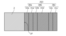
- FIG. 16 is a cross-sectional view showing the configuration of the protective film 203 according to this embodiment.
- FIG. 16 also shows the stacked structure 2.
- FIG. 16 shows a cross section parallel to the resonance direction of light of the semiconductor light emitting element and the stacking direction of the stacked structure 2.
- the protective film 203 includes a plurality of laminated films 38a, 38b, and 38c, as shown in FIG. 16.
- the laminated films 38a and 38b have the same configuration as the laminated films 38a and 38b according to embodiment 1.
- the laminated film 38c includes a first protective film 31c and a second protective film 32c that is disposed between the first end face 2F and the first protective film 31c and in contact with the first protective film 31c.
- the first protective film 31c according to this embodiment has the same configuration as the first protective film 31c according to embodiment 3.
- the second protective films 32a and 32b have the same configuration as the second protective films 32a and 32b according to embodiment 1.
- the second protective film 32c is a crystalline film made of aluminum nitride or oxynitride, like the second protective films 32a and 32b according to embodiment 1.
- the second protective film 32c is a nitride or oxynitride to which 10 at% or less of scandium has been added.
- the protective film 203 including the second protective films 32a, 32b, and 32c has the same effect as the protective film 103 according to the third embodiment.
- FIG. 17 is a cross-sectional view showing the configuration of the protective film 303 according to the present embodiment.
- FIG. 17 also shows the stacked structure 2.
- FIG. 17 shows a cross section parallel to the resonance direction of light of the semiconductor light emitting element and the stacking direction of the stacked structure 2.
- the protective film 303 in this embodiment includes a first protective film 31a and a third protective film 33, as shown in FIG. 17.
- the first protective film 31a has the same configuration as the first protective film 31a in embodiment 1.
- the third protective film 33 has a configuration similar to that of the third protective film 33 according to embodiment 1. In this embodiment, the third protective film 33 is in contact with the first protective film 31a.
- the protective film 303 according to this embodiment also exhibits the same effects as the first protective film 31a and the third protective film 33 according to embodiment 1.
- the protective film 303 according to this embodiment is composed of only two layers, the first protective film 31a and the third protective film 33, and therefore can be manufactured more easily than the protective film 3 according to the first embodiment.
- FIG. 18 is a cross-sectional view showing the configuration of the protective film 403 according to this embodiment.
- FIG. 18 also shows the stacked structure 2.
- FIG. 18 shows a cross section parallel to the resonance direction of light of the semiconductor light emitting element and the stacking direction of the stacked structure 2.
- the protective film 403 in this embodiment includes laminated films 38a, 38b, and 38c and a third protective film 33, as shown in FIG. 18.
- the third protective film 33 has a configuration similar to that of the third protective film 33 in embodiment 1.
- the protective film 403 according to this embodiment also provides the same effects as the protective film 203 according to the fourth embodiment.
- the protective film 403 according to this embodiment includes the third protective film 33, and thus has the same effect as the third protective film 33 in the protective film 3 according to embodiment 1.
- FIG. 19 is a cross-sectional view showing the configuration of the protective film 503 according to this embodiment.
- FIG. 19 also shows the stacked structure 2.
- FIG. 19 shows a cross section parallel to the resonance direction of light of the semiconductor light emitting element and the stacking direction of the stacked structure 2.
- the protective film 503 in this embodiment includes a first protective film 31a and a fourth protective film 34, as shown in FIG. 19.
- the first protective film 31a has a configuration similar to that of the first protective film 31a according to embodiment 1. In this embodiment, the first protective film 31a contacts the first end surface 2F.
- the fourth protective film 34 has the same configuration as the fourth protective film 34 according to embodiment 1.
- the fourth protective film 34 contacts the first protective film 31a.
- the protective film 503 according to this embodiment also exhibits the same effects as the first protective film 31a and the fourth protective film 34 according to embodiment 1.
- the protective film 503 according to this embodiment is composed of only two layers, the first protective film 31a and the fourth protective film 34, and therefore can be manufactured more easily than the protective film 3 according to the first embodiment.
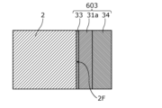
- FIG. 20 is a cross-sectional view showing the configuration of the protective film 603 according to this embodiment.
- FIG. 20 also shows the stacked structure 2.
- FIG. 20 shows a cross section parallel to the resonance direction of light of the semiconductor light emitting element and the stacking direction of the stacked structure 2.
- the protective film 603 in this embodiment includes a first protective film 31a, a third protective film 33, and a fourth protective film 34.
- the first protective film 31a has a configuration similar to that of the first protective film 31a according to embodiment 1. In this embodiment, the first protective film 31a is in contact with the third protective film 33 and the fourth protective film 34.
- the third protective film 33 has a configuration similar to that of the third protective film 33 according to embodiment 1.
- the third protective film 33 contacts the first end face 2F and the first protective film 31a.
- the fourth protective film 34 has the same configuration as the fourth protective film 34 according to embodiment 1.
- the fourth protective film 34 contacts the first protective film 31a.
- the protective film 603 according to this embodiment also exhibits the same effects as the first protective film 31a, the third protective film 33, and the fourth protective film 34 according to embodiment 1.
- the protective film 503 according to this embodiment is composed of only three layers, the first protective film 31a, the third protective film 33, and the fourth protective film 34, and therefore can be manufactured more easily than the protective film 3 according to the first embodiment.
- the configuration of the laminated structure 2 according to the present disclosure is not limited to the configuration examples shown in the above embodiments.
- the laminated structure 2 may be any laminated structure that includes a nitride semiconductor and has a first end face 2F and a second end face 2R that face each other and form a resonator. Furthermore, the light emitted by the laminated structure 2 does not have to be in the ultraviolet range.
- the semiconductor light-emitting element is a semiconductor laser element
- the semiconductor light-emitting element is not limited to a semiconductor laser element.
- the semiconductor light-emitting element may be a superluminescent diode.
- the protective film of the semiconductor light-emitting device includes a first protective film, it may include only a second protective film without including the first protective film.
- the semiconductor light-emitting device has a first end face and a second end face that face each other and form a resonator, and includes a stacked structure including a nitride semiconductor and a protective film disposed on the first end face, and the protective film includes a second protective film, and the first protective film may be a crystalline film made of an aluminum oxide film or oxynitride film to which scandium has been added.
- the protective film is disposed on both the first end surface 2F and the second end surface 2R, but it is sufficient that the protective film is disposed on at least one of the first end surface 2F and the second end surface 2R.
- each protective film disposed on the first end surface 2F may also be disposed on the second end surface 2R.
- the semiconductor light-emitting device is particularly useful as an external resonator type semiconductor light-emitting device that requires control of the reflectance of the end face, such as a high-output semiconductor light source for laser processing, a high-output light source for LDI (Laser Direct Imaging), or a light source for DDL (Direct Diode Laser).
- a high-output semiconductor light source for laser processing such as a high-output semiconductor light source for laser processing, a high-output light source for LDI (Laser Direct Imaging), or a light source for DDL (Direct Diode Laser).
- LDI Laser Direct Imaging
- DDL Direct Diode Laser
Landscapes
- Physics & Mathematics (AREA)
- Condensed Matter Physics & Semiconductors (AREA)
- General Physics & Mathematics (AREA)
- Electromagnetism (AREA)
- Optics & Photonics (AREA)
- Geometry (AREA)
- Semiconductor Lasers (AREA)
Priority Applications (3)
| Application Number | Priority Date | Filing Date | Title |
|---|---|---|---|
| CN202480038547.2A CN121285914A (zh) | 2023-06-13 | 2024-06-05 | 半导体发光元件 |
| JP2025527857A JPWO2024257659A1 (https=) | 2023-06-13 | 2024-06-05 | |
| US19/389,542 US20260074484A1 (en) | 2023-06-13 | 2025-11-14 | Semiconductor light-emitting element |
Applications Claiming Priority (2)
| Application Number | Priority Date | Filing Date | Title |
|---|---|---|---|
| JP2023097048 | 2023-06-13 | ||
| JP2023-097048 | 2023-06-13 |
Related Child Applications (1)
| Application Number | Title | Priority Date | Filing Date |
|---|---|---|---|
| US19/389,542 Continuation-In-Part US20260074484A1 (en) | 2023-06-13 | 2025-11-14 | Semiconductor light-emitting element |
Publications (1)
| Publication Number | Publication Date |
|---|---|
| WO2024257659A1 true WO2024257659A1 (ja) | 2024-12-19 |
Family
ID=93851890
Family Applications (1)
| Application Number | Title | Priority Date | Filing Date |
|---|---|---|---|
| PCT/JP2024/020448 Ceased WO2024257659A1 (ja) | 2023-06-13 | 2024-06-05 | 半導体発光素子 |
Country Status (4)
| Country | Link |
|---|---|
| US (1) | US20260074484A1 (https=) |
| JP (1) | JPWO2024257659A1 (https=) |
| CN (1) | CN121285914A (https=) |
| WO (1) | WO2024257659A1 (https=) |
Citations (5)
| Publication number | Priority date | Publication date | Assignee | Title |
|---|---|---|---|---|
| JP2004363320A (ja) * | 2003-06-04 | 2004-12-24 | Sharp Corp | 酸化物半導体発光素子 |
| JP2005166945A (ja) * | 2003-12-02 | 2005-06-23 | Nichia Chem Ind Ltd | 半導体レーザ素子の製造方法及び半導体レーザ素子 |
| JP2011119540A (ja) * | 2009-12-04 | 2011-06-16 | Panasonic Corp | 窒化物半導体レーザ素子 |
| WO2014002339A1 (ja) * | 2012-06-29 | 2014-01-03 | パナソニック株式会社 | 窒化物半導体発光素子 |
| JP2023005918A (ja) * | 2021-06-29 | 2023-01-18 | ヌヴォトンテクノロジージャパン株式会社 | 窒化物半導体発光素子 |
-
2024
- 2024-06-05 WO PCT/JP2024/020448 patent/WO2024257659A1/ja not_active Ceased
- 2024-06-05 CN CN202480038547.2A patent/CN121285914A/zh active Pending
- 2024-06-05 JP JP2025527857A patent/JPWO2024257659A1/ja active Pending
-
2025
- 2025-11-14 US US19/389,542 patent/US20260074484A1/en active Pending
Patent Citations (5)
| Publication number | Priority date | Publication date | Assignee | Title |
|---|---|---|---|---|
| JP2004363320A (ja) * | 2003-06-04 | 2004-12-24 | Sharp Corp | 酸化物半導体発光素子 |
| JP2005166945A (ja) * | 2003-12-02 | 2005-06-23 | Nichia Chem Ind Ltd | 半導体レーザ素子の製造方法及び半導体レーザ素子 |
| JP2011119540A (ja) * | 2009-12-04 | 2011-06-16 | Panasonic Corp | 窒化物半導体レーザ素子 |
| WO2014002339A1 (ja) * | 2012-06-29 | 2014-01-03 | パナソニック株式会社 | 窒化物半導体発光素子 |
| JP2023005918A (ja) * | 2021-06-29 | 2023-01-18 | ヌヴォトンテクノロジージャパン株式会社 | 窒化物半導体発光素子 |
Also Published As
| Publication number | Publication date |
|---|---|
| JPWO2024257659A1 (https=) | 2024-12-19 |
| US20260074484A1 (en) | 2026-03-12 |
| CN121285914A (zh) | 2026-01-06 |
Similar Documents
| Publication | Publication Date | Title |
|---|---|---|
| US8885681B2 (en) | Semiconductor laser device | |
| US7773648B2 (en) | Semiconductor device and method for manufacturing the same | |
| US8891568B2 (en) | Laser diode device and method of manufacturing laser diode device | |
| US20090010292A1 (en) | Nitride-based semiconductor laser device | |
| JP7716389B2 (ja) | 半導体レーザ装置及び半導体レーザ装置の製造方法 | |
| JP7296934B2 (ja) | 窒化物半導体レーザ素子及び照明光源モジュール | |
| KR100689782B1 (ko) | 반도체 발광 소자 및 그 제조 방법 | |
| CN104995805A (zh) | 半导体光元件、半导体激光元件、及其制造方法、和半导体激光模块元件以及半导体元件的制造方法 | |
| US7515621B2 (en) | Nitride semiconductor laser element | |
| JP2003204122A5 (https=) | ||
| US20010010373A1 (en) | Semiconductor light emitting device | |
| JP2005327783A (ja) | 半導体レーザ | |
| JP2010212499A (ja) | 半導体レーザ素子 | |
| US20090059986A1 (en) | Semiconductor light emitting element | |
| CN1305192C (zh) | 具有高阶模式吸收层的半导体激光二极管 | |
| JP2025129325A (ja) | 窒化物半導体レーザ素子 | |
| JP3646302B2 (ja) | 半導体レーザ | |
| WO2024257659A1 (ja) | 半導体発光素子 | |
| CN118679654A (zh) | 氮化物系半导体发光元件 | |
| JP2011023493A (ja) | 半導体レーザ | |
| US20100238963A1 (en) | Gallium nitride based semiconductor laser device | |
| JP5966381B2 (ja) | 半導体レーザおよびその製造方法 | |
| US20240396303A1 (en) | Vertical cavity surface emitting laser element | |
| JP2005327907A (ja) | 半導体レーザ素子 | |
| JP2006339311A (ja) | 半導体レーザ |
Legal Events
| Date | Code | Title | Description |
|---|---|---|---|
| 121 | Ep: the epo has been informed by wipo that ep was designated in this application |
Ref document number: 24823278 Country of ref document: EP Kind code of ref document: A1 |
|
| ENP | Entry into the national phase |
Ref document number: 2025527857 Country of ref document: JP Kind code of ref document: A |
|
| WWE | Wipo information: entry into national phase |
Ref document number: 2025527857 Country of ref document: JP |
|
| NENP | Non-entry into the national phase |
Ref country code: DE |