WO2024257327A1 - 電力変換装置 - Google Patents
電力変換装置 Download PDFInfo
- Publication number
- WO2024257327A1 WO2024257327A1 PCT/JP2023/022368 JP2023022368W WO2024257327A1 WO 2024257327 A1 WO2024257327 A1 WO 2024257327A1 JP 2023022368 W JP2023022368 W JP 2023022368W WO 2024257327 A1 WO2024257327 A1 WO 2024257327A1
- Authority
- WO
- WIPO (PCT)
- Prior art keywords
- converter
- voltage
- capacitor
- sub
- power conversion
- Prior art date
- Legal status (The legal status is an assumption and is not a legal conclusion. Google has not performed a legal analysis and makes no representation as to the accuracy of the status listed.)
- Ceased
Links
Images




Classifications
-
- H—ELECTRICITY
- H02—GENERATION; CONVERSION OR DISTRIBUTION OF ELECTRIC POWER
- H02M—APPARATUS FOR CONVERSION BETWEEN AC AND AC, BETWEEN AC AND DC, OR BETWEEN DC AND DC, AND FOR USE WITH MAINS OR SIMILAR POWER SUPPLY SYSTEMS; CONVERSION OF DC OR AC INPUT POWER INTO SURGE OUTPUT POWER; CONTROL OR REGULATION THEREOF
- H02M7/00—Conversion of AC power input into DC power output; Conversion of DC power input into AC power output
- H02M7/42—Conversion of DC power input into AC power output without possibility of reversal
- H02M7/44—Conversion of DC power input into AC power output without possibility of reversal by static converters
- H02M7/48—Conversion of DC power input into AC power output without possibility of reversal by static converters using discharge tubes with control electrode or semiconductor devices with control electrode
- H02M7/483—Converters with outputs that each can have more than two voltages levels
- H02M7/487—Neutral point clamped inverters
-
- H—ELECTRICITY
- H02—GENERATION; CONVERSION OR DISTRIBUTION OF ELECTRIC POWER
- H02M—APPARATUS FOR CONVERSION BETWEEN AC AND AC, BETWEEN AC AND DC, OR BETWEEN DC AND DC, AND FOR USE WITH MAINS OR SIMILAR POWER SUPPLY SYSTEMS; CONVERSION OF DC OR AC INPUT POWER INTO SURGE OUTPUT POWER; CONTROL OR REGULATION THEREOF
- H02M1/00—Details of apparatus for conversion
- H02M1/0003—Details of control, feedback or regulation circuits
- H02M1/0025—Arrangements for modifying reference values, feedback values or error values in the control loop of a converter
-
- H—ELECTRICITY
- H02—GENERATION; CONVERSION OR DISTRIBUTION OF ELECTRIC POWER
- H02M—APPARATUS FOR CONVERSION BETWEEN AC AND AC, BETWEEN AC AND DC, OR BETWEEN DC AND DC, AND FOR USE WITH MAINS OR SIMILAR POWER SUPPLY SYSTEMS; CONVERSION OF DC OR AC INPUT POWER INTO SURGE OUTPUT POWER; CONTROL OR REGULATION THEREOF
- H02M1/00—Details of apparatus for conversion
- H02M1/0067—Converter structures employing plural converter units, other than for parallel operation of the units on a single load
- H02M1/007—Plural converter units in cascade
-
- H—ELECTRICITY
- H02—GENERATION; CONVERSION OR DISTRIBUTION OF ELECTRIC POWER
- H02M—APPARATUS FOR CONVERSION BETWEEN AC AND AC, BETWEEN AC AND DC, OR BETWEEN DC AND DC, AND FOR USE WITH MAINS OR SIMILAR POWER SUPPLY SYSTEMS; CONVERSION OF DC OR AC INPUT POWER INTO SURGE OUTPUT POWER; CONTROL OR REGULATION THEREOF
- H02M1/00—Details of apparatus for conversion
- H02M1/0095—Hybrid converter topologies, e.g. NPC mixed with flying capacitor, thyristor converter mixed with MMC or charge pump mixed with buck
-
- H—ELECTRICITY
- H02—GENERATION; CONVERSION OR DISTRIBUTION OF ELECTRIC POWER
- H02M—APPARATUS FOR CONVERSION BETWEEN AC AND AC, BETWEEN AC AND DC, OR BETWEEN DC AND DC, AND FOR USE WITH MAINS OR SIMILAR POWER SUPPLY SYSTEMS; CONVERSION OF DC OR AC INPUT POWER INTO SURGE OUTPUT POWER; CONTROL OR REGULATION THEREOF
- H02M1/00—Details of apparatus for conversion
- H02M1/38—Means for preventing simultaneous conduction of switches
-
- H—ELECTRICITY
- H02—GENERATION; CONVERSION OR DISTRIBUTION OF ELECTRIC POWER
- H02M—APPARATUS FOR CONVERSION BETWEEN AC AND AC, BETWEEN AC AND DC, OR BETWEEN DC AND DC, AND FOR USE WITH MAINS OR SIMILAR POWER SUPPLY SYSTEMS; CONVERSION OF DC OR AC INPUT POWER INTO SURGE OUTPUT POWER; CONTROL OR REGULATION THEREOF
- H02M1/00—Details of apparatus for conversion
- H02M1/42—Circuits or arrangements for compensating for or adjusting power factor in converters or inverters
- H02M1/4208—Arrangements for improving power factor of AC input
- H02M1/4216—Arrangements for improving power factor of AC input operating from a three-phase input voltage
-
- H—ELECTRICITY
- H02—GENERATION; CONVERSION OR DISTRIBUTION OF ELECTRIC POWER
- H02M—APPARATUS FOR CONVERSION BETWEEN AC AND AC, BETWEEN AC AND DC, OR BETWEEN DC AND DC, AND FOR USE WITH MAINS OR SIMILAR POWER SUPPLY SYSTEMS; CONVERSION OF DC OR AC INPUT POWER INTO SURGE OUTPUT POWER; CONTROL OR REGULATION THEREOF
- H02M1/00—Details of apparatus for conversion
- H02M1/42—Circuits or arrangements for compensating for or adjusting power factor in converters or inverters
- H02M1/4208—Arrangements for improving power factor of AC input
- H02M1/4225—Arrangements for improving power factor of AC input using a non-isolated boost converter
-
- H—ELECTRICITY
- H02—GENERATION; CONVERSION OR DISTRIBUTION OF ELECTRIC POWER
- H02M—APPARATUS FOR CONVERSION BETWEEN AC AND AC, BETWEEN AC AND DC, OR BETWEEN DC AND DC, AND FOR USE WITH MAINS OR SIMILAR POWER SUPPLY SYSTEMS; CONVERSION OF DC OR AC INPUT POWER INTO SURGE OUTPUT POWER; CONTROL OR REGULATION THEREOF
- H02M1/00—Details of apparatus for conversion
- H02M1/42—Circuits or arrangements for compensating for or adjusting power factor in converters or inverters
- H02M1/4208—Arrangements for improving power factor of AC input
- H02M1/4233—Arrangements for improving power factor of AC input using a bridge converter comprising active switches
-
- H—ELECTRICITY
- H02—GENERATION; CONVERSION OR DISTRIBUTION OF ELECTRIC POWER
- H02M—APPARATUS FOR CONVERSION BETWEEN AC AND AC, BETWEEN AC AND DC, OR BETWEEN DC AND DC, AND FOR USE WITH MAINS OR SIMILAR POWER SUPPLY SYSTEMS; CONVERSION OF DC OR AC INPUT POWER INTO SURGE OUTPUT POWER; CONTROL OR REGULATION THEREOF
- H02M7/00—Conversion of AC power input into DC power output; Conversion of DC power input into AC power output
- H02M7/42—Conversion of DC power input into AC power output without possibility of reversal
- H02M7/44—Conversion of DC power input into AC power output without possibility of reversal by static converters
- H02M7/48—Conversion of DC power input into AC power output without possibility of reversal by static converters using discharge tubes with control electrode or semiconductor devices with control electrode
- H02M7/483—Converters with outputs that each can have more than two voltages levels
- H02M7/4833—Capacitor voltage balancing
-
- H—ELECTRICITY
- H02—GENERATION; CONVERSION OR DISTRIBUTION OF ELECTRIC POWER
- H02M—APPARATUS FOR CONVERSION BETWEEN AC AND AC, BETWEEN AC AND DC, OR BETWEEN DC AND DC, AND FOR USE WITH MAINS OR SIMILAR POWER SUPPLY SYSTEMS; CONVERSION OF DC OR AC INPUT POWER INTO SURGE OUTPUT POWER; CONTROL OR REGULATION THEREOF
- H02M7/00—Conversion of AC power input into DC power output; Conversion of DC power input into AC power output
- H02M7/42—Conversion of DC power input into AC power output without possibility of reversal
- H02M7/44—Conversion of DC power input into AC power output without possibility of reversal by static converters
- H02M7/48—Conversion of DC power input into AC power output without possibility of reversal by static converters using discharge tubes with control electrode or semiconductor devices with control electrode
- H02M7/483—Converters with outputs that each can have more than two voltages levels
- H02M7/4835—Converters with outputs that each can have more than two voltages levels comprising two or more cells, each including a switchable capacitor, the capacitors having a nominal charge voltage which corresponds to a given fraction of the input voltage, and the capacitors being selectively connected in series to determine the instantaneous output voltage
-
- H—ELECTRICITY
- H02—GENERATION; CONVERSION OR DISTRIBUTION OF ELECTRIC POWER
- H02M—APPARATUS FOR CONVERSION BETWEEN AC AND AC, BETWEEN AC AND DC, OR BETWEEN DC AND DC, AND FOR USE WITH MAINS OR SIMILAR POWER SUPPLY SYSTEMS; CONVERSION OF DC OR AC INPUT POWER INTO SURGE OUTPUT POWER; CONTROL OR REGULATION THEREOF
- H02M7/00—Conversion of AC power input into DC power output; Conversion of DC power input into AC power output
- H02M7/42—Conversion of DC power input into AC power output without possibility of reversal
- H02M7/44—Conversion of DC power input into AC power output without possibility of reversal by static converters
- H02M7/48—Conversion of DC power input into AC power output without possibility of reversal by static converters using discharge tubes with control electrode or semiconductor devices with control electrode
- H02M7/53—Conversion of DC power input into AC power output without possibility of reversal by static converters using discharge tubes with control electrode or semiconductor devices with control electrode using devices of a triode or transistor type requiring continuous application of a control signal
- H02M7/537—Conversion of DC power input into AC power output without possibility of reversal by static converters using discharge tubes with control electrode or semiconductor devices with control electrode using devices of a triode or transistor type requiring continuous application of a control signal using semiconductor devices only, e.g. single switched pulse inverters
- H02M7/5387—Conversion of DC power input into AC power output without possibility of reversal by static converters using discharge tubes with control electrode or semiconductor devices with control electrode using devices of a triode or transistor type requiring continuous application of a control signal using semiconductor devices only, e.g. single switched pulse inverters in a bridge configuration
- H02M7/53871—Conversion of DC power input into AC power output without possibility of reversal by static converters using discharge tubes with control electrode or semiconductor devices with control electrode using devices of a triode or transistor type requiring continuous application of a control signal using semiconductor devices only, e.g. single switched pulse inverters in a bridge configuration with automatic control of output voltage or current
Definitions
- This disclosure relates to a power conversion device.
- Power conversion devices such as inverters and converters that convert power between direct current and three-phase alternating current are used for a variety of applications, and there is a demand for miniaturization and weight reduction. For this reason, multilevel power conversion devices (see, for example, Patent Document 1 and Non-Patent Document 1) are used to reduce the volume of passive components such as capacitors, inductors, and resistors that occupy the power conversion device.
- the semiconductor switching elements and smoothing capacitors bear a voltage lower than the DC voltage, making it possible to use low-voltage semiconductor switching elements and low-voltage capacitors, thereby achieving high power output and high power density.
- the semiconductor switching elements and smoothing capacitors bear a voltage lower than the DC voltage, making it possible to use low-voltage semiconductor switching elements and low-voltage capacitors, thereby achieving high power output and high power density.
- it is possible to output multilevel voltages by increasing the number of voltage levels, it is possible to reduce the energy stored in the inductor, making it possible to realize a smaller inductor with lower loss.
- JP 2021-100363 A (paragraphs 0020 to 0025, FIG. 1)
- This disclosure discloses technology to solve the problems described above, and aims to obtain a power conversion device that can output multilevel voltages by applying low-voltage semiconductor switching elements without increasing the size and weight of the device.
- the power conversion device disclosed herein is characterized by comprising an inductor provided for each phase on the AC side, a main converter having one end connected to the inductor and the other end with a DC positive pole, a DC negative pole, and a DC neutral point, a capacitor circuit having a positive pole, a DC negative pole, and a DC neutral point connected to the DC side, a sub-converter composed of a capacitor and a plurality of semiconductor switching elements, connected between the neutral point of the capacitor circuit and the neutral point of the main converter, the capacitor voltage changing according to the combination of the opening and closing settings of the plurality of semiconductor switching elements, and a control unit that controls the operation of the main converter and the sub-converter.
- the power conversion device disclosed herein can apply low-voltage semiconductor switching elements to the sub-converter, making it possible to obtain a power conversion device capable of outputting multilevel voltages without increasing the size and weight of the device.
- 1A and 1B are a circuit diagram for explaining the configuration of a power conversion device according to a first embodiment and a circuit diagram for explaining the configuration of a submodule that constitutes a power conversion circuit, respectively.
- 1 is a circuit diagram for explaining a power conversion circuit for one phase of a power conversion device according to a first embodiment
- 4 is a table showing output terminal voltages and switch settings for each switching state in the power conversion device according to the first embodiment.
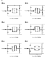
- FIG. 4A to 4F are diagrams illustrating conduction paths for each switching state in a power conversion circuit for one phase of the power conversion device according to the first embodiment.
- FIG. 1 is a tabular diagram showing the output voltage for each output end voltage and current direction for each switching state in a power conversion device according to the first embodiment, the charge/discharge state of the capacitor of the sub-converter, and the charge/discharge state of the positive side capacitor and the negative side capacitor.
- 2 is a circuit diagram for explaining a configuration of a control unit constituting the power conversion device according to the first embodiment.
- FIG. 7A and 7B are schematic diagrams showing transitions of modes and switching states when the current direction is positive and negative, respectively, in the power conversion device according to the first embodiment.
- 1 is a schematic diagram showing the transition of modes and switching states when the current direction is positive in a power conversion device according to a first embodiment, together with a conduction path in a power conversion circuit for one phase.
- FIG. 1 is a schematic diagram showing the transition of modes and switching states when the current direction is negative in a power conversion device according to a first embodiment, together with a conduction path in a power conversion circuit for one phase.
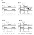
- FIG. 10A to 10D are diagrams showing time series changes in the modes set when the power conversion device is not provided with a zero voltage generating unit and when it is provided with a zero voltage generating unit when the current is positive and negative, respectively.
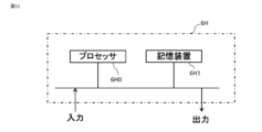
- 2 is a block diagram showing an example of a hardware configuration of a control unit constituting a power conversion device according to the present disclosure.
- FIG. 1 is a schematic diagram showing the transition of modes and switching states when the current direction is negative in a power conversion device according to a first embodiment, together with a conduction path in a power conversion circuit for one phase.
- FIG. 10A to 10D are diagrams showing time series changes in the modes set when the power conversion device is not provided with a zero voltage generating unit and when it is provided with a zero voltage generating unit when the current is positive and
- Figures 1A to 10D are intended to explain the configuration and operation of the power conversion device of embodiment 1, where Figure 1A is a circuit diagram for explaining the configuration of the power conversion device, Figure 1B is a circuit diagram of a sub-module that constitutes a sub-converter of a power conversion circuit, and Figure 2 is a circuit diagram for explaining a power conversion circuit for one phase when a sub-converter is constituted using one sub-module shown in Figure 1B for each phase.
- FIG. 3 is a table showing the output terminal voltage and switch opening/closing (on/off) settings for each switching state in the power conversion circuit for one phase shown in FIG. 2, while FIGS. 4A to 4F are diagrams showing the conduction paths for each switching state shown in FIG. 3 in the power conversion circuit for one phase shown in FIG. 2, and FIG. 5 is a table showing the output voltage for the output terminal voltage and current direction for each switching state shown in FIG. 3, the charge/discharge state of the sub-converter capacitor, and the charge/discharge state of the positive and negative capacitors. Note that in FIGS. 4A to 4F, the power conversion circuit itself is drawn with thin lines to highlight the current paths. The same applies to FIGS. 8 and 9, which will be described later.
- FIG. 6 is a circuit diagram for explaining the configuration of the control unit that controls the switching of the above-mentioned switching states
- FIG. 7A is a schematic diagram showing the transitions of the mode and switching state together with the set values when the current direction is positive
- FIG. 7B is a schematic diagram showing the transitions of the mode and switching state together with the set values when the current direction is negative. Note that in FIGS. 7A and 7B, from the left, the mode, the output terminal voltage, and the open/closed state of each of the four switches are listed in that order.
- Figure 8 is a schematic diagram corresponding to Figure 7A, which shows the transition of the mode and switching state together with the conduction path in the power conversion circuit for one phase when the current direction is positive
- Figure 9 is a schematic diagram corresponding to Figure 7B, which shows the transition of the mode and switching state together with the conduction path in the power conversion circuit for one phase when the current direction is negative.
- Figures 10A and 10B show the time series changes in the mode set for the switching elements in the submodule when the current is positive and when a zero voltage generator is not provided and when a zero voltage generator is provided, respectively.
- Figures 10C and 10D show the time series changes in the mode set for the switching elements in the submodule when the current is negative and when a zero voltage generator is not provided and when a zero voltage generator is provided, respectively.
- the power conversion device 10 of the present disclosure includes a power conversion circuit 1 having DC side terminals P, O, N that are connected to a DC power source or DC equipment, and AC side terminals R, S, T that are connected to an AC power source or AC equipment, as shown in FIG. 1A, and a control unit 6 that controls the operation of the power conversion circuit.
- the power conversion circuit 1 is arranged in the following order from the AC terminals (R, S, T) to the DC terminals (P, O, N): inductor 2, main converter 3, capacitor circuit 5.
- the sub-modules 7 shown in FIG. 1B are connected in series, and the sub-converter 4 is arranged between the neutral point O of each of the main converter 3 and the capacitor circuit 5.
- the main converter 3 By outputting a multi-level voltage from the AC output terminals (R, S, T) of the main converter 3, a voltage equal to the difference between the multi-level voltage and the AC terminal voltage is applied to the inductor 2 connected between the main converter 3 and the AC terminals (R, S, T).
- the sub-converter 4 is connected between the neutral point O of the DC terminal and the DC terminal of the main converter 3.
- the terminals of the main converter 3 are connected to the positive terminal P and negative terminal N of the DC terminal, respectively.
- the main converter 3 can output a multi-level voltage by outputting voltages equivalent to the positive voltage, negative voltage, and output terminal voltage of the sub-converter 4.
- the main converter 3 shows a power conversion circuit 1 capable of bidirectional power conversion using an active neutral point clamping method, but it may be configured to be capable of unidirectional power conversion only. In that case, the semiconductor switching elements of the main converter 3 can be changed to diodes to reduce the number of semiconductor switching elements.
- the sub-converter 4 is configured such that one sub-module 7 is a two-level full-bridge converter containing at least one capacitor, and at least one sub-module 7 is connected between the main converter 3 and the neutral point O of each of the capacitor circuits 5. If the neutral point voltage is the reference potential (GND, 0V), the output terminal voltage of the sub-converter 4 is the positive voltage, negative voltage, or 0V of the capacitor voltage Vsx of the sub-converter 4.
- the control unit 6 controls the opening and closing (off and on) of the switches of the main converter 3 and the sub-converter 4 based on information such as the AC output terminal voltages vr, vs, vt, the positive capacitor voltage Vmp, the negative capacitor voltage Vmn, the capacitor voltages Vsr, Vss, Vst (indicated as "Vsx" in Figure 1B) of the sub-converter 4, and the inductor currents ir, is, it.
- the main converter 3 and sub-converter 4 are not limited to the illustrated configuration, and may be of a two-level type, diode clamp type, flying capacitor type, T-type type, neutral point clamp type, etc., and may have other numbers of output levels instead of being limited to two or three levels.
- the main converter 3 must be configured to be connectable to a neutral point, and the sub-converter 4 is connected between the neutral point connection point of the main converter 3 and the neutral point of the capacitor circuit 5.
- the capacitor Csx of the sub-converter 4 may be an external power source such as a battery. When limited to unidirectional power conversion from AC to DC only, some of the semiconductor switching elements of the main converter 3 and sub-converter 4 may be changed to diodes.
- the semiconductor switching elements may be silicon (Si) or silicon carbide (SiC)-based MOSFETs (Metal-Oxide-Semiconductor Field-Effect Transistors), IGBTs (Insulated Gate Bipolar Transistors), as well as gallium nitride (GaN)-based power transistors and gallium oxide (GaO)-based power transistors.
- SiC silicon carbide
- MOSFETs Metal-Oxide-Semiconductor Field-Effect Transistors
- IGBTs Insulated Gate Bipolar Transistors
- GaN gallium nitride
- GaO gallium oxide
- the semiconductor switching elements may be a mixture of the above-mentioned silicon-based IGBTs and silicon carbide-based MOSFETs.
- inductor 2 connected between the AC terminal and the main converter 3 has at least one inductor L
- other passive components may be connected in series or parallel to the inductor 2.
- An LC filter, an LCL filter, etc. may be connected to remove harmonic switching noise.
- a damping circuit may also be provided to suppress the resonance phenomenon of the filter.
- the control unit 6 may have one or more controllers (controllers). For example, separate controllers may be applied to the main converter 3 and the sub-converter 4, or separate controllers may be used for the main converter 3 and the sub-converter 4 corresponding to each phase. Communication between the controllers may be either wired or wireless. In addition, the current detection value, voltage detection value, temperature detection value, gate signal, etc. of the power conversion circuit 1 may be connected to the control unit 6 by wire or wirelessly.
- the control unit 6 is composed of a CPU (Central Processing Unit), DSP (Digital Signal Processor), FPGA (Field-Programmable Gate Array), analog circuits, etc. Control may be applied so that the positive and negative voltages become the same voltage.
- the differential voltage between the positive and negative voltages is controlled to be zero, and the capacitor voltage Vsx of the sub-converter 4 is controlled to a predetermined voltage.
- the voltage control of the control unit 6 is, for example, proportional-integral control (PI) that brings the target voltage closer to the voltage detected by the voltage detection means.
- PI proportional-integral control
- the voltage detection means may directly detect the voltages across the positive and negative capacitors Cmp and Cmn as the positive and negative voltages.
- the negative and positive voltages may be estimated by subtracting the positive and negative capacitor voltages Vmp and Vmn from the voltages at the positive and negative terminals.
- the capacitor voltage Vsx of the sub-converter 4 may be estimated from the capacitor current value. To reduce the number of voltage sensors, the capacitor voltage Vsx of the sub-converter 4 may be estimated from the switching patterns of the main converter 3 and the sub-converter 4, the inductor currents ir, is, it, the positive and negative voltages, etc.
- the control unit 6 may detect the inductor currents ir, is, and it, perform dq (direct/quadrature) conversion, and control the dq converted current by PI control or the like.
- the inductor currents of all three phases may be detected.
- the inductor currents of two phases may be detected, and the current of the third phase may be calculated based on Kirchhoff's first law.
- the AC voltages of all three phases may be detected, and the phases may be synchronized by a PLL (phase locked loop).
- the AC voltage of only one phase may be detected, and the undetected AC voltage may be calculated by utilizing the 120 degree phase shift between the phases.
- the inductor currents ir is, it may be estimated from the inductor voltage, the AC side terminal voltage, the main converter output voltage command value in the control unit 6, etc.
- a device consisting of passive components, electronic components, semiconductor switching elements, etc. may be connected to the AC terminal side, and the output terminal from this device may be connected to the DC side terminal.
- a common mode filter, a normal mode filter, a submodule, etc. may be connected.
- a terminal output from a device such as the one described above that is connected to the DC terminal may be connected to the AC terminal.
- a motor, a generator, an AC system a load made up of passive components, or something that behaves like a current source or voltage source may be connected.
- a DC terminal for example, a solar cell, a fuel cell, a storage battery, a load made up of passive components, an LED (Light-Emitting Diode), a power conversion device, or something that behaves like a current source or voltage source may be connected.
- the AC terminal side is shown as three-phase, it may be single-phase or multi-phase, and there is no restriction on the phase wiring system. If it is single-phase, a half-bridge configuration or a full-bridge configuration may be considered. Even in the case of three phase, a V-connection method may be used in which one phase is connected to the AC terminal and the neutral point.
- the voltages of the submodules 7 may all be the same voltage or different voltages.
- the modulation method of the submodules 7 may be any known modulation method used in single-phase circuits, such as bipolar modulation, unipolar modulation, or hybrid modulation.
- the switching frequency of the main converter 3 may be set to the fundamental frequency of the AC side to reduce switching loss.
- the switching frequencies of the main converter 3 and sub-converter 4 may be set to different frequencies to reduce switching loss.
- a one-pulse voltage may be output from the main converter 3, and control may be applied in which the sub-converter 4 compensates for the differential voltage.
- the absolute value of the voltage output by the sub-converter 4 must be lower than the absolute values of the positive and negative voltages.
- the circuit diagram of the power conversion circuit 1x for one phase is as shown in Fig. 2.
- the switching elements (elements S x1 to S x4 ) corresponding to the main converter 3 are configured as a T-type type, but they may be configured as a diode clamp type, a flying capacitor type, a neutral point clamp type, or the like.
- Each of the six switching states determines the opening and closing, i.e., switch settings, of the switching elements (elements S x1 to S x4 ) that constitute the main converter 3 and the switching elements (elements S x7 to S x10 ) that constitute the sub-converter 4. Note that in the tabular form of Fig. 3 , from the left, the switching state, the output end voltage Vxo, and the switch settings of each of the switching elements (elements S x1 to S x4 , S x7 to S x10 ) (on (closed) is "1", off (open) is "0") are shown.
- FIGS. 4A to 4F show the conduction paths within the power conversion circuit 1x in each of the six switching states shown in FIG. 3.
- the current direction from AC to DC (to the right) is considered positive.
- FIGS. 4A to 4F show the case where the current direction is positive.
- Switching state 1 is when the converter output terminal voltage Vxo is +Vmp. In switching state 1, as shown in FIG. 4A, no current flows into the capacitor Csx of the submodule 7, so the capacitor voltage Vsx does not fluctuate. On the other hand, in the capacitor circuit 5 on the DC terminal side, current flows into the capacitors Cmp and Cmn, so the capacitor voltages Vmp and Vmn increase.
- Switching state 2 is when the converter output terminal voltage Vxo is +Vsx.
- switching state 2 as shown in FIG. 4B, current flows into capacitor Csx of submodule 7, causing the capacitor voltage Vsx to increase.
- capacitor circuit 5 current flows out of capacitor Cmp, causing the capacitor voltage Vmp to decrease, and current flows into capacitor Cmn, causing the capacitor voltage Vmn to increase.
- Switching state 3 is when the converter output terminal voltage Vxo is 0V. In switching state 3, as shown in FIG. 4C, no current flows through capacitor Csx of submodule 7, so the capacitor voltage Vsx does not change. On the other hand, in capacitor circuit 5, current flows out of capacitor Cmp, decreasing the capacitor voltage Vmp, and current flows into capacitor Cmn, increasing the capacitor voltage Vmn.
- Switching state 4 is when the converter output terminal voltage Vxo is 0V.
- switching state 4 as shown in FIG. 4D, no current flows through capacitor Csx of submodule 7, so the capacitor voltage Vsx does not change.
- capacitor circuit 5 current flows out of capacitor Cmp, decreasing the capacitor voltage Vmp, and current flows into capacitor Cmn, increasing the capacitor voltage Vmn.
- Switching state 5 is when the converter output terminal voltage Vxo is -Vsx.
- switching state 5 as shown in FIG. 4E, current flows out of capacitor Csx of submodule 7, causing the capacitor voltage Vsx to decrease.
- capacitor circuit 5 current flows out of capacitor Cmp, causing the capacitor voltage Vmp to decrease, and current flows into capacitor Cmn, causing the capacitor voltage Vmn to increase.
- Switching state 6 is when the converter output terminal voltage Vxo is -Vmp. In switching state 6, as shown in FIG. 4F, no current flows into the capacitor Csx of the submodule 7, so the capacitor voltage Vsx does not fluctuate. On the other hand, in the capacitor circuit 5, current flows out of the capacitors Cmp and Cmn, so the capacitor voltages Vmp and Vmn decrease.
- Figure 5 shows in table format the converter output terminal voltage Vxo for the switching state and current direction, the current direction, the charge/discharge state of the capacitor Csx of the sub-converter 4, the charge/discharge state of the positive side capacitor Cmp, and the negative side capacitor Cmn.
- the direction in which the current flows from the AC side to the DC side is positive (+), and the opposite direction is negative (-).
- the capacitor of sub-converter 4 charges in switching state 2 and discharges in switching state 5.
- the capacitor voltage can be controlled by adjusting the time ratio between switching state 2 and switching state 5. The same is true when the current direction is negative.
- the control system 301 has a power factor adjustment function, a DC side capacitor voltage balancing function, a capacitor voltage balancing function within the submodule 7, and a multi-level generation function.
- the control system 301 has a PLL unit 302 that calculates the frequency and phase from the AC voltage, a coordinate conversion unit 303 that performs dq conversion on the three-phase voltage, i.e., converts three AC signals into two DC signals, and a coordinate conversion unit 304 that performs dq conversion on the three-phase current.
- inductor current control unit power factor control unit
- PWM Pulse Width Modulation
- voltage control unit 307 controls the voltage of the capacitor circuit 5 so that the difference between the capacitor voltage Vmp and the capacitor voltage Vmn in the capacitor circuit 5 becomes zero
- logic unit 308 that imparts a dead time to the switching signal to prevent failure due to element short circuit.
- a capacitor voltage control unit 309 that controls the capacitor voltage Vsx in the submodule 7 so that the error between the capacitor voltage Vsx connected to each module and the target voltage command value becomes zero
- a command value generation unit 310 that generates a command value for the subconverter 4.
- a PWM unit 311 that generates a high-frequency switching signal
- a dead time generation unit 312 that provides a dead time to prevent failure due to element shorting in the subconverter 4
- a zero voltage generation unit 313 that generates a signal that makes the terminal voltage of the subconverter 4 zero.
- the PLL unit 302 to logic unit 308 are functions that control the main converter 3, and the capacitor voltage control unit 309 to zero voltage generation unit 313 are functions added in this disclosure to control the sub-converter 4.
- the output voltage level becomes three levels, and the voltage of the sub-converter 4 cannot be balanced.
- the output voltage level becomes multi-level, voltage balancing of the sub-converter 4 becomes possible, and the device can be made smaller.
- PLL unit 302 detects three-phase voltages, but may detect only one phase to configure the PLL.
- Coordinate conversion units 303 and 304 detect three-phase voltages and currents, but may detect only one or two phases to configure dq coordinate conversion.
- ⁇ coordinate conversion may be used for the coordinate conversion.
- Current control may be performed for each of the three phases without performing coordinate conversion.
- Power factor control unit 305 may improve the power factor using a PI controller.
- the current command values id * , iq * in the dq coordinate system and the error currents of the current detection values id, iq are converted to compensation voltages using a PI controller, and the AC voltages Vd, Vq in the dq coordinate system are added to the compensation voltages, and the DC voltage is divided. As a result, a voltage command value to be output by the power conversion device in the dq coordinate system is generated, and a three-phase voltage command value is generated using the voltage phase ⁇ .
- the voltage control unit 307 calculates the difference between the detected values of the capacitor voltages Vmn and Vmp. Then, the signal, from which a frequency three times the AC power supply frequency has been removed by a BEF (Band Elimination Filter), is converted to a compensation current by a PI controller, and the compensation amount is calculated by dividing the maximum value of the inductor current. By adding the compensation amount to the three-phase voltage command value calculated by the inductor current control unit (power factor control unit) 305, the charge/discharge amount of the capacitor circuit 5 is changed, and the differential voltage of the capacitor voltages Vmp and Vmn is brought closer to zero.
- BEF Battery Elimination Filter
- a PWM unit 306 generates a pulse by comparing the magnitude relationship between the three-phase voltage command value and a triangular wave (or a sawtooth wave, etc.) described above.
- a logic unit 308 adds a dead time to prevent short circuits of elements, and outputs an ON/OFF signal to the semiconductor switching elements (elements S x1 to S x4 ).
- the error voltage (difference) between the detected values of the capacitor voltages Vsr, Vss, and Vst and the capacitor voltage command values Vsr * , Vss * , and Vst* is converted into a compensation current using a PI controller. Then, the maximum value of the inductor current is divided, and since the charge/discharge direction changes depending on the polarity of the current as shown in FIG. 5, the polarity is converted depending on the current polarity.
- the compensation amount becomes a positive value, and when the current polarity is positive, the period of switching state 2 becomes longer relative to switching state 5, and when the current polarity is negative, the period of switching state 2 becomes shorter relative to switching state 5, so that the capacitor is charged and follows the command value.
- the PWM unit 311 generates pulses for the sub-converter 4 based on the compensation amount and the three-phase voltage command value of the main converter 3.
- the logic unit 308 provides dead time to prevent short circuits of elements, and outputs ON/OFF signals for the semiconductor switching elements (elements S x7 to S x10 ) of the sub-converter 4.
- the dead time generation unit 312 generates signals according to the number of elements of the submodule 7 from the ON/OFF signals, and provides dead time to avoid failures due to element short circuits.
- the zero voltage generation unit 313 shifts the switching pulses according to the current direction to achieve switching state 3 and switching state 4 in which the terminal voltage of the sub-converter 4 is zero.
- Fig. 7A The transition of the modes and switching states when the current direction is positive will be described using Fig. 7A, and when the current direction is negative using Fig. 7B.
- the notations enclosed in ellipses indicate, from the left, the type of mode, the output terminal voltage Vxo, and the open/close settings of the switches of the elements S x7 to S x10 .
- Fig. 8 shows the mode transition when the current direction is positive as explained in Fig. 7A, using the current path in the circuit in Fig. 2.
- Fig. 9 shows the mode transition when the current direction is negative as explained in Fig. 7B, using the current path in the circuit in Fig. 2.
- element Sx7 By turning on element Sx7 from mode M3, the current is commutated from the diode of element Sx9 to element Sx7 , and a transition to mode M4d in which a zero voltage is output can be made.
- element Sx10 By turning on element Sx10 from mode M4d, the current is commutated in the order of element Sx10 , capacitor Csx, and element Sx7 , and a transition to mode M2 in which +Vsx is output can be made.
- Figure 10A shows the time series change of the operation setting (mode) set in the switching element when the current direction is positive and the zero voltage generator 313 is not provided
- Figure 10B shows the time series change of the mode in the submodule 7 when the current direction is positive and the zero voltage generator 313 is provided
- Figure 10C shows the time series change of the switch operation when the current direction is negative and the zero voltage generator 313 is not provided
- Figure 10D shows the time series change of the mode in the submodule 7 when the current direction is negative and the zero voltage generator 313 is provided.
- Figures 10A to 10D from the top to the bottom, the switch settings of each of the elements S x7 to S x10 are shown, and the bottom row shows the output voltage.
- the zero voltage generating unit 313 If the zero voltage generating unit 313 is not provided, none of the four modes (M4a, M4b, M4c, M4d) exists, and only +Vsx or -Vsx can be output, as shown in Figures 10A and 10C. On the other hand, by applying the zero voltage generating unit 313 that delays the switching of element Sx9 or element Sx10 depending on the current polarity, it is possible to generate four modes (M4a, M4b, M4c, M4d) as shown in Figures 10B and 10D. This makes it possible to output zero voltage.
- the control unit 6 of the present disclosure can be configured from a processor 6H0 and a storage device 6H1, as shown in FIG. 11, which is an example of hardware 6H.
- the storage device is not shown, but includes a volatile storage device such as a random access memory and a non-volatile auxiliary storage device such as a flash memory. Also, instead of the flash memory, a hard disk auxiliary storage device may be included.
- the processor 6H0 executes a program input from the storage device 6H1. In this case, the program is input from the auxiliary storage device to the processor 6H0 via the volatile storage device.
- the processor 6H0 may output data such as the results of calculations to the volatile storage device of the storage device 6H1, or may store data in the auxiliary storage device via the volatile storage device.
- the processor 6H0 may have a communication function, or may include a communication unit not shown.
- the power conversion device 10 of the present disclosure includes the inductor 2 provided for each phase (R, S, T) on the AC side, the main converter 3 having one end connected to the inductor 2 and the DC positive pole (P), negative pole (N) and neutral point (O) set on the other end, the capacitor circuit 5 having the positive pole terminal (P), negative pole terminal (N) and neutral point (O) connected to the DC side, the sub-converter 4 configured with the capacitor Csx and a plurality of semiconductor switching elements (elements S x7 to Sx 10 ), connected between the neutral point (O) of the capacitor circuit 5 and the neutral point (O) of the main converter 3, and the capacitor voltage Vsx changes depending on the combination (switching states 1 to 6, modes M1 to M6) of the open/close settings of the plurality of semiconductor switching elements (elements S x7 to Sx 10 ), and the control unit 6 that controls the operation of the main converter 3 and the sub-converter 4.
- the sub-converter 4 can be configured with the capacitor C
- control unit 6 is configured to control the absolute value of the capacitor voltage Vsx so that it is lower than the absolute value of the voltage (capacitor voltage Vmp) at the positive terminal (P) of the capacitor circuit 5 and the absolute value of the voltage (capacitor voltage Vmn) at the negative terminal (N), the voltages will be balanced and operation will be stable.
- control unit 6 controls the sub-converter 4 so that the combination of opening and closing settings (modes M1 to M6) that results in the output voltage of the sub-converter 4 being zero varies depending on the direction of the current flowing through the inductor 2, the bias in operation among elements S x7 to S x10 can be averaged out.
- the control unit 6 can reliably control the zero voltage period by configuring at least one of the multiple semiconductor switching elements (elements S x7 to S x10 ) to delay the opening and closing operation relative to the other elements for a period equivalent to the period during which the output voltage of the sub-converter 4 is made zero.
- the control unit 6 selects different elements for which the opening and closing operation is to be delayed depending on the direction of the current flowing through the inductor 2, the bias in operation among the elements S x7 to S x10 is leveled out.
- the sub-converter 4 forms a full-bridge circuit
- the control unit 6 controls the sub-converter 4 so that, for one leg of the full-bridge circuit, a delay is inserted into the switching signal of the upper semiconductor switching element or the lower semiconductor switching element depending on the direction of the current flowing through the inductor 2, for a period corresponding to the period during which the output voltage is set to zero. This makes it possible to control the zero period more reliably.
- the capacitor voltage Vsx can be reliably manipulated.
- the main converter 3 is a T-type converter that includes at least two semiconductor switching elements and two semiconductor rectifier elements, multi-level output is possible.
Landscapes
- Engineering & Computer Science (AREA)
- Power Engineering (AREA)
- Inverter Devices (AREA)
Abstract
Description
図1A~図10Dは、実施の形態1にかかる電力変換装置の構成と動作について説明するためのものであり、図1Aは電力変換装置の構成を説明するための回路図、図1Bは電力変換回路のサブコンバータを構成するサブモジュールの回路図、図2は相ごとに図1Bに示すひとつのサブモジュールを用いてサブコンバータを構成した際の1相分の電力変換回路を説明するための回路図である。
Claims (8)
- 交流側の各相に対して設けられたインダクタ、
一端側が前記インダクタに接続され、他端側に直流の正極と負極と中性点とが設定されたメインコンバータ、
直流側に接続される正極端と負極端と中性点とを有するキャパシタ回路、
キャパシタと複数の半導体スイッチング素子とで構成し、前記キャパシタ回路の中性点と前記メインコンバータの中性点との間に接続され、前記複数の半導体スイッチング素子に対する開閉設定の組み合わせに応じてキャパシタ電圧が変化するサブコンバータ、および
前記メインコンバータおよび前記サブコンバータの動作を制御する制御部、
を備えたことを特徴とする電力変換装置。 - 前記制御部は、前記キャパシタ電圧の絶対値が、前記キャパシタ回路の正極端の電圧の絶対値および負極端の電圧の絶対値よりも低くなるように制御することを特徴とする請求項1に記載の電力変換装置。
- 前記制御部は、前記サブコンバータの出力電圧がゼロとなる前記開閉設定の組み合わせが、前記インダクタを流れる電流の方向に応じて異なるように、前記サブコンバータを制御することを特徴とする請求項1または2に記載の電力変換装置。
- 前記制御部は、前記複数の半導体スイッチング素子のうち、少なくともひとつの素子を対象として前記サブコンバータの出力電圧をゼロにする期間に相当する時間分、他の素子に対して開閉動作を遅延させることを特徴とする請求項1から3のいずれか1項に記載の電力変換装置。
- 前記制御部は、前記開閉動作を遅延させる対象として、前記インダクタを流れる電流の方向に応じて異なる素子を選定することを特徴とする請求項4に記載の電力変換装置。
- 前記サブコンバータはフルブリッジ回路を構成し、
前記制御部は、前記フルブリッジ回路の片方のレグに対して、前記インダクタを流れる電流の方向に応じて上側半導体スイッチング素子もしくは下側半導体スイッチング素子のスイッチング信号に前記出力電圧をゼロにする期間に相当する時間分の遅延を挿入するように前記サブコンバータを制御することを特徴とする請求項3から5のいずれか1項に記載の電力変換装置。 - 前記サブコンバータは前記複数の半導体スイッチング素子として4つの素子と前記キャパシタを含むフルブリッジ回路であることを特徴とする請求項1から6のいずれか1項に記載の電力変換装置。
- 前記メインコンバータは少なくとも2つの半導体スイッチング素子と2つの半導体整流素子を含むT-type方式であることを特徴とする請求項1から7のいずれか1項に記載の電力変換装置。
Priority Applications (3)
| Application Number | Priority Date | Filing Date | Title |
|---|---|---|---|
| PCT/JP2023/022368 WO2024257327A1 (ja) | 2023-06-16 | 2023-06-16 | 電力変換装置 |
| JP2025527179A JPWO2024257327A1 (ja) | 2023-06-16 | 2023-06-16 | |
| EP23941629.0A EP4730635A1 (en) | 2023-06-16 | 2023-06-16 | Electric power conversion apparatus |
Applications Claiming Priority (1)
| Application Number | Priority Date | Filing Date | Title |
|---|---|---|---|
| PCT/JP2023/022368 WO2024257327A1 (ja) | 2023-06-16 | 2023-06-16 | 電力変換装置 |
Publications (1)
| Publication Number | Publication Date |
|---|---|
| WO2024257327A1 true WO2024257327A1 (ja) | 2024-12-19 |
Family
ID=93851640
Family Applications (1)
| Application Number | Title | Priority Date | Filing Date |
|---|---|---|---|
| PCT/JP2023/022368 Ceased WO2024257327A1 (ja) | 2023-06-16 | 2023-06-16 | 電力変換装置 |
Country Status (3)
| Country | Link |
|---|---|
| EP (1) | EP4730635A1 (ja) |
| JP (1) | JPWO2024257327A1 (ja) |
| WO (1) | WO2024257327A1 (ja) |
Citations (6)
| Publication number | Priority date | Publication date | Assignee | Title |
|---|---|---|---|---|
| WO2014199732A1 (ja) * | 2013-06-14 | 2014-12-18 | 富士電機株式会社 | マルチレベルインバータ |
| US20170317576A1 (en) * | 2016-04-29 | 2017-11-02 | Delta Electronics (Shanghai) Co., Ltd. | Hybrid topology power converter and control method thereof |
| JP2021100363A (ja) | 2019-12-24 | 2021-07-01 | 新電元工業株式会社 | スイッチング電源装置 |
| CN114070112A (zh) * | 2021-11-16 | 2022-02-18 | 中南大学 | 一种三电平逆变器的中性点电位快速平衡控制方法 |
| JP2022119256A (ja) * | 2021-02-04 | 2022-08-17 | 三菱電機株式会社 | 電力変換装置 |
| JP7271808B1 (ja) * | 2022-04-04 | 2023-05-11 | 三菱電機株式会社 | 電力変換装置、および飛行物体 |
-
2023
- 2023-06-16 JP JP2025527179A patent/JPWO2024257327A1/ja active Pending
- 2023-06-16 WO PCT/JP2023/022368 patent/WO2024257327A1/ja not_active Ceased
- 2023-06-16 EP EP23941629.0A patent/EP4730635A1/en active Pending
Patent Citations (6)
| Publication number | Priority date | Publication date | Assignee | Title |
|---|---|---|---|---|
| WO2014199732A1 (ja) * | 2013-06-14 | 2014-12-18 | 富士電機株式会社 | マルチレベルインバータ |
| US20170317576A1 (en) * | 2016-04-29 | 2017-11-02 | Delta Electronics (Shanghai) Co., Ltd. | Hybrid topology power converter and control method thereof |
| JP2021100363A (ja) | 2019-12-24 | 2021-07-01 | 新電元工業株式会社 | スイッチング電源装置 |
| JP2022119256A (ja) * | 2021-02-04 | 2022-08-17 | 三菱電機株式会社 | 電力変換装置 |
| CN114070112A (zh) * | 2021-11-16 | 2022-02-18 | 中南大学 | 一种三电平逆变器的中性点电位快速平衡控制方法 |
| JP7271808B1 (ja) * | 2022-04-04 | 2023-05-11 | 三菱電機株式会社 | 電力変換装置、および飛行物体 |
Non-Patent Citations (2)
| Title |
|---|
| B. SINGHB. N. SINGHA. CHANDRAK. AL-HADDADA. PANDEYD. P. KOTHARI: "A review of three-phase improved power quality AC-DC converters", IEEE TRANSACTIONS ON INDUSTRIAL ELECTRONICS, vol. 51, no. 3, June 2004 (2004-06-01), pages 641 - 660 |
| See also references of EP4730635A1 |
Also Published As
| Publication number | Publication date |
|---|---|
| EP4730635A1 (en) | 2026-04-22 |
| JPWO2024257327A1 (ja) | 2024-12-19 |
Similar Documents
| Publication | Publication Date | Title |
|---|---|---|
| US11456679B2 (en) | Voltage level multiplier module for multilevel power converters | |
| US9325252B2 (en) | Multilevel converter systems and sinusoidal pulse width modulation methods | |
| CN100527588C (zh) | 电力变换装置 | |
| JP5457449B2 (ja) | 電力変換装置 | |
| CN102884722B (zh) | 多电平逆变器 | |
| US9013906B2 (en) | Power system-interconnected inverter device | |
| US11223297B2 (en) | Modular multipoint power converter and method of operating it | |
| US20150003134A1 (en) | Modular multilevel converter using asymmetry | |
| BR102014011275B1 (pt) | conversor de energia multinível, e, sistema de conversão de energia | |
| WO2007129456A1 (ja) | 電力変換装置 | |
| CN102075105A (zh) | 电力变换设备 | |
| CN106664007A (zh) | 电压源转换器及其控制 | |
| JP6178433B2 (ja) | 電力変換装置 | |
| JP7466476B2 (ja) | 電力変換装置 | |
| JP5043585B2 (ja) | 電力変換装置 | |
| JPH07111784A (ja) | 電力変換装置 | |
| US11038436B2 (en) | Inverter system | |
| WO2024257327A1 (ja) | 電力変換装置 | |
| CN106664038A (zh) | 单相npc逆变器的中性点电位控制方法 | |
| JP7051600B2 (ja) | 多段変換器の制御装置 | |
| US20240348181A1 (en) | Power conversion device | |
| KR20120079754A (ko) | 멀티레벨 인버터 | |
| JP4448294B2 (ja) | 電力変換装置 | |
| JP2014054152A (ja) | 電力変換装置及び電力制御装置 | |
| JP2006230035A (ja) | 電力変換装置とその駆動方法 |
Legal Events
| Date | Code | Title | Description |
|---|---|---|---|
| 121 | Ep: the epo has been informed by wipo that ep was designated in this application |
Ref document number: 23941629 Country of ref document: EP Kind code of ref document: A1 |
|
| WWE | Wipo information: entry into national phase |
Ref document number: 2025527179 Country of ref document: JP |
|
| WWE | Wipo information: entry into national phase |
Ref document number: 2023941629 Country of ref document: EP |
|
| NENP | Non-entry into the national phase |
Ref country code: DE |
|
| ENP | Entry into the national phase |
Ref document number: 2023941629 Country of ref document: EP Effective date: 20260116 |
|
| ENP | Entry into the national phase |
Ref document number: 2023941629 Country of ref document: EP Effective date: 20260116 |
|
| ENP | Entry into the national phase |
Ref document number: 2023941629 Country of ref document: EP Effective date: 20260116 |
|
| ENP | Entry into the national phase |
Ref document number: 2023941629 Country of ref document: EP Effective date: 20260116 |
|
| WWP | Wipo information: published in national office |
Ref document number: 2023941629 Country of ref document: EP |