WO2024257225A1 - 欠陥検査システム - Google Patents
欠陥検査システム Download PDFInfo
- Publication number
- WO2024257225A1 WO2024257225A1 PCT/JP2023/021943 JP2023021943W WO2024257225A1 WO 2024257225 A1 WO2024257225 A1 WO 2024257225A1 JP 2023021943 W JP2023021943 W JP 2023021943W WO 2024257225 A1 WO2024257225 A1 WO 2024257225A1
- Authority
- WO
- WIPO (PCT)
- Prior art keywords
- stage
- sample
- defect
- inspection
- positional deviation
- Prior art date
- Legal status (The legal status is an assumption and is not a legal conclusion. Google has not performed a legal analysis and makes no representation as to the accuracy of the status listed.)
- Ceased
Links
Images








Classifications
-
- H—ELECTRICITY
- H10—SEMICONDUCTOR DEVICES; ELECTRIC SOLID-STATE DEVICES NOT OTHERWISE PROVIDED FOR
- H10P—GENERIC PROCESSES OR APPARATUS FOR THE MANUFACTURE OR TREATMENT OF DEVICES COVERED BY CLASS H10
- H10P74/00—Testing or measuring during manufacture or treatment of wafers, substrates or devices
Definitions
- This disclosure relates to a defect inspection system.
- defect inspection equipment that performs in-line inspection of samples such as wafers plays a major role in the semiconductor manufacturing process.
- Patent Document 1 discloses a defect inspection device that detects defects by combining a rotational movement ⁇ , which is the main scanning, and a linear (translational) movement R, which is the sub-scanning, to spirally scan an illumination spot (the irradiation position of illumination light) on the surface of a semiconductor wafer.
- Patent Document 1 also discloses that the defect inspection device operates in a number of different inspection modes, including a defect inspection mode using CAV (Constant Angular Velocity) scanning and CLV (Constant Linear Velocity) scanning, and an acceleration/deceleration inspection in which inspection is performed even while the sample stage is accelerating or decelerating in rotation.
- CAV Constant Angular Velocity
- CLV Constant Linear Velocity
- the irradiation speed and the associated irradiation amount per inspection point change in areas of different radial distances during the process of inspecting a circular sample such as a semiconductor wafer by rotating and scanning it from the inner circumference to the outer circumference, or from the outer circumference to the inner circumference.
- Patent Document 1 In defect inspection equipment, there is always a demand for improved inspection sensitivity and throughput. However, there is a trade-off between sensitivity and throughput.
- the acceleration/deceleration inspection disclosed in Patent Document 1 is a mode that shortens the total inspection time by utilizing part of the time during which the stage is accelerating or decelerating to a certain speed, which is a time during which no inspection was previously performed, as inspection time. Therefore, it is a very useful means for improving throughput.
- the acceleration/deceleration inspection mode is difficult to control. This is because, compared to inspecting the sample after rotating the stage at a constant speed, the vibrations of the illumination beam irradiating the sample, the stage, and the entire device become more complex during inspection while accelerating or decelerating.
- defect inspection devices that use multiple inspection modes such as CAV (Constant Angular Velocity) scanning and CLV (Constant Linear Velocity) scanning as described in Patent Document 1, the tendency of vibration changes depending on the mode.
- coordinate deviations caused by various vibrations in the defect inspection device are becoming less acceptable in the semiconductor field. Therefore, a means is required that can correctly correct the defect coordinates to be output even when multiple inspection modes are used.
- this disclosure proposes technology that accurately corrects positional deviations caused by vibrations even when defect inspection is being performed in various inspection modes (inspection conditions).
- the present disclosure provides a defect inspection system for inspecting defects in a sample, the defect inspection system comprising: (i) an illumination and detection unit having a light source that irradiates light onto the sample and a detector that detects light from the sample; (ii) a stage mechanism that holds the sample and has a linear stage and a rotational stage, a position sensor that measures the positions of the linear stage and the rotational stage, and an accelerometer that measures vibrations of the linear stage and the rotational stage; and (iii) a control unit that determines defect coordinates that indicate the position of the defect based on measurements by the position sensor, in which (iv) the control unit determines a mechanical positional deviation amount in the stage mechanism by comparing an output reference model of the accelerometer that is calculated in advance according to an inspection mode that specifies a method for inspecting the sample with a value actually measured by the accelerometer during inspection of the sample according to the inspection mode, and uses the mechanical positional deviation amount to correct the defect coordinates.
- the technology disclosed herein makes it possible to accurately correct positional deviations caused by vibrations even when defect inspection is being performed in various inspection modes (inspection conditions).
- FIG. 1 is a diagram showing an example of a basic configuration of a defect inspection apparatus 100.
- 4A and 4B are diagrams for explaining the incident direction of illumination light and the feed direction of a sample by the defect inspection device.
- 2 is a schematic diagram showing a movement path of a sample 1 inside a defect inspection apparatus 100.
- FIG. 2 is a plan view of a sample, which diagrammatically illustrates a scanning trajectory of the sample by the defect inspection apparatus 100.
- FIG. FIG. 2 is a diagram illustrating an example of a hardware configuration of a defect detection processing system 40.
- 1 is a schematic diagram for explaining optical vibration and mechanical vibration in a defect inspection apparatus 100.
- FIG. 4 is a flowchart for explaining a process executed by the defect detection processing system 40.
- FIG. 8 is a diagram showing an example of a defect coordinate shift on a wafer.
- 2 is a diagram showing an example of an illumination light spot S10 irradiated onto a sample 1 and a trajectory of a scanning line;
- 1 is a diagram showing an example of a locus of an illumination light spot S20 on a light beam position sensor 50 (change in the beam spot on the light beam position sensor).
- FIG. 13 shows an example of the location of a defect when there is no mechanical vibration.
- FIG. 13 is a diagram showing an example of the location of a defect when mechanical vibration is present.
- FIG. 13 is a diagram showing a change in speed of a linear stage during CAV scanning.
- FIG. 13 is a diagram showing a change in output of the acceleration sensor 70 (in one axial direction) during CAV scanning.
- FIG. 13 is a diagram showing the change in output of the displacement sensor 60 (in one axial direction) during CAV scanning.
- An embodiment of the present disclosure relates to a defect inspection system that inspects defects in samples such as wafers.
- This embodiment discloses a technique for correcting the deviation of defect coordinates in a defect inspection system by taking into account both mechanical vibrations caused by vibrations of a stage on which the sample is placed, and optical vibrations caused by fluctuations of laser light in an illumination system, even if the inspection mode (CAV, CLV, acceleration/deceleration inspection mode, etc.) is different.
- defect inspection device ⁇ Configuration example of defect inspection device>
- a description will be given of the basic configuration of the defect inspection device (defect inspection system) 100.
- a description will first be given of the configuration of the portion excluding the mechanical and optical vibration correction functions.
- FIG. 1 is a diagram showing an example of the basic configuration of a defect inspection device 100.
- the defect inspection device 100 shown in FIG. 1 is a system in which an illumination light I1 is irradiated onto a sample 1 that moves linearly while rotating, and the sample 1 is scanned in a spiral or concentric manner to inspect the sample 1 for defects.
- the sample 1 can be, for example, a circular plate-shaped object such as a wafer (including wafers at each stage of the semiconductor manufacturing process, such as bare wafers, film-covered wafers, and patterned wafers).
- semiconductor device substrates other than wafers may also be used, and the sample 1 is not limited to wafers.
- Defects detected by inspection include scratches and undulations on the sample 1, and foreign matter attached to the sample 1.
- the defect inspection device 100 basically comprises a stage device 10, an illumination detection unit 20, a vibration isolation mount 14, and a defect detection processing system 40 that includes a data processing circuit (not shown) and a stage control circuit (not shown). These elements will be explained in turn.
- stage device 10 is a rotary/linear stage having the functions of rotary motion and linear (translational) motion.
- the stage device 10 includes a sample stage 11, a rotary stage 12, and a linear stage 13.
- the stage device 10, together with the illumination and detection unit 20, is mounted on a vibration isolation mount 14 for reducing disturbance vibrations from the outside and other units inside the device.
- the sample stage 11 is a stage that holds the sample 1 such as a wafer horizontally.
- the sample stage 11 may be one that holds the sample 1 by suctioning the backside of the sample 1 (for example, as disclosed in Japanese Patent Application Laid-Open No. 11-233597, etc.), or one that holds the sample 1 with the backside raised by gripping the edge of the sample, etc., and may be of various types.
- the sample stage that suctions the backside of the sample 1 is used, for example, when the defect inspection device 100 is used by semiconductor device manufacturers.
- the sample stage that holds the sample 1 with the backside raised is used, for example, when the defect inspection device 100 is used by wafer manufacturers that do not allow the backside of the sample 1 to contact the sample stage.
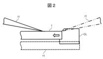
- the sample stage that holds the sample 1 with the backside raised includes, for example, a type that holds the outer periphery of the sample 1 with a clamp CL (see FIG. 2) and a type that holds the sample 1 with a pressure member while raising it with air pressure (for example, as disclosed in Japanese Patent Application Laid-Open No. 2017-504199, etc.).
- the rotating stage 12 is a stage that supports the sample stage 11.
- the rotating stage 12 also rotates about a vertical rotation axis (not shown), rotating the sample 1 together with the sample stage 11.
- the rotating stage 12 is equipped with an optically readable rotary encoder (not shown).
- the rotary encoder detects the rotation angle ( ⁇ coordinate) of the rotating stage 12 and outputs this information to the defect detection processing system 40.
- the detector for detecting the ⁇ coordinate is not limited to a rotary encoder, and any sensor that can detect the rotation angle with high accuracy can be used in place of the rotary encoder.
- the linear stage 13 is a stage that supports the rotating stage 12.
- the linear stage 13 moves along a rail (not shown) that extends in the radial direction (R-axis direction) of the rotating stage 12, and moves the sample 1 horizontally and linearly together with the rotating stage 12 and the sample stage 11.
- the linear stage 13 is equipped with an optically readable linear encoder (not shown).
- the linear encoder detects the position on the R-axis (R coordinate) of the linear stage 13 and outputs this information to the defect detection processing system 40.
- the detector for detecting the R coordinate is not limited to a linear encoder, and any sensor that can accurately detect a position on a straight line can be used in place of the linear encoder.
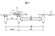
- FIG. 3 is a schematic diagram showing the movement path of the sample 1 inside the defect inspection device 100.
- a sample transfer position P1 and a scan start position P2 are set on the R axis, which is the linear track of the linear stage 13.
- a stage control circuit (not shown) in the defect detection processing system 40 is configured to drive the linear stage 13 to move the rotating stage 12 along a straight line including the sample transfer position P1 and the scan start position P2.
- the scan start position P2 is a position where the illumination light I1 is irradiated onto the sample 1 to start scanning the sample 1.
- the scan start position P2 is a position where a specific point of the sample 1 (center O in this embodiment (FIG.
- the other sample transfer position P1 is a position where the movement of the sample 1 to the scan start position P2 begins.
- the sample transfer position P1 also doubles as a position where the sample 1 is loaded and unloaded from the sample stage 11 by the transport arm Am (FIG. 3), for example. This sample transfer position P1 is away from the illumination light spot.
- the distance between the sample transfer position P1 and the scan start position P2 is about 150 mm to 500 mm.
- Position P3 indicates the position when the peripheral portion of the sample 1 is being scanned (sample peripheral portion scanning position).
- the illumination and detection unit 20 includes an illumination optical system 21 and a detection optical system 25.
- the illumination optical system 21 is an optical system that irradiates the sample 1 with illumination light I1, and includes an illumination light source (laser light source, etc.) 22 and a plurality of optical elements 23.
- the detection optical system 25 is an optical system that detects the inspection light I2 scattered or reflected by the sample 1, and includes a condensing optical element (condensing lens) 26, a photodetector 27, and a detection circuit 28. Since high inspection sensitivity is required, the illumination and detection unit 20 is close to the sample 1 (FIG. 3).
- the gap G between the sample stage 11 and the illumination and detection unit 20 is about several mm or less.
- the defect inspection device 100 of this embodiment is configured so that the distance between the illumination and detection unit 20 (the optical element at the lowest position) and the sample 1 is 0.5 mm to 5 mm or less in order to widely introduce the illumination light into the detector. Since it would be difficult to transport the sample 1 by the transport arm Am and insert it into this gap G to place it on the sample stage 11, a sample delivery position P1 is provided as shown in FIG.
- the illumination optical system 21 is installed on the opposite side of the scanning start position P2 from the sample transfer position P1. Therefore, the illumination light I1 is obliquely irradiated onto the sample 1 from the opposite side of the sample transfer position P1 (see FIG. 3).
- the oblique irradiation configuration is adopted in order to position the illumination optical system 21 to avoid the working space for loading and unloading the sample 1 and to reduce the distance between the sample transfer position P1 and the scanning start position P2.
- the illumination light source 22 is provided with a shutter (not shown) and is configured to irradiate the illumination light I1 onto the sample 1 or block the illumination light I1 by opening and closing the shutter.
- FIG. 4 is a plan view of a sample, which shows a schematic representation of the scanning trajectory of the sample by the defect inspection device 100.
- the shutter of the illumination light source 22 opens, the illumination light I1 emitted from the illumination light source 22 is irradiated onto the sample 1 via a plurality of optical elements 23.
- the illumination light I1 is irradiated along a spiral trajectory (scanning pitch: p0) from the center O of the sample 1 to its outer edge, as shown in FIG. 4, and the entire surface of the sample 1 is scanned.
- the inspection light I2 scattered or reflected by the sample 1 is detected via a focusing optical element (focusing lens) 26, a photodetector (e.g., a photoelectric sensor) 27, and a detection circuit 28.
- the detection circuit 28 outputs the detection result to a data processing circuit (not shown) in the defect detection processing system 40.
- the defect detection processing system 40 is programmed to drive the linear stage 13 from the scan start position P2 toward the illumination optical system 21 during defect inspection. That is, in this embodiment, the illumination optical system 21 is disposed on the opposite side of the sample transfer position P1. Therefore, during sample scanning, the movement of the linear stage 13 is controlled in a direction away from the sample transfer position P1, starting from the scan start position P2. As a result, even when a configuration is adopted in which the sample 1 is held by multiple clamps CL as the sample stage 11, as illustrated in FIG. 2, for example, it is possible to scan from the center O of the sample 1 to its outer edge while avoiding interference between the illumination light I1 and the clamps.
- FIG. 3 shows the case where the laser light is irradiated obliquely
- other light sources such as a broadband light source can also be used as the illumination light source 22, and the arrangement of the light source and the stage and the direction of irradiation from the light source to the sample can vary depending on the type of light source.
- the defect detection processing system 40 is equipped with an internal data processing circuit (not shown).
- the data processing circuit generates scan information (inspection results) from the detection results by the illumination and detection unit 20 and the R ⁇ coordinates output from the stage device 10.
- the scan information generated by the data processing circuit includes the positions of defects such as foreign matter and scratches, and the size and shape of the defects based on the amount of detection signals.
- the defect detection processing system 40 further includes a stage control circuit (not shown).
- the stage control circuit is a circuit that controls the operation of the stage device 10.
- the stage control circuit can be composed of, for example, a motor driver that drives the drive device (motor) of the rotating stage 12 and a motor driver that drives the drive device (motor) of the linear stage 13.
- the stage control circuit drives the drive device based on a command value for the operation of the stage device 10. This causes the rotating stage 12 and the linear stage 13 to operate.
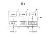
- FIG. 5 is a diagram showing an example of the hardware configuration of a defect detection processing system 40.
- the defect detection processing system 40 is a computer that controls the operation of the illumination detection unit 20, the rotation stage 12, and the linear stage 13 (stage device 10), etc.
- the defect detection processing system 40 includes, for example, an input interface 41, a ROM (e.g., an EPROM) 42, a RAM 43, a CPU 44, a timer 45, and an output interface 46, etc.
- a ROM e.g., an EPROM
- the input interface 41 transfers to the CPU 44 signals from the encoders of the rotary stage 12 and the linear stage 13 (R and ⁇ coordinates of the sample stage 11) and inspection conditions input from an input device such as a keyboard (not shown) in response to the operator's operation.
- the inspection conditions include, for example, the type, size, shape, etc. of the sample 1 and information on the inspection mode.
- the ROM 42 stores the calculation formulas, programs (described later), and data required for defect inspection.
- the RAM 43 stores numerical values during calculations and information such as inspection conditions input from the input device.
- the output interface 46 outputs command signals to the stage device 10 and the illumination detection unit 20 in response to commands from the CPU 44.
- the defect detection processing system 40 also outputs coordinate detection signals of the rotary stage 12 and the linear stage 13 (calculated R and ⁇ coordinates of the sample stage 11) to a data processing circuit (not shown) via the output interface 46.
- the CPU 44 executes a predetermined process based on the information input via the input interface 41, in accordance with the program loaded from the ROM 42.
- the stage device 10 and the illumination detection unit 20 are also controlled by command values output from the CPU 44 based on the inspection conditions and the R ⁇ coordinate of the sample stage 11 to be measured, and the sample 1 is scanned in this way.
- the defect inspection apparatus 100 can operate in a number of inspection modes, including a constant angular velocity (CAV) inspection, a constant linear velocity (CLV) inspection, and an acceleration/deceleration inspection.
- CAV inspection is an inspection mode in which the rotational speed (angular velocity) of the rotating stage 12 during scanning is kept constant.
- CLV inspection is an inspection mode in which the linear velocity (scanning speed) is kept constant.
- Acceleration/deceleration inspection is an inspection mode in which inspection is performed even during acceleration and deceleration. "During acceleration” means that the inspection does not begin once the specified stage rotation speed is reached, but rather begins during the acceleration process leading up to the specified stage rotation speed. "During deceleration” means that while the inspection normally ends at the specified stage rotation speed and then the stage rotation decelerates and stops, the inspection continues partway through the deceleration process of the rotation speed and ends during deceleration.
- the acceleration/deceleration inspection mode will be described in detail.
- the stage device 10 with large inertia it takes more time to increase the rotation speed of the stopped stage to the specified rotation speed (or to stop the sample stage rotating at the specified rotation speed) than to move linearly between the sample delivery position P1 and the scan start position P2. Therefore, when the sample stage 11 moves linearly from the sample delivery position P1 and arrives at the scan start position P2, the stage rotation speed does not reach the specified rotation speed. If the specified rotation speed is increased in response to a user request, the time required for rotation acceleration/deceleration will be extended. On the other hand, if the moving distance is shortened, the moving time will be shortened.
- the time difference between the time required for rotation acceleration/deceleration and the time required for stage movement will become wider. If scanning is started with the stage rotating at the specified rotation speed as usual, there will be a time to wait for the specified rotation speed to be reached at the scan start position P2. When returning the sample stage 11 to the sample delivery position P1 after scanning, there may also be a time to wait for the sample stage 11 to stop rotating at the sample delivery position P1. If the specified rotation speed increases and the travel distance decreases, the overall inspection processing time can be reduced by shortening the scanning time and travel time, but on the other hand, the proportion of waiting time in the inspection processing time increases due to the increased time difference between the time required for rotation acceleration and the time required for travel.
- the net irradiation time can be maximized within the specified sequence by devising controls over the linear velocity and angular velocity of the stage (described later).
- the defect inspection device 100 can use different inspection modes, such as CAV inspection, CLV inspection, or acceleration/deceleration inspection, depending on the user's application and needs. However, because the defect inspection device 100 has different inspection modes, control corresponding to each inspection mode is required in controlling the illumination detection unit 20 and the stage device 10, making the control method complicated.
- FIG. 6 is a schematic diagram for explaining optical vibration and mechanical vibration in the defect inspection device 100.
- the optical vibration is caused by the fluctuation of the illumination light I1 of the illumination optical system 21.
- the fluctuation of the illumination light I1 is caused by the vibration of the optical element 23 (the mechanical vibration of the stage device 10 is also a factor), the vibration of the air, and/or the external environment (temperature and humidity).
- the mechanical vibration is caused by the vibration applied to the rotation stage 12 and the linear (translation) stage 13 of the stage device 10.
- the detection optical system 25 detects the inspection light I2 scattered or reflected by the sample 1.
- the defect detection processing system 40 calculates the defect coordinates based on the detection signal and the R ⁇ coordinates output from the stage device 10. At this time, correction is required to take into account the amount of deviation in coordinate information caused by optical vibrations and mechanical vibrations relative to the coordinates where the defect actually exists. Note that while conventionally attempts have been made to eliminate the effects of vibration using only the vibration isolation mount 14, this embodiment measures the amount of positional deviation caused by vibrations (fine vibrations) that cannot be completely eliminated by the vibration isolation mount 14, and reflects this amount of positional deviation in the measured defect coordinates based on signal processing.
- the light beam position sensor 50 is installed on the illumination optical path from the illumination light source 22 to the sample 1 (on an extension of a part of the illumination optical path). It is preferable to install the light beam position sensor 50 as late as possible in the illumination optical path. This is because it is difficult to accurately obtain positional deviation caused by vibration of the optical element 23 and the like downstream of the light beam position sensor. In addition, it is necessary to adjust the position of the light irradiated to the light beam position sensor 50 so that it is at the center of the light beam position sensor 50.
- a reflective or transmissive optical element is placed on the irradiation optical path, and the optical path is adjusted so that the inspection light is near the center of the light beam position sensor 50 by the optical element.
- the beam should enter the center of the light beam position sensor 50, but the beam inevitably wobbles as it travels along the optical path. Therefore, the illumination light I11 entering the light beam position sensor 50 during actual inspection is incident slightly off the center point.
- the light beam position sensor 50 detects the actual incident position.
- the difference between the actual incident position when the center point is set as the reference position can be the "position deviation amount" output by the light beam position sensor 50.
- a part of the light may be extracted by a beam splitter and made to enter the light beam position sensor 50.
- the light beam position sensor 50 must be capable of measuring the deviation amount of both the angle and position of the illumination light I1, or at least two sensors capable of measuring the position deviation must be installed on the optical path. This allows the position of the laser beam to be measured at all times. When two sensors are installed, the angle of the laser beam can be calculated from the positions of the laser beam detected by each sensor.
- a displacement sensor 60 is mounted on the stage device 10, for example, on the linear stage 13, on a vibration isolation mount 14.
- An acceleration sensor 70 is mounted on the rotation stage 12 and measures the amount of positional deviation in the R-axis and ⁇ -axis directions.
- the vibration isolation mount 14 structurally reduces disturbance vibrations from other units outside and inside the device (it directly attenuates vibrations as a physical quantity (not by data processing)).
- the displacement sensor 60 detects low-frequency external vibrations that cannot be removed by the vibration isolation mount 14. Examples of external vibrations include vibrations from the floor of a factory in which the defect inspection device 100 is installed, vibrations caused by the influence of vibrations from nearby devices, and vibrations caused by fans within the device.
- the acceleration sensor 70 detects high-frequency vibrations such as vibrations caused by the rotational movement of the rotating stage 12, vibrations caused by accelerating or decelerating the rotation, and vibrations caused by imbalance of the rotating body.
- the displacement sensor 60 is highly sensitive to low-frequency vibrations
- the acceleration sensor 70 is highly sensitive to vibration measurements in the high-frequency range. The sum of the displacement amounts due to low-frequency and high-frequency vibrations output by these sensors can be taken as the "position deviation amount" due to mechanical vibration.
- the optical vibrations caused by the fluctuations of the illumination light I1 are detected by the light beam position sensor 50, and the mechanical vibrations caused by the fluctuations on the stage device 10 side are detected by the displacement sensor 60 and the acceleration sensor 70.
- FIG. 7 is a flowchart for explaining the process executed by the defect detection processing system 40. As shown in FIG.
- the defect detection processing system 40 detects defects from the inspection light I2 signal detected via the photodetector (e.g., photoelectric sensor) 27 and the detection circuit 28, and the stage encoder signal detected by the rotation stage encoder (not shown) and the translation stage encoder (not shown), and calculates the coordinates of the defects.
- the calculated coordinates include components of positional deviation due to the above-mentioned optical vibration and mechanical vibration.
- the defect detection processing system 40 calculates the amount of positional deviation of the illumination light I 12 irradiated onto the sample 1 from the amount of positional deviation of the illumination light I 11 detected by the light beam position sensor 50 .
- the distance from the illumination light source 22 to the light beam position sensor 50 and the distance from the illumination light source 22 to the sample 1 may differ. Therefore, the amount of positional deviation of the illumination light I11 detected by the light beam position sensor 50 differs from the amount of positional deviation of the illumination light I12 on the sample 1. Therefore, in this embodiment, the relative relationship between the amount of positional deviation of the light beam position sensor 50 and the amount of positional deviation on the sample 1 is obtained by measurement in advance, and stored in a storage device (not shown) in the defect detection processing system 40 (for example, as a table).
- the defect detection processing system 40 may obtain the amount of positional deviation of the illumination light I12 corresponding to the amount of positional deviation of the illumination light I11 detected by the light beam position sensor 50 from the storage device. A detailed example of the calculation of the optical positional deviation will be described later.
- the defect detection processing system 40 calculates the amount of positional deviation caused by mechanical vibration by adding together (vector sum) the amount of displacement caused by low-frequency vibration detected by the displacement sensor 60 installed on the stage device 10 on the vibration isolation mount 14 and the amount of displacement caused by high-frequency vibration detected by the acceleration sensor 70 of the rotation stage 12. A detailed example of the calculation of the amount of mechanical positional deviation will be described later.
- the defect detection processing system 40 calculates the coordinate correction amount by vector addition of the positional deviation amount due to optical vibration obtained in S702 and the positional deviation amount due to mechanical vibration obtained in S703.
- the defect detection processing system 40 reflects the coordinate correction amount calculated in S704 to the coordinates calculated in S701, and outputs the presence or absence of a defect in the sample 1 and the coordinate value (correction value) of the defect.
- Fig. 8 is a diagram showing an example of a defect coordinate shift on a wafer.
- the illumination light I12 is irradiated onto the sample 1 on the sample stage 11 on the rotary stage 12 via a plurality of optical elements 23.
- the illumination light I12 is first irradiated onto the center position O of the sample 1.
- the illumination light is irradiated in a spiral shape from the center to the periphery as shown in FIG. 8.
- This trajectory may be a spiral trajectory in which the illumination light is irradiated in sequence from the periphery to the center.
- the light irradiated onto the sample 1 vibrates due to vibrations associated with the optical elements 23 on the optical path, changes in temperature and humidity around the illumination optical system 21 in the device, and the like. This causes the irradiation position to shift from the scanning trajectory that should be irradiated by the illumination light. This affects the defect coordinates to be output, reducing the accuracy of the defect coordinates.
- a defect inspection device 100 that has multiple different inspection modes, there are factors that make the correction of the positional deviation due to this vibration even more complicated. For example, if the inspection mode (CAV inspection mode, CLV inspection mode, acceleration/deceleration inspection mode, etc.) differs, the rotation speed of the rotating stage 12 and the movement feed pitch of the linear stage also differ. Furthermore, there are also inspection modes in which the rotation speed and feed pitch change during one inspection. For this reason, the manner in which vibration occurs and the magnitude and change of the resulting positional deviation are completely different depending on the inspection mode.
- a reference model for each sensor output is provided in advance for each inspection mode.
- Fig. 11B and Fig. 11C are diagrams showing a comparison between a reference model (shown by a dotted line in the figure) and the output of the displacement sensor 60 and the acceleration sensor 70 (shown by a solid line in the figure) in an acceleration/deceleration inspection mode, which is one of the inspection modes (inspection conditions).
- the reference model of displacement and acceleration is a model that represents an ideal form of how the displacement and acceleration of the rotation stage 12 should be from the start to the end of the inspection.
- Fig. 11B and Fig. 11C plot the acceleration (actual measurement value) actually detected by the displacement sensor 60 and the acceleration sensor 70 attached to the rotation stage 12.
- This actually measured acceleration includes the effect of the actual displacement amount of the vibration isolation mount 14 and the mechanical vibration caused by the acceleration of the rotation stage 12. Therefore, a difference occurs between the detection values of the displacement sensor 60 and the acceleration sensor 70 for the displacement model and the acceleration model.
- the rotation speed accelerates in the beginning of an inspection, rotates at a constant speed in the middle, and decelerates near the end of the inspection (see FIG. 11A). Therefore, the reference values of the displacement model and acceleration model are different in the beginning, middle, and near the end of an inspection.
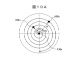
- defects a, b, and c are located at different radial distances from the center to the periphery as shown in FIG. 10A.
- defect a near the center is inspected while the rotating stage is accelerating
- defect b is inspected while the rotating stage is rotating at a constant speed
- defect c is inspected while the rotating stage is decelerating.
- the difference between the displacement and acceleration output by the displacement/acceleration sensor when each defect is detected and the displacement/acceleration model is the positional deviation amount that affects the defect coordinates.
- ⁇ X represents the X-direction component of the positional deviation due to optical vibration
- ⁇ Y represents the Y-direction component of the positional deviation due to optical vibration
- ⁇ X represents the X-direction component of the positional deviation due to mechanical vibration
- ⁇ Y represents the Y-direction component of the positional deviation due to mechanical vibration
- More accurate coordinates can be obtained by measuring the positional deviation ( ⁇ , ⁇ ), calculating the correction amount, and correcting the coordinate information of the conventional inspection results. In this way, the defect detection processing system 40 calculates the coordinate correction amount (vector amount) and corrects the defect coordinates accordingly.
- Figures 9A and 9B are diagrams for explaining a specific example of correction of the deviation amount of defect coordinates due to optical vibration.
- Figure 9A is a diagram showing an example of an illumination light spot S10 irradiated on the sample 1 and a trajectory of a scanning line.
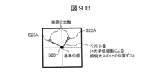
- Figure 9B is a diagram showing an example of a trajectory of an illumination light spot S20 on a light beam position sensor 50.
- S11, S12, and S13 show hypothetical illumination light spots when ideal scanning is performed when there is no effect of optical vibrations, and when the rotation stage 12 and the linear stage 13 are not affected by mechanical vibrations and are ideally controlled (in reality, optical and mechanical vibrations always occur in the process of irradiating the sample with illumination light).
- the illumination light spot S10 (scanning start point (inner circumference of the sample)) scans in a spiral trajectory along the scanning line as shown by S11, S12, and S13 in an ideal state without vibration. Also, as shown in Figure 9B, in a state without any vibration, the illumination light spot S20 irradiated onto the sensor surface of the light beam position sensor 50 is at the reference position.
- the illumination light spot S11 vibrates, and the illumination light spot S12 is scanned as S12A, and the illumination spot S13 is scanned as S13A, shifting its position from the scanning line.
- the illumination light spot S20 on the light beam position sensor 50 shown in FIG. 9B also shifts from the reference position as S22A and S23A.
- the illumination light spots S20, S22A, and S23A of the light beam position sensor 50 are correlated with the positions of the illumination light spots S10, S11, S12, and S13 irradiated onto the sample 1. This correlation is determined in advance by simulation, actual measurement, or the like. The difference between the beam position detected by the light beam position sensor 50 and a reference is determined as the amount of deviation in the light beam position sensor. Then, the amount of positional deviation of the illumination light spots irradiated onto the sample 1 is calculated from this amount of deviation and the correlation determined in advance.
- the defect detection processing system 40 performs this series of processes and reflects the amount of deviation due to optical vibration in the defect coordinates. This is coordinate correction for the amount of deviation due to optical vibration.
- FIGS. 10A and 10B are diagrams for explaining a specific example of correction of deviation amount of defect coordinates due to mechanical vibration.
- Figure 10A is a diagram showing an example of the position of a defect when there is no mechanical vibration.
- Figure 10B is a diagram showing an example of the position of a defect when there is mechanical vibration.
- the defect coordinates are calculated based on the rotation angle ( ⁇ coordinate) and the position on the R axis (R coordinate) obtained from various encoders.
- ⁇ coordinate the position on the R axis
- R coordinate the position on the R axis obtained from various encoders.
- FIG. 10A the coordinates of defects a, b, and c without mechanical vibration are shown.
- mechanical vibration occurs due to the rotation or linear stage.
- the center position of the sample held on the sample stage 11 is shifted (O ⁇ O1).
- the rotation angle and the position on the R axis are shifted from the center position of the sample 1 (O: the center position of the illumination light spot when there is no mechanical vibration) to the original defect coordinates on the sample 1 (O1: the center position of the illumination light spot when there is mechanical vibration).
- the defect coordinates calculated based on the rotation angle ( ⁇ coordinate) and the position on the R axis (R coordinate) obtained from various encoders are shifted from the original coordinates.
- the defect detection processing system 40 uses the difference (deviation amount) between the reference model and the actual output of the displacement sensor 60 and the acceleration sensor 70 to correct the deviation amount.
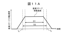
- FIG. 11A shows the speed change of the linear stage during CAV scanning.
- FIG. 11B shows the output change of the acceleration sensor 70 (in one axial direction) during CAV scanning.
- FIG. 11C shows the output change of the displacement sensor 60 (in one axial direction) during CAV scanning.
- the dotted line shows the reference model which is an ideal output in the absence of mechanical vibration.
- D1 represents an inspection mode in which inspection is performed during constant speed rotation of the rotating stage 12 (i.e., no inspection is performed during acceleration or deceleration).
- D2 represents an inspection mode in which inspection is performed even during acceleration or deceleration of the rotating stage 12.
- t S represents the measurement start timing (time).
- the time until t S represents the time period during which the sample 1 is transported from the sample delivery position P1 to the scan start position P2.
- t E represents the measurement end timing (time).
- the time from tE indicates the time period during which the sample 1 is transported from the scanning end position to the sample delivery position P1.
- the acceleration increases during acceleration/deceleration and becomes zero during uniform motion.
- the low-frequency vibration value is linked to the rotation angle ( ⁇ coordinate) of the rotating stage 12 and the linear stage 13 and the position on the R axis (R coordinate).
- the measurement data by the accelerometer is also linked to the rotation angle ( ⁇ coordinate) and the position on the R axis (R coordinate).
- a defect inspection apparatus (defect inspection system) 100 comprises an illumination detection unit 20 having an illumination light source 22 for irradiating light (laser light) onto the sample 1 and a detection circuit (detector) 28 for detecting the inspection light from the sample 1, a stage device (stage mechanism) 10 which holds the sample 1 and has a linear stage 13 and a rotational stage 12, a displacement sensor (position sensor) 60 which measures the positions of the linear stage 13 and the rotational stage 12, and an acceleration sensor (accelerometer) 70 which measures vibrations of the linear stage 13 and the rotational stage 12, and a defect detection processing system (control unit) 40 which determines defect coordinates indicating the position of a defect on the sample 1 based on the measurement values by the displacement sensor 60.
- an illumination detection unit 20 having an illumination light source 22 for irradiating light (laser light) onto the sample 1 and a detection circuit (detector) 28 for detecting the inspection light from the sample 1, a stage device (stage mechanism) 10 which holds the sample 1 and has a linear stage
- the defect detection processing system 40 compares an output reference model (see FIG. 11B) of the acceleration sensor 70 calculated in advance according to an inspection mode (inspection conditions) that specifies the inspection method of the sample 1 with a value actually measured by the acceleration sensor 70 during inspection of the sample 1 according to the inspection mode to determine a mechanical positional deviation amount in the stage device 10, and corrects the defect coordinates using the mechanical positional deviation amount.
- the output reference model is a characteristic that indicates an output value of the acceleration sensor 70 when there is no mechanical vibration of the linear stage 13 and the rotation stage 12 (see FIG. 11B).
- the inspection mode includes at least one of the following: a CAV inspection mode, which is an inspection method in which the rotation speed of the rotating stage is constant; a CLV inspection mode, which is an inspection method in which the scanning speed of light (illumination light) is constant; and an acceleration/deceleration inspection mode in which inspection is performed even while the linear stage 13 is accelerating and decelerating.
- the inspection mode may be configured so that the operator can select it as appropriate, or may be configured to be set in advance.
- the defect detection processing system 40 corrects the defect coordinates based on the output reference model corresponding to the set inspection mode.
- the defect inspection system 100 performs positional deviation correction due to optical vibration in addition to positional deviation correction due to mechanical vibration.
- the illumination detection unit 20 includes a light beam position sensor (light position sensor) 50 that detects the amount of optical displacement from the irradiation reference position of light from the illumination light source 22.
- the defect detection processing system 40 corrects the amount of optical positional deviation included in the defect coordinates based on the amount of optical displacement detected by the light beam position sensor 50. No matter what illumination light source is used, a deviation in the irradiation position will occur. In conventional defect inspections, such a deviation in the irradiation position of the illumination light did not have much effect on defect position detection.
- the deviation in position due to optical vibration fluctuation of illumination light
- the light beam position sensor 50 is installed on an extension of a part of the optical path from the illumination light source 22 to the sample 1. However, the installation position of the light beam position sensor 50 does not coincide with the light irradiation position on the sample 1.
- the defect detection processing system 40 obtains the light irradiation position deviation amount corresponding to the optical displacement amount actually detected by the light beam position sensor 50 from the storage device, and adds the light irradiation position deviation amount to the defect coordinates to correct the optical position deviation amount. In this way, it is possible to accurately correct the position deviation due to optical vibration.
- the defect inspection system 100 includes a means for correcting the positional deviation caused by optical vibration by signal processing, and a means for correcting the positional deviation caused by mechanical vibration by signal processing.
- the defect detection processing system 40 corrects the positional deviation caused by the optical vibration of the illumination optical system and the positional deviation caused by the mechanical vibration of the stage mechanism in the defect coordinates using the optical displacement amount detected by the light beam position sensor 50 and the measurement values by the displacement sensor (position sensor) 60 and the acceleration sensor (accelerometer) 70.
- the positional deviation correction is a process different from the mechanism for preventing the occurrence of positional deviation by the vibration isolation mount 14 for reducing disturbance vibration from outside the defect inspection system 100 and disturbance vibration inside the defect inspection system 100.
- the positional deviation amount due to the mechanical vibration in the stage device 10 is a vibration of a lower frequency than the disturbance vibration, and includes a positional deviation amount due to vibration that is not removed by the vibration isolation mount 14.
- the positional deviation correction according to this embodiment is not a mechanism that physically prevents the occurrence of positional deviation, as in the case of positional deviation removal by the vibration isolation mount 14 (the vibration isolation mount 14 structurally attenuates disturbance vibrations), but rather a process that detects the amount of optical positional deviation (vector value) and the amount of mechanical positional deviation (vector value) as signals and corrects these positional deviation amounts by digital signal processing (adding the vector value corresponding to the positional deviation to the defect coordinates). In this way, positional deviation due to low-frequency vibrations can be efficiently corrected by signal processing, and highly accurate information on the defect position can be output.
- the defect detection processing system 40 also uses signal processing to correct the amount of positional deviation caused by high-frequency vibration resulting from the rotational movement of the rotating stage as the amount of positional deviation caused by mechanical vibration. This makes it possible to accurately remove the effects of minute vibrations that cannot be removed by the vibration isolation mount 14.
- the functions of this embodiment can also be realized by software program code.
- a storage medium on which the program code is recorded is provided to a system or device, and the computer (or CPU or MPU) of that system or device reads the program code stored in the storage medium.
- the program code itself read from the storage medium realizes the functions of the above-mentioned embodiment, and the program code itself and the storage medium on which it is stored constitute this disclosure.
- Examples of storage media for supplying such program code include flexible disks, CD-ROMs, DVD-ROMs, hard disks, optical disks, magneto-optical disks, CD-Rs, magnetic tapes, non-volatile memory cards, and ROMs.
- an operating system (OS) running on a computer may perform all or part of the actual processing based on the instructions of the program code, and the functions of the above-mentioned embodiments may be realized by this processing.
- OS operating system
- a CPU of the computer may perform all or part of the actual processing based on the instructions of the program code, and the functions of the above-mentioned embodiments may be realized by this processing.
- the program code of the software that realizes the functions of the embodiment may be distributed over a network and stored in a storage means such as a hard disk or memory of the system or device, or in a storage medium such as a CD-RW or CD-R, so that when used, the computer (or CPU or MPU) of the system or device reads out and executes the program code stored in the storage means or storage medium.
- a storage means such as a hard disk or memory of the system or device
- a storage medium such as a CD-RW or CD-R
- the technology disclosed herein is not limited to the configuration example of this embodiment, but includes various modified examples. This embodiment is provided to clearly explain the technology disclosed herein. Therefore, the technology disclosed herein is not necessarily limited to having all of the configurations described. Furthermore, the processes and techniques described in this embodiment are not inherently related to any specific device, and can be implemented by combining each component. Furthermore, various types of general-purpose devices can also be added. A dedicated device may be constructed to perform the functions of this embodiment. Furthermore, various functions can be formed by appropriately combining multiple components disclosed in this embodiment. For example, some components may be deleted from all the components shown in the embodiment, or different components may be appropriately combined.
- control lines and information lines are those that are considered necessary for the explanation, and not all control lines and information lines in the product are necessarily shown. All components may be interconnected.
Landscapes
- Investigating Materials By The Use Of Optical Means Adapted For Particular Applications (AREA)
Abstract
本開示は、様々な検査モード(検査条件)で欠陥検査している状態であっても振動による位置ずれを正確に補正するため、(i)試料に光を照射する光源と、試料からの光を検出する検出器と、を有する照明検出ユニットと、(ii)試料を保持し、直進ステージおよび回転ステージと、直進ステージおよび前記回転ステージの位置を計る位置センサと、直進ステージおよび回転ステージの振動を計るための加速度計と、を有するステージ機構と、(iii)位置センサによる計測値に基づいて、欠陥の位置を示す欠陥座標を求める制御部と、を備え、(iv)制御部は、試料の検査方法を規定する検査モードに応じて予め計算された加速度計の出力基準モデルと、検査モードに従って試料の検査中に加速度計で実測された値とを比較してステージ機構における機械的位置ずれ量を求め、当該機械的位置ずれ量を用いて欠陥座標を補正する、欠陥検査システムを提案する(図6参照)。
Description
本開示は、欠陥検査システムに関する。
半導体製造工程では、試料の欠陥(傷や異物等)が歩留りに与える影響が大きく、欠陥検査装置による欠陥検査情報を半導体製造工程及び製造装置にフィードバックすることが歩留り管理には重要である。このため、ウェーハ等の試料をインライン検査する欠陥検査装置が半導体製造工程において果たす役割は大きい。
欠陥検査に関し、例えば、特許文献1は、主走査である回転移動θと副走査である直進(並進)移動Rを組み合わせ、照明スポット(照明光の照射位置)を半導体ウェーハの表面上で螺旋状に走査して欠陥を検出する欠陥検査装置を開示する。また、特許文献1は、欠陥検査装置が、CAV(Constant Angular Velocity)走査、CLV(Constant Linear Velocity)走査による欠陥検査モード、及び試料ステージの回転加速あるいは減速中にも検査する加減速検査等、複数の異なる検査モードで動作することを開示している。各検査モードでは、半導体ウェーハ等の円形試料を内周から外周、または外周から内周へと回転走査して検査する過程の異なる半径距離の領域において、1検査点あたりの照射速度とそれに伴う照射量が変化する。
欠陥検査装置は、検査感度およびスループットの向上が常に求められている。しかし、感度とスループットはトレードオフの関係にある。特許文献1が開示する加減速検査は、それまで検査をしていなかった時間であって、ステージが一定速度まで加速又は減速している最中の時間の一部を検査時間として活用することにより、トータル検査時間を短縮するモードである。従って、スループット向上には非常に有用な手段となっている。
その一方で、上記加減速検査モードは、制御が難しいという側面がある。これは、ステージを一定速度で回転させてから試料を検査する場合に比べ、加速中又は減速中の検査において、試料に照射する照明ビーム、ステージ、および装置全体に係る振動が複雑となるためである。特に、特許文献1に記載のCAV(Constant Angular Velocity)走査、CLV(Constant Linear Velocity)走査といった複数の検査モードを用いる欠陥検査装置では、モードに応じて振動の傾向が変わってくる。
ところが、特許文献1に開示するような技術においては、異なる検査モードにより生じる振動の影響に対する対策を講じることが望ましい。このような振動は、欠陥検査装置が出力する欠陥座標精度に影響する。特に、試料が半導体ウェーハである場合、半導体パターンの微細化に伴い検出したい欠陥サイズも小さくなっている。欠陥像の確認は、欠陥検査装置が欠陥の有無とその座標を出力し、レビューSEMでその座標に基づいて確認される。その際、欠陥検査装置が出力した欠陥座標にずれがあると、レビューSEMで当該欠陥を見つける際、時間が掛かってしまい、スループットの向上が図れない。特に、確認したい欠陥サイズが小さければ小さいほど、わずかな座標ずれにより、後のレビューSEMにおける観察の際の欠陥位置の特定が困難になってしまう。このように、欠陥検査装置内の様々な振動によって生じる座標ずれも半導体分野では許容されにくくなってきている。そのため、複数の検査モードを使い分けても、出力する欠陥座標を正しく補正できる手段が求められる。
本開示は、このような状況に鑑み、様々な検査モード(検査条件)で欠陥検査している状態であっても振動による位置ずれを正確に補正する技術を提案する。
上記課題を解決するために、本開示は、試料の欠陥を検査する欠陥検査システムであって、(i)試料に光を照射する光源と、試料からの光を検出する検出器と、を有する照明検出ユニットと、(ii)試料を保持し、直進ステージおよび回転ステージと、直進ステージおよび前記回転ステージの位置を計る位置センサと、直進ステージおよび回転ステージの振動を計るための加速度計と、を有するステージ機構と、(iii)位置センサによる計測値に基づいて、欠陥の位置を示す欠陥座標を求める制御部と、を備え、(iv)制御部は、試料の検査方法を規定する検査モードに応じて予め計算された加速度計の出力基準モデルと、検査モードに従って試料の検査中に加速度計で実測された値とを比較してステージ機構における機械的位置ずれ量を求め、当該機械的位置ずれ量を用いて欠陥座標を補正する、欠陥検査システムを提供する。
本開示に関連する更なる特徴は、本明細書の記述、添付図面から明らかになるものである。また、本開示の態様は、要素及び多様な要素の組み合わせ及び以降の詳細な記述と添付される請求の範囲の様態により達成され実現される。
本明細書の記述は典型的な例示に過ぎず、本開示の請求の範囲又は適用例を如何なる意味においても限定するものではない。
本明細書の記述は典型的な例示に過ぎず、本開示の請求の範囲又は適用例を如何なる意味においても限定するものではない。
本開示の技術によれば、様々な検査モード(検査条件)で欠陥検査している状態であっても振動による位置ずれを正確に補正することができる。
本開示の実施形態は、ウェーハ等の試料の欠陥を検査する欠陥検査システムに関する。本実施形態は、欠陥検査システムにおいて、検査モード(CAV、CLV、加減速検査モードなど)が異なったとしても、試料を載置するステージなどの振動に起因する機械的振動および照明系におけるレーザ光の揺らぎなどに起因する光学的振動の両者を考慮して欠陥座標のずれ量を補正する技術を開示する。
以下、添付図面を参照して本開示の実施形態について詳細に説明する。添付図面では、機能的に同じ要素は同じ番号で表示される場合もある。なお、添付図面は本開示の原理に則った具体的な実施形態と実装例を示しているが、これらは本開示の理解のためのものであり、決して本開示を限定的に解釈するために用いられるものではない。
また、本実施形態では、当業者が本開示を実施するのに十分詳細にその説明がなされているが、他の実装・形態も可能で、本開示の技術的思想の範囲と精神を逸脱することなく構成・構造の変更や多様な要素の置き換えが可能であることを理解する必要がある。従って、以降の記述をこれに限定して解釈してはならない。
<欠陥検査装置の構成例>
ここでは、欠陥検査装置(欠陥検査システム)100の基本的構成について説明する。説明を単純にするため、まずは機械的および光学的振動補正機能を除いた部分の構成について説明する。
ここでは、欠陥検査装置(欠陥検査システム)100の基本的構成について説明する。説明を単純にするため、まずは機械的および光学的振動補正機能を除いた部分の構成について説明する。
図1は、欠陥検査装置100の基本的構成例を示す図である。図1に示す欠陥検査装置100は、回転しながら直進移動する試料1に照明光I1を照射し、螺旋状又は同心円状に試料1を走査して試料1の欠陥を検査する方式である。試料1としては、例えばウェーハ(ベアウェーハ、膜付きウェーハ、パターン付きウェーハ等の半導体製造プロセスの各段階のウェーハを含む)のような円形板状のものを想定することができる。ただし、ウェーハ以外の半導体用デバイス基板でも良く、試料1はウェーハに限定するものではない。また、検査により検出する欠陥は、試料1の傷やうねり、試料1に付着した異物等が該当する。
欠陥検査装置100は、基本的構成として、ステージ装置10と、照明検出ユニット20と、除震マウント14と、データ処理回路(不図示)およびステージ制御回路(不図示)を内部に含む欠陥検出処理システム40と、を備えている。これら要素について順次説明する。
(i)ステージ装置
ステージ装置10は、回転運動と直進(並進)運動の機能を備えた回転直進ステージである。当該ステージ装置10は、試料ステージ11と、回転ステージ12と、直進ステージ13とを含んでいる。また、ステージ装置10は、照明検出ユニット20とともに、装置外部および内部の他ユニットからの外乱振動を低減させるための除震マウント14上に設置されている。
ステージ装置10は、回転運動と直進(並進)運動の機能を備えた回転直進ステージである。当該ステージ装置10は、試料ステージ11と、回転ステージ12と、直進ステージ13とを含んでいる。また、ステージ装置10は、照明検出ユニット20とともに、装置外部および内部の他ユニットからの外乱振動を低減させるための除震マウント14上に設置されている。
試料ステージ11は、ウェーハ等の試料1を水平に保持するステージである。試料ステージ11には、試料1の裏面を吸着して試料1を保持するもの(例えば、特開平11-233597号公報等に開示)の他、試料のエッジをグリップする等して裏面を浮かせた状態で試料1を保持するもの等、種々の方式のものが採用され得る。試料1の裏面を吸着する試料ステージは、例えば、半導体デバイスメーカで欠陥検査装置100を使用する場合に用いられる。裏面を浮かせて試料1を保持する試料ステージは、例えば、試料1の裏面を試料ステージに接触させることが許容されないウェーハメーカで欠陥検査装置100を使用する場合に用いられる。裏面を浮かせて試料1を保持する試料ステージには、例えば試料1の外周をクランプCLで保持する方式(図2参照)や、試料1を空圧で浮かせつつ押え部材で保持する方式(例えば、特表2017-504199号公報等に開示)がある。
回転ステージ12は、試料ステージ11を支持するステージである。また、回転ステージ12は、鉛直な回転軸(不図示)を中心にして自転し、試料ステージ11と共に試料1を回転させる。回転ステージ12は、光学読み取り式のロータリエンコーダ(不図示)を備える。当該ロータリエンコーダは、回転ステージ12の回転角度(θ座標)を検出し、その情報を欠陥検出処理システム40に出力する。但し、θ座標を検出するための検出器は、ロータリエンコーダには限定されず、精度良く回転角度が検出できるセンサであればロータリエンコーダに代えて採用することができる。
直進ステージ13は、回転ステージ12を支持するステージである。直進ステージ13は、回転ステージ12の半径方向(R軸方向)に延びるレール(不図示)に沿って移動し、回転ステージ12及び試料ステージ11と共に試料1を水平方向に直線的に移動させる。直進ステージ13は、光学読み取り式のリニアエンコーダ(不図示)を備える。当該リニアエンコーダは、直進ステージ13のR軸上の位置(R座標)を検出し、その情報を欠陥検出処理システム40に出力する。ただし、R座標を検出するための検出器は、リニアエンコーダには限定されず、精度良く直線上の位置が検出できるセンサであればリニアエンコーダに代えて採用することができる。
図3は、欠陥検査装置100の内部における試料1の移動経路を示す模式図である。本実施形態においては、図3に示すように、直進ステージ13の直線軌道であるR軸上に試料受渡し位置P1と走査開始位置P2が設定されている。欠陥検出処理システム40内のステージ制御回路(不図示)は、直進ステージ13を駆動することで、試料受渡し位置P1及び走査開始位置P2を含む直線に沿って回転ステージ12を移動させることができるように構成されている。走査開始位置P2とは、試料1に照明光I1を照射して試料1の走査を開始する位置である。具体的には、走査開始位置P2は、照明検出ユニット20の照明光スポット(照明光I1の焦点位置)に試料1の特定点(本実施形態では中心O(図4))が一致する位置である。他方の試料受渡し位置P1は、走査開始位置P2への試料1の移動を開始する位置である。また、試料受渡し位置P1は、例えば、試料ステージ11に対して搬送アームAm(図3)により試料1を脱着(ロード及びアンロード)する位置を兼ねている。この試料受渡し位置P1は、照明光スポットから離れている。本実施形態では、試料受渡し位置P1と走査開始位置P2との距離は150mmから500mm程度である。なお、位置P3は、試料1の周縁部を走査しているときの位置を示している(試料周縁部走査位置)。
(ii)照明検出ユニット
照明検出ユニット20は、照明光学系21と、検出光学系25と、を備える。照明光学系21は、照明光I1を試料1に照射する光学系であり、照明光源(レーザ光源等)22と、複数の光学素子23と、を含んで構成される。検出光学系25は、試料1で散乱又は反射した検査光I2を検出する光学系であり、集光光学素子(集光レンズ)26と、光検出器27と、検出回路28と、を含んで構成される。なお、高い検査感度が要求されることから照明検出ユニット20は、試料1に接近している(図3)。試料ステージ11が照明検出ユニット20の直下にあるとき、試料ステージ11と照明検出ユニット20との間隙Gは、数mm程度かそれ以下である。本実施形態の欠陥検査装置100は、照明光を検出器に広く取り入れるため、照明検出ユニット20(最低位置にある光学素子)と試料1との間の距離が0.5mm~5mm又はそれ以下となるように構成される。搬送アームAmで試料1を搬送し、この間隙Gに挿し込んで試料ステージ11に置く構成とすることは困難であるため、図3に示すように、試料受渡し位置P1を設けている。
照明検出ユニット20は、照明光学系21と、検出光学系25と、を備える。照明光学系21は、照明光I1を試料1に照射する光学系であり、照明光源(レーザ光源等)22と、複数の光学素子23と、を含んで構成される。検出光学系25は、試料1で散乱又は反射した検査光I2を検出する光学系であり、集光光学素子(集光レンズ)26と、光検出器27と、検出回路28と、を含んで構成される。なお、高い検査感度が要求されることから照明検出ユニット20は、試料1に接近している(図3)。試料ステージ11が照明検出ユニット20の直下にあるとき、試料ステージ11と照明検出ユニット20との間隙Gは、数mm程度かそれ以下である。本実施形態の欠陥検査装置100は、照明光を検出器に広く取り入れるため、照明検出ユニット20(最低位置にある光学素子)と試料1との間の距離が0.5mm~5mm又はそれ以下となるように構成される。搬送アームAmで試料1を搬送し、この間隙Gに挿し込んで試料ステージ11に置く構成とすることは困難であるため、図3に示すように、試料受渡し位置P1を設けている。
本実施形態において、照明光学系21は、走査開始位置P2を挟んで試料受渡し位置P1と反対側に設置されている。そのため、試料1に対して試料受渡し位置P1と反対側から照明光I1が斜方照射されるようになっている(図3参照)。斜方照射する構成を採るのは、試料1のロード及びアンロードの作業スペースを避けて照明光学系21を配置し、試料受渡し位置P1と走査開始位置P2との間の距離を抑えるためである。照明光源22は、シャッタ(不図示)が備え、シャッタを開閉することで試料1に照明光I1を照射したり照明光I1を遮断したりするように構成される。
図4は、欠陥検査装置100による試料の走査軌跡を模式的に表した試料の平面図である。照明光源22のシャッタが開くと、照明光源22から出射された照明光I1は、複数の光学素子23を介して試料1に照射される。ステージ装置10に保持されている試料1を回転させながら直進(並進)移動させることにより、図4に示すように、試料1の中心Oから外縁まで螺旋状の軌跡(走査ピッチ:p0)を描いて照明光I1が照射され、試料1の全表面が走査される。試料1で散乱又は反射した検査光I2は、集光光学素子(集光レンズ)26、光検出器(例えば光電センサ)27、および検出回路28を介して検出される。検出回路28は、検出結果を欠陥検出処理システム40内のデータ処理回路(不図示)に出力する。
欠陥検出処理システム40は、欠陥検査時に走査開始位置P2から照明光学系21に近付く方向に直進ステージ13を駆動するようにプログラムされている。つまり、本実施形態の場合、照明光学系21が試料受渡し位置P1と反対側に配置されている。このため、試料走査中は走査開始位置P2を始点として、試料受渡し位置P1から遠ざかる方向に直進ステージ13の移動が制御される。これにより、例えば、図2に例示したように、試料ステージ11として複数のクランプCLで試料1を保持する構成を採用する場合でも、照明光I1とクランプとの干渉を避けて試料1の中心Oから外縁まで走査できるようになっている。
つまり、試料1に対する照明光I1の入射角(鉛直に対してなす角)が大きいため、仮に図2に二点鎖線で示したように試料受渡し位置P1側から照明光I1を照射する構成とすると、走査終盤にクランプCLで遮光されて試料1の外周部が十分に検査できなくなる。また、照明光学系21の配置や走査中の直進ステージ13の送り方向が本実施形態と同じでも、試料1の外周から走査を開始する(走査開始位置P2が試料1の外縁に設定された)構成とした場合には、走査序盤に同様の問題が生じる。それに対し、本実施形態では、例えばクランプCLを備えた試料ステージ11を用いた場合においても、走査開始から終了まで照明光I1とクランプCLとの干渉を避けて試料1の全面検査ができるように構成されている。
また、図3ではレーザ光を斜方照射する場合を表しているが、照明光源22にはブロードバンド光源等の他の光源を採用することもでき、光源とステージの配置や光源から試料への照射方向は光源の種類によっても異なり得る。
(iii)欠陥検出処理システム
欠陥検出処理システム40は、内部にデータ処理回路(不図示)を搭載している。当該データ処理回路は、照明検出ユニット20による検出結果とステージ装置10より出力されたRθ座標からスキャン情報(検査結果)を生成する。データ処理回路で生成されるスキャン情報は、異物や傷等の欠陥の位置、検出信号量に基づく欠陥の大きさや形状等を含んでいる。
欠陥検出処理システム40は、内部にデータ処理回路(不図示)を搭載している。当該データ処理回路は、照明検出ユニット20による検出結果とステージ装置10より出力されたRθ座標からスキャン情報(検査結果)を生成する。データ処理回路で生成されるスキャン情報は、異物や傷等の欠陥の位置、検出信号量に基づく欠陥の大きさや形状等を含んでいる。
欠陥検出処理システム40は、さらに、ステージ制御回路(不図示)を搭載する。当該ステージ制御回路は、ステージ装置10の動作を制御する回路である。ステージ制御回路は、例えば、回転ステージ12の駆動装置(モータ)を駆動するモータドライバや直進ステージ13の駆動装置(モータ)を駆動するモータドライバ等で構成することができる。欠陥検出処理システム40では、ステージ制御回路が、ステージ装置10の動作についての指令値に基づき駆動装置を駆動させる。これにより、回転ステージ12や直進ステージ13が動作する。
図5は、欠陥検出処理システム40のハードウェア構成例を示す図である。欠陥検出処理システム40は、照明検出ユニット20や回転ステージ12及び直進ステージ13(ステージ装置10)等の動作を制御するコンピュータである。当該欠陥検出処理システム40は、例えば、入力インターフェース41と、ROM(例えばEPROM)42と、RAM43と、CPU44と、タイマー45と、出力インターフェース46等と、を備えている。
入力インターフェース41は、回転ステージ12や直進ステージ13のエンコーダからの信号(試料ステージ11のR、θ座標)やオペレータの操作に応じてキーボード等の入力装置(不図示)から入力される検査条件をCPU44に受け渡す。検査条件としては、例えば試料1の種類、大きさ、形状等や検査モードの情報が含まれる。ROM42は、欠陥検査に必要な演算式やプログラム(後述)、データを格納している。RAM43は、演算途中の数値や入力装置から入力した検査条件等の情報等を記憶する。出力インターフェース46は、CPU44の指令に応じてステージ装置10や照明検出ユニット20への指令信号を出力する。また、欠陥検出処理システム40は、出力インターフェース46を介して回転ステージ12及び直進ステージ13の座標検出信号(計算した試料ステージ11のR、θ座標)をデータ処理回路(不図示)に出力する。
CPU44は、ROM42からロードしたプログラムに従って、入力インターフェース41を介して入力された情報に基づいて所定の処理を実行する。ステージ装置10や照明検出ユニット20も、検査条件や測定される試料ステージ11のRθ座標等を基にCPU44から出力される指令値により制御され、これにより試料1が走査される。
<検査モード>
欠陥検査装置100は、CAV(Constant Angular Velocity)検査、CLV(Constant Linear Velocity)検査、加減速検査等の複数の検査モードで動作することができる。CAV検査は、走査中の回転ステージ12の回転速度(角速度)を一定とする検査モードである。CLV検査は、線速度(走査速度)を一定とする検査モードである。
欠陥検査装置100は、CAV(Constant Angular Velocity)検査、CLV(Constant Linear Velocity)検査、加減速検査等の複数の検査モードで動作することができる。CAV検査は、走査中の回転ステージ12の回転速度(角速度)を一定とする検査モードである。CLV検査は、線速度(走査速度)を一定とする検査モードである。
加減速検査は、加速中や減速中にも検査を行う検査モードである。加速中とは、所定のステージ回転速度に到達してから検査を開始するのではなく、所定のステージ回転速度に到達するまでの加速の過程で検査を開始することを意味する。減速中とは、通常所定のステージ回転速度で検査を終了し、その後ステージ回転を減速し停止させるところ、その回転速度の減速過程に一部食い込んで検査を継続し、減速中に検査を終了することを意味する。
ここでは、加減速検査モードを詳しく説明する。慣性が大きいステージ装置10にあっては、試料受渡し位置P1と走査開始位置P2との間の直進移動に比べて、停止状態のステージの回転速度を規定回転速度まで上昇させる(又は規定回転速度で回転する試料ステージを停止させる)のに時間を要する。そのため、試料ステージ11が試料受渡し位置P1から直進移動して走査開始位置P2に到着した時点ではステージ回転速度が規定回転速度に到達しない。ユーザの要請に応えて規定回転速度を上げれば回転加減速に要する時間が延びる。その一方で移動距離が短縮されれば移動時間は短くなる。この場合、回転加減速の所要時間とステージ移動の所要時間の時間差は益々広がる。仮に通常通りステージを規定回転速度で回転させた状態で走査を開始する場合、走査開始位置P2で規定回転速度に到達するのを待つ時間が生じる。走査後に試料ステージ11を試料受渡し位置P1に戻す際にも試料受渡し位置P1で試料ステージ11の回転停止を待つ時間が生じ得る。規定回転速度が上昇し移動距離が短くなれば走査時間と移動時間の短縮効果で検査処理時間全体の短縮が見込めるが、その一方で回転加速に要する時間と移動に要する時間の時間差の拡大により検査処理時間に占める待ち時間の割合は増加する。
そこで、試料が走査位置に到達したら規定回転速度に到達するのを待たずに走査を開始することとする。つまり、高感度化を図るべくウェーハ等の試料と光学系(照明検出ユニット)との距離を抑えて試料受渡し位置P1と走査開始位置P2との間でステージを移動させる際の、ステージ回転の加減速、特に加速に伴う待ち時間を削減する検査方法である。この検査方法では、線速度やステージの角速度の制御を工夫することで(後述)、規定のシーケンスの中で正味照射時間を最大化することができる。
欠陥検査装置100は、ユーザの用途やそのニーズに応じ、CAV検査、CLV検査、又は加減速検査といった異なる検査モードを使い分けることができる。その一方で、欠陥検査装置100は異なる検査モードを持つが故に、照明検出ユニット20およびステージ装置10の制御において、各検査モードに対応した制御が必要であり、制御方法が複雑化している。
各検査モードに対応して高精度な制御が求められる背景として、半導体デバイスの微細化・複雑化という業界事情が関係している。半導体デバイスが微細化するにつれ、検出したい欠陥サイズが小さくなり、その座標もより高精度化が求められる。本実施形態による欠陥検査装置100においても、欠陥座標を算出する際、位置ずれが発生する。例えば、位置ずれの要因として光学的振動と機械的振動がある。このような振動による位置ずれは、従来であれば許容できる微小なものとされていた。しかし、半導体デバイス自体の微細化が進み、検出したい欠陥サイズがより一層小さくなる中で、このような振動による位置ずれが、座標精度に与える影響が相対的に大きくなっている。このため、たとえ微小な位置ずれであっても、ユーザが求める欠陥座標精度に対し、許容されなくなってきている。
<光学的振動および機械的振動による位置ずれの補正>
図6は、欠陥検査装置100における光学的振動と機械的振動を説明するための概略図である。図6に示すとおり、光学的振動は、照明光学系21の照明光I1の揺らぎに起因する。照明光I1の揺らぎは、光学素子23の振動(ステージ装置10の機械的振動も一要因)、空気の振動、あるいは/および外部環境(温度や湿度)等が原因となる。特に、照明光源(レーザ光源)22内部の結晶の運動が温度によって変動するため、照明光I1(レーザ光)を一点に照射することはほぼ不可能である(照射位置が一点に定まらない)。一方、機械的振動は、ステージ装置10の回転ステージ12や直進(並進)ステージ13にかかる揺れに起因する。
図6は、欠陥検査装置100における光学的振動と機械的振動を説明するための概略図である。図6に示すとおり、光学的振動は、照明光学系21の照明光I1の揺らぎに起因する。照明光I1の揺らぎは、光学素子23の振動(ステージ装置10の機械的振動も一要因)、空気の振動、あるいは/および外部環境(温度や湿度)等が原因となる。特に、照明光源(レーザ光源)22内部の結晶の運動が温度によって変動するため、照明光I1(レーザ光)を一点に照射することはほぼ不可能である(照射位置が一点に定まらない)。一方、機械的振動は、ステージ装置10の回転ステージ12や直進(並進)ステージ13にかかる揺れに起因する。
欠陥検査装置100において、検出光学系25は、試料1で散乱又は反射した検査光I2を検出する。そして、欠陥検出処理システム40は、その検出信号と、ステージ装置10側から出力されたRθ座標に基づいて、欠陥座標を算出する。この際、実際に欠陥がある座標に対し、光学的振動や機械的振動によって生じる座標情報のずれ量を考慮した補正が必要となる。なお、従来は、除震マウント14のみで振動の影響を除去しようとしているが、本実施形態は、除震マウント14で除去しきれない振動(微細な振動)による位置ずれ量を測定し、その位置ずれ量を測定した欠陥座標に信号処理に基づいて反映するものである。
(i)照明光学系21側の光学的振動による位置ずれ量の計測について
図6に示すとおり、光ビーム位置センサ50は、照明光源22から試料1までの照明光路上(一部の照明光路の延長線上)に設置される。光ビーム位置センサ50は、照明光路のできるだけ後段に設置する方が好ましい。光ビーム位置センサ後段の光学素子23等が振動することで生じる位置ずれを正確に得られないからである。また、光ビーム位置センサ50に照射する光は光ビーム位置センサ50の中心に来るように位置調整する必要がある。例えば、照射光路上に反射又は透過型の光学素子を配置し、当該光学素子により、検査光が光ビーム位置センサ50の中心付近に来るよう光路調整する。その結果、本来は実際の検査の際にも、光ビーム位置センサ50の中心にビームが入るはずだが、ビームは光路を進む中でどうしても揺れが生じてしまう。そのため、実際の検査で光ビーム位置センサ50に入って来る照明光I11は中心点からややずれて入射する。光ビーム位置センサ50は、その実際の入射位置を検出する。中心点を基準位置とした際の、実際の入射位置の差を、光ビーム位置センサ50で出力される「位置ずれ量」とすることができる。また、ビームスプリッタで一部の光を取り出し光ビーム位置センサ50に入射させても良い。なお、光ビーム位置センサ50は、照明光I1の角度と位置の両方のずれ量を計測できるもの、または、位置ずれが測定できるセンサを光路上に少なくとも2個設置する必要がある。これによりレーザビームの位置を常時計測することができる。2つのセンサを設置する場合は、それぞれが検出したレーザビームの位置からレーザビームの角度を算出することができる。
図6に示すとおり、光ビーム位置センサ50は、照明光源22から試料1までの照明光路上(一部の照明光路の延長線上)に設置される。光ビーム位置センサ50は、照明光路のできるだけ後段に設置する方が好ましい。光ビーム位置センサ後段の光学素子23等が振動することで生じる位置ずれを正確に得られないからである。また、光ビーム位置センサ50に照射する光は光ビーム位置センサ50の中心に来るように位置調整する必要がある。例えば、照射光路上に反射又は透過型の光学素子を配置し、当該光学素子により、検査光が光ビーム位置センサ50の中心付近に来るよう光路調整する。その結果、本来は実際の検査の際にも、光ビーム位置センサ50の中心にビームが入るはずだが、ビームは光路を進む中でどうしても揺れが生じてしまう。そのため、実際の検査で光ビーム位置センサ50に入って来る照明光I11は中心点からややずれて入射する。光ビーム位置センサ50は、その実際の入射位置を検出する。中心点を基準位置とした際の、実際の入射位置の差を、光ビーム位置センサ50で出力される「位置ずれ量」とすることができる。また、ビームスプリッタで一部の光を取り出し光ビーム位置センサ50に入射させても良い。なお、光ビーム位置センサ50は、照明光I1の角度と位置の両方のずれ量を計測できるもの、または、位置ずれが測定できるセンサを光路上に少なくとも2個設置する必要がある。これによりレーザビームの位置を常時計測することができる。2つのセンサを設置する場合は、それぞれが検出したレーザビームの位置からレーザビームの角度を算出することができる。
(ii)ステージ装置10側の機械的振動によるずれ量計測について
図6に示すとおり、変位センサ60は、除震マウント14上のステージ装置10、例えば直進ステージ13に設置する。また、加速度センサ70は、回転ステージ12に設置され、R軸方向とθ軸方向の位置ずれ量を測定する。なお、除震マウント14は、装置外部および内部の他ユニットからの外乱振動を構造的に低減させる(物理量としての振動を直接(データ処理によってではなく)減衰させる)。
図6に示すとおり、変位センサ60は、除震マウント14上のステージ装置10、例えば直進ステージ13に設置する。また、加速度センサ70は、回転ステージ12に設置され、R軸方向とθ軸方向の位置ずれ量を測定する。なお、除震マウント14は、装置外部および内部の他ユニットからの外乱振動を構造的に低減させる(物理量としての振動を直接(データ処理によってではなく)減衰させる)。
変位センサ60は、除震マウント14では除震できなかった低周波数の外部振動を検出する。外部振動には、欠陥検査装置100を設置した工場等の床からの振動や、付近の装置の振動影響を受けて起きる振動、装置内のファン等の影響で起きる振動等がある。一方、加速度センサ70は、回転ステージ12の回転動作により生じる振動、回転を加速又は減速させることで生じる振動や、回転体のアンバランスによる振動等、高周波数の振動を検出する。一般的に、変位センサ60は低周波数領域に対し感度が高く、加速度センサ70は高周波数領域の振動測定に対し感度が高い。これらセンサで出力される低周波数と高周波数の振動による変位量の和を機械的振動による「位置ずれ量」とすることができる。
このように、照明光I1の揺らぎ起因の光学的振動は光ビーム位置センサ50で検出し、ステージ装置10側にかかる揺れによる機械的振動は、変位センサ60と加速度センサ70により検出する。
<欠陥検出処理システム40における処理内容>
図7は、欠陥検出処理システム40が実行する処理を説明するためのフローチャートである。
図7は、欠陥検出処理システム40が実行する処理を説明するためのフローチャートである。
(i)S701
欠陥検出処理システム40は、光検出器(例えば光電センサ)27および検出回路28などを介して検出された検査光I2信号と、回転ステージエンコーダ(不図示)や並進ステージエンコーダ(不図示)が検出したステージエンコーダ信号とから欠陥を検出し、その座標を算出する。当該算出された座標には、上述の光学的振動および機械的振動による位置ずれの成分が含まれている。
欠陥検出処理システム40は、光検出器(例えば光電センサ)27および検出回路28などを介して検出された検査光I2信号と、回転ステージエンコーダ(不図示)や並進ステージエンコーダ(不図示)が検出したステージエンコーダ信号とから欠陥を検出し、その座標を算出する。当該算出された座標には、上述の光学的振動および機械的振動による位置ずれの成分が含まれている。
(ii)S702
欠陥検出処理システム40は、光ビーム位置センサ50が検出した照明光I11の位置ずれ量から試料1上に照射される照明光I12の位置ずれ量を算出する。
欠陥検出処理システム40は、光ビーム位置センサ50が検出した照明光I11の位置ずれ量から試料1上に照射される照明光I12の位置ずれ量を算出する。
照明検出ユニット20における光学素子および光ビーム位置センサ50の配置の関係上、照明光源22から光ビーム位置センサ50までの距離と照明光源22から試料1までの距離(光路距離)とが異なる場合がある。このため、光ビーム位置センサ50で検出した照明光I11の位置ずれ量と試料1上における照明光I12の位置ずれ量とが異なる。そこで、本実施形態では、予め計測により、光ビーム位置センサ50の位置ずれ量と試料1上における位置ずれ量との相対的関係を取得し、それを欠陥検出処理システム40内の記憶デバイス(図示せず)に記憶しておく(例えば、テーブルとして)。そして、欠陥検出処理システム40が、光ビーム位置センサ50が検出した照明光I11の位置ずれ量に対応する照明光I12の位置ずれ量を上記記憶デバイスから取得するようにしてもよい。なお、光学的位置ずれ量算出の詳細具体例については後述する。
(iii)S703
欠陥検出処理システム40は、S702と並行して、除震マウント14上のステージ装置10に設置した変位センサ60が検出した低周波数の振動による変位量と、回転ステージ12の加速度センサ70が検出した高周波数の振動による変位量とを足し合わせる(ベクトル和)ことにより、機械的振動による位置ずれ量を算出する。なお、機械的位置ずれ量算出の詳細具体例については後述する。
欠陥検出処理システム40は、S702と並行して、除震マウント14上のステージ装置10に設置した変位センサ60が検出した低周波数の振動による変位量と、回転ステージ12の加速度センサ70が検出した高周波数の振動による変位量とを足し合わせる(ベクトル和)ことにより、機械的振動による位置ずれ量を算出する。なお、機械的位置ずれ量算出の詳細具体例については後述する。
(iv)S704
欠陥検出処理システム40は、S702で求めた光学的振動による位置ずれ量と、S703で求めた機械的振動による位置ずれ量とをベクトル加算することにより、座標補正量を算出する。
欠陥検出処理システム40は、S702で求めた光学的振動による位置ずれ量と、S703で求めた機械的振動による位置ずれ量とをベクトル加算することにより、座標補正量を算出する。
(v)S705
欠陥検出処理システム40は、S701で算出した座標に対して、S704で算出した座標補正量を反映し、試料1における欠陥の有無と、当該欠陥の座標値(補正値)を出力する。
欠陥検出処理システム40は、S701で算出した座標に対して、S704で算出した座標補正量を反映し、試料1における欠陥の有無と、当該欠陥の座標値(補正値)を出力する。
<欠陥の座標補正の具体的内容>
次に、光学的振動と機械的振動が欠陥座標にどのように作用し、それをどのように補正するかについて詳しく説明する。図8は、ウェーハ上の欠陥座標ずれ(例)を示す図である。
次に、光学的振動と機械的振動が欠陥座標にどのように作用し、それをどのように補正するかについて詳しく説明する。図8は、ウェーハ上の欠陥座標ずれ(例)を示す図である。
(i)光学的振動および機械的振動の影響
図6に示すとおり、照明光I12は、複数の光学素子23を介して、回転ステージ12上の試料ステージ11上の試料1に照射される。例えば、まず試料1の中心位置Oへ照射される。そして、回転ステージ12および直進ステージ13の動作に従って、図8に示すように中心から外周に向かい螺旋状に照射される。尚、この軌道は、外周から中心に向かって順に照射する螺旋軌道であってもよい。この際、試料1に照射される光は、光路上の光学素子23に係る振動、装置内の照明光学系21の周囲の温度変化および湿度変化などにより振動する。これにより、本来照射光の照射されるべき走査軌跡に対して照射位置がずれる。これが出力する欠陥座標に影響し、欠陥座標精度を低下させる。
図6に示すとおり、照明光I12は、複数の光学素子23を介して、回転ステージ12上の試料ステージ11上の試料1に照射される。例えば、まず試料1の中心位置Oへ照射される。そして、回転ステージ12および直進ステージ13の動作に従って、図8に示すように中心から外周に向かい螺旋状に照射される。尚、この軌道は、外周から中心に向かって順に照射する螺旋軌道であってもよい。この際、試料1に照射される光は、光路上の光学素子23に係る振動、装置内の照明光学系21の周囲の温度変化および湿度変化などにより振動する。これにより、本来照射光の照射されるべき走査軌跡に対して照射位置がずれる。これが出力する欠陥座標に影響し、欠陥座標精度を低下させる。
機械的振動は、前述のとおり、ステージ装置10の回転ステージ12、直進(並進)ステージ13にかかる揺れによって生じる。回転ステージ12を高速回転させながら直進ステージ13を移動させるだけでも振動は生じる。それだけでなく、欠陥検査装置100の内外で生じた振動が回転ステージ12に伝わって振動することもある。これらの機械的振動により、試料1の中心(基準値)と試料ステージ11の中心の位置がずれてしまう場合があり、図8に示すように走査線の位置がずれる。
複数の異なる検査モードを有する欠陥検査装置100では、この振動による位置ずれ量の補正を更に複雑にする要因がある。例えば、検査モード(CAV検査モード、CLV検査モード、加減速検査モードなど)が異なれば、回転ステージ12の回転速度および直進ステージの移動送りピッチも異なる。更に、1回の検査中において回転速度および送りピッチが変わる検査モードもある。このため、検査モードにより、振動の仕方もそれによって生じる位置ずれ量の大小、変化が検査モードにより全く異なる。
(ii)基準モデルの導入
このような検査モードごとの位置ずれ量の差異があっても、位置ずれ量を正しく計算できるようにするために、本実施形態では、検査モードごとに各センサ出力に対する基準モデルを予め設けておく。例えば、図11Bおよび図11Cは、検査モード(検査条件)の1つである加減速検査モードにおける基準モデル(図中点線で示されている)と変位センサ60および加速度センサ70の出力(図中実線で示されている)との比較を示す図である。変位・加速度の基準モデルは、検査開始から終了までの間に回転ステージ12の変位および加速度がどのようにあるべきか理想形を表すモデルである。それに対して、図11Bおよび図11Cでは、回転ステージ12に取り付けられた変位センサ60と加速度センサ70で実際に検出した加速度(実測値)がプロットされている。この実測した加速度には、実際の除震マウント14の変位量と回転ステージ12の加速を起因とする機械的振動の影響が含まれる。そのため、変位モデルと加速度モデルに対し変位センサ60と加速度センサ70の検出値に差が生じる。加減速検査モードでは、1回の検査において初期に加速し、中盤は定速回転、検査終了間近で減速する(図11A参照)。そのため、変位モデルおよび加速度モデルも1回の検査において初期、中盤、終了間近で基準値が異なる。ここで、例えば、図10Aに示すように中心から外周にかけ異なる半径距離に欠陥a、b、cがあるとする。試料中心から外周に螺旋状走査する軌跡の場合、中心付近の欠陥aは回転ステージの加速中、欠陥bは定速回転中、欠陥cは減速中に検査される。それぞれの欠陥が検知された際の変位・加速度センサの出力する変位・加速度と、変位・加速度モデルとの差が、この欠陥座標に影響を及ぼす位置ずれ量である。
このような検査モードごとの位置ずれ量の差異があっても、位置ずれ量を正しく計算できるようにするために、本実施形態では、検査モードごとに各センサ出力に対する基準モデルを予め設けておく。例えば、図11Bおよび図11Cは、検査モード(検査条件)の1つである加減速検査モードにおける基準モデル(図中点線で示されている)と変位センサ60および加速度センサ70の出力(図中実線で示されている)との比較を示す図である。変位・加速度の基準モデルは、検査開始から終了までの間に回転ステージ12の変位および加速度がどのようにあるべきか理想形を表すモデルである。それに対して、図11Bおよび図11Cでは、回転ステージ12に取り付けられた変位センサ60と加速度センサ70で実際に検出した加速度(実測値)がプロットされている。この実測した加速度には、実際の除震マウント14の変位量と回転ステージ12の加速を起因とする機械的振動の影響が含まれる。そのため、変位モデルと加速度モデルに対し変位センサ60と加速度センサ70の検出値に差が生じる。加減速検査モードでは、1回の検査において初期に加速し、中盤は定速回転、検査終了間近で減速する(図11A参照)。そのため、変位モデルおよび加速度モデルも1回の検査において初期、中盤、終了間近で基準値が異なる。ここで、例えば、図10Aに示すように中心から外周にかけ異なる半径距離に欠陥a、b、cがあるとする。試料中心から外周に螺旋状走査する軌跡の場合、中心付近の欠陥aは回転ステージの加速中、欠陥bは定速回転中、欠陥cは減速中に検査される。それぞれの欠陥が検知された際の変位・加速度センサの出力する変位・加速度と、変位・加速度モデルとの差が、この欠陥座標に影響を及ぼす位置ずれ量である。
(iii)光学的振動による位置ずれ量と機械的振動による位置ずれ量の算出
次に、光ビーム位置センサ50の出力から算出する光学的振動による位置ずれ量と、加速度センサ70および変位センサ60の出力から算出する機械的振動による位置ずれ量の演算について詳しく説明する。光学的振動の位置ずれ量(αと仮定)と機械的振動の位置ずれ量(βと仮定)を加味すると位置ずれ量を補正した直交座標系(X,Y)は次の式1で表される。
次に、光ビーム位置センサ50の出力から算出する光学的振動による位置ずれ量と、加速度センサ70および変位センサ60の出力から算出する機械的振動による位置ずれ量の演算について詳しく説明する。光学的振動の位置ずれ量(αと仮定)と機械的振動の位置ずれ量(βと仮定)を加味すると位置ずれ量を補正した直交座標系(X,Y)は次の式1で表される。
X=αX+βX+R×cosθ
Y=αY+βY+R×sinθ ・・・ (式1)
Y=αY+βY+R×sinθ ・・・ (式1)
ここで、αXは光学的振動による位置ずれ量のX方向成分、αYは光学的振動による位置ずれ量のY方向成分を表している。また、βXは機械的振動による位置ずれ量のX方向成分、βYは機械的振動による位置ずれ量のY方向成分を表している。
位置ずれ量(α、β)を計測して補正量を算出し、従来検査結果の座標情報を補正することで、より正確な座標を得られる。このように、欠陥検出処理システム40は、座標補正量(ベクトル量)を算出し、これによって欠陥座標を補正する。
(iv)光学的振動による位置ずれ量の補正の具体例
図9Aおよび図9Bは、光学的振動による欠陥座標のずれ量補正の具体例を説明するための図である。図9Aは、試料1に照射される照明光スポットS10と走査線の軌跡(例)を示す図である。図9Bは光ビーム位置センサ50上の照明光スポットS20の軌跡(例)を示す図ある。
図9Aおよび図9Bは、光学的振動による欠陥座標のずれ量補正の具体例を説明するための図である。図9Aは、試料1に照射される照明光スポットS10と走査線の軌跡(例)を示す図である。図9Bは光ビーム位置センサ50上の照明光スポットS20の軌跡(例)を示す図ある。
図9Aにおいて、S11、S12、およびS13は、光学的振動の影響がなく、かつ回転ステージ12および直進ステージ13が機械的振動の影響がなく理想的な制御が行われている場合に、理想的な走査が行われたときの照明光スポットを仮想的に示している(現実には、試料に照明光を照射する過程で必ず光学的振動や機械的振動が生じる)。
回転ステージ12および直進ステージ13を動作させると、照明光スポットS10(走査開始ポイント(試料内周部))は、振動がない理想的な状態では、S11、S12、S13の様に走査線に沿って、らせん状の軌跡のように走査する。また、図9Bに示すように、各種振動が無い状態では光ビーム位置センサ50のセンサ面に照射される照明光スポットS20は基準位置にある。
一方、光学的振動がある場合、例えば照明光スポットS11が振動するため、照明光スポットS12はS12A、照明スポットS13はS13Aのように走査線から位置がずれて走査される。このとき、図9Bに示す光ビーム位置センサ50上の照明光スポットS20も、S22AやS23Aのように基準位置からずれる。
前述したように、光ビーム位置センサ50の照明光スポットS20、S22A、およびS23Aは、試料1上に照射される照明光スポットS10、S11、S12、S13の位置と相関を有する。この相関をシミュレーションや実測などで予め求めておく。光ビーム位置センサ50が検知したビーム位置と、基準との差を、光ビーム位置センサにおけるずれ量として求める。そして、そのずれ量と、予め求めてある相関関係から、試料1上に照射される照明光スポットの位置ずれ量を算出する。
最終的に、これを回転ステージ12と直進ステージ13のエンコーダ信号から得られる座標情報と紐づける。欠陥検出処理システム40は、これら一連の処理を行い、光学的振動によるずれ量を欠陥座標に反映する。これが光学的振動によるずれ量に対する座標補正である。
(v)機械的振動による位置ずれ量の補正の具体例
図10Aおよび図10Bは、機械的振動による欠陥座標のずれ量補正の具体例を説明するための図である。図10Aは、機械的振動がない場合の欠陥の位置(例)を示す図である。図10Bは、機械的振動がある場合の欠陥の位置(例)を示す図である。
図10Aおよび図10Bは、機械的振動による欠陥座標のずれ量補正の具体例を説明するための図である。図10Aは、機械的振動がない場合の欠陥の位置(例)を示す図である。図10Bは、機械的振動がある場合の欠陥の位置(例)を示す図である。
欠陥座標は、各種エンコーダから得られた回転角度(θ座標)とR軸上の位置(R座標)に基づいて算出される。図10Aの場合、機械的振動がない欠陥a、b、cの座標を示している。一方、実際の検査では、検査が開始されると、回転又は直進ステージによる機械的振動が生じる。その結果、試料ステージ11に保持された試料の中心位置がずれる(O→O1)。本来の試料1上の欠陥座標に対し、機械的振動影響で、試料1の中心位置(O:機械的振動がない場合の照明光スポットの中心位置)から見て回転角度とR軸上の位置がずれる(O1:機械的振動がある場合の照明光スポットの中心位置)。その結果、各種エンコーダから得られた回転角度(θ座標)とR軸上の位置(R座標)に基づいて算出される欠陥座標は、本来の座標からずれてしまう。欠陥検出処理システム40が変位センサ60および加速度センサ70の基準モデルと実際の出力の差(ずれ量)を用いて、当該ずれ量を補正する。
基準モデルに基づくずれ量の補正について説明する。図11Aは、CAV走査の際の直進ステージの速度変化を示している。図11Bは、CAV走査の際の加速度センサ70(一軸方向)の出力変化を示している。図11Cは、CAV走査の際の変位センサ60(一軸方向)の出力変化を示している。なお、図11Bおよび図11Cにおいて、点線は機械的振動がない場合の理想的な出力である基準モデルを示している。また、図11Aから図11Cにおいて、D1は、回転ステージ12の定速回転中に検査する検査モード(即ち、加速又は減速中には検査しない)を表す。D2は、回転ステージ12の加速中又は減速中にも検査する検査モードを示している。図11Aにおいて、tSは測定開始タイミング(時間)を示す。tSまでの時間は、試料受渡し位置P1から走査開始位置P2に試料1を搬送している時間帯を示している。また、tEは測定終了タイミング(時間)を示す。tEからの時間は、走査終了位置から試料受渡し位置P1に試料1を搬送している時間帯を示している。さらに、図11Bは、D2が示すように、加減速の際は加速度が増加して等速運動時は加速度がゼロになることを示している。
一方、機械的振動がある場合は、外部振動や回転ステージ12の振動などで定常的に変位が発生する。特に、加減速時には、ステージの慣性力による振動が生じるため変位が大きくなる。このため、加減速検査時は、試料1の内側と外側で欠陥座標ずれが大きくなる。回転ステージ12においても同様で、同じ回転速度においても試料ステージ11のアンバランスによる振動が発生する。試料ステージ11の回転数の違いによって振動の大きさも異なる。このため、検査モードおよび試料面上によっても振動による変位量が異なる。除震マウント14で取り切れなかった低周波数の振動は、変位センサ60で計測される。そして、低周波数の振動値は、回転ステージ12と直進ステージ13の回転角度(θ座標)とR軸上の位置(R座標)と紐づけられる。また、加速度計による計測データも、回転角度(θ座標)とR軸上の位置(R座標)と紐づけられる。最終的には、検査モードによらず、変位センサと加速度センサの計測値(計測データ)から、欠陥を検出した回転角度(θ座標)とR軸上の位置(R座標)における機械的振動による中心位置ずれ量が算出され、欠陥座標が補正される。
<まとめ>
(i)本実施形態による欠陥検査装置(欠陥検査システム)100は、試料1に光(レーザ光)を照射するための照明光源22と、試料1からの検査光を検出する検出回路(検出器)28と、を有する照明検出ユニット20と、試料1を保持し、直進ステージ13および回転ステージ12と、直進ステージ13および回転ステージ12の位置を計る変位センサ(位置センサ)60と、直進ステージ13および回転ステージ12の振動を計るための加速度センサ(加速度計)70と、を有するステージ装置(ステージ機構)10と、変位センサ60による計測値に基づいて、試料1上の欠陥の位置を示す欠陥座標を求める欠陥検出処理システム(制御部)40と、を備える。そして、欠陥検出処理システム40は、試料1の検査方法を規定する検査モード(検査条件)に応じて予め計算された加速度センサ70の出力基準モデル(図11B参照)と、当該検査モードに従って試料1の検査中に加速度センサ70で実測された値とを比較してステージ装置10における機械的位置ずれ量を求め、当該機械的位置ずれ量を用いて欠陥座標を補正する。ここで、出力基準モデルは、直進ステージ13および回転ステージ12の機械的振動がない場合の加速度センサ70の出力値を示す特性である(図11B参照)。このようにすることにより、複数の検査モードを選択して検査することができる欠陥検査装置100において、何れの検査モードにおいても検出した欠陥の位置(欠陥座標)のずれを適切に補正し、高い座標制度の欠陥検査を実現することが可能となる。
(i)本実施形態による欠陥検査装置(欠陥検査システム)100は、試料1に光(レーザ光)を照射するための照明光源22と、試料1からの検査光を検出する検出回路(検出器)28と、を有する照明検出ユニット20と、試料1を保持し、直進ステージ13および回転ステージ12と、直進ステージ13および回転ステージ12の位置を計る変位センサ(位置センサ)60と、直進ステージ13および回転ステージ12の振動を計るための加速度センサ(加速度計)70と、を有するステージ装置(ステージ機構)10と、変位センサ60による計測値に基づいて、試料1上の欠陥の位置を示す欠陥座標を求める欠陥検出処理システム(制御部)40と、を備える。そして、欠陥検出処理システム40は、試料1の検査方法を規定する検査モード(検査条件)に応じて予め計算された加速度センサ70の出力基準モデル(図11B参照)と、当該検査モードに従って試料1の検査中に加速度センサ70で実測された値とを比較してステージ装置10における機械的位置ずれ量を求め、当該機械的位置ずれ量を用いて欠陥座標を補正する。ここで、出力基準モデルは、直進ステージ13および回転ステージ12の機械的振動がない場合の加速度センサ70の出力値を示す特性である(図11B参照)。このようにすることにより、複数の検査モードを選択して検査することができる欠陥検査装置100において、何れの検査モードにおいても検出した欠陥の位置(欠陥座標)のずれを適切に補正し、高い座標制度の欠陥検査を実現することが可能となる。
検査モードは、回転ステージの回転速度を一定にした検査方法であるCAV検査モード、光(照明光)の走査速度を一定にした検査方法であるCLV検査モード、あるいは直進ステージ13の加速中および減速中にも検査を行う加減速検査モードのうち、少なくとも1つを含む。検査モードは、オペレータが適宜選択できるように構成したり、あるいは予め設定するように構成したりしてもよい。検査モードが設定されている場合、欠陥検出処理システム40は、設定された検査モードに対応する出力基準モデルに基づいて欠陥座標を補正する。
(ii)本実施形態では、欠陥検査システム100は、機械的振動による位置ずれ補正の他、光学的振動による位置ずれ補正も実行する。具体的には、照明検出ユニット20は、照明光源22からの光の照射基準位置からの光学的変位量を検出する光ビーム位置センサ(光位置センサ)50を含む。そして、欠陥検出処理システム40は、光ビーム位置センサ50によって検出された光学的変位量に基づいて、欠陥座標に含まれる光学的位置ずれ量を補正する。いかなる照明光源を用いても照射位置のずれは生じてしまう。このような照明光の照射位置ずれは従来の欠陥検査ではそれほど欠陥位置検出に影響を及ぼすものではなかった。しかし、試料(ウェーハ)上に形成されたパターンの微細化に伴って欠陥サイズも小さくなってきている状況では、少しの位置ずれも欠陥位置特定が困難になりかねない。そこで、本実施形態は、機械的振動による位置ずれ以外に光学的振動(照明光の揺らぎ)による位置ずれをも補正し、高精度に欠陥位置の特定を可能にしている。なお、光ビーム位置センサ50は、照明光源22から試料1までの光路の一部の延長線上に設置される。しかし、光ビーム位置センサ50の設置位置は、試料1上の光の照射位置とは一致していない。そのため、光ビーム位置センサ50で検知した照明光の基準位置(理想的な光軸)からのずれと試料1上での位置ずれとは差が生じる。そこで、光ビーム位置センサ50によって検出された光学的変位量と試料1における光の照射位置ずれ量との関係を記憶デバイスに予め格納しておく。そして、欠陥検出処理システム40は、光ビーム位置センサ50が実際に検出した光学的変位量に対応する光の照射位置ずれ量を記憶デバイスから取得し、当該光の照射位置ずれ量を欠陥座標に加算することにより、光学的位置ずれ量を補正する。このようにすることにより、光学的振動による位置ずれを正確に補正することが可能となる。
(iii)本実施形態による欠陥検査システム100は、図6に示すように、光学的振動による位置ずれを信号処理によって補正する手段と、機械的振動による位置ずれを信号処理によって補正する手段と、を備える。具体的には、欠陥検出処理システム40が、光ビーム位置センサ50によって検出された光学的変位量と、変位センサ(位置センサ)60および加速度センサ(加速度計)70による測定値と、を用いて、欠陥座標における、照明光学システムの光学的振動による位置ずれ量とステージ機構の機械的振動による位置ずれ量とを補正する。当該位置ずれ量補正は、欠陥検査システム100の外部からの外乱振動および欠陥検査システム100の内部の外乱振動を低減させるための除震マウント14による位置ずれの発生を防止する機構とは異なる処理である。本実施形態による、ステージ装置10における機械的振動による位置ずれ量は、上記外乱振動よりも低周波数の振動であって、除震マウント14によって除去されない振動に起因とする位置ずれ量を含んでいる。本実施形態による位置ずれ補正は、除震マウント14による位置ずれ除去のように物理的に位置ずれ発生を防止する機構ではなく(除震マウント14は、外乱振動を構造的に減衰させる)、光学的な位置ずれ量(ベクトル値)と機械的な位置ずれ量(ベクトル値)とを信号として検出し、デジタル信号処理によってこれらの位置ずれ量を補正する処理(欠陥座標に位置ずれに相当するベクトル値を加算する)である。このように信号処理によって低周波数の振動による位置ずれを効率的に補正することができ、高精度な欠陥位置の情報を出力することができる。
本実施形態では、欠陥検出処理システム40は、機械的振動による位置ずれ量として、回転ステージの回転動作に起因する高周波数の振動に起因する位置ずれ量をも信号処理によって補正する。これにより、除震マウント14では除去できない微細な振動による影響を精度よく取り除くことが可能となる。
(iv)本実施形態の機能は、ソフトウェアのプログラムコードによっても実現できる。この場合、プログラムコードを記録した記憶媒体をシステム或は装置に提供し、そのシステム或は装置のコンピュータ(又はCPUやMPU)が記憶媒体に格納されたプログラムコードを読み出す。この場合、記憶媒体から読み出されたプログラムコード自体が前述した実施形態の機能を実現することになり、そのプログラムコード自体、及びそれを記憶した記憶媒体は本開示を構成することになる。このようなプログラムコードを供給するための記憶媒体としては、例えば、フレキシブルディスク、CD-ROM、DVD-ROM、ハードディスク、光ディスク、光磁気ディスク、CD-R、磁気テープ、不揮発性のメモリカード、ROMなどが用いられる。
また、プログラムコードの指示に基づき、コンピュータ上で稼動しているOS(オペレーティングシステム)などが実際の処理の一部又は全部を行い、その処理によって前述した実施の形態の機能が実現されるようにしてもよい。さらに、記憶媒体から読み出されたプログラムコードが、コンピュータ上のメモリに書きこまれた後、そのプログラムコードの指示に基づき、コンピュータのCPUなどが実際の処理の一部又は全部を行い、その処理によって前述した実施の形態の機能が実現されるようにしてもよい。
さらに、実施形態の機能を実現するソフトウェアのプログラムコードを、ネットワークを介して配信することにより、それをシステム又は装置のハードディスクやメモリ等の記憶手段又はCD-RW、CD-R等の記憶媒体に格納し、使用時にそのシステム又は装置のコンピュータ(又はCPUやMPU)が当該記憶手段や当該記憶媒体に格納されたプログラムコードを読み出して実行するようにしてもよい。
本開示の技術は、本実施形態の構成例に限定されるものではなく、様々な変形例を含むものである。本実施形態は、本開示の技術を分かりやすく説明するために提供されたものである。従って、本開示の技術は、必ずしも説明した全ての構成を備えるものに限定されるものではない。また、本実施形態で述べたプロセス及び技術は、本質的にいかなる特定の装置に関連することはなく、各コンポーネントの組み合わせによって実装することもできる。さらに、汎用目的の多様なタイプのデバイスも追加可能である。本実施形態の機能を実行するために、専用の装置を構築してもよい。また、本実施形態に開示されている複数の構成要素を適宜組み合わせることにより、種々の機能を形成することもできる。例えば、実施形態に示される全構成要素から幾つかの構成要素を削除してもよいし、異なる構成要素を適宜組み合わせてもよい。
本開示においては、具体的な実施形態を記述しているが、これらは、すべての観点において限定のためではなく説明(本開示の技術の理解)のためである。本技術分野の通常の知識を有する者であれば、本開示の技術を実施するのに相応しいハードウェア、ソフトウェア、及びファームウエアの多数の組み合わせがあることが理解できるものと考えられる。例えば、記述したソフトウェアは、アセンブラ、C/C++、perl、Shell、PHP、Java(登録商標)等の広範囲のプログラム又はスクリプト言語で実装できる。
さらに、上述の実施形態において、制御線や情報線は説明上必要と考えられるものを示しており、製品上必ずしも全ての制御線や情報線を示しているとは限らない。全ての構成が相互に接続されていても良い。
加えて、本技術分野の通常の知識を有する者であれば、本開示のその他の実装について本実施形態の考察から明らかにすることができる。明細書と具体例は典型的なものに過ぎず、本開示の技術の範囲と精神は後続する請求範囲で示される。
1 試料
10 ステージ装置
11 試料ステージ
12 回転ステージ
13 直進ステージ
14 除震マウント
20 照明検出ユニット
21 照明光学系
22 照明光源
23 光学素子
25 検出光学系
26 集光光学素子(集光レンズ)
40 欠陥検出処理システム
100 欠陥検査装置
N 回転速度
O 試料の中心
P1 試料受渡し位置
P2 走査開始位置
P3 試料周縁部走査位置
G 試料ステージと照明検出ユニットとの間隙
10 ステージ装置
11 試料ステージ
12 回転ステージ
13 直進ステージ
14 除震マウント
20 照明検出ユニット
21 照明光学系
22 照明光源
23 光学素子
25 検出光学系
26 集光光学素子(集光レンズ)
40 欠陥検出処理システム
100 欠陥検査装置
N 回転速度
O 試料の中心
P1 試料受渡し位置
P2 走査開始位置
P3 試料周縁部走査位置
G 試料ステージと照明検出ユニットとの間隙
Claims (10)
- 試料の欠陥を検査する欠陥検査システムであって
前記試料に光を照射する光源と、前記試料からの光を検出する検出器と、を有する照明検出ユニットと、
前記試料を保持し、直進ステージおよび回転ステージと、前記直進ステージおよび前記回転ステージの位置を計る位置センサと、前記直進ステージおよび前記回転ステージの振動を計るための加速度計と、を有するステージ機構と、
前記位置センサによる計測値に基づいて、前記欠陥の位置を示す欠陥座標を求める制御部と、を備え、
前記制御部は、前記試料の検査方法を規定する検査モードに応じて予め計算された加速度計の出力基準モデルと、前記検査モードに従って前記試料の検査中に前記加速度計で実測された値とを比較して前記ステージ機構における機械的位置ずれ量を求め、当該機械的位置ずれ量を用いて前記欠陥座標を補正する、欠陥検査システム。 - 請求項1において、
前記出力基準モデルは、前記直進ステージおよび前記回転ステージの機械的振動がない場合の前記加速度計の出力値を示す、欠陥検査システム。 - 請求項1において、
前記検査モードは、前記回転ステージの回転速度を一定にした検査方法であるCAV検査モード、前記光の走査速度を一定にした検査方法であるCLV検査モード、あるいは前記直進ステージの加速中および減速中にも検査を行う加減速検査モードのうち、少なくとも1つを含み、
前記制御部は、オペレータによって選択された検査モード、あるいは予め設定されている検査モードに対応する前記出力基準モデルに基づいて前記欠陥座標を補正する、欠陥検査システム。 - 請求項1において、
前記照明検出ユニットは、前記光源からの光の照射基準位置からの光学的変位量を検出する光位置センサを含み、
前記制御部は、前記光学的変位量に基づいて、前記欠陥座標に含まれる光学的位置ずれ量を補正する、欠陥検査システム。 - 請求項4において、
前記制御部は、前記光学的変位量と前記試料における前記光の照射位置ずれ量との関係を格納する記憶デバイスから、前記光位置センサが実際に検出した前記光学的変位量に対応する前記光の照射位置ずれ量を取得し、当該光の照射位置ずれ量を前記欠陥座標に加算することにより、前記光学的位置ずれ量を補正する、欠陥検査システム。 - 試料の欠陥を検査する欠陥検査システムであって
前記試料に光を照射する光源と、前記試料からの光を検出する検出器と、前記光源からの光の照射基準位置からの光学的変位量を検出する光位置センサと、を有する照明検出ユニットと、
前記試料を保持し、直進ステージおよび回転ステージと、前記直進ステージおよび前記回転ステージの位置を計る位置センサと、前記直進ステージおよび前記回転ステージの振動を計るための加速度計と、を有するステージ機構と、
前記位置センサによる計測値に基づいて、前記欠陥の位置を示す欠陥座標を求める制御部と、を備え、
前記制御部は、前記光位置センサによって検出された前記光学的変位量と、前記位置センサおよび前記加速度計による測定値と、を用いて、前記欠陥座標における、前記照明検出ユニットの光学的振動による位置ずれ量と前記ステージ機構の機械的振動による位置ずれ量とを補正する、欠陥検査システム。 - 請求項6において、
前記光学的振動による位置ずれ量および前記機械的振動による位置ずれ量はベクトル値であり、
前記制御部は、前記欠陥座標に対して前記ベクトル値を反映させることにより、前記欠陥座標の位置ずれ補正を行う、欠陥検査システム。 - 請求項6において、
前記ステージ機構は、さらに、前記欠陥検査システムの外部からの外乱振動および前記欠陥検査システムの内部の外乱振動を低減させるための除震マウントを有し、
前記機械的振動による位置ずれ量は、前記外乱振動よりも低周波数の振動であって、前記除震マウントによって除去されない振動に起因とする第一種位置ずれ量を含む、欠陥検査システム。 - 請求項8において、
前記機械的振動による位置ずれ量は、さらに、前記回転ステージの回転動作に起因する、前記第一種位置ずれ量よりも高周波数の振動に起因する第二種位置ずれ量を含む、欠陥検査システム。 - 請求項9において、
前記除震マウントは、前記外乱振動を構造的に減衰させ、
前記制御部は、前記機械的振動による、ベクトル値としての前記第一種位置ずれ量および前記第二種位置ずれ量を前記欠陥座標の値に加算することにより、前記欠陥座標の位置ずれ補正をデータ処理として行う、欠陥検査システム。
Priority Applications (1)
| Application Number | Priority Date | Filing Date | Title |
|---|---|---|---|
| PCT/JP2023/021943 WO2024257225A1 (ja) | 2023-06-13 | 2023-06-13 | 欠陥検査システム |
Applications Claiming Priority (1)
| Application Number | Priority Date | Filing Date | Title |
|---|---|---|---|
| PCT/JP2023/021943 WO2024257225A1 (ja) | 2023-06-13 | 2023-06-13 | 欠陥検査システム |
Publications (1)
| Publication Number | Publication Date |
|---|---|
| WO2024257225A1 true WO2024257225A1 (ja) | 2024-12-19 |
Family
ID=93851499
Family Applications (1)
| Application Number | Title | Priority Date | Filing Date |
|---|---|---|---|
| PCT/JP2023/021943 Ceased WO2024257225A1 (ja) | 2023-06-13 | 2023-06-13 | 欠陥検査システム |
Country Status (1)
| Country | Link |
|---|---|
| WO (1) | WO2024257225A1 (ja) |
Citations (5)
| Publication number | Priority date | Publication date | Assignee | Title |
|---|---|---|---|---|
| JP2006153129A (ja) * | 2004-11-29 | 2006-06-15 | Hitachi High-Technologies Corp | アクティブ除振方法及び装置 |
| WO2010021214A1 (ja) * | 2008-08-20 | 2010-02-25 | 株式会社 日立ハイテクノロジーズ | パターン欠陥検査装置および方法 |
| JP2015170539A (ja) * | 2014-03-10 | 2015-09-28 | 株式会社日立ハイテクノロジーズ | 欠陥観察装置及びその方法 |
| WO2019167151A1 (ja) * | 2018-02-28 | 2019-09-06 | 株式会社日立ハイテクノロジーズ | 検査装置、およびその検査方法 |
| WO2021014623A1 (ja) * | 2019-07-24 | 2021-01-28 | 株式会社日立ハイテク | 欠陥検査装置及び欠陥検査方法 |
-
2023
- 2023-06-13 WO PCT/JP2023/021943 patent/WO2024257225A1/ja not_active Ceased
Patent Citations (5)
| Publication number | Priority date | Publication date | Assignee | Title |
|---|---|---|---|---|
| JP2006153129A (ja) * | 2004-11-29 | 2006-06-15 | Hitachi High-Technologies Corp | アクティブ除振方法及び装置 |
| WO2010021214A1 (ja) * | 2008-08-20 | 2010-02-25 | 株式会社 日立ハイテクノロジーズ | パターン欠陥検査装置および方法 |
| JP2015170539A (ja) * | 2014-03-10 | 2015-09-28 | 株式会社日立ハイテクノロジーズ | 欠陥観察装置及びその方法 |
| WO2019167151A1 (ja) * | 2018-02-28 | 2019-09-06 | 株式会社日立ハイテクノロジーズ | 検査装置、およびその検査方法 |
| WO2021014623A1 (ja) * | 2019-07-24 | 2021-01-28 | 株式会社日立ハイテク | 欠陥検査装置及び欠陥検査方法 |
Similar Documents
| Publication | Publication Date | Title |
|---|---|---|
| US12044627B2 (en) | Defect inspection device and defect inspection method | |
| KR100558560B1 (ko) | 반도체 소자 제조를 위한 노광 장치 | |
| JP2560371B2 (ja) | 基板処理システム | |
| TW201543029A (zh) | 用於檢測半導體晶圓的x射線檢測裝置(三) | |
| US8563958B2 (en) | Inspection apparatus and inspection method | |
| KR102870970B1 (ko) | 얼라이너 장치 | |
| JP2000230910A (ja) | 基板の付着異物検査装置および付着異物除去装置および付着異物除去方法 | |
| JP5025545B2 (ja) | ウェーハの位置決め検出装置および位置決め方法 | |
| JP7673466B2 (ja) | 情報取得システム及び情報取得方法 | |
| JP2014062940A (ja) | 検査装置 | |
| US10769769B2 (en) | Dual mode inspector | |
| TW202546948A (zh) | 基板處理裝置及方法 | |
| JP2019106402A (ja) | 基板検査装置、表面検査方法及びコンピュータプログラム | |
| CN112748286A (zh) | 半导体检测方法、半导体检测系统及可读存储介质 | |
| KR20020071404A (ko) | 웨이퍼 주연 부위의 노광 방법 및 이를 수행하기 위한 장치 | |
| US7528393B2 (en) | Charged particle beam processing apparatus | |
| JPH0240541A (ja) | 表面検査装置 | |
| KR102948311B1 (ko) | 진동방지 기능이 구비된 펠리클 표면검사 시스템 | |
| JP2011122933A (ja) | 表面検査装置 | |
| US20260107732A1 (en) | Substrate processing method and substrate processing apparatus | |
| JPH11287640A (ja) | 欠陥検査方法 | |
| JPH05238513A (ja) | 半導体ウェハー収納カセットと半導体ウェハー搬送機構との位置決め方法 | |
| JPH0821705A (ja) | 距離計測装置 | |
| KR20260002837A (ko) | 기판 처리 방법, 및, 기판 처리 장치 | |
| KR20070080165A (ko) | 웨이퍼 스테이지의 평탄도 감지 장치 및 그 방법 |
Legal Events
| Date | Code | Title | Description |
|---|---|---|---|
| 121 | Ep: the epo has been informed by wipo that ep was designated in this application |
Ref document number: 23941532 Country of ref document: EP Kind code of ref document: A1 |
|
| NENP | Non-entry into the national phase |
Ref country code: DE |
|
| 122 | Ep: pct application non-entry in european phase |
Ref document number: 23941532 Country of ref document: EP Kind code of ref document: A1 |