WO2024253055A1 - 配線基板 - Google Patents
配線基板 Download PDFInfo
- Publication number
- WO2024253055A1 WO2024253055A1 PCT/JP2024/020166 JP2024020166W WO2024253055A1 WO 2024253055 A1 WO2024253055 A1 WO 2024253055A1 JP 2024020166 W JP2024020166 W JP 2024020166W WO 2024253055 A1 WO2024253055 A1 WO 2024253055A1
- Authority
- WO
- WIPO (PCT)
- Prior art keywords
- insulating layer
- conductive layer
- solid pattern
- wiring board
- layer
- Prior art date
- Legal status (The legal status is an assumption and is not a legal conclusion. Google has not performed a legal analysis and makes no representation as to the accuracy of the status listed.)
- Ceased
Links
Images


Classifications
-
- H—ELECTRICITY
- H05—ELECTRIC TECHNIQUES NOT OTHERWISE PROVIDED FOR
- H05K—PRINTED CIRCUITS; CASINGS OR CONSTRUCTIONAL DETAILS OF ELECTRIC APPARATUS; MANUFACTURE OF ASSEMBLAGES OF ELECTRICAL COMPONENTS
- H05K1/00—Printed circuits
- H05K1/02—Details
-
- H—ELECTRICITY
- H05—ELECTRIC TECHNIQUES NOT OTHERWISE PROVIDED FOR
- H05K—PRINTED CIRCUITS; CASINGS OR CONSTRUCTIONAL DETAILS OF ELECTRIC APPARATUS; MANUFACTURE OF ASSEMBLAGES OF ELECTRICAL COMPONENTS
- H05K3/00—Apparatus or processes for manufacturing printed circuits
- H05K3/46—Manufacturing multilayer circuits
Definitions
- This disclosure relates to a wiring board in which conductive layers are connected to each other by via conductors.
- this type of wiring board is known in which the lands of the via conductors that connect the conductive layers are surrounded by a solid pattern (see, for example, Patent Document 1).
- the wiring board of the present disclosure is a wiring board having a first conductive layer, an insulating layer covering the first conductive layer, a second conductive layer formed on the insulating layer, and a via conductor penetrating the insulating layer and connecting the first conductive layer to the second conductive layer, and the first conductive layer is provided with a pad connected to the via conductor and a solid pattern having an opening containing the pad, and a gap is provided between the side of the pad and the insulating layer, or between the inner side of the opening of the solid pattern and the insulating layer.
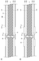
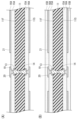
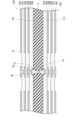
- FIG. 1 is a cross-sectional side view of a wiring board according to an embodiment of the present disclosure.
- Side cross section of the via land 1 is a side cross-sectional view showing a method for manufacturing a wiring board.
- 1 is a side cross-sectional view showing a method for manufacturing a wiring board.
- 1 is a side cross-sectional view showing a method for manufacturing a wiring board.
- 1 is a side cross-sectional view showing a method for manufacturing a wiring board.
- FIG. 13 is a cross-sectional side view of a wiring board according to a modified example.
- the wiring board 10 of this embodiment has a core board 11 and first and second build-up layers 12A, 12B laminated on both the front and back surfaces (first surface 11F and second surface 11S) of the core board 11.
- the core substrate 11 includes, for example, an insulating layer 11K and conductive layers 13 laminated on both sides of the insulating layer 11K.
- the insulating layer 11K has a structure in which, for example, multiple prepregs (B-stage resin sheets made by impregnating a core material made of fibers such as glass cloth with resin) are laminated.
- through-hole conductors 14 are formed in the insulating layer 11K.
- the first and second build-up layers 12A and 12B are formed by alternately stacking insulating layers 15 and conductive layers 16.
- the first insulating layer 15A, the first conductive layer 16A, the second insulating layer 15B, the second conductive layer 16B, the third insulating layer 15C, and the third conductive layer 16C are stacked in order from the core substrate 11 side.
- Each insulating layer 15 is, for example, an insulating film for a build-up substrate (a film having no core material, for example, made of a thermosetting resin containing an inorganic filler), and the conductive layer 16 is mainly electrolytic plating.
- first to third insulating layers 15A to 15C have via conductors 19 formed to connect the conductive layer 13 of the core substrate 11 to the first conductive layer 16A, between the first conductive layer 16A and the second conductive layer 16B, and between the second conductive layer 16B and the third conductive layer 16C, respectively.
- first and second buildup layers 12A and 12B have the same number of layers, but they may have different numbers of layers.
- a solder resist layer 17 having a number of openings 17A corresponding to the number of pads 18 included in the third conductive layer 16C is laminated on the first and second build-up layers 12A and 12B.
- each conductive layer 16 has a via land 20 (also called a "pad 20") connected through a via conductor 19 and a through-hole conductor 14, and a solid pattern 21 surrounding the via land 20.
- the via land 20, the via conductor 19, and the through-hole conductor 14 of each conductive layer 16 are aligned in the vertical direction, and the pad 18 on the first buildup layer 12A side is electrically connected to the pad 18 on the second buildup layer 12B side.
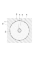
- the via land 20 has a circular shape in a plan view
- the solid pattern 21 has a circular opening 21A corresponding to the via land 20.
- the diameter of the opening 21A of the solid pattern 21 is 2 to 3 times the diameter of the via land 20, and the distance between the side of the via land 20 and the opening edge of the opening 21A of the solid pattern 21 is about 300 to 700 ⁇ m.
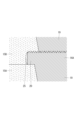
- the side surface of the via land 20 has a smaller roughness than the top surface of the via land 20.
- the insulating layer 15 is in close contact with the top surface of the via land 20, but is partially peeled off from the side surface of the via land 20, leaving a via land side gap 25 between the side surface of the via land 20 and the insulating layer 15.
- the inner surface of the opening 21A of the solid pattern 21 has a smaller roughness than the top surface of the solid pattern 21.
- the insulating layer 15 is in close contact with the top surface of the solid pattern 21, but is peeled off from the inner surface of the opening 21A of the solid pattern 21, and a solid pattern-side gap 26 (see FIG. 2) is provided between the inner surface of the opening 21A of the solid pattern 21 and the insulating layer 15.
- the lateral length of the via land side void 25 and the solid pattern side void 26 is about 0.01 to 0.1 ⁇ m. Note that although FIGS. 2 and 3 show the via land 20 and solid pattern 21 in the first conductive layer 16A on the first buildup layer 12A side, the via land side void 25 is also arranged on the side of the via land 20 in the second conductive layer 16B on the first buildup layer 12A side. The via land side void 25 may be arranged on the side of all the via lands 20, or may be arranged only on the side of some of the via lands 20. A gap may also be arranged between the via land 20 of the third conductive layer 16C and the solder resist layer 17.
- the via land side voids 25 and the solid pattern side voids 26 may be scattered as shown in FIG. 2, or may be disposed between the insulating layer 15 and the side of the via land 20 and the entire inner surface of the opening 21A of the solid pattern 21.
- the via land side voids 25 and the solid pattern side voids 26 may also be scattered in the vertical direction.
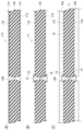
- a copper-clad laminate 11Z is prepared, in which copper foil 11C is laminated on both sides of an insulating layer 11K. As shown in FIG. 4(A), a laser is irradiated onto both sides of the copper-clad laminate 11Z to form through holes 14H.
- an insulating film for a build-up board is laminated as an insulating layer 15 on the conductive layers 13 on both the front and back of the core board 11 and then hot pressed. At this time, the non-patterned portions of the conductive layers 13 are filled with the insulating film. This forms insulating layers 15 (first insulating layers 15A) on both the front and back of the core board 11.
- a laser is irradiated to form a tapered via hole 19H penetrating the insulating layer 15, and the inside of the via hole 19H is cleaned (dry desmear process).
- an electroless plating process is performed to form an electroless plating film (not shown) on the insulating layer 15 and the inner surface of the via hole 19H.
- a plating resist 33 of a predetermined pattern is formed on the electroless plating film.
- an electrolytic plating process is performed, filling the via holes 19H with electrolytic plating to form via conductors 19, and forming electrolytic plating film 16M on the portions of the electroless plating film (not shown) on the first surface 11F and second surface 11S that are exposed from the plating resist 33.
- the plating resist 33 is peeled off.
- the electroless plating film below the plating resist 33 is removed, and the remaining electroless plating film and electrolytic plating film 16M form the conductive layer 16 (first conductive layer 16A).
- the first conductive layer 16A is provided with a via land 20 connected to a via conductor 19 that penetrates the first insulating layer 15A, and a solid pattern 21 that surrounds the via land 20.
- a protective film 35 is placed between the via land 20 and the solid pattern 21, and then the surface of the first conductive layer 16A is roughened.
- the side surface of the via land 20 and the inner surface of the opening 21A of the solid pattern 21 are not roughened, but the top surface of the via land 20 and the top surface of the solid pattern 21 are roughened, so that the roughness of the side surface of the via land 20 and the inner surface of the opening 21A of the solid pattern 21 is smaller than the roughness of the top surface of the via land 20 and the top surface of the solid pattern 21.
- an insulating film for a build-up board is laminated as the insulating layer 15 and then hot pressed. At that time, the non-patterned portions of the conductive layer 16, including the spaces between the via lands 20 and the solid pattern 21, are filled with the insulating film. This forms the insulating layer 15 (second insulating layer 15B) on the first conductive layer 16A.
- the portion of the insulating layer 15 between the via land 20 and the solid pattern 21 is partially peeled off from the side of the via land 20, which has a relatively small degree of roughness, and from the inner surface of the opening 21A of the solid pattern 21.
- a via land side gap 25 and a solid pattern side gap 26 are formed between the side of the via land 20 and the insulating layer 15, and between the inner surface of the opening 21A of the solid pattern 21 and the insulating layer 15, respectively.
- a solder resist layer 17 is laminated on the third conductive layer 16C.
- openings 17A are formed in predetermined locations of the solder resist layer 17, for example, by laser processing or photolithography processing.
- pads 18 are formed in the portions of the third conductive layer 16C that are exposed from the solder resist layer 17 by the openings 17A.
- a metal film is formed on the pad 18 by stacking a nickel layer, a palladium layer, and a gold layer in that order. This completes the wiring board 10 shown in Figure 1.
- the via lands 20 connected in the vertical direction through the via conductors 19 are surrounded by the solid pattern 21.
- stray capacitance occurs between the side surfaces of the via lands 20 and the solid pattern 21, it is thought that this will affect high-frequency signals.
- a via land side gap 25 is provided between the side of the via land 20 and the insulating layer 15, and the presence of air with a low dielectric constant reduces the stray capacitance that occurs. This also reduces the effect on high frequency signals.
- a solid pattern side gap 26 is provided between the inner surface of the opening 21A of the solid pattern 21 and the insulating layer 15, so the stray capacitance that occurs can be further reduced.
- a via land side gap 25 and a solid pattern side gap 26 can be selectively generated between the side surfaces when the insulating film serving as the insulating layer 15 is hot pressed, thereby suppressing the generation of unnecessary gaps (for example, the generation of a gap between the top surface of the via land 20 and the insulating layer 15).
- the via land side gap 25 is formed by reducing the roughness of the side surface of the via land 20.
- the via land side gap 25 may be formed by allowing the desmear liquid of the desmear process to enter the via hole 19H. In this case, it is considered that the via land side gap 25 is scattered on the upper surface and the side surface of the via land 20.
- multiple via lands 20 may be arranged within the opening 21A of the solid pattern 21, and multiple wiring may be arranged in the conductive layer 16.
- the distance between the via lands 20 or between the wiring is narrower than the distance between the side of the via land 20 and the inner surface of the opening 21A of the solid pattern 21, the volume of the resin of the insulating layer 15 arranged between the via lands 20 and between the wiring is small, and peeling due to thermal shrinkage is unlikely to occur.
- Only one of the via land side gap 25 and the solid pattern side gap 26 may be provided.
Landscapes
- Engineering & Computer Science (AREA)
- Microelectronics & Electronic Packaging (AREA)
- Manufacturing & Machinery (AREA)
- Production Of Multi-Layered Print Wiring Board (AREA)
Abstract
【課題】ランドの側面とベタパターンの側面との間に発生する浮遊容量を小さくすることが求められている。 【解決手段】本開示の配線基板は、第1導電層と、前記第1導電層を覆う絶縁層と、前記絶縁層上に形成される第2導電層と、前記絶縁層を貫通し、前記第1導電層と前記第2導電層を接続するビア導体と、を有する配線基板であって、前記第1導電層には、前記ビア導体と接続されるパッドと、前記パッドを内包する開口を有するベタパターンと、が設けられ、前記パッドの側面と前記絶縁層との間、または、前記ベタパターンの前記開口の内側面と前記絶縁層との間に、空隙が設けられている。
Description
本開示は、導電層同士がビア導体により接続されている配線基板に関する。
従来、この種の配線基板として、導電層同士を接続するビア導体のランドがベタパターンに囲まれているものが知られている(例えば、特許文献1参照)。
上述した従来の配線基板においては、ランドの側面とベタパターンの側面との間に発生する浮遊容量を小さくすることが求められている。
本開示の配線基板は、第1導電層と、前記第1導電層を覆う絶縁層と、前記絶縁層上に形成される第2導電層と、前記絶縁層を貫通し、前記第1導電層と前記第2導電層を接続するビア導体と、を有する配線基板であって、前記第1導電層には、前記ビア導体と接続されるパッドと、前記パッドを内包する開口を有するベタパターンと、が設けられ、前記パッドの側面と前記絶縁層との間、または、前記ベタパターンの前記開口の内側面と前記絶縁層との間に、空隙が設けられている。
以下、図1~図8を参照して本開示の一実施形態について説明する。図1に示すように、本実施形態の配線基板10は、コア基板11と、その表裏の両面(第1面11F、第2面11S)に積層される第1と第2のビルドアップ層12A,12Bとを有する。
コア基板11は、例えば、絶縁層11Kと、その表裏の両面に積層される導電層13とを備えている。絶縁層11Kは、例えば、複数のプリプレグ(ガラスクロス等の繊維からなる心材を樹脂含侵してなるBステージの樹脂シート)が積層された構造をなしている。また、絶縁層11Kには、スルーホール導体14が形成されている。
第1と第2のビルドアップ層12A,12Bは、絶縁層15と導電層16とが交互に積層されてなる。詳細には、それぞれ、コア基板11側から順番に、第1絶縁層15A、第1導電層16A、第2絶縁層15B、第2導電層16B、第3絶縁層15C、第3導電層16Cが積層されている。各絶縁層15は、例えば、ビルドアップ基板用の絶縁フィルム(心材を有さず、例えば、無機フィラーを含む熱硬化性樹脂からなるフィルム)であり、導電層16は、主として電解めっきである。また、第1~3の絶縁層15A~15Cには、コア基板11の導電層13と第1導電層16Aとの間、第1導電層16Aと第2導電層16Bとの間、第2導電層16Bと第3導電層16Cとの間をそれぞれ接続するビア導体19が形成されている。なお、本実施形態では、第1と第2のビルドアップ層12A,12Bは、同じ層数になっているが、互いに異なる層数であってもよい。
第1と第2のビルドアップ層12A,12Bの上には、第3導電層16Cに含まれる複数のパッド18に対応して複数の開口部17Aを有するソルダーレジスト層17が積層されている。
さて、本実施形態の配線基板10では、各導電層16が、ビア導体19及びスルーホール導体14を介して接続されるビアランド20(「パッド20」ともいう)と、ビアランド20を囲うベタパターン21と、を有している。各導電層16のビアランド20、ビア導体19及びスルーホール導体14は、上下方向で並んでいて、第1ビルドアップ層12A側のパッド18と第2ビルドアップ層12Bのパッド18とが電気的に接続されている。図2に示すように、ビアランド20は平面視円形状をなし、ベタパターン21には、ビアランド20に対応する円形の開口21Aが形成されている。ベタパターン21の開口21Aの径は、ビアランド20の径の2~3倍であり、ビアランド20の側面と、ベタパターン21の開口21Aの開口縁との間の距離は、300~700μm程である。
ここで、図3に示されるように、ビアランド20の側面は、ビアランド20の上面よりも粗度が小さくなっている。そして、絶縁層15は、ビアランド20の上面には密着している一方、ビアランド20の側面からは一部剥離していて、ビアランド20の側面と絶縁層15との間にビアランド側空隙25が設けられている。
同様に、ベタパターン21の開口21Aの内側面も、ベタパターン21の上面よりも粗度が小さくなっている。そして、絶縁層15は、ベタパターン21の上面には密着している一方、ベタパターン21の開口21Aの内側面からは剥離し、ベタパターン21の開口21Aの内側面と絶縁層15との間にベタパターン側空隙26(図2参照)が設けられている。
ビアランド側空隙25及びベタパターン側空隙26の横方向の長さは0.01~0.1μm程である。なお、図2及び図3には、第1のビルドアップ層12A側の第1導電層16Aにおけるビアランド20及びベタパターン21が例示されているが、ビアランド側空隙25は、第1のビルドアップ層12A側の第2導電層16Bにおけるビアランド20の側面にも配されている。また、ビアランド側空隙25は、全てのビアランド20の側面に配されていてもよいし、一部のビアランド20の側面にのみ配されていてもよい。また、第3導電層16Cのビアランド20とソルダーレジスト層17との間に空隙が配されていてもよい。
ビアランド側空隙25及びベタパターン側空隙26は、図2に示されるように、点在していてもよいし、絶縁層15とビアランド20の側面及びベタパターン21の開口21Aの内側面の全体との間に配されていてもよい。また、ビアランド側空隙25及びベタパターン側空隙26は、上下方向で点在していてもよい。
次に、配線基板10の製造方法について説明する。
(1)まず、絶縁層11Kの両面に銅箔11Cが積層されている銅張積層板11Zが用意され、図4(A)に示されるように、銅張積層板11Zの両面にレーザが照射されてスルーホール14Hが形成される。
(2)サブトラクティブ法により、絶縁層11Kの表裏の両面に銅箔11Cを含む導電層13が形成されると共に、スルーホール14Hの内面にスルーホール導体14が形成される(図4(B)参照)。これにより、コア基板11が形成される。
(3)次いで、コア基板11の表裏の両面の導電層13上に、絶縁層15としてビルドアップ基板用の絶縁フィルムが積層されて加熱プレスされる。その際、導電層13のパターンの非形成部分が絶縁フィルムにより埋められる。これにより、コア基板11の表裏の両面に絶縁層15(第1絶縁層15A)が形成される。
(4)図4(C)に示されるように、レーザが照射されて、絶縁層15を貫通するテーパー状のビアホール19Hが形成され、ビアホール19H内が洗浄(ドライデスミア処理)される。次いで、無電解めっき処理が行われ、絶縁層15上と、ビアホール19Hの内面とに無電解めっき膜(図示せず)が形成される。
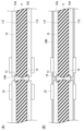
(5)図5(A)に示されるように、無電解めっき膜上に、所定パターンのめっきレジスト33が形成される。
(6)図5(B)に示されるように、電解めっき処理が行われ、ビアホール19H内に電解めっきが充填されてビア導体19が形成されると共に、第1面11F側及び第2面11S側の無電解めっき膜(図示せず)のうちめっきレジスト33から露出している部分に電解めっき膜16Mが形成される。
(7)図6(A)に示されるように、めっきレジスト33が剥離される。次いで、めっきレジスト33の下側の無電解めっき膜が除去され、残された無電解めっき膜及び電解めっき膜16Mにより、導電層16(第1導電層16A)が形成される。第1導電層16Aには、第1絶縁層15Aを貫通するビア導体19に接続されるビアランド20と、ビアランド20を囲うベタパターン21と、が設けられる。
(8)次いで、図6(B)に示されるように、ビアランド20とベタパターン21との間に保護膜35が配されたのち、第1導電層16Aの表面が粗化処理される。これにより、ビアランド20の側面及びベタパターン21の開口21Aの内側面は粗化されず、ビアランド20の上面及びベタパターン21の上面が粗化され、ビアランド20の側面及びベタパターン21の開口21Aの内側面の粗度がビアランド20の上面及びベタパターン21の上面の粗度よりも小さくなる。
(9)図7(A)に示されるように、保護膜35が除去される。
(10)図7(B)に示されるように、絶縁層15としてビルドアップ基板用の絶縁フィルムが積層されて加熱プレスされる。その際、ビアランド20とベタパターン21との間を含め、導電層16のパターンの非形成部分が絶縁フィルムにより埋められる。これにより、第1導電層16A上に絶縁層15(第2絶縁層15B)が形成される。
このとき、ビルドアップ基板用の絶縁フィルムの熱収縮により、絶縁層15のうちビアランド20とベタパターン21との間の部分が、粗度が比較的小さいビアランド20の側面及びベタパターン21の開口21Aの内側面から一部剥離する。これにより、ビアランド20の側面と絶縁層15との間及びベタパターン21の開口21Aの内側面と絶縁層15との間に、ビアランド側空隙25及びベタパターン側空隙26がそれぞれ形成される。
(11)上述した(4)~(10)と同様の工程が繰り返され、図8に示されるように、第2導電層16B、第3絶縁層15C、第3導電層16Cが形成される。
(12)第3導電層16C上に、ソルダーレジスト層17が積層される。次いで、ソルダーレジスト層17の所定箇所に、例えば、レーザ加工やフォトリソグラフィ処理等により、開口17Aが形成される。そして、第3導電層16Cのうち開口17Aによりソルダーレジスト層17から露出した部分にパッド18が形成される。
(13)パッド18上に、ニッケル層、パラジウム層、金層の順に積層されて金属膜が形成される。以上で図1に示される配線基板10が完成する。
次に配線基板10及びその製造方法の作用効果について説明する。本実施形態の配線基板10では、ビア導体19を介して上下方向で接続されたビアランド20がベタパターン21に囲まれている。ここで、ビアランド20とベタパターン21との側面同士の間に浮遊容量が発生すると高周波信号に影響が及ぶことが考えられる。
これに対して、本実施形態の配線基板10では、ビアランド20の側面と絶縁層15との間にビアランド側空隙25が設けられ、誘電率が低い空気が存在することで、発生する浮遊容量を小さくすることができる。これにより、高周波信号に対する影響も小さくすることができる。
しかも、ベタパターン21の開口21Aの内側面と絶縁層15との間にもベタパターン側空隙26が設けられているので、発生する浮遊容量をより小さくすることができる。
また、導電層16の粗化の段階でビアランド20の側面及びベタパターン21の開口21Aの内側面を保護しておくことで、絶縁層15としての絶縁フィルムを加熱プレスする際に側面同士の間にビアランド側空隙25及びベタパターン側空隙26を選択的に生じさせることができるので、不要な空隙の発生(例えば、ビアランド20の上面と絶縁層15との間の空隙の発生)を抑制することができる。
[他の実施形態]
(1)上記実施形態では、ビアランド側空隙25が、ビアランド20の側面の粗度を小さくすることにより形成されていたが、例えば、ビアホール19H内のデスミア処理のデスミア液を入り込ませることによって形成されてもよい。この場合、ビアランド20の上面上とビアランド20の側面上とにビアランド側空隙25が点在することになると考えられる。
(1)上記実施形態では、ビアランド側空隙25が、ビアランド20の側面の粗度を小さくすることにより形成されていたが、例えば、ビアホール19H内のデスミア処理のデスミア液を入り込ませることによって形成されてもよい。この場合、ビアランド20の上面上とビアランド20の側面上とにビアランド側空隙25が点在することになると考えられる。
(2)めっきレジスト33が配されている図5(B)の状態で、電解めっき膜16Mの上面の粗化が行われてもよい。この場合も、ビアランド20の側面と上面とで粗度に差を付けることができる。なお、この場合、保護膜35を形成する工程が不要となるので、製造工程が簡素化できるが、粗化の後に無電解めっき膜の除去処理(例えば、クイックエッチング)が行われることとなるため、粗化の際に、ビアランド20の上面の粗度が小さくなることを想定した粗度としておくことが必要になる。
(3)図9に示されるように、ベタパターン21の開口21A内に複数のビアランド20が配置されたり、導電層16において配線が複数並ぶ箇所があってもよい。この場合、ビアランド20間や配線間の距離が、ビアランド20の側面とベタパターン21の開口21Aの内側面との間の距離よりも狭い間隔で並んでいれば、ビアランド20間及び配線間に配される絶縁層15の樹脂の体積が小さく、熱収縮による剥離が起きにくいと考えられる。
(4)配線基板10は、コアレス構造であってもよい。
(5)ビアランド側空隙25とベタパターン側空隙26とのうち一方のみが設けられていてもよい。
なお、本明細書及び図面には、特許請求の範囲に含まれる技術の具体例が開示されているが、特許請求の範囲に記載の技術は、これら具体例に限定されるものではなく、具体例を様々に変形、変更したものも含み、また、具体例から一部を単独で取り出したものも含む。
10 配線基板
15 絶縁層
15A 第1絶縁層
15B 第2絶縁層
16 導電層
16A 第1導電層
16B 第2導電層
19 ビア導体
20 ビアランド
21 ベタパターン
21A 開口
25 ビアランド側空隙
26 ベタパターン側空隙
35 保護膜
15 絶縁層
15A 第1絶縁層
15B 第2絶縁層
16 導電層
16A 第1導電層
16B 第2導電層
19 ビア導体
20 ビアランド
21 ベタパターン
21A 開口
25 ビアランド側空隙
26 ベタパターン側空隙
35 保護膜
Claims (7)
- 第1導電層と、
前記第1導電層を覆う絶縁層と、
前記絶縁層上に形成される第2導電層と、
前記絶縁層を貫通し、前記第1導電層と前記第2導電層を接続するビア導体と、を有する配線基板であって、
前記第1導電層には、前記ビア導体と接続されるパッドと、前記パッドを内包する開口を有するベタパターンと、が設けられ、
前記パッドの側面と前記絶縁層との間、または、前記ベタパターンの前記開口の内側面と前記絶縁層との間に、空隙が設けられている。 - 請求項1に記載の配線基板であって、
前記パッドの側面と前記絶縁層との間、および、前記ベタパターンの前記開口の内側面と前記絶縁層との間に、空隙が設けられている。 - 請求項1に記載の配線基板であって、
前記パッドの側面の粗度が、前記パッドの上面の粗度よりも小さい。 - 請求項1に記載の配線基板であって、
前記空隙は、複数の箇所に点在している。 - 請求項1に記載の配線基板であって、
前記空隙の最大幅は、0.01~0.1μmである。 - 請求項1に記載の配線基板であって、
前記パッドの側面と前記ベタパターンの前記開口の内側面との間の距離は300~700μmである。 - 請求項1に記載の配線基板であって、
前記ベタパターンの前記開口の径が前記パッドの径の2~3倍である。
Priority Applications (1)
| Application Number | Priority Date | Filing Date | Title |
|---|---|---|---|
| CN202480019045.5A CN120826987A (zh) | 2023-06-05 | 2024-06-03 | 布线基板 |
Applications Claiming Priority (2)
| Application Number | Priority Date | Filing Date | Title |
|---|---|---|---|
| JP2023-092463 | 2023-06-05 | ||
| JP2023092463A JP2024174570A (ja) | 2023-06-05 | 2023-06-05 | 配線基板 |
Publications (1)
| Publication Number | Publication Date |
|---|---|
| WO2024253055A1 true WO2024253055A1 (ja) | 2024-12-12 |
Family
ID=93795961
Family Applications (1)
| Application Number | Title | Priority Date | Filing Date |
|---|---|---|---|
| PCT/JP2024/020166 Ceased WO2024253055A1 (ja) | 2023-06-05 | 2024-06-03 | 配線基板 |
Country Status (3)
| Country | Link |
|---|---|
| JP (1) | JP2024174570A (ja) |
| CN (1) | CN120826987A (ja) |
| WO (1) | WO2024253055A1 (ja) |
Citations (4)
| Publication number | Priority date | Publication date | Assignee | Title |
|---|---|---|---|---|
| JP2003298195A (ja) * | 2002-04-03 | 2003-10-17 | Ngk Spark Plug Co Ltd | 配線基板 |
| JP2017011093A (ja) * | 2015-06-22 | 2017-01-12 | イビデン株式会社 | プリント配線板 |
| JP2021168349A (ja) * | 2020-04-10 | 2021-10-21 | イビデン株式会社 | 部品内蔵配線基板 |
| JP2022084352A (ja) * | 2020-11-26 | 2022-06-07 | 三菱電機株式会社 | プリント配線板 |
-
2023
- 2023-06-05 JP JP2023092463A patent/JP2024174570A/ja active Pending
-
2024
- 2024-06-03 WO PCT/JP2024/020166 patent/WO2024253055A1/ja not_active Ceased
- 2024-06-03 CN CN202480019045.5A patent/CN120826987A/zh active Pending
Patent Citations (4)
| Publication number | Priority date | Publication date | Assignee | Title |
|---|---|---|---|---|
| JP2003298195A (ja) * | 2002-04-03 | 2003-10-17 | Ngk Spark Plug Co Ltd | 配線基板 |
| JP2017011093A (ja) * | 2015-06-22 | 2017-01-12 | イビデン株式会社 | プリント配線板 |
| JP2021168349A (ja) * | 2020-04-10 | 2021-10-21 | イビデン株式会社 | 部品内蔵配線基板 |
| JP2022084352A (ja) * | 2020-11-26 | 2022-06-07 | 三菱電機株式会社 | プリント配線板 |
Also Published As
| Publication number | Publication date |
|---|---|
| JP2024174570A (ja) | 2024-12-17 |
| CN120826987A (zh) | 2025-10-21 |
Similar Documents
| Publication | Publication Date | Title |
|---|---|---|
| JP5272090B2 (ja) | 配線板とその製造方法 | |
| KR101375998B1 (ko) | 다층 배선기판의 제조방법 및 다층 배선기판 | |
| KR101290471B1 (ko) | 다층 배선 기판 및 그 제조방법 | |
| KR101215246B1 (ko) | 다층 배선기판의 제조방법 및 다층 배선기판 | |
| KR101281410B1 (ko) | 다층 배선기판 | |
| JP5566771B2 (ja) | 多層配線基板 | |
| JP7159059B2 (ja) | 積層基板及び積層基板製造方法 | |
| TWI478642B (zh) | 具有內埋元件的電路板及其製作方法 | |
| JP2018006386A (ja) | 配線板の製造方法 | |
| JP2012094662A (ja) | 多層配線基板の製造方法 | |
| CN104472024A (zh) | 用于具有嵌入式电缆的印刷电路板的设备和方法 | |
| JP2018018935A (ja) | プリント配線板及びその製造方法 | |
| KR20130098921A (ko) | 다층 배선기판 및 그 제조방법 | |
| KR100832650B1 (ko) | 다층 인쇄회로기판 및 그 제조 방법 | |
| JP5147872B2 (ja) | 回路構造の製造方法 | |
| KR101987378B1 (ko) | 인쇄회로기판의 제조 방법 | |
| JP2011181542A (ja) | 多層配線基板及びその製造方法 | |
| JP5865769B2 (ja) | 多層配線基板の製造方法 | |
| JP2022119655A (ja) | 配線基板 | |
| WO2024253055A1 (ja) | 配線基板 | |
| JP2013131731A (ja) | 配線基板およびその製造方法 | |
| JP2000323841A (ja) | 多層回路基板とその製造方法 | |
| JP2011222962A (ja) | プリント基板およびその製造方法 | |
| KR101108816B1 (ko) | 다층 인쇄회로기판 및 이의 제조방법 | |
| JP2020141036A (ja) | 印刷配線板及び印刷配線板の製造方法 |
Legal Events
| Date | Code | Title | Description |
|---|---|---|---|
| 121 | Ep: the epo has been informed by wipo that ep was designated in this application |
Ref document number: 24819285 Country of ref document: EP Kind code of ref document: A1 |
|
| WWE | Wipo information: entry into national phase |
Ref document number: 202480019045.5 Country of ref document: CN |
|
| WWP | Wipo information: published in national office |
Ref document number: 202480019045.5 Country of ref document: CN |
|
| NENP | Non-entry into the national phase |
Ref country code: DE |