WO2024252863A1 - 積層セラミックコンデンサ - Google Patents
積層セラミックコンデンサ Download PDFInfo
- Publication number
- WO2024252863A1 WO2024252863A1 PCT/JP2024/017777 JP2024017777W WO2024252863A1 WO 2024252863 A1 WO2024252863 A1 WO 2024252863A1 JP 2024017777 W JP2024017777 W JP 2024017777W WO 2024252863 A1 WO2024252863 A1 WO 2024252863A1
- Authority
- WO
- WIPO (PCT)
- Prior art keywords
- via conductors
- internal electrode
- main surface
- multilayer ceramic
- ceramic capacitor
- Prior art date
- Legal status (The legal status is an assumption and is not a legal conclusion. Google has not performed a legal analysis and makes no representation as to the accuracy of the status listed.)
- Ceased
Links
Images


Classifications
-
- H—ELECTRICITY
- H01—ELECTRIC ELEMENTS
- H01G—CAPACITORS; CAPACITORS, RECTIFIERS, DETECTORS, SWITCHING DEVICES, LIGHT-SENSITIVE OR TEMPERATURE-SENSITIVE DEVICES OF THE ELECTROLYTIC TYPE
- H01G4/00—Fixed capacitors; Processes of their manufacture
- H01G4/30—Stacked capacitors
-
- H—ELECTRICITY
- H01—ELECTRIC ELEMENTS
- H01G—CAPACITORS; CAPACITORS, RECTIFIERS, DETECTORS, SWITCHING DEVICES, LIGHT-SENSITIVE OR TEMPERATURE-SENSITIVE DEVICES OF THE ELECTROLYTIC TYPE
- H01G4/00—Fixed capacitors; Processes of their manufacture
- H01G4/002—Details
- H01G4/005—Electrodes
- H01G4/012—Form of non-self-supporting electrodes
-
- H—ELECTRICITY
- H01—ELECTRIC ELEMENTS
- H01G—CAPACITORS; CAPACITORS, RECTIFIERS, DETECTORS, SWITCHING DEVICES, LIGHT-SENSITIVE OR TEMPERATURE-SENSITIVE DEVICES OF THE ELECTROLYTIC TYPE
- H01G4/00—Fixed capacitors; Processes of their manufacture
- H01G4/002—Details
- H01G4/228—Terminals
- H01G4/232—Terminals electrically connecting two or more layers of a stacked or rolled capacitor
Definitions
- the present invention relates to a multilayer ceramic capacitor.
- Patent Document 1 JP 2009-295687 A (Patent Document 1) is a prior art document that discloses the configuration of an electronic component for incorporation into a wiring board.
- the electronic component for incorporation into a wiring board described in Patent Document 1 comprises a ceramic sintered body and an external electrode.
- the ceramic sintered body has a main surface and a back surface.
- the external electrode is disposed on at least one of the main surface and back surface of the ceramic sintered body, and is formed by forming a copper plating layer on the surface of the metallized metal layer.
- the ceramic sintered body has a plurality of internal electrodes stacked with ceramic dielectric layers interposed therebetween, and has a plurality of via conductors in a capacitor connected to the plurality of internal electrodes.
- the external electrode is connected to at least one end of the main surface side and the back surface side of the plurality of via conductors in a capacitor.
- the plurality of via conductors in a capacitor are arranged in an array as a whole.
- the present invention has been made in consideration of the above problems, and aims to provide a multilayer ceramic capacitor with high capacitance density, in which multiple capacitor functional parts that can be connected to power sources with different potentials are densely arranged in parallel.
- the multilayer ceramic capacitor according to the present invention comprises a capacitor body, a plurality of first via conductors, a plurality of second via conductors, a plurality of first external electrodes, and at least one second external electrode.
- the capacitor body includes a plurality of first internal electrode layers and a plurality of second internal electrode layers that are alternately stacked in a stacking direction with a dielectric layer sandwiched between them, and has a first main surface and a second main surface located on the opposite side of the stacking direction from the first main surface.
- the plurality of first via conductors are provided inside the capacitor body and are electrically connected to the plurality of first internal electrode layers.
- the plurality of second via conductors are provided inside the capacitor body and are electrically connected to the plurality of second internal electrode layers.
- the plurality of first external electrodes and at least one second external electrode are provided at intervals from each other on the first main surface.
- Each of the plurality of first internal electrode layers is composed of a plurality of first internal electrode portions that are spaced apart from each other within the same layer.
- Each of the plurality of second internal electrode layers is integrally formed within the same layer.
- Each of the first internal electrode portions is electrically connected to a corresponding one of the first via conductors.
- Each of the first external electrodes is electrically connected to a corresponding one of the first internal electrode portions.
- At least one second external electrode is electrically connected to a corresponding one of the second via conductors.
- the present invention makes it possible to realize a multilayer ceramic capacitor with high capacitance density, in which multiple capacitor functional parts that can be connected to power sources with different potentials are densely arranged in parallel.
- FIG. 1 is a perspective view of a multilayer ceramic capacitor according to a first embodiment of the present invention, as viewed from a first main surface side.
- FIG. 2 is a plan view of the multilayer ceramic capacitor of FIG. 1 as viewed from a direction II.
- 3 is a cross-sectional view of the multilayer ceramic capacitor of FIG. 2 as viewed from the direction of the arrows III-III.
- FIG. 2 is a plan view of the capacitor body.
- 4 is a cross-sectional view of the multilayer ceramic capacitor of FIG. 3 as viewed from the direction of the arrows VV.
- 6 is a cross-sectional view of the multilayer ceramic capacitor of FIG. 3 as viewed from the direction of the arrows along line VI-VI.
- FIG. 1 is a perspective view of a multilayer ceramic capacitor according to a first embodiment of the present invention, as viewed from a first main surface side.
- FIG. 2 is a plan view of the multilayer ceramic capacitor of FIG. 1 as viewed from
- FIG. 2 is a plan view of a multilayer ceramic capacitor according to a first modified example of the first embodiment of the present invention.
- 8 is a side view of the multilayer ceramic capacitor of FIG. 7 as viewed in the direction of arrow VIII.
- 8 is a side view of the multilayer ceramic capacitor of FIG. 7 as viewed in the direction of arrow IX.
- FIG. 11 is a perspective view of a multilayer ceramic capacitor according to a second modified example of the first preferred embodiment of the present invention, as viewed from a second main surface side.
- 11 is a cross-sectional view of the multilayer ceramic capacitor of FIG. 10 as viewed from the direction of the arrows along line XI-XI.
- FIG. 11 is a perspective view of a multilayer ceramic capacitor according to a third modified example of the first preferred embodiment of the present invention, as viewed from a second main surface side.
- 13 is a cross-sectional view of the multilayer ceramic capacitor of FIG. 12 as viewed from the direction of the arrows along line XIII-XIII.
- 14 is a cross-sectional view of the multilayer ceramic capacitor of FIG. 12 as viewed from the direction of the arrows along line XIV-XIV.
- FIG. 11 is a perspective view of a multilayer ceramic capacitor according to a second embodiment of the present invention, as viewed from a first main surface side.
- FIG. 5 is an exploded perspective view showing a configuration of a multilayer ceramic capacitor according to a second embodiment of the present invention.
- FIG. 17 is a perspective view of the multilayer ceramic capacitor of FIG. 16 as viewed from a direction XVII.
- 18 is a cross-sectional view of the multilayer ceramic capacitor of FIG. 17 as viewed from the direction of the arrows along line XVIII-XVIII.
- 18 is a cross-sectional view of the multilayer ceramic capacitor of FIG. 17 as viewed from the direction of the arrows along line XIX-XIX.
- 18 is a cross-sectional view of the multilayer ceramic capacitor of FIG. 17, taken along the line XX-XX.
- Fig. 1 is a perspective view of a multilayer ceramic capacitor according to a first embodiment of the present invention, as viewed from the first main surface side.
- Fig. 2 is a plan view of the multilayer ceramic capacitor of Fig. 1, as viewed from direction II.
- Fig. 3 is a cross-sectional view of the multilayer ceramic capacitor of Fig. 2, as viewed from the direction of the arrows III-III.
- Fig. 4 is a plan view of a capacitor body.
- Fig. 5 is a cross-sectional view of the multilayer ceramic capacitor of Fig. 3, as viewed from the direction of the arrows V-V.
- Fig. 6 is a cross-sectional view of the multilayer ceramic capacitor of Fig. 3, as viewed from the direction of the arrows VI-VI.
- the multilayer ceramic capacitor 1 according to embodiment 1 of the present invention comprises a capacitor body 100, a plurality of first via conductors 140, a plurality of second via conductors 150, a plurality of first external electrodes 20, and at least one second external electrode 30.
- the capacitor body 100 includes a plurality of first internal electrode layers 120 and a plurality of second internal electrode layers 130 that are alternately stacked in the stacking direction with dielectric layers 110 sandwiched between them, and has a first main surface 101 and a second main surface 102 that is located on the opposite side of the first main surface 101 in the stacking direction.
- the dielectric layer 110 may be made of any material, and may be made of, for example, a ceramic material mainly composed of BaTiO3 , CaTiO3 , SrTiO3 , SrZrO3 , or CaZrO3 .
- These main components may contain a minor component selected from the group consisting of Mn compounds, Fe compounds, Cr compounds, Co compounds, and Ni compounds, the minor component being contained in a smaller amount than the main component.
- the capacitor body 100 may have any shape.
- the capacitor body 100 has a rectangular parallelepiped shape as a whole.
- An overall rectangular parallelepiped shape is one that is not a perfect rectangular parallelepiped shape, for example, one in which the corners and edges of the rectangular parallelepiped are rounded, but has six surfaces and can be considered as a rectangular parallelepiped as a whole.
- the capacitor body 100 has a first main surface 101, a second main surface 102, a first side surface 103, a second side surface 104, a third side surface 105, and a fourth side surface 106.
- the first side surface 103 to the fourth side surface 106 of the capacitor body 100 constitute four side surfaces of the surface of the capacitor body 100 other than the first main surface 101 and the second main surface 102. That is, the capacitor body 100 further has the first side surface 103 to the fourth side surface 106, which are four side surfaces connecting the first main surface 101 and the second main surface 102.
- the first side surface 103 faces the second side surface 104
- the third side surface 105 faces the fourth side surface 106.
- the first side surface 103 to the fourth side surface 106 of the capacitor body 100 are perpendicular to each of the first main surface 101 and the second main surface 102, but they do not have to be perpendicular to each other.
- the dimensions of the capacitor body 100 are arbitrary, but for example, when viewed from the first main surface 101 side, the vertical dimension of the rectangle can be 0.3 mm to 3.0 mm, the horizontal dimension can be 0.3 mm to 3.0 mm, and the dimensions in the stacking direction of the dielectric layer 110, the first internal electrode layer 120, and the second internal electrode layer 130 can be 50 ⁇ m to 200 ⁇ m.
- the dimensions of the capacitor body 100 in the stacking direction refer to the thickness of the capacitor body 100.
- each of the first internal electrode layers 120 is composed of a plurality of first internal electrode parts spaced apart from each other in the same layer.
- each of the first internal electrode layers 120 is composed of a first internal electrode part 121 and a first internal electrode part 122 spaced apart from each other in the same layer.
- the first internal electrode part 121 and the first internal electrode part 122 have a line-symmetric shape.
- the shapes of the first internal electrode part 121 and the first internal electrode part 122 are not limited to line-symmetric shapes and may be asymmetric shapes.
- the number of first internal electrode parts arranged in the same layer is not limited to two and may be three or more.
- Each of the first internal electrode layers 120 has a plurality of first through holes 120h formed therein to insert a plurality of second via conductors 150 described later.
- each of the multiple second internal electrode layers 130 is integrally formed within the same layer.
- the second internal electrode layer 130 has a rectangular outer shape that is approximately the same as the first internal electrode layer 120.
- Each of the multiple second internal electrode layers 130 has multiple second through holes 130h formed therein to allow multiple first via conductors 140, which will be described later, to pass through.
- the material of the first internal electrode layer 120 and the second internal electrode layer 130 is arbitrary, and may contain, for example, a metal such as Ni, Cu, Ag, Pd, Pt, Fe, Ti, Cr, Sn, or Au, or an alloy containing these metals, as a main component.
- the first internal electrode layer 120 and the second internal electrode layer 130 may contain, as a common material, the same ceramic material as the dielectric ceramic contained in the dielectric layer 110. In that case, the proportion of the common material contained in the first internal electrode layer 120 and the second internal electrode layer 130 is, for example, 20 vol % or less.
- each of the first internal electrode layer 120 and the second internal electrode layer 130 is arbitrary, but can be, for example, about 0.3 ⁇ m or more and 1.0 ⁇ m or less.
- the number of layers of the first internal electrode layer 120 and the second internal electrode layer 130 is arbitrary, but can be, for example, about 10 layers or more and 150 layers or less in total.
- the first internal electrode layer 120 and the second internal electrode layer 130 face each other via the dielectric layer 110, forming a capacitance.
- the first internal electrode layer 120 and the second internal electrode layer 130 face each other via the dielectric layer 110, forming a capacitance.
- the multiple first via conductors 140 are provided inside the capacitor body 100 and are electrically connected to the multiple first internal electrode layers 120.
- the multiple first via conductors 140 pass through second through holes 130h formed in each of the multiple second internal electrode layers 130, and are insulated from the multiple second internal electrode layers 130.
- the multiple first via conductors 140 are arranged in multiple rows.
- each of the multiple first internal electrode portions is electrically connected to a corresponding multiple first via conductors 140 among the multiple first via conductors 140.
- the first internal electrode portion 121 is electrically connected to three corresponding first via conductors 140 arranged in a row.
- the first internal electrode portion 122 is electrically connected to the other three corresponding first via conductors 140 arranged in a row.
- Each of the multiple first via conductors 140 is provided inside the capacitor body 100 in a manner that extends in the stacking direction from the first main surface 101 to the second main surface 102 of the capacitor body 100. In other words, each of the multiple first via conductors 140 is exposed to the first main surface 101 of the capacitor body 100, but is not exposed to the second main surface 102. This makes it possible to prevent a short circuit from occurring between the electronic component arranged on the second main surface 102 side and the multilayer ceramic capacitor 1.
- the multiple second via conductors 150 are provided inside the capacitor body 100 and are electrically connected to the multiple second internal electrode layers 130.
- the multiple second via conductors 150 pass through first through holes 120h formed in each of the multiple first internal electrode layers 120, and are insulated from the multiple first internal electrode layers 120.
- the multiple second via conductors 150 are arranged in rows between the rows of the multiple first via conductors 140.
- the first via conductors 140 and the second via conductors 150 are arranged in a matrix.
- the second internal electrode layer 130 is electrically connected to three second via conductors 150 arranged in one row.
- Each of the multiple second via conductors 150 is provided inside the capacitor body 100 in a manner that extends in the stacking direction from the first main surface 101 to the second main surface 102 of the capacitor body 100. That is, each of the multiple second via conductors 150 is exposed to the first main surface 101 of the capacitor body 100, but is not exposed to the second main surface 102.
- the magnetic fields induced by the currents flowing through the first via conductors 140 and the second via conductors 150 cancel each other out, thereby lowering the equivalent series inductance (ESL) of the multilayer ceramic capacitor 1.
- the first via conductor 140 and the second via conductor 150 may have any shape, for example, a cylindrical shape.
- the diameter of the first via conductor 140 and the second via conductor 150 is, for example, about 30 ⁇ m or more and 150 ⁇ m or less.
- the distance between adjacent first via conductors 140 and second via conductors 150, more specifically, the distance between the center of the first via conductor 140 and the center of the second via conductor 150 is, for example, about 50 ⁇ m or more and 500 ⁇ m or less.
- the material of the first via conductor 140 and the second via conductor 150 is arbitrary, and for example, metals such as Ni, Cu, Ag, Pd, Pt, Fe, Ti, Cr, Sn, or Au, or alloys containing these metals, can be used.
- Each of the multiple first external electrodes 20 extends in a rectangular shape.
- the shape of each of the multiple first external electrodes 20 is not limited to a rectangular shape, and may be a trapezoid, L-shape, U-shape, X-shape, T-shape, or the like.
- Each of the multiple first external electrodes 20 is electrically connected to multiple first via conductors 140 that are electrically connected to a corresponding first internal electrode portion among the multiple first internal electrode portions.
- the first external electrode 21 is electrically connected to three first via conductors 140 that are electrically connected to the corresponding first internal electrode portion 121.
- the first external electrode 22 is electrically connected to three first via conductors 140 that are electrically connected to the corresponding first internal electrode portion 122.
- the connection relationship between the first external electrode 20 and the first via conductors 140 is not limited to the above, and it is sufficient that multiple first via conductors 140 that are electrically connected to the corresponding first internal electrode portion are connected to each first external electrode 20.
- At least one second external electrode 30 extends in a rectangular shape.
- the shape of the second external electrode 30 is not limited to a rectangular shape, and may be a trapezoid, an L-shape, a U-shape, an X-shape, a T-shape, or the like.
- At least one second external electrode 30 is electrically connected to a corresponding number of second via conductors 150 among the plurality of second via conductors 150.
- one second external electrode 30 is electrically connected to all three second via conductors 150.
- the connection relationship between the second external electrode 30 and the second via conductors 150 is not limited to the above, and it is sufficient that a corresponding number of second via conductors 150 are connected to each second external electrode 30.
- the first external electrode 20 and the second external electrode 30 may be made of any material.
- the first external electrode 20 and the second external electrode 30 are plated electrodes formed by a plating process using a rotary plating method. Examples of materials that may form the plated electrodes include Cu, Ni, and Sn.
- the plated electrodes may be formed of a single layer or multiple layers.
- each of the first internal electrode layers 120 is composed of a first internal electrode portion 121 and a first internal electrode portion 122 that are spaced apart from each other in the same layer.
- Each of the second internal electrode layers 130 is integrally composed in the same layer.
- Each of the first internal electrode portion 121 and the first internal electrode portion 122 is electrically connected to a corresponding one of the first via conductors 140.
- Each of the first external electrode 21 and the first external electrode 22 is electrically connected to a corresponding one of the first internal electrode portions 121 and the first internal electrode portion 122.
- At least one second external electrode 30 is electrically connected to a corresponding one of the second via conductors 150.
- a capacitor functional section consisting of the first internal electrode section 121 and the second internal electrode layer 130 facing each other across the dielectric layer 110, and another capacitor functional section consisting of the first internal electrode section 122 and the second internal electrode layer 130 facing each other across the dielectric layer 110, can be arranged side by side at high density, thereby realizing a multilayer ceramic capacitor 1 with high capacitance density.
- each first external electrode 20 is electrically connected to a plurality of first via conductors 140 and each second external electrode 30 is electrically connected to a plurality of second via conductors 150
- each of the first external electrodes 20 and second external electrodes 30 can be easily connected to a connection terminal such as an IC and can be connected over the shortest distance compared to a case where each of the first via conductors 140 and second via conductors 150 is connected to a connection terminal such as an IC on a one-to-one basis.
- the present invention is particularly effective when the pitch between connection terminals such as ICs is short.
- the first via conductors 140 are arranged in a plurality of rows.
- the second via conductors 150 are arranged in rows between the rows of the first via conductors 140, thereby making it possible to reduce the ESL of the multilayer ceramic capacitor 1.
- the second external electrode 30 is disposed between the first external electrodes 20, so that the first external electrode 20 and the second external electrode 30 can be easily visually distinguished from each other regardless of the orientation of the multilayer ceramic capacitor 1.
- the orientation of the multilayer ceramic capacitor 1 means, for example, the vertical orientation shown in FIG. 2 and the horizontal orientation shown in FIG. 2 rotated 90°.
- FIG. 7 is a plan view of a multilayer ceramic capacitor according to a first modified example of embodiment 1 of the present invention.
- FIG. 8 is a side view of the multilayer ceramic capacitor of FIG. 7 as viewed from the direction of arrow VIII.
- FIG. 9 is a side view of the multilayer ceramic capacitor of FIG. 7 as viewed from the direction of arrow IX.
- the multilayer ceramic capacitor 1A includes a plurality of first external electrodes 20A and at least one second external electrode 30A.
- the first external electrode 20A is composed of a first external electrode 21A and a first external electrode 22A.
- Each of the plurality of first external electrodes 20A extends from the first main surface 101 onto at least one of the four side surfaces.
- At least one second external electrode 30A extends from the first main surface 101 onto at least one of the four side surfaces.
- the first external electrode 21A is formed from the first main surface 101 to the first side surface 103, the third side surface 105, and the fourth side surface 106.
- the first external electrode 21A covers the ridge portion between the first main surface 101 and the first side surface 103.
- the first external electrode 22A is formed from the first main surface 101 to the second side surface 104, the third side surface 105, and the fourth side surface 106.
- the first external electrode 22A covers the ridge portion between the first main surface 101 and the second side surface 104.
- the second external electrode 30A is formed from the first main surface 101 to the third side surface 105 and the fourth side surface 106.
- the corners or ridges of the capacitor body 100 can be covered with the first external electrode 20A and the second external electrode 30A, which can prevent cracks or chips from occurring at the corners or ridges of the capacitor body 100.
- the corners or ridges of the capacitor body 100 can be covered with the first external electrode 20A and the second external electrode 30A, which can prevent cracks or chips from occurring at the corners or ridges of the capacitor body 100.
- by contacting a probe with each of the first external electrode 20A and the second external electrode 30A formed on the side surface of the capacitor body 100 it is possible to measure the electrical characteristics of the multilayer ceramic capacitor 1A.
- the first external electrode 20A and the second external electrode 30A may be formed, for example, by a sputtering method, a vapor deposition method, or a method of baking metal powder or metal powder paste.
- FIG. 10 is a perspective view of a multilayer ceramic capacitor according to a second modified example of the first embodiment of the present invention, viewed from the second main surface side.
- FIG. 11 is a cross-sectional view of the multilayer ceramic capacitor of FIG. 10, viewed from the direction of the arrows along line XI-XI.
- the multilayer ceramic capacitor 1B according to the second modified example of the first embodiment of the present invention includes a plurality of first via conductors 140B and a plurality of second via conductors 150B provided inside the capacitor body 100B.
- the first via conductors 140B and the second via conductors 150B are arranged in a matrix.
- Each of the multiple first via conductors 140B is exposed to the first principal surface 101 and also to the second principal surface 102 of the capacitor body 100B. Specifically, each of the multiple first via conductors 140B is arranged to penetrate the capacitor body 100B in the stacking direction. One end of each of the multiple first via conductors 140B in the stacking direction is connected to the first external electrode 20, and the other end protrudes from the second principal surface 102. Note that the other end of each of the multiple first via conductors 140B does not necessarily have to protrude from the second principal surface 102, and may be located flush with the second principal surface 102.
- Each of the multiple second via conductors 150B is exposed to the first principal surface 101 and also to the second principal surface 102 of the capacitor body 100B. Specifically, each of the multiple second via conductors 150B is arranged to penetrate the capacitor body 100B in the stacking direction. One end of each of the multiple second via conductors 150B in the stacking direction is connected to the second external electrode 30, and the other end protrudes from the second principal surface 102. Note that the other end of each of the multiple second via conductors 150B does not necessarily have to protrude from the second principal surface 102, and may be located flush with the second principal surface 102.
- each of the multiple first via conductors 140B and the multiple second via conductors 150B is exposed on the second principal surface 102 side. This makes it possible to electrically connect the electronic component connected to the first principal surface 101 side and the electronic component connected to the second principal surface 102 side via the multilayer ceramic capacitor 1B.
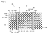
- FIG. 12 is a perspective view of a multilayer ceramic capacitor according to a third modified example of the first embodiment of the present invention, viewed from the second main surface side.
- FIG. 13 is a cross-sectional view of the multilayer ceramic capacitor of FIG. 12, viewed from the direction of the arrows along line XIII-XIII.
- FIG. 14 is a cross-sectional view of the multilayer ceramic capacitor of FIG. 12, viewed from the direction of the arrows along line XIV-XIV.
- the multilayer ceramic capacitor 1C according to the third modified example of the first embodiment of the present invention includes a plurality of first via conductors 140C and a plurality of second via conductors 150C provided inside the capacitor body 100C.
- the first via conductors 140C and the second via conductors 150C are arranged at different positions in the column direction.
- each of the plurality of first via conductors 140C and the plurality of second via conductors 150C is exposed on the second principal surface 102 side. This makes it possible to electrically connect an electronic component connected to the first principal surface 101 side and an electronic component connected to the second principal surface 102 side via the multilayer ceramic capacitor 1C.
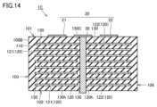
- the multilayer ceramic capacitor according to the second embodiment of the present invention differs from the multilayer ceramic capacitor according to the first embodiment of the present invention mainly in the arrangement of the first external electrodes, the second external electrodes, the first via conductors, and the second via conductors, and in further including an insulating layer, and therefore the same components as those in the multilayer ceramic capacitor according to the first embodiment of the present invention will be given the same reference numerals and description thereof will not be repeated.
- FIG. 15 is a perspective view of a multilayer ceramic capacitor according to embodiment 2 of the present invention, as viewed from the first main surface side.
- FIG. 16 is an exploded perspective view showing the configuration of a multilayer ceramic capacitor according to embodiment 2 of the present invention.
- FIG. 17 is a perspective view of the multilayer ceramic capacitor of FIG. 16, as viewed from the XVII direction.
- FIG. 18 is a cross-sectional view of the multilayer ceramic capacitor of FIG. 17, as viewed from the direction of the XVIII-XVIII arrows.
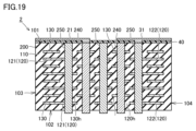
- FIG. 19 is a cross-sectional view of the multilayer ceramic capacitor of FIG. 17, as viewed from the direction of the XIX-XIX arrows.
- FIG. 20 is a cross-sectional view of the multilayer ceramic capacitor of FIG. 17, as viewed from the direction of the XX-XX arrows.
- the multilayer ceramic capacitor 2 according to the second embodiment of the present invention comprises a capacitor body 200, a plurality of first via conductors 240, a plurality of second via conductors 250, a plurality of first external electrodes 20 and a plurality of second external electrodes 30, and an insulating layer 40.
- the multilayer ceramic capacitor 2 includes a plurality of first via conductors 240 and a plurality of second via conductors 250 provided inside the capacitor body 200.
- the plurality of first via conductors 240 and the plurality of second via conductors 250 are arranged alternately in both the row direction and the column direction.
- Each of the multiple first via conductors 240 is exposed to the first main surface 101 of the capacitor body 200 and also to the second main surface 102. Specifically, each of the multiple first via conductors 240 is arranged to penetrate the capacitor body 200 in the stacking direction. One end of each of the multiple first via conductors 240 in the stacking direction is located flush with the first main surface 101, and the other end protrudes from the second main surface 102. Note that the other end of each of the multiple first via conductors 240 does not necessarily have to protrude from the second main surface 102, and may be located flush with the second main surface 102.
- Each of the multiple second via conductors 250 is exposed to the first main surface 101 and also to the second main surface 102 of the capacitor body 200. Specifically, each of the multiple second via conductors 250 is arranged to penetrate the capacitor body 200 in the stacking direction. One end of each of the multiple second via conductors 250 in the stacking direction is located flush with the first main surface 101, and the other end protrudes from the second main surface 102. Note that the other end of each of the multiple second via conductors 250 does not necessarily have to protrude from the second main surface 102, and may be located flush with the second main surface 102.
- the insulating layer 40 is provided on the first main surface 101.
- the insulating layer 40 covers the entire first main surface 101.
- the insulating layer 40 has a plurality of first openings 41h and a plurality of second openings 42h formed in the first main surface 101.
- the insulating layer 40 can be made of ceramic.
- the insulating layer 40 is made of ceramic , at least one selected from the group consisting of Al2O3 , PZT, SiC, SiO2 , and MgO is used as the material constituting the insulating layer 40.
- the insulating layer 40 is made of ceramic, the mechanical strength of the multilayer ceramic capacitor 2 against stress can be improved.
- the insulating layer 40 is made of ceramic, it is preferable that the grain size of the ceramic contained in the dielectric layer 110 is smaller than that of the ceramic contained in the insulating layer 40.
- the insulating layer 40 may be formed by aerosol deposition (AD) or a thermal spray method such as cold spray, or by chemical vapor deposition (CVD).
- AD aerosol deposition
- CVD chemical vapor deposition
- the material constituting the insulating layer 40 may include at least one selected from the group consisting of epoxy resin, silicone resin, fluororesin, phenolic resin, urea resin, melamine resin, unsaturated polyester resin, barium titanate, alumina, silica, yttria, and zirconia.
- the material constituting the insulating layer 40 is preferably a thermosetting epoxy resin using a metal oxide used as a solder resist, silicone resin, fluororesin, phenolic resin, melamine resin, barium titanate, alumina, silica, or the like.
- the insulating layer 40 When the insulating layer 40 is made of resin, it can be formed by using a spraying device or a dipping device as a forming means. Alternatively, the insulating layer 40 may be formed by attaching it to the first main surface 101 of the capacitor body 200, or the insulating layer 40 may be formed by a screen printing method.
- the insulating layer 40 is adhered to the first main surface 101 of the multilayer ceramic capacitor 2 by thermally curing or drying the insulating layer 40 depending on the physical properties of the insulating material.
- the first external electrodes 20 and the second external electrodes 30 are spaced apart from each other on the insulating layer 40.
- the first external electrode 20 is composed of the first external electrode 21 and the first external electrode 22.
- the number of the first external electrodes 20 is not limited to two, and may be three or more.
- the first external electrodes 21 and the first external electrodes 22 have a rectangular shape, and are respectively located above the corners located on the diagonal of the rectangular first main surface 101.
- the second external electrode 30 is composed of the second external electrode 31 and the second external electrode 32.
- the number of the second external electrodes 30 is not limited to two, and may be one or more.
- the second external electrodes 31 and the second external electrodes 32 have a rectangular shape, and are respectively located above the corners located on the other diagonal of the rectangular first main surface 101.
- each of the first external electrode 21 and the first external electrode 22 is arranged to cover two corresponding first via conductors 240 out of the multiple first via conductors 240 and two corresponding second via conductors 250 out of the multiple second via conductors 250.
- the number of corresponding first via conductors 240 covered by each of the first external electrode 21 and the first external electrode 22 is not limited to two, and may be three or more.
- the number of second via conductors 250 covered by each of the first external electrode 21 and the first external electrode 22 is not limited to two, and may be one or more.
- each of the second external electrode 31 and the second external electrode 32 is arranged to cover two of the multiple first via conductors 240 and two corresponding second via conductors 250 of the multiple second via conductors 250.
- the number of first via conductors 240 covered by each of the second external electrode 31 and the second external electrode 32 is not limited to two, and may be one or more.
- the number of corresponding second via conductors 250 covered by each of the second external electrode 31 and the second external electrode 32 is not limited to two, and may be three or more.
- Each of the first external electrode 21 and the first external electrode 22 is electrically connected to two corresponding first via conductors 240 through two corresponding first openings 41h among the multiple openings. Specifically, a portion of each of the first external electrode 21 and the first external electrode 22 is provided within the first opening 41h and is connected to one end of the first via conductor 240 in the stacking direction.
- the first external electrode 21 is electrically connected to two first via conductors 240 that are electrically connected to the corresponding first internal electrode portion 121.
- the first external electrode 22 is electrically connected to two first via conductors 240 that are electrically connected to the corresponding first internal electrode portion 122.
- the connection relationship between the first external electrode 20 and the first via conductors 240 is not limited to the above, and it is sufficient that multiple first via conductors 240 that are electrically connected to the corresponding first internal electrode portion are connected to each first external electrode 20.
- each of the second external electrodes 31 and 32 is electrically connected to two corresponding second via conductors 250 through two corresponding second openings 42h among the multiple openings. Specifically, a portion of each of the second external electrodes 31 and 32 is provided within the second opening 42h and connected to one end of the second via conductor 250 in the stacking direction.
- the connection relationship between the second external electrodes 30 and the second via conductors 250 is not limited to the above, and it is sufficient that multiple corresponding second via conductors 250 are connected to each second external electrode 30.
- the first via conductors 240 and the second via conductors 250 are arranged alternately in both the row and column directions. This allows the ESL of the multilayer ceramic capacitor 2 to be further reduced compared to the multilayer ceramic capacitor 1 according to the first embodiment.
- the first external electrodes 20 are electrically connected to the corresponding first via conductors 240 through the corresponding first openings 41h of the multiple openings.
- At least one second external electrode 30 is electrically connected to the corresponding second via conductors 250 through the corresponding second openings 42h of the multiple openings. This makes it possible to suppress the influence of the arrangement of the first via conductors 240 and the second via conductors 250 and ensure the freedom of arrangement of the first external electrode 20 and the second external electrode 30.
- the first external electrode 20 and the second external electrode 30 can be arranged at any position, and the first external electrode 20 and the first via conductor 240 corresponding to the first external electrode 20 can be electrically connected, and the second external electrode 30 and the second via conductor 250 corresponding to the second external electrode 30 can be electrically connected.
- a capacitor body including a plurality of first internal electrode layers and a plurality of second internal electrode layers alternately stacked one by one in a stacking direction with a dielectric layer sandwiched therebetween, the capacitor body having a first main surface and a second main surface located on the opposite side of the first main surface in the stacking direction; a plurality of first via conductors provided inside the capacitor body and electrically connected to the plurality of first internal electrode layers; a plurality of second via conductors provided inside the capacitor body and electrically connected to the plurality of second internal electrode layers; a plurality of first external electrodes and at least one second external electrode provided on the first main surface at intervals;
- Each of the plurality of first internal electrode layers is composed of a plurality of first internal electrode portions that are spaced apart from each other within the same layer,
- Each of the plurality of second internal electrode layers is integrally formed within the same layer, each of the first internal electrode portions is electrically connected to a corresponding one of the first via conductors; each of the first external electrodes
- the capacitor body further has four side surfaces connecting the first main surface and the second main surface, each of the plurality of first external electrodes extends from the first main surface onto at least one of the four side surfaces;
- the first via conductors are arranged in a plurality of rows, The multilayer ceramic capacitor according to any one of ⁇ 1> to ⁇ 3>, wherein the second via conductors are arranged in rows between the rows of the first via conductors.
- ⁇ 5> The multilayer ceramic capacitor according to any one of ⁇ 1> to ⁇ 3>, wherein the plurality of first via conductors and the plurality of second via conductors are alternately arranged in both the row direction and the column direction.
- 1, 1A, 1B, 1C, 2 multilayer ceramic capacitor; 20, 20A, 21, 21A, 22, 22A: first external electrode; 30, 30A, 31, 32: second external electrode; 40: insulating layer; 41h: first opening; 42h: second opening; 100, 100B, 100C, 200: capacitor body; 101: first main surface; 102: second main surface; 103: First side, 104 second side, 105 third side, 106 fourth side, 110 dielectric layer, 120 first internal electrode layer, 120h first through hole, 121, 122 first internal electrode portion, 130 second internal electrode layer, 130h second through hole, 140, 140B, 140C, 240 first via conductor, 150, 150B, 150C, 250 second via conductor.
Landscapes
- Engineering & Computer Science (AREA)
- Power Engineering (AREA)
- Manufacturing & Machinery (AREA)
- Microelectronics & Electronic Packaging (AREA)
- Fixed Capacitors And Capacitor Manufacturing Machines (AREA)
- Ceramic Capacitors (AREA)
Priority Applications (3)
| Application Number | Priority Date | Filing Date | Title |
|---|---|---|---|
| CN202480032152.1A CN121100388A (zh) | 2023-06-07 | 2024-05-14 | 层叠陶瓷电容器 |
| JP2025526015A JPWO2024252863A1 (https=) | 2023-06-07 | 2024-05-14 | |
| US19/262,565 US20250336611A1 (en) | 2023-06-07 | 2025-07-08 | Multilayer ceramic capacitor |
Applications Claiming Priority (2)
| Application Number | Priority Date | Filing Date | Title |
|---|---|---|---|
| JP2023093699 | 2023-06-07 | ||
| JP2023-093699 | 2023-06-07 |
Related Child Applications (1)
| Application Number | Title | Priority Date | Filing Date |
|---|---|---|---|
| US19/262,565 Continuation US20250336611A1 (en) | 2023-06-07 | 2025-07-08 | Multilayer ceramic capacitor |
Publications (1)
| Publication Number | Publication Date |
|---|---|
| WO2024252863A1 true WO2024252863A1 (ja) | 2024-12-12 |
Family
ID=93795418
Family Applications (1)
| Application Number | Title | Priority Date | Filing Date |
|---|---|---|---|
| PCT/JP2024/017777 Ceased WO2024252863A1 (ja) | 2023-06-07 | 2024-05-14 | 積層セラミックコンデンサ |
Country Status (4)
| Country | Link |
|---|---|
| US (1) | US20250336611A1 (https=) |
| JP (1) | JPWO2024252863A1 (https=) |
| CN (1) | CN121100388A (https=) |
| WO (1) | WO2024252863A1 (https=) |
Citations (5)
| Publication number | Priority date | Publication date | Assignee | Title |
|---|---|---|---|---|
| JP2004134551A (ja) * | 2002-10-10 | 2004-04-30 | Ngk Spark Plug Co Ltd | 積層セラミックコンデンサ及びその製造方法 |
| JP2007096258A (ja) * | 2005-09-01 | 2007-04-12 | Ngk Spark Plug Co Ltd | 配線基板、セラミックキャパシタ |
| JP2007096262A (ja) * | 2005-09-01 | 2007-04-12 | Ngk Spark Plug Co Ltd | 配線基板、埋め込み用セラミックチップ |
| JP2009147178A (ja) * | 2007-12-14 | 2009-07-02 | Ngk Spark Plug Co Ltd | セラミック部品及びその製造方法、配線基板 |
| JP2019091877A (ja) * | 2017-11-10 | 2019-06-13 | サムソン エレクトロ−メカニックス カンパニーリミテッド. | 積層型キャパシタ |
-
2024
- 2024-05-14 WO PCT/JP2024/017777 patent/WO2024252863A1/ja not_active Ceased
- 2024-05-14 JP JP2025526015A patent/JPWO2024252863A1/ja active Pending
- 2024-05-14 CN CN202480032152.1A patent/CN121100388A/zh active Pending
-
2025
- 2025-07-08 US US19/262,565 patent/US20250336611A1/en active Pending
Patent Citations (5)
| Publication number | Priority date | Publication date | Assignee | Title |
|---|---|---|---|---|
| JP2004134551A (ja) * | 2002-10-10 | 2004-04-30 | Ngk Spark Plug Co Ltd | 積層セラミックコンデンサ及びその製造方法 |
| JP2007096258A (ja) * | 2005-09-01 | 2007-04-12 | Ngk Spark Plug Co Ltd | 配線基板、セラミックキャパシタ |
| JP2007096262A (ja) * | 2005-09-01 | 2007-04-12 | Ngk Spark Plug Co Ltd | 配線基板、埋め込み用セラミックチップ |
| JP2009147178A (ja) * | 2007-12-14 | 2009-07-02 | Ngk Spark Plug Co Ltd | セラミック部品及びその製造方法、配線基板 |
| JP2019091877A (ja) * | 2017-11-10 | 2019-06-13 | サムソン エレクトロ−メカニックス カンパニーリミテッド. | 積層型キャパシタ |
Also Published As
| Publication number | Publication date |
|---|---|
| US20250336611A1 (en) | 2025-10-30 |
| JPWO2024252863A1 (https=) | 2024-12-12 |
| CN121100388A (zh) | 2025-12-09 |
Similar Documents
| Publication | Publication Date | Title |
|---|---|---|
| CN111952076B (zh) | 电子部件的安装构造体及其制造方法 | |
| US10026556B2 (en) | Electronic component | |
| US9892855B2 (en) | Electronic component | |
| CN105869833A (zh) | 电子组件以及具有该电子组件的板 | |
| US20150287514A1 (en) | Chip coil component and board for mounting the same | |
| CN109935467B (zh) | 电容器组件 | |
| CN111063542B (zh) | 多层陶瓷电子组件和多层陶瓷电子组件中包括的中介件 | |
| US11417465B2 (en) | Electronic component having a plurality of internal electrodes | |
| KR102671969B1 (ko) | 적층형 커패시터 및 그 실장 기판 | |
| JP2022067931A (ja) | 電子部品 | |
| US10755861B2 (en) | Electronic component | |
| US11437189B2 (en) | Electronic component having plurality of internal electrodes | |
| JP2010514169A (ja) | 電気コンポーネント、ならびに電気コンポーネントの外側接触部 | |
| US11776746B2 (en) | Multilayer capacitor | |
| US12308173B2 (en) | Ceramic electronic component including insulating layer | |
| CN111326344B (zh) | 层叠陶瓷电子部件和电路板 | |
| JP2010539721A (ja) | 電気的多層構成要素 | |
| WO2024252863A1 (ja) | 積層セラミックコンデンサ | |
| WO2024252864A1 (ja) | 積層セラミックコンデンサ | |
| JP7230517B2 (ja) | 電子部品 | |
| JP6115276B2 (ja) | 積層コンデンサ | |
| CN114694968A (zh) | 多层电容器和其上安装有该多层电容器的板 | |
| JP2018098701A (ja) | 平衡不平衡変換器 | |
| JP4412386B2 (ja) | 貫通型積層コンデンサ | |
| JPH0817675A (ja) | チップ型積層セラミックコンデンサ |
Legal Events
| Date | Code | Title | Description |
|---|---|---|---|
| 121 | Ep: the epo has been informed by wipo that ep was designated in this application |
Ref document number: 24819100 Country of ref document: EP Kind code of ref document: A1 |
|
| ENP | Entry into the national phase |
Ref document number: 2025526015 Country of ref document: JP Kind code of ref document: A |
|
| WWE | Wipo information: entry into national phase |
Ref document number: 2025526015 Country of ref document: JP |
|
| NENP | Non-entry into the national phase |
Ref country code: DE |