WO2024252796A1 - 欠陥検出装置、欠陥検出方法、及びプログラム - Google Patents
欠陥検出装置、欠陥検出方法、及びプログラム Download PDFInfo
- Publication number
- WO2024252796A1 WO2024252796A1 PCT/JP2024/015191 JP2024015191W WO2024252796A1 WO 2024252796 A1 WO2024252796 A1 WO 2024252796A1 JP 2024015191 W JP2024015191 W JP 2024015191W WO 2024252796 A1 WO2024252796 A1 WO 2024252796A1
- Authority
- WO
- WIPO (PCT)
- Prior art keywords
- image
- defect detection
- defect
- wafer
- value
- Prior art date
- Legal status (The legal status is an assumption and is not a legal conclusion. Google has not performed a legal analysis and makes no representation as to the accuracy of the status listed.)
- Ceased
Links
Images







Classifications
-
- G—PHYSICS
- G01—MEASURING; TESTING
- G01N—INVESTIGATING OR ANALYSING MATERIALS BY DETERMINING THEIR CHEMICAL OR PHYSICAL PROPERTIES
- G01N21/00—Investigating or analysing materials by the use of optical means, i.e. using sub-millimetre waves, infrared, visible or ultraviolet light
- G01N21/84—Systems specially adapted for particular applications
- G01N21/88—Investigating the presence of flaws or contamination
- G01N21/95—Investigating the presence of flaws or contamination characterised by the material or shape of the object to be examined
- G01N21/956—Inspecting patterns on the surface of objects
- G01N21/95607—Inspecting patterns on the surface of objects using a comparative method
-
- G—PHYSICS
- G01—MEASURING; TESTING
- G01N—INVESTIGATING OR ANALYSING MATERIALS BY DETERMINING THEIR CHEMICAL OR PHYSICAL PROPERTIES
- G01N21/00—Investigating or analysing materials by the use of optical means, i.e. using sub-millimetre waves, infrared, visible or ultraviolet light
- G01N21/84—Systems specially adapted for particular applications
- G01N21/88—Investigating the presence of flaws or contamination
- G01N21/8851—Scan or image signal processing specially adapted therefor, e.g. for scan signal adjustment, for detecting different kinds of defects, for compensating for structures, markings, edges
-
- G—PHYSICS
- G01—MEASURING; TESTING
- G01N—INVESTIGATING OR ANALYSING MATERIALS BY DETERMINING THEIR CHEMICAL OR PHYSICAL PROPERTIES
- G01N21/00—Investigating or analysing materials by the use of optical means, i.e. using sub-millimetre waves, infrared, visible or ultraviolet light
- G01N21/84—Systems specially adapted for particular applications
- G01N21/88—Investigating the presence of flaws or contamination
- G01N21/95—Investigating the presence of flaws or contamination characterised by the material or shape of the object to be examined
- G01N21/9501—Semiconductor wafers
-
- G—PHYSICS
- G01—MEASURING; TESTING
- G01N—INVESTIGATING OR ANALYSING MATERIALS BY DETERMINING THEIR CHEMICAL OR PHYSICAL PROPERTIES
- G01N21/00—Investigating or analysing materials by the use of optical means, i.e. using sub-millimetre waves, infrared, visible or ultraviolet light
- G01N21/84—Systems specially adapted for particular applications
- G01N21/88—Investigating the presence of flaws or contamination
- G01N21/95—Investigating the presence of flaws or contamination characterised by the material or shape of the object to be examined
- G01N21/956—Inspecting patterns on the surface of objects
-
- H—ELECTRICITY
- H10—SEMICONDUCTOR DEVICES; ELECTRIC SOLID-STATE DEVICES NOT OTHERWISE PROVIDED FOR
- H10P—GENERIC PROCESSES OR APPARATUS FOR THE MANUFACTURE OR TREATMENT OF DEVICES COVERED BY CLASS H10
- H10P74/00—Testing or measuring during manufacture or treatment of wafers, substrates or devices
-
- H—ELECTRICITY
- H10—SEMICONDUCTOR DEVICES; ELECTRIC SOLID-STATE DEVICES NOT OTHERWISE PROVIDED FOR
- H10P—GENERIC PROCESSES OR APPARATUS FOR THE MANUFACTURE OR TREATMENT OF DEVICES COVERED BY CLASS H10
- H10P74/00—Testing or measuring during manufacture or treatment of wafers, substrates or devices
- H10P74/20—Testing or measuring during manufacture or treatment of wafers, substrates or devices characterised by the properties tested or measured, e.g. structural or electrical properties
- H10P74/203—Structural properties, e.g. testing or measuring thicknesses, line widths, warpage, bond strengths or physical defects
-
- G—PHYSICS
- G01—MEASURING; TESTING
- G01N—INVESTIGATING OR ANALYSING MATERIALS BY DETERMINING THEIR CHEMICAL OR PHYSICAL PROPERTIES
- G01N21/00—Investigating or analysing materials by the use of optical means, i.e. using sub-millimetre waves, infrared, visible or ultraviolet light
- G01N21/84—Systems specially adapted for particular applications
- G01N21/88—Investigating the presence of flaws or contamination
- G01N21/8851—Scan or image signal processing specially adapted therefor, e.g. for scan signal adjustment, for detecting different kinds of defects, for compensating for structures, markings, edges
- G01N2021/8854—Grading and classifying of flaws
- G01N2021/8861—Determining coordinates of flaws
- G01N2021/8864—Mapping zones of defects
-
- G—PHYSICS
- G01—MEASURING; TESTING
- G01N—INVESTIGATING OR ANALYSING MATERIALS BY DETERMINING THEIR CHEMICAL OR PHYSICAL PROPERTIES
- G01N21/00—Investigating or analysing materials by the use of optical means, i.e. using sub-millimetre waves, infrared, visible or ultraviolet light
- G01N21/84—Systems specially adapted for particular applications
- G01N21/88—Investigating the presence of flaws or contamination
- G01N21/8851—Scan or image signal processing specially adapted therefor, e.g. for scan signal adjustment, for detecting different kinds of defects, for compensating for structures, markings, edges
- G01N2021/8887—Scan or image signal processing specially adapted therefor, e.g. for scan signal adjustment, for detecting different kinds of defects, for compensating for structures, markings, edges based on image processing techniques
Definitions
- the present invention relates to a defect detection device, a defect detection method, and a program.
- Wafer made of semiconductors such as silicon wafers are widely used as substrates in the manufacturing process of semiconductor devices.
- Known examples of such wafers include polished wafers (PW wafers) that are sliced from single crystal ingots and mirror-polished, and epitaxial wafers in which an epitaxial layer is formed on the surface of a PW wafer.
- PW wafers polished wafers
- epitaxial wafers are used as device substrates for various semiconductor devices such as MOSFETs (Metal-Oxide-Semiconductor Field-Effect Transistors), DRAMs (Dynamic Random Access Memory), power transistors, and back-illuminated solid-state image sensors.
- MOSFETs Metal-Oxide-Semiconductor Field-Effect Transistors
- DRAMs Dynamic Random Access Memory
- power transistors and back-illuminated solid-state image sensors.
- defect inspection technology for the front and back surfaces of wafers, which serve as the substrates for semiconductor devices, is becoming extremely important.
- Defects that exist on the front and back surfaces of wafers are diverse, including crystal defects such as pits and COPs (Crystal Originated Particles), uneven polishing caused by processing, scratches, and the adhesion of foreign particles.
- LPD Light Point Defect
- a visual appearance inspection is also used to determine the presence or absence of defects on the front and back surfaces of a wafer.
- visual inspection is a sensory inspection, variations in judgments by inspectors are inevitable, and it takes time for inspectors to become accustomed to the method, so there is a demand for the establishment of objective and automatic inspection methods.
- Patent Document 1 for defects on the back side of PW wafers
- Patent Document 2 for defects on the front side of epitaxial wafers
- Patent Document 3 for defects on the back side of epitaxial wafers.
- the present invention was made in consideration of the above problems, and aims to detect defects in the edge region of a wafer with high sensitivity.
- the gist of the present invention to solve the above problems is as follows:
- a defect detection device comprising: a data input I/F for acquiring parameters used in defect detection; an image input I/F for acquiring a photographed image of a wafer; and a control unit for analyzing the photographed image based on the parameters and detecting defects in the wafer, the parameters including a protrusion defect detection threshold and a defect judgment level, the control unit extracts a rectangular region including an edge ring image showing the edge of the wafer from the photographed image as an ROI image, binarizes the ROI image into a first value for higher brightness values and a second value for lower brightness values based on the protrusion defect detection threshold to generate a binarized image, acquires the image coordinates of the inner circumference of the region displayed by the first value in the binarized image as inner circumference coordinates, calculates the change level of unevenness in the circumferential direction of the inner circumference coordinates as a coordinate differential value, and detects defects by comparing the coordinate differential value with the defect judgment level.
- a defect detection device comprising: a data input I/F for acquiring parameters used in defect detection; an image input I/F for acquiring a photographed image of a wafer; and a control unit for analyzing the photographed image based on the parameters and detecting defects in the wafer, the parameters including a double ring determination threshold and an isolated defect detection threshold; the control unit cuts out a rectangular region including an edge ring image showing the edge of the wafer as an ROI image from the photographed image; detects as a double ring image an image that appears inside the edge ring image and is made up of pixels whose brightness values are equal to or greater than the double ring determination threshold; and detects as a defect a blob of pixels whose brightness values are equal to or greater than the isolated defect detection threshold within the region between the edge ring image and the double ring image.
- the defect detection device described in (3) in which the parameters include a mask enlargement size, and the control unit enlarges the width between the outer and inner circumferences of the edge ring image based on the mask enlargement size, and detects, as the defect, a blob of pixels whose brightness value is equal to or greater than the isolated defect detection threshold within the area between the enlarged edge ring image and the double ring image.
- a defect detection device according to any one of (1) to (5), wherein the parameters include an invalid range start position and an invalid range end position, and the control unit does not detect the defect in an area of the edge region of the wafer that is defined by the invalid range start position and the invalid range end position.
- a defect detection method including a step of acquiring parameters used for defect detection, a step of acquiring a photographed image of the wafer, and a control step of analyzing the photographed image based on the parameters and detecting defects in the wafer, the parameters including a threshold for detecting protrusion defects and a defect judgment level, and the control step including a step of extracting a rectangular region including an edge ring image showing the edge of the wafer from the photographed image as an ROI image, a step of binarizing the ROI image with a higher brightness value as a first value and a lower brightness value as a second value based on the threshold for detecting protrusion defects to generate a binarized image, a step of acquiring the image coordinates of the inner circumference of the region displayed by the first value in the binarized image as inner circumference coordinates, a step of calculating the change level of unevenness in the circumferential direction of the inner circumference coordinates as a coordinate differential value, and a step of detecting protrusion defects by comparing the coordinate differential value
- a defect detection method including a step of acquiring parameters used for defect detection, a step of acquiring a photographed image of the wafer, and a control step of analyzing the photographed image based on the parameters to detect defects in the wafer, the parameters including a double ring determination threshold and an isolated defect detection threshold, and the control step including a step of extracting a rectangular area including an edge ring image showing the edge of the wafer from the photographed image as an ROI image, a step of detecting an image that appears inside the edge ring image and is made up of pixels whose brightness values are equal to or greater than the double ring determination threshold as a double ring image, and a step of detecting, within the area between the edge ring image and the double ring image, a blob of pixels whose brightness values are equal to or greater than the isolated defect detection threshold as a defect.
- the present invention makes it possible to detect defects in edge regions with high sensitivity.
- FIG. 1 is a diagram showing a configuration of a wafer inspection apparatus according to an embodiment
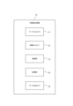
- 1 is a block diagram showing a configuration of a defect detection device according to an embodiment
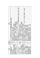
- FIG. 4 is a diagram illustrating defect detection parameters according to an embodiment.
- 3 is a diagram showing an area in which a defect detection device according to an embodiment detects defects
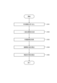
- 5 is a flowchart showing a detection process for protrusion defects by the defect detection device according to the embodiment.
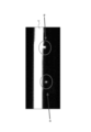
- 1A to 1C are diagrams illustrating an ROI image extraction process in the defect detection device according to an embodiment.
- FIG. 1 is a diagram showing an example of a protrusion defect and an isolated defect
- 5A to 5C are diagrams illustrating a binarization process and an inner circumference coordinate acquisition process in the defect detection device according to the embodiment.
- FIG. 5 is a flowchart showing a detection process for an isolated defect in the defect detection device according to the embodiment.
- 5A to 5C are diagrams illustrating a detection process of a first mask region in the defect detection device according to the embodiment.
- FIG. 13 is a diagram showing an example of a double ring image.
- 11A to 11C are diagrams illustrating a detection process of a second mask region in the defect detection device according to an embodiment.
- FIG. 4 is a diagram showing an invalid range of defect detection in the defect detection device according to the embodiment;
- Fig. 1 shows a wafer inspection apparatus according to an embodiment of the present invention.
- the wafer inspection apparatus 100 shown in Fig. 1 includes an optical system 30, a scanning unit 40, and a defect detection apparatus 50.
- the wafer inspection apparatus 100 is an apparatus that inspects the appearance of a wafer surface, including the front surface or back surface of the wafer.
- the wafer W is a silicon wafer or the like, and may be a polished wafer, an epitaxial wafer in which an epitaxial layer is formed on the front surface of a polished wafer, or a wafer in which a thin film such as a CVD (Chemical Vapor Deposition) film is formed on the back surface of an epitaxial wafer.
- the type of thin film may be, for example, an oxide film such as a silicon oxide film, or a nitride film such as a silicon nitride film.
- the scanning unit 40 scans the optical system 30 parallel to the surface of the wafer W.
- the scanning unit 40 may scan the optical system 30 in the circumferential direction, or vertically and horizontally.
- the wafer inspection device 100 may also have multiple optical systems 30 (e.g., three), and the scanning unit 40 may scan each optical system 30 in the circumferential direction.
- the scanning unit 40 may be composed of an arm connected to the optical system 30, and a drive stepping motor, servo motor, etc. for driving the arm.
- the optical system 30 has a ring fiber illumination 10 and an imaging unit 20.
- the optical system 30 is installed perpendicular to the front or back surface of the wafer W, and illuminates the front or back surface of the wafer W with the ring fiber illumination 10, and the scattered light is received by the imaging unit 20.
- Figure 1 shows how the back surface of the wafer W is illuminated by the optical system 30.
- the ring fiber light 10 illuminates the wafer W.
- a typical ring fiber light 10 can be used, and the illuminance of the illumination light L is, for example, about 100,000 to 1,000,000 lux.
- the angle that the illumination light L makes with respect to the wafer W is typical, for example, about 10 to 30 degrees.
- the configuration of the imaging unit 20 is not particularly limited as long as it can receive and capture scattered light from the wafer W.
- the imaging unit 20 includes a lens barrel 22, a lens 23, and a light receiving unit 24.
- the lens barrel 22, the lens 23, and the light receiving unit 24 can each be any commonly used component.
- the lens 23 can be, for example, a telecentric lens, and the light receiving unit 24 can be, for example, a CCD camera.
- the photographing unit 20 photographs the wafer surface by dividing it into multiple regions along the circumferential direction of the wafer W.
- the image photographed of each region is also called a shot image (part image).
- the photographing unit 20 may obtain the shot images by rotating the stage on which the wafer W is placed and photographing the rotating wafer W.
- the photographing unit 20 associates information specifying the relationship between the shot image and the position on the wafer surface where the shot image was photographed with the shot image, and outputs the information to the defect detection device 50.
- the defect detection device 50 shown in Fig. 2 includes a data input I/F (interface) 51, an image input I/F 52, a control unit 53, a storage unit 54, and a data output I/F 55.
- the defect detection device 50 may further include a communication I/F such as a LAN (Local Area Network) I/F to enable communication with an external device.
- a communication I/F such as a LAN (Local Area Network) I/F to enable communication with an external device.
- the data input I/F 51 is an interface between the defect detection device 50 and an input device, and the defect detection device 50 is connected to the input device via the data input I/F 51.
- the input device is a keyboard, a mouse, a pointing device, etc.
- the data input I/F 51 acquires parameters used for defect detection (defect detection parameters) from the input device and outputs them to the memory unit 54.
- the defect detection parameters may be set by the user using the input device.
- FIG. 3 shows an example of defect detection parameters.
- the defect detection parameters are used in the processing of the control unit 53. Therefore, the defect detection parameters shown in FIG. 3 will also be mentioned in the explanation of the control unit 53 described later. Furthermore, in this specification, the names of the defect detection parameters will be enclosed in "".
- the image input I/F 52 is an interface between the defect detection device 50 and the photographing unit 20, and the defect detection device 50 is connected to the photographing unit 20 via the image input I/F 52.
- the image input I/F 52 acquires an image of the wafer W photographed by the photographing unit 20.
- the image input I/F 52 outputs the photographed image to the memory unit 54. If the photographed image is analog data, the image input I/F 52 converts it into digital data. In this embodiment, the photographed image output by the image input I/F 52 is an 8-bit digital image.
- the storage unit 54 includes one or more memories, and may include, for example, a semiconductor memory, a magnetic memory, an optical memory, etc. Each memory included in the storage unit 54 may function, for example, as a main memory device, an auxiliary memory device, or a cache memory.
- the storage unit 54 stores any information used in the operation of the defect detection device 50. A portion of the storage unit 54 may be provided outside the defect detection device 50.
- the data output I/F 55 outputs the analysis results by the control unit 53 to a display device such as a display.
- the control unit 53 analyzes the captured image based on the defect detection parameters and detects defects.
- the control unit 53 may be configured with dedicated hardware such as an ASIC (Application Specific Integrated Circuit) or an FPGA (Field-Programmable Gate Array), or may be configured with a processor, or may be configured to include both.
- ASIC Application Specific Integrated Circuit
- FPGA Field-Programmable Gate Array
- FIG. 4 is a cross-sectional view of a wafer W, showing the edge region where defects are to be detected.
- the wafer W has a chamfered portion (bevel portion) BV on the front and back sides due to chamfering.
- the back side of the wafer W has been polished in a predetermined region (e.g., 500 to 600 ⁇ m) further inward from the chamfered portion BV, resulting in a polished surface (polished surface) P.
- the control unit 53 performs defect detection in a predetermined region (e.g., 1 mm) inward from the edge end face EF and in the polished surface (polished surface) P region.
- the inner side refers to the side facing toward the center of the wafer W (the direction of the arrow in the figure).
- FIG. 5 is a flowchart showing an example of the detection process of protrusion defects by the control unit 53.
- the control unit 53 inputs a shot image of the wafer W from the memory unit 54. Then, based on the defect detection parameters "ROI cut-out start position" and "ROI cut-out width", the control unit 53 cuts out a rectangular area including an edge ring image generated at the point where the polishing surface P contacts the boundary B from each shot image as an ROI (Region of Interest) image.
- the "ROI cut-out start position” is a parameter that indicates the cut-out start position of the ROI image in the shot image.
- the "ROI cut-out width” is a parameter that indicates the width to be cut out as the ROI image.
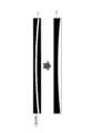
- FIG. 6 is a diagram for explaining the ROI image cutout process in step S101.
- an edge ring image E is displayed on the right side of a shot image of 640 ⁇ 480 pixels.
- the edge ring image E is displayed in white in the shot image because of its high brightness due to halation.
- the "ROI cutout start position” indicates the image coordinates in the X direction (horizontal direction) of the cutout start position of the ROI image with the upper left corner pixel of the shot image as the origin
- the "ROI cutout width” indicates the number of pixels in the X direction of the ROI image, with the "ROI cutout start position" being 566 and the "ROI cutout width” being 44.
- control unit 53 cuts out the ROI image with a width of 44 pixels from the 566th pixel in the X direction of the shot image as shown in FIG. 6.
- the image obtained by rotating the ROI image shown in FIG. 6 counterclockwise by 90 degrees is used as the ROI image.
- FIG. 7 shows an example of a pixel (protrusion defect) PD indicating a protrusion defect and a pixel (isolated defect) ID indicating an isolated defect in an image obtained by enlarging a portion of an ROI image.
- a protrusion defect PD is a pixel that is in contact with the inner circumference of the edge ring image E and has a high brightness value.
- a protrusion defect PD is displayed in white in the ROI image, protruding from the inner circumference of the edge ring image E.
- An isolated defect ID is a pixel inside the edge ring image E, separated from the inner circumference of the edge ring image E to the inside, and has a high brightness value.
- An isolated defect ID is displayed in white as an isolated blob in the ROI image.
- the control unit 53 binarizes the ROI image into a first value for higher brightness values and a second value for lower brightness values based on the defect detection parameter "protrusion defect detection threshold,” generating a binarized image.
- the "protrusion defect detection threshold” is a parameter that indicates the threshold when performing binarization processing for protrusion defect detection.
- step S103 the control unit 53 acquires, as the inner circumference coordinates, the image coordinates of the inner circumference of the area displayed by the first value in the binarized image.
- FIG. 8 is a diagram explaining the binarization process in step S102 and the inner circumference coordinate acquisition process in step S103.
- the "protrusion defect detection threshold" is 110.
- the control unit 53 converts pixels in the ROI image with a brightness value of 110 or more to a first value, and converts pixels in the ROI image with a brightness value of less than 110 to a second value.
- the first value is generally displayed in white
- the second value is generally displayed in black.
- control unit 53 scans the binarized image in the Y direction as shown in FIG. 8, and obtains the Y-direction image coordinates of the inner circumference I (indicated by the dashed line in the figure) where the color changes from white to black as the inner circumference coordinates.
- the unit of image coordinates is pixels.
- step S104 the control unit 53 performs differentiation processing on the inner circumference coordinates and calculates the change level of unevenness in the circumferential direction (X direction) as a coordinate differential value. For example, the difference value between inner circumference coordinates adjacent in the circumferential direction is calculated as the coordinate differential value.
- step S105 the control unit 53 detects protrusion defects by comparing the coordinate differential value with the "protrusion defect judgment level" of the defect detection parameters.
- the "protrusion defect judgment level” is a parameter that indicates the minimum coordinate differential value that is judged as a protrusion defect. For example, assume that the "protrusion defect judgment level” is 3. In this case, the control unit 53 detects as protrusion defects any location where the change level is 3 or greater.
- the control unit 53 may merge defects that exist within a range defined by the "grouping size" of the defect detection parameters as a single protrusion defect.
- the "grouping size” is a parameter that indicates the range to be merged. For example, assume that the "grouping size" indicates a central angle in units of 0.1 degrees and has a value of 15. In this case, the control unit 53 detects protrusion defects that exist within a sector-shaped range with a central angle of 1.5 degrees, with the center of the wafer W as the center of a circle, as a single protrusion defect.
- Figure 9 is a flowchart showing an example of the process of detecting isolated defects by the control unit 53.
- step S201 the control unit 53 cuts out the ROI image, similar to step S101.
- step S202 the control unit 53 binarizes the ROI image to generate a binarized image, similar to step S102.
- step S203 the control unit 53 detects the area in the binary image that is outside the inner circumference of the edge ring image (the side moving in the circumferential direction from the center of the wafer W) as the first mask area.
- the control unit 53 may enlarge the width between the outer and inner circumferences of the edge ring image based on the "mask enlargement size" of the defect detection parameters, and detect the area outside the inner circumference of the enlarged edge ring image as the first mask area.
- the "mask enlargement size" is a parameter that indicates the amount of enlargement of the width of the edge ring image.
- FIG. 10 is a diagram illustrating the detection process of the first mask region in step S203.
- the "mask enlargement size" is set to 2.
- the control unit 53 enlarges the width of the edge ring image E by two pixels toward the inner circumference (toward the bottom in this figure), and detects the area outside the inner circumference of the enlarged edge ring image (toward the top in this figure) as the first mask region M1.
- the first mask region M1 is shown in black.
- step S204 when the defect detection parameter "double ring removal” is enabled, the control unit 53 detects a double ring image from the ROI image based on the defect detection parameter "double ring determination threshold.”
- Double ring removal is a parameter indicating whether or not to perform double ring removal processing.
- Double ring determination threshold is a parameter indicating the threshold when performing double ring removal processing.
- double ring refers to a state in which the edge ring image E appears in the shape of double rings.
- FIG. 11 is a diagram showing an example of a double ring image.
- Double ring image D is an image that appears inside edge ring image E in the ROI image, and is an image made up of pixels whose brightness value is equal to or greater than the "double ring determination threshold.” For example, assume that "double ring removal” is enabled and the "double ring determination threshold" is 5. In this case, the control unit 53 detects pixels in the ROI image inside edge ring image E that have a brightness value of 5 or greater as double ring image D.
- step S205 the control unit 53 detects the area inside the outer periphery of the double ring image in the ROI image as the second mask area.
- FIG. 12 is a diagram illustrating the detection process of the second mask region in step S205.
- the control unit 53 detects the region in the ROI image that is inside the outer periphery of the double ring image D (the lower side in this figure) as the second mask region M2.
- the second mask region M2 is shown in black.
- the control unit 53 detects isolated defects in a judgment area obtained by excluding the first mask area and the second mask area from the ROI image, based on the defect detection parameter "threshold for detecting isolated defects.”
- the defect detection parameter "threshold for detecting isolated defects” is a parameter indicating the threshold when performing the binary processing for detecting isolated defects.
- the judgment area is the area sandwiched between the edge ring image (or the enlarged edge ring image if the width is enlarged) and the double ring image.
- the control unit 53 converts pixels in the judgment area with a brightness value of 50 or more to a first value, and converts pixels in the judgment area with a brightness value of less than 50 to a second value. Then, a cluster (blob) of pixels converted to the first value is detected as an isolated defect.
- step S206 if the blob is adjacent to a double ring image, the control unit 53 may determine that the blob is a double ring image and not detect the blob as an isolated defect.
- the control unit 53 may determine whether or not the blob is an isolated defect based on the defect detection parameter "double ring removal size.”
- the "double ring removal size” is a parameter that indicates the size of the blob when the blob is considered to be a double ring image. For example, assume that the "double ring removal size" is 100. In this case, if the number of pixels in the longitudinal direction of the blob is 100 or more, the control unit 53 determines that it is a double ring image and does not detect it as an isolated defect.
- control unit 53 The detection process for protrusion defects and isolated defects has been described above, but the processing of the control unit 53 is not limited to this. Other processing examples are shown below.
- the control unit 53 may determine the size (area) of protrusion defects and isolated defects based on the defect detection parameters "first defect size threshold” and "second defect size threshold".
- the "first defect size threshold” and “second defect size threshold” are parameters that indicate the classification of defect sizes. For example, the "first defect size threshold” is 5 and the “second defect size threshold” is 10. In this case, the control unit 53 determines that a defect with a pixel count of 5 or more and less than 10 is a first size defect. The control unit 53 also determines that a defect with a pixel count of 10 or more is a second size defect.
- the control unit 53 may obtain the number of first size defects, the number of second size defects, and the number of other sizes or the total number of defects, and display them on a display device via the data output I/F 55.
- the control unit 53 may also be configured not to detect protrusion defects and isolated defects in an edge region of the wafer W that is defined by the defect detection parameters "invalid range start position” and "invalid range end position.”
- the "invalid range start position” is a parameter that indicates the start position of a range (invalid range) in which protrusion defects and isolated defects are not detected
- the "invalid range end position” is a parameter that indicates the end position of the invalid range.
- a laser mark may be engraved on a part of the wafer W. In such a case, the laser mark can be excluded from the defect detection range using the "invalid range start position" and "invalid range end position.” The position of the laser mark is defined in SEMI standards T07 and M12.
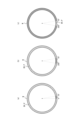
- FIG. 13 is a diagram showing an example of an invalid range for defect detection.
- the control unit 53 sets the invalid range to the range from 0 degrees to 10 degrees counterclockwise (central angle 10 degrees) with the notch position as the reference (0 degrees).
- the invalid range is shown with narrow diagonal lines, and the range of the chamfered portion BV and the polished surface P is shown with wide diagonal lines.
- FIG. 13(b) shows an invalid range when the "invalid range start position" is 350 and the "invalid range end position" is 10.
- the control unit 53 sets the invalid range to the range from 350 degrees to 10 degrees counterclockwise (central angle 20 degrees) with the notch position as 0 degrees.
- FIG. 13(c) shows an invalid range when the "invalid range start position" is 10 and the "invalid range end position” is 350.
- the control unit 53 sets the notch position to 0 degrees and sets the range from 10 degrees to 350 degrees counterclockwise (central angle 340 degrees) as the invalid range.
- the defect detection device 50 generates a binary image by binarizing the ROI image with a higher brightness value as a first value and a lower brightness value as a second value based on the "protrusion defect detection threshold", obtains the image coordinates of the inner circumference of the area displayed by the first value in the binary image as the inner circumference coordinate, calculates the change level of the unevenness in the circumferential direction of the inner circumference coordinate as a coordinate differential value, and compares the coordinate differential value with the "defect judgment level" to detect a protrusion defect.
- the defect detection device 50 detects an image that appears inside the edge ring image in the ROI image and is made up of pixels with a brightness value equal to or greater than the "double ring judgment threshold” as a double ring image, and detects a blob of pixels with a brightness value equal to or greater than the "isolated defect detection threshold” in the area between the edge ring image and the double ring image as an isolated defect.
- This method makes it possible to expand the defect detection area to the limit of halation that can be detected from the raw image.
- the detection of defects in edge regions was limited to a size of about 50 ⁇ m using visual inspection, the present invention makes it possible to detect defects as small as 0.2 ⁇ m with high sensitivity.
- a computer capable of executing program instructions may be used to function as the above-described defect detection apparatus 50.
- the computer may be a general-purpose computer, a dedicated computer, a workstation, a PC (Personal Computer), etc.
- the program instructions may be program code, code segments, etc. for performing the necessary tasks.
- the control unit 53 is a processor such as a CPU (Central Processing Unit), MPU (Micro Processing Unit), GPU (Graphics Processing Unit), DSP (Digital Signal Processor), or SoC (System on a Chip), and may be composed of multiple processors of the same or different types.
- the processor performs the above-mentioned processing by reading and executing a program from the memory unit 15. Note that at least a part of these processing contents may be realized by hardware.
- the program may be recorded on a computer-readable recording medium.
- the recording medium on which the program is recorded may be a non-transitory recording medium.
- Non-transitory recording media are not particularly limited, and may be, for example, a CD-ROM, a DVD-ROM, or a USB (Universal Serial Bus) memory.
- the program may be in a form that is downloaded from an external device via a network.
- the present invention can automatically detect defects with high sensitivity, making it useful for wafer inspection applications.
- Photography unit 22 Lens barrel 23
- Lens 24 Light receiving unit 30
- Optical system 40 Scanning unit 50 Defect detection device 51 Data input I/F 52 Image input I/F 53
- Control unit 54 Storage unit 55 Data output I/F 100 Wafer inspection device
Landscapes
- General Health & Medical Sciences (AREA)
- General Physics & Mathematics (AREA)
- Life Sciences & Earth Sciences (AREA)
- Chemical & Material Sciences (AREA)
- Analytical Chemistry (AREA)
- Biochemistry (AREA)
- Health & Medical Sciences (AREA)
- Immunology (AREA)
- Physics & Mathematics (AREA)
- Pathology (AREA)
- Engineering & Computer Science (AREA)
- Computer Vision & Pattern Recognition (AREA)
- Signal Processing (AREA)
- Testing Or Measuring Of Semiconductors Or The Like (AREA)
- Investigating Materials By The Use Of Optical Means Adapted For Particular Applications (AREA)
Abstract
Description
図1に、本発明の一実施形態に係るウェーハ検査装置を示す。図1に示すウェーハ検査装置100は、光学系30と、走査部40と、欠陥検出装置50と、を備える。ウェーハ検査装置100は、ウェーハの表面又は裏面を含むウェーハ面の外観を検査する装置である。
次に、図2を参照して、欠陥検出装置50の構成例を説明する。図2に示す欠陥検出装置50は、データ入力I/F(インターフェース)51と、画像入力I/F52と、制御部53と、記憶部54と、データ出力I/F55と、を備える。欠陥検出装置50は、外部の装置と通信可能とするために、LAN(Local Area Network)I/Fのような通信I/Fをさらに備えていてもよい。
次に、本発明における制御部53の処理を説明する。
上述した欠陥検出装置50として機能させるために、プログラム命令を実行可能なコンピュータを用いることも可能である。ここで、コンピュータは、汎用コンピュータ、専用コンピュータ、ワークステーション、PC(Personal Computer)などであってもよい。プログラム命令は、必要なタスクを実行するためのプログラムコード、コードセグメントなどであってもよい。
20 撮影部
22 鏡筒
23 レンズ
24 受光部
30 光学系
40 走査部
50 欠陥検出装置
51 データ入力I/F
52 画像入力I/F
53 制御部
54 記憶部
55 データ出力I/F
100 ウェーハ検査装置
Claims (9)
- 欠陥の検出に用いられるパラメータを取得するデータ入力I/Fと、
ウェーハの撮影画像を取得する画像入力I/Fと、
前記パラメータに基づいて前記撮影画像を解析し、前記ウェーハにおける欠陥を検出する制御部と、を備え、
前記パラメータは、突起状欠陥検出用閾値及び欠陥判定レベルを含み、
前記制御部は、
前記撮影画像から、前記ウェーハのエッジを示すエッジリング画像を含む矩形状の領域をROI画像として切り出し、
前記突起状欠陥検出用閾値に基づいて、前記ROI画像に対して輝度値が高い方を第1値、輝度値が低い方を第2値に二値化して二値化画像を生成し、
前記二値化画像における前記第1値で表示される領域の内周の画像座標を内周座標として取得し、
前記内周座標の周方向の凹凸の変化レベルを座標微分値として算出し、
前記座標微分値を前記欠陥判定レベルと比較することにより欠陥を検出する、欠陥検出装置。 - 前記パラメータは、グルーピングサイズを含み、
前記制御部は、前記グルーピングサイズによって規定される範囲内に存在する前記欠陥をまとめて1つの欠陥として検出する、請求項1に記載の欠陥検出装置。 - 欠陥の検出に用いられるパラメータを取得するデータ入力I/Fと、
ウェーハの撮影画像を取得する画像入力I/Fと、
前記パラメータに基づいて前記撮影画像を解析し、前記ウェーハにおける欠陥を検出する制御部と、を備え、
前記パラメータは、二重リング判定閾値及び孤立状欠陥検出用閾値を含み、
前記制御部は、
前記撮影画像から、前記ウェーハのエッジを示すエッジリング画像を含む矩形状の領域をROI画像として切り出し、
前記エッジリング画像の内側に現れる画像であって、輝度値が前記二重リング判定閾値以上の画素からなる画像を二重リング画像として検出し、
前記エッジリング画像と前記二重リング画像に挟まれた領域内において、輝度値が前記孤立状欠陥検出用閾値以上の画素のブロブを欠陥として検出する、欠陥検出装置。 - 前記パラメータは、マスク拡大サイズを含み、
前記制御部は、前記エッジリング画像の外周と内周の間の幅を前記マスク拡大サイズに基づいて拡大し、拡大後のエッジリング画像と前記二重リング画像に挟まれた領域内において、輝度値が前記孤立状欠陥検出用閾値以上の画素のブロブを前記欠陥として検出する、請求項3に記載の欠陥検出装置。 - 前記パラメータは、二重リング除去サイズを含み、
前記制御部は、前記ブロブの長手方向の画素数が前記二重リング除去サイズ以上の場合には前記欠陥として検出しない、請求項3に記載の欠陥検出装置。 - 前記パラメータは、無効範囲開始位置及び無効範囲終了位置を含み、
前記制御部は、前記ウェーハのエッジ領域のうち、前記無効範囲開始位置及び前記無効範囲終了位置によって規定される領域については前記欠陥の検出を行わない、請求項1又は3に記載の欠陥検出装置。 - 欠陥の検出に用いられるパラメータを取得するステップと、
ウェーハの撮影画像を取得するステップと、
前記パラメータに基づいて前記撮影画像を解析し、前記ウェーハにおける欠陥を検出する制御ステップと、を含み、
前記パラメータは、突起状欠陥検出用閾値及び欠陥判定レベルを含み、
前記制御ステップは、
前記撮影画像から、前記ウェーハのエッジを示すエッジリング画像を含む矩形状の領域をROI画像として切り出すステップと、
前記突起状欠陥検出用閾値に基づいて、前記ROI画像に対して輝度値が高い方を第1値、輝度値が低い方を第2値に二値化して二値化画像を生成するステップと、
前記二値化画像における前記第1値で表示される領域の内周の画像座標を内周座標として取得するステップと、
前記内周座標の周方向の凹凸の変化レベルを座標微分値として算出するステップと、
前記座標微分値を前記欠陥判定レベルと比較することにより、突起状の欠陥を検出するステップと、を含む、欠陥検出方法。 - 欠陥の検出に用いられるパラメータを取得するステップと、
ウェーハの撮影画像を取得するステップと、
前記パラメータに基づいて前記撮影画像を解析し、前記ウェーハにおける欠陥を検出する制御ステップと、を含み、
前記パラメータは、二重リング判定閾値及び孤立状欠陥検出用閾値を含み、
前記制御ステップは、
前記撮影画像から、前記ウェーハのエッジを示すエッジリング画像を含む矩形状の領域をROI画像として切り出すステップと、
前記エッジリング画像の内側に現れる画像であって、輝度値が前記二重リング判定閾値以上の画素からなる画像を二重リング画像として検出するステップと、
前記エッジリング画像と前記二重リング画像に挟まれた領域内において、輝度値が前記孤立状欠陥検出用閾値以上の画素のブロブを欠陥として検出するステップと、を含む、欠陥検出方法。 - コンピュータを、請求項1又は3に記載の欠陥検出装置として機能させるためのプログラム。
Priority Applications (3)
| Application Number | Priority Date | Filing Date | Title |
|---|---|---|---|
| KR1020257036470A KR20250168584A (ko) | 2023-06-09 | 2024-04-16 | 결함 검출 장치, 결함 검출 방법 및, 프로그램 |
| CN202480030334.5A CN121057936A (zh) | 2023-06-09 | 2024-04-16 | 缺陷检测装置、缺陷检测方法及程序 |
| DE112024002473.4T DE112024002473T5 (de) | 2023-06-09 | 2024-04-16 | Defektdetektionsvorrichtung, defektdetektionsverfahren und programm |
Applications Claiming Priority (2)
| Application Number | Priority Date | Filing Date | Title |
|---|---|---|---|
| JP2023-095846 | 2023-06-09 | ||
| JP2023095846A JP2024176947A (ja) | 2023-06-09 | 2023-06-09 | 欠陥検出装置、欠陥検出方法、及びプログラム |
Publications (1)
| Publication Number | Publication Date |
|---|---|
| WO2024252796A1 true WO2024252796A1 (ja) | 2024-12-12 |
Family
ID=93795386
Family Applications (1)
| Application Number | Title | Priority Date | Filing Date |
|---|---|---|---|
| PCT/JP2024/015191 Ceased WO2024252796A1 (ja) | 2023-06-09 | 2024-04-16 | 欠陥検出装置、欠陥検出方法、及びプログラム |
Country Status (6)
| Country | Link |
|---|---|
| JP (1) | JP2024176947A (ja) |
| KR (1) | KR20250168584A (ja) |
| CN (1) | CN121057936A (ja) |
| DE (1) | DE112024002473T5 (ja) |
| TW (1) | TWI903455B (ja) |
| WO (1) | WO2024252796A1 (ja) |
Citations (7)
| Publication number | Priority date | Publication date | Assignee | Title |
|---|---|---|---|---|
| US20040169869A1 (en) * | 2003-02-28 | 2004-09-02 | Koung-Su Shin | Method and apparatus for inspecting an edge exposure area of a wafer |
| WO2008139735A1 (ja) * | 2007-05-14 | 2008-11-20 | Nikon Corporation | 表面検査装置および表面検査方法 |
| JP2009042202A (ja) * | 2007-08-08 | 2009-02-26 | Taniguchi Consulting Engineers Co Ltd | ウエハ検査装置およびウエハ検査方法 |
| JP2010133841A (ja) * | 2008-12-05 | 2010-06-17 | Nikon Corp | 周部検査装置 |
| JP2013238595A (ja) * | 2012-05-11 | 2013-11-28 | Kla-Encor Corp | ウェーハジオメトリ計測ツールによるウェーハ表面フィーチャの検出、分類および定量化のためのシステムおよび方法 |
| JP2014095578A (ja) * | 2012-11-08 | 2014-05-22 | Hitachi High-Technologies Corp | 欠陥検出方法及びその装置並びに欠陥観察方法及びその装置 |
| JP2018146482A (ja) * | 2017-03-08 | 2018-09-20 | 株式会社Sumco | エピタキシャルウェーハの裏面検査方法、エピタキシャルウェーハ裏面検査装置、エピタキシャル成長装置のリフトピン管理方法およびエピタキシャルウェーハの製造方法 |
Family Cites Families (5)
| Publication number | Priority date | Publication date | Assignee | Title |
|---|---|---|---|---|
| JP5433201B2 (ja) | 2008-10-23 | 2014-03-05 | 株式会社Sumco | ウェーハ裏面の評価方法 |
| JP6531579B2 (ja) * | 2015-09-10 | 2019-06-19 | 株式会社Sumco | ウェーハ検査方法およびウェーハ検査装置 |
| JP6507967B2 (ja) | 2015-09-24 | 2019-05-08 | 株式会社Sumco | エピタキシャルウェーハ表面検査装置およびそれを用いたエピタキシャルウェーハ表面検査方法 |
| JP6601119B2 (ja) | 2015-10-05 | 2019-11-06 | 株式会社Sumco | エピタキシャルウェーハ裏面検査装置およびそれを用いたエピタキシャルウェーハ裏面検査方法 |
| JP7514677B2 (ja) * | 2020-07-13 | 2024-07-11 | 株式会社ニューフレアテクノロジー | パターン検査装置及びパターンの輪郭位置取得方法 |
-
2023
- 2023-06-09 JP JP2023095846A patent/JP2024176947A/ja active Pending
-
2024
- 2024-04-10 TW TW113113302A patent/TWI903455B/zh active
- 2024-04-16 DE DE112024002473.4T patent/DE112024002473T5/de active Pending
- 2024-04-16 CN CN202480030334.5A patent/CN121057936A/zh active Pending
- 2024-04-16 KR KR1020257036470A patent/KR20250168584A/ko active Pending
- 2024-04-16 WO PCT/JP2024/015191 patent/WO2024252796A1/ja not_active Ceased
Patent Citations (7)
| Publication number | Priority date | Publication date | Assignee | Title |
|---|---|---|---|---|
| US20040169869A1 (en) * | 2003-02-28 | 2004-09-02 | Koung-Su Shin | Method and apparatus for inspecting an edge exposure area of a wafer |
| WO2008139735A1 (ja) * | 2007-05-14 | 2008-11-20 | Nikon Corporation | 表面検査装置および表面検査方法 |
| JP2009042202A (ja) * | 2007-08-08 | 2009-02-26 | Taniguchi Consulting Engineers Co Ltd | ウエハ検査装置およびウエハ検査方法 |
| JP2010133841A (ja) * | 2008-12-05 | 2010-06-17 | Nikon Corp | 周部検査装置 |
| JP2013238595A (ja) * | 2012-05-11 | 2013-11-28 | Kla-Encor Corp | ウェーハジオメトリ計測ツールによるウェーハ表面フィーチャの検出、分類および定量化のためのシステムおよび方法 |
| JP2014095578A (ja) * | 2012-11-08 | 2014-05-22 | Hitachi High-Technologies Corp | 欠陥検出方法及びその装置並びに欠陥観察方法及びその装置 |
| JP2018146482A (ja) * | 2017-03-08 | 2018-09-20 | 株式会社Sumco | エピタキシャルウェーハの裏面検査方法、エピタキシャルウェーハ裏面検査装置、エピタキシャル成長装置のリフトピン管理方法およびエピタキシャルウェーハの製造方法 |
Also Published As
| Publication number | Publication date |
|---|---|
| JP2024176947A (ja) | 2024-12-19 |
| TW202501655A (zh) | 2025-01-01 |
| CN121057936A (zh) | 2025-12-02 |
| TWI903455B (zh) | 2025-11-01 |
| DE112024002473T5 (de) | 2026-04-16 |
| KR20250168584A (ko) | 2025-12-02 |
Similar Documents
| Publication | Publication Date | Title |
|---|---|---|
| TWI648534B (zh) | 磊晶晶圓之裏面檢查方法、磊晶晶圓裏面檢查裝置、磊晶成長裝置之升降銷管理方法以及磊晶晶圓之製造方法 | |
| JP3826849B2 (ja) | 欠陥検査方法および欠陥検査装置 | |
| JP2003215060A (ja) | パターン検査方法及び検査装置 | |
| CN108139339B (zh) | 外延晶片背面检查装置及使用其的外延晶片背面检查方法 | |
| JP2015511310A (ja) | ウエハ検査のためのセグメント化 | |
| JP2007071586A (ja) | 画像欠陥検査装置、画像欠陥検査システム、欠陥分類装置及び画像欠陥検査方法 | |
| JP6705338B2 (ja) | ウエハの異常を検査する装置及びその検査方法 | |
| TW202238112A (zh) | 晶圓表面缺陷檢測方法及其裝置 | |
| TWI843894B (zh) | 用於半導體晶圓檢測之系統及方法,及電腦可讀儲存媒體 | |
| KR102853085B1 (ko) | 기판 불량 검출 방법 및 장치 | |
| JP5917492B2 (ja) | 外観検査方法およびその装置 | |
| JP2009097928A (ja) | 欠陥検査装置及び欠陥検査方法 | |
| JP6259634B2 (ja) | 検査装置 | |
| WO2024252796A1 (ja) | 欠陥検出装置、欠陥検出方法、及びプログラム | |
| JP6628185B2 (ja) | 透明体の検査方法 | |
| CN112666175B (zh) | 异物检查装置和异物检查方法 | |
| JP2017058190A (ja) | 参照画像作成用の基準データ作成方法及びパターン検査装置 | |
| JP2014211417A (ja) | パターン検査装置及びパターン検査方法 | |
| JP3803677B2 (ja) | 欠陥分類装置及び欠陥分類方法 | |
| JP2006050356A (ja) | 画像処理方法及び検査装置 | |
| JPH07301609A (ja) | 欠陥検査方法 | |
| TW202536401A (zh) | 外觀檢查裝置及外觀檢查方法 | |
| JP2010243214A (ja) | 欠陥検出方法および欠陥検出装置 | |
| TW202601551A (zh) | 用於半導體裝置檢測的深度影像產生方法及深度影像產生系統 | |
| WO2024204649A1 (ja) | ウエハ検査装置、ウエハ検査システム、ウエハ検査方法、及びプログラム |
Legal Events
| Date | Code | Title | Description |
|---|---|---|---|
| 121 | Ep: the epo has been informed by wipo that ep was designated in this application |
Ref document number: 24819034 Country of ref document: EP Kind code of ref document: A1 |
|
| ENP | Entry into the national phase |
Ref document number: 1020257036470 Country of ref document: KR Free format text: ST27 STATUS EVENT CODE: A-0-1-A10-A15-NAP-PA0105 (AS PROVIDED BY THE NATIONAL OFFICE) |
|
| WWE | Wipo information: entry into national phase |
Ref document number: KR1020257036470 Country of ref document: KR |
|
| WWE | Wipo information: entry into national phase |
Ref document number: 112024002473 Country of ref document: DE |