WO2024252736A1 - 電子部品 - Google Patents
電子部品 Download PDFInfo
- Publication number
- WO2024252736A1 WO2024252736A1 PCT/JP2024/005976 JP2024005976W WO2024252736A1 WO 2024252736 A1 WO2024252736 A1 WO 2024252736A1 JP 2024005976 W JP2024005976 W JP 2024005976W WO 2024252736 A1 WO2024252736 A1 WO 2024252736A1
- Authority
- WO
- WIPO (PCT)
- Prior art keywords
- electrode
- electrodes
- electronic component
- insulator
- dummy
- Prior art date
- Legal status (The legal status is an assumption and is not a legal conclusion. Google has not performed a legal analysis and makes no representation as to the accuracy of the status listed.)
- Pending
Links
Images


Classifications
-
- H—ELECTRICITY
- H01—ELECTRIC ELEMENTS
- H01F—MAGNETS; INDUCTANCES; TRANSFORMERS; SELECTION OF MATERIALS FOR THEIR MAGNETIC PROPERTIES
- H01F27/00—Details of transformers or inductances, in general
-
- H—ELECTRICITY
- H01—ELECTRIC ELEMENTS
- H01F—MAGNETS; INDUCTANCES; TRANSFORMERS; SELECTION OF MATERIALS FOR THEIR MAGNETIC PROPERTIES
- H01F27/00—Details of transformers or inductances, in general
- H01F27/28—Coils; Windings; Conductive connections
- H01F27/29—Terminals; Tapping arrangements for signal inductances
-
- H—ELECTRICITY
- H01—ELECTRIC ELEMENTS
- H01G—CAPACITORS; CAPACITORS, RECTIFIERS, DETECTORS, SWITCHING DEVICES, LIGHT-SENSITIVE OR TEMPERATURE-SENSITIVE DEVICES OF THE ELECTROLYTIC TYPE
- H01G4/00—Fixed capacitors; Processes of their manufacture
- H01G4/30—Stacked capacitors
-
- H—ELECTRICITY
- H01—ELECTRIC ELEMENTS
- H01G—CAPACITORS; CAPACITORS, RECTIFIERS, DETECTORS, SWITCHING DEVICES, LIGHT-SENSITIVE OR TEMPERATURE-SENSITIVE DEVICES OF THE ELECTROLYTIC TYPE
- H01G4/00—Fixed capacitors; Processes of their manufacture
- H01G4/40—Structural combinations of fixed capacitors with other electric elements, the structure mainly consisting of a capacitor, e.g. RC combinations
Definitions
- This disclosure relates to an electronic component that has an external electrode on the side of an insulator.
- Patent Document 1 discloses the configuration of an electronic component that prevents moisture from penetrating.
- Patent Document 1 JP 2004-273917 A (Patent Document 1), a protruding convex portion is formed on the side edge of the pull-out portion of the internal electrode to prevent moisture from penetrating from the end face of the electronic component along the vicinity of the side edge of the pull-out portion.
- a convex portion on the internal electrode cannot prevent problems such as migration that occur between the internal electrode and the side electrode that is electrically connected to the external electrode.
- the purpose of this disclosure is to provide electronic components that can suppress the occurrence of defects such as migration.
- An electronic component includes an insulator formed by stacking a plurality of insulating substrates, each of which includes a side electrode and an internal electrode, and an external electrode electrically connected to the side electrode and provided on a side surface of the insulator.
- Each of the plurality of insulating substrates further includes dummy electrodes disposed on both sides of the side electrode with an insulating portion sandwiched therebetween when viewed from the stacking direction.
- the external electrodes are connected to the dummy electrodes on the side surfaces of the insulator.
- the insulating substrates further include dummy electrodes arranged on both sides of the side electrodes with insulating portions sandwiched therebetween when viewed from the stacking direction, thereby making it possible to suppress the occurrence of defects such as migration.
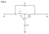
- FIG. 1 is a perspective view of an electronic component according to an embodiment; 1 is a circuit diagram of an electronic component according to an embodiment. 2 is a plan view of the vicinity of one external electrode of the electronic component according to the embodiment. FIG. 2 is a cross-sectional view of the vicinity of one external electrode of the electronic component according to the embodiment.
- FIG. 1 is an exploded plan view illustrating a configuration of an electronic component according to an embodiment.
- FIG. 13 is an exploded plan view showing a configuration of an electronic component according to a first modified example.
- FIG. 11 is an exploded plan view showing a configuration of an electronic component according to a second modified example.
- FIG. 11 is a plan view of the vicinity of one external electrode of an electronic component according to Modification 3.
- a filter circuit including a coil and a capacitor is formed with internal electrodes within a rectangular parallelepiped insulator.
- the filter circuit does not need to be formed with internal electrodes, and other circuits may be formed with internal electrodes.
- Fig. 1 is a perspective view of an electronic component 1 according to an embodiment.
- Fig. 2 is a circuit diagram of the electronic component 1 according to an embodiment.
- the short side direction of the electronic component 1 is the X direction
- the long side direction is the Y direction
- the height direction is the Z direction.
- the stacking direction of the insulating substrate (hereinafter also simply referred to as substrate) is the Z direction
- the direction of the arrow indicates the upper layer direction.
- Electronic component 1 is a filter circuit in which a first coil L1 and a second coil L2 that constitute a transformer are arranged in the stacking direction, and a first capacitor C1 and a second capacitor C2 are arranged in the Y direction.
- the electronic component 1 has a first coil L1 and a second coil L2 that are magnetically coupled and connected in series between a first terminal P1 and a second terminal P2. Furthermore, the electronic component 1 has a first capacitor C1 connected in parallel to the first coil L1 and the second coil L2, and an intermediate terminal between the first coil L1 and the second coil L2 is connected to ground (GND) via a second capacitor C2.
- GND ground
- the electronic component 1 is composed of an insulator 3 formed by stacking multiple substrates on which internal electrodes that form part of a coil and part of a capacitor are formed. Side electrodes that form the first terminal P1, second terminal P2, GND terminal, and free terminal (NC terminal) are formed at the four corners of the substrate.
- the insulator 3 may be manufactured using a method of forming an electrode pattern of the internal electrodes and side electrodes with a photomask that uses a photosensitive conductive paste and a photosensitive insulating paste.
- the insulator 3 may also be manufactured using a method of stacking ceramic green sheets, which are insulating substrates, using a process of forming an electrode pattern by screen printing, or a process of drilling holes in an insulating layer with a laser and filling them with via electrodes.
- the insulator 3 has a pair of first and second principal surfaces that face each other, and a side surface that connects the first and second principal surfaces. As shown in FIG. 1, the insulator 3 is made up of substrates stacked in the Z direction on which the internal electrode 11 of the first coil L1, the internal electrode 12 of the second coil L2, the internal electrode 13 of the first capacitor C1, and the internal electrode 14 of the second capacitor C2 that constitute the filter circuit are formed.
- the four corners of the insulator 3 are formed with a side electrode 21 constituting the first terminal P1, a side electrode 22 constituting the second terminal P2, a side electrode 23 constituting the GND terminal, and a side electrode 24 constituting the vacant terminal (NC terminal).
- the shape of the external electrodes 41 to 44 when viewed from the stacking direction is a rectangle. Note that the side electrodes 21 to 24 do not need to be formed at the four corners of the insulator 3, but only need to be formed on the outer periphery of the insulator 3.
- the side electrodes 21 to 24 formed on the outer periphery of the insulator 3 are electrically connected to the external electrodes 41 to 44 formed on the side surfaces of the insulator 3, respectively.
- the external electrodes 41 to 44 may be formed not only on the side surfaces of the insulator 3, but also on the bottom surface (second main surface) of the insulator 3 as shown in FIG. 1. Of course, the external electrodes 41 to 44 may be formed not only on the bottom surface (second main surface) of the insulator 3, but also on the top surface (first main surface) of the insulator 3.
- the external electrodes 41 to 44 are thin film layers formed on the side and bottom surfaces of the insulator 3, and are plating layers. For example, if the side electrodes 21 to 24 are formed from silver (Ag) paste, the external electrodes 41 to 44 are formed from a gold (Au) plating layer to make it easier to solder the electronic component 1 to the mounting board.
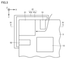
- FIG. 3 is a plan view of the vicinity of one external electrode 41 of an electronic component 1 according to an embodiment.
- an external electrode 41 including a nickel (Ni) plating layer 41a (first external electrode layer) and a gold (Au) plating layer 41b (second external electrode layer) is provided on the side of the insulator 3 on which the side electrode 21 is formed.
- a gap may occur at the interface between the side of the insulator 3 and the external electrode 41.
- the nickel (Ni) plating layer 41a may be dissolved (Ni corrosion) when the gold (Au) plating layer 41b is formed, so a gap occurs at the interface between the side of the insulator 3 and the external electrode 41. If a gap occurs at the interface between the side of the insulator 3 and the external electrode 41, moisture may penetrate into the insulator 3 through the gap, causing problems such as migration.
- dummy electrodes 51 and 52 are provided on both sides of the side electrode 21, sandwiching an insulating portion, when viewed from the stacking direction (Z direction). Note that the dummy electrodes are omitted from the electronic component 1 shown in FIG. 1. Also, in FIG. 3, the gaps occurring at the interface between the side of the insulator 3 and the external electrode 41 are shown by dashed triangles, and the moisture penetrating through the gaps is shown by arrows.
- the dummy electrode 51 the moisture penetrating through the gaps cannot reach the side electrode 21 without bypassing the dummy electrode 51, and the occurrence of defects such as migration occurring between the side electrode 21 and the internal electrode 13 can be suppressed.
- the dummy electrodes 51 and 52 the path from the end of the external electrode 41 to the side electrode 21 can be extended, and the penetration path of moisture penetrating into the inside of the insulator 3 can be lengthened.
- the external electrode 41 is provided from the side electrode 21 to the position where the dummy electrodes 51, 52 are arranged, and is connected to the dummy electrodes 51, 52 on the side of the insulator 3. In other words, the external electrode 41 is connected not only to the side electrode 21 but also to the dummy electrodes 51, 52. If the insulator 3 is formed of, for example, a glass element, the side electrode 21 and the dummy electrodes 51, 52 have a higher degree of adhesion to the external electrode 41, which is a plating layer, than the glass element.
- the dummy electrodes 51, 52 are formed of the same material as the side electrode 21, for example, a silver (Ag) paste, but may be made of a different material from the side electrode 21 as long as the material has a higher degree of adhesion to the external electrode 41 than the glass element.
- the dummy electrodes 51, 52 are made of the same material as the side electrode 21, then even if the area of the side electrode 21 is reduced by providing the dummy electrodes 51, 52, it is possible to suppress a decrease in the degree of adhesion between the external electrode 41 and the insulator 3. Furthermore, when the insulator 3 is fired, a stress that peels off the side electrode 21 from the insulator 3 occurs due to the difference in thermal contraction rate between the glass element insulator 3 and the metal side electrode 21. However, by providing the dummy electrodes 51, 52, the area of the side electrode 21 is reduced, thereby alleviating the peeling stress and suppressing the occurrence of delamination.
- the shape of the dummy electrodes 51, 52 when viewed from the stacking direction (Z direction) is preferably rectangular in which the side not in contact with the external electrode 41 is longer than the side in contact with the external electrode 41. This ensures a sufficient peripheral length for the dummy electrodes 51, 52.
- the shape of the dummy electrodes 51, 52 is not limited to a rectangular shape, and may be a triangle, a circle, a polygon, etc.
- the distance between the dummy electrodes 51, 52 and the internal electrode 13 is longer than the distance between the side electrode 21 and the internal electrode 13. This can prevent the creation of a path for moisture to penetrate from the dummy electrodes 51, 52 to the internal electrode 13.
- the distance here means the shortest distance connecting the side electrode 21 and the internal electrode 13.
- FIG. 4 is a cross-sectional view of the vicinity of one external electrode 41 of the electronic component 1 according to the embodiment.
- the cross-sectional view shown in FIG. 4 is a cross-sectional view of the IV-IV surface of FIG. 3. Note that the electronic component 1 shown in FIG. 4 differs from the electronic component 1 shown in FIG. 1 in that an external electrode 41 is also provided on the top surface of the insulator 3.
- the side electrode 21a first side electrode
- the side electrode 21b second side electrode one layer closer to the bottom surface of the insulator 3 than the side electrode 21a are not electrically connected by a via conductor. Note that this is not limited to the case where the side electrode 21b is provided one layer below the side electrode 21a, and at least one layer of insulating substrate on which no side electrode or internal electrode is formed may be sandwiched between the side electrodes 21a and 21b. In other words, it is sufficient that the side electrode 21b is adjacent to the side electrode 21a at a position closer to the bottom surface of the insulator 3 than the side electrode 21a.
- the side electrode 21a is not connected to the side electrode 21b by a via conductor, so the penetrated moisture cannot reach the side electrode 21b without bypassing the side electrode 21a, and it is possible to suppress the occurrence of defects such as migration between the side electrode 21b and the internal electrode.
- the side electrode 21a and the side electrode 21b by not connecting the side electrode 21a and the side electrode 21b by a via conductor, it is possible to extend the path from the end of the external electrode 41 to the side electrode 21b, and it is possible to lengthen the penetration path of moisture that penetrates into the inside of the insulator 3.
- the dummy electrode 51a provided in the same layer as the side electrode 21a also contributes to lengthening the penetration path of moisture that penetrates into the inside of the insulator 3.
- the side electrode 21k third side electrode
- the side electrode 21j fourth side electrode one layer closer to the top surface of the insulator 3 than the side electrode 21k are not electrically connected by a via conductor. Note that this is not limited to the case where the side electrode 21j is provided one layer above the side electrode 21k, and at least one layer of insulating substrate on which no side electrode or internal electrode is formed may be sandwiched between the side electrode 21k and the side electrode 21j.
- the side electrode 21j is adjacent to the side electrode 21k at a position closer to the top surface of the insulator 3 than the side electrode 21k. Therefore, the path from the end of the external electrode 41 to the side electrode 21j can be extended, and the path of moisture penetrating into the inside of the insulator 3 can be lengthened.
- the dummy electrode 51k which is provided in the same layer as the side electrode 21k, also contributes to lengthening the path through which moisture penetrates into the inside of the insulator 3.
- the side electrodes of each layer are electrically connected to each other by via conductors, except between side electrode 21a and side electrode 21b, and between side electrode 21k and side electrode 21j.
- side electrode 21b and side electrode 21c are electrically connected to each other by via conductor 31
- side electrode 21c and side electrode 21d are electrically connected to each other by via conductor 32. Note that this is not limited to the case where all side electrodes of each layer are electrically connected to each other by via conductors, except between side electrode 21a and side electrode 21b, and between side electrode 21k and side electrode 21j, as long as the side electrodes of some layers are electrically connected to each other by via conductors. Of course, it is not necessary that the side electrodes of all layers are electrically connected to each other by via conductors.
- the via conductors (e.g., via conductors 31, 32) that connect the side electrodes of each layer to each other are preferably electrically connected directly to the external electrode 41.
- the electrical resistance between the external electrode 41 and the side electrode can be kept low.
- the electrical resistance is low, it is not necessary to electrically connect the via conductors (e.g., via conductors 31, 32) that connect the side electrodes of each layer to each other to the external electrode 41 directly.
- the configuration near the external electrode 41 has been described in Figures 3 and 4, but the electronic component 1 also employs a similar configuration near the other external electrodes 42 to 44, making it possible to suppress problems such as migration between the side electrodes and the internal electrodes.
- the electronic component 1 employs dummy electrodes 51 and 52 shown in Figure 3, but does not necessarily have to employ the configuration shown in Figure 4.
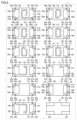
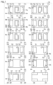
- FIG. 5 is an exploded plan view showing the configuration of an electronic component 1 according to an embodiment.
- each of the electrode patterns of the internal electrodes and side electrodes of the coils and capacitors are formed with conductive paste (Ag paste) on insulating substrates 3a to 3l, which are the substrates, as shown in FIG. 5.
- conductive paste Ag paste
- the insulating substrate 3a is formed with side electrodes 21a to 24a and dummy electrodes 51a to 58a. Furthermore, the insulating substrate 3a is formed with an internal electrode 12a that constitutes part of the second coil L2, an internal electrode 13a that constitutes part of the first capacitor C1, and an internal electrode 14a that constitutes part of the second capacitor C2. The internal electrode 12a is electrically connected to the internal electrode 13a.
- Insulating substrate 3b has side electrodes 21b to 24b and dummy electrodes 51b to 58b formed thereon. Furthermore, insulating substrate 3b has internal electrode 12b forming part of second coil L2, internal electrode 13b forming part of first capacitor C1, and internal electrode 14b forming part of second capacitor C2 formed thereon. Side electrode 21b is electrically connected to internal electrode 13b, and side electrode 24b is electrically connected to internal electrode 14b. Furthermore, connection point 34b of side electrode 22b is electrically connected to connection point 34a of internal electrode 13a via via conductor 34. Connection point 33b of side electrode 23b is electrically connected to connection point 33a of internal electrode 14a via via conductor 33.
- Insulating substrate 3c has side electrodes 21c to 24c and dummy electrodes 51c to 58c formed thereon. Furthermore, insulating substrate 3c has internal electrode 12c forming part of second coil L2, internal electrode 13c forming part of first capacitor C1, and internal electrode 14c forming part of second capacitor C2 formed thereon. Side electrode 22c is electrically connected to internal electrode 13c, and side electrode 23c is electrically connected to internal electrode 14c.
- Insulating substrate 3d has side electrodes 21d to 24d and dummy electrodes 51d to 58d formed thereon. Furthermore, insulating substrate 3d has internal electrode 12d forming part of second coil L2, internal electrode 13d forming part of first capacitor C1, and internal electrode 14d forming part of second capacitor C2 formed thereon. Side electrode 21d is electrically connected to internal electrode 13d, and side electrode 24d is electrically connected to internal electrode 14d. Furthermore, internal electrode 12d is electrically connected to internal electrode 14d. Internal electrodes 12a to 12d are electrically connected by via conductors (not shown) to form second coil L2.
- Insulating substrate 3e has side electrodes 21e to 24e and dummy electrodes 51e to 58e formed thereon. Furthermore, insulating substrate 3e has internal electrode 13e that constitutes part of first capacitor C1 and internal electrode 14e that constitutes part of second capacitor C2 formed thereon. Side electrode 22e is electrically connected to internal electrode 13e, and side electrode 23e is electrically connected to internal electrode 14e.
- Insulating substrate 3f is formed with side electrodes 21f to 24f and dummy electrodes 51f to 58f. Furthermore, insulating substrate 3f is formed with internal electrode 11f constituting part of first coil L1, internal electrode 13f constituting part of first capacitor C1, and internal electrode 14f constituting part of second capacitor C2. Side electrode 21f is electrically connected to internal electrode 13f, and side electrode 24f is electrically connected to internal electrode 14f. Furthermore, internal electrode 11f is electrically connected to internal electrode 14f.
- Insulating substrate 3g is formed with side electrodes 21g to 24g and dummy electrodes 51g to 58g. Furthermore, insulating substrate 3g is formed with internal electrode 11g that constitutes part of first coil L1, internal electrode 13g that constitutes part of first capacitor C1, and internal electrode 14g that constitutes part of second capacitor C2. Side electrode 22g is electrically connected to internal electrode 13g, and side electrode 23g is electrically connected to internal electrode 14g.
- Insulating substrate 3h has side electrodes 21h to 24h and dummy electrodes 51h to 58h formed thereon. Furthermore, insulating substrate 3h has internal electrode 11h that constitutes part of first coil L1, internal electrode 13h that constitutes part of first capacitor C1, and internal electrode 14h that constitutes part of second capacitor C2 formed thereon. Side electrode 21h is electrically connected to internal electrode 13h, and side electrode 24h is electrically connected to internal electrode 14h.
- Insulating substrate 3i is formed with side electrodes 21i to 24i and dummy electrodes 51i to 58i. Furthermore, insulating substrate 3i is formed with internal electrode 11i that constitutes part of first coil L1, internal electrode 13i that constitutes part of first capacitor C1, and internal electrode 14i that constitutes part of second capacitor C2. Side electrode 22i is electrically connected to internal electrode 13i, and side electrode 23i is electrically connected to internal electrode 14i.
- Insulating substrate 3j has side electrodes 21j to 24j and dummy electrodes 51j to 58j formed thereon. Furthermore, insulating substrate 3j has internal electrode 11j forming part of first coil L1, internal electrode 13j forming part of first capacitor C1, and internal electrode 14j forming part of second capacitor C2 formed thereon. Side electrode 21j is electrically connected to internal electrode 13j, and side electrode 24j is electrically connected to internal electrode 14j. Furthermore, internal electrode 11j is electrically connected to internal electrode 13j. Internal electrodes 11f to 11j are electrically connected by via conductors (not shown) to form first coil L1.
- Insulating substrate 3k has side electrodes 21k to 24k and dummy electrodes 51k to 58k formed thereon. Furthermore, insulating substrate 3k has internal electrode 13k forming part of first capacitor C1 and internal electrode 14k forming part of second capacitor C2 formed thereon. Connection point 36k of internal electrode 13k is electrically connected to connection point 36j of side electrode 22j through via conductor 36. Connection point 35k of internal electrode 14k is electrically connected to connection point 35j of side electrode 23j through via conductor 35.
- the insulating substrate 3l has side electrodes 21l to 24l formed in correspondence with the external electrodes 41 to 44 formed on the bottom surface of the insulator 3.
- dummy electrodes 51a to 51k are collectively referred to as dummy electrode 51
- dummy electrodes 52a to 52k are collectively referred to as dummy electrode 52
- dummy electrodes 53a to 53k are collectively referred to as dummy electrode 53
- dummy electrodes 54a to 54k are collectively referred to as dummy electrode 54.
- dummy electrodes 55a to 55k are collectively referred to as dummy electrode 55
- dummy electrodes 56a to 56k are collectively referred to as dummy electrode 56
- dummy electrodes 57a to 57k are collectively referred to as dummy electrode 57
- dummy electrodes 58a to 58k are collectively referred to as dummy electrode 58.
- At least one of the insulating substrates 3a to 3l shown in FIG. 5 is laminated, and multiple insulating substrates (dummy layers) without electrode patterns printed on both the top and bottom sides are laminated.
- the multiple insulating substrates, including the dummy layers, are pressed together to form an unfired insulator 3 (glass element).
- the formed insulator 3 is fired, and the external electrodes 41 to 44 are formed on the outside of the fired insulator 3 by plating.
- the electronic component 1 includes an insulator 3 formed by stacking a plurality of insulating substrates, each of which includes side electrodes 21-24 and internal electrodes 11-14, and external electrodes 41-44 electrically connected to the side electrodes 21-24 and provided on the side of the insulator 3.
- Each of the plurality of insulating substrates 3a-3k further includes dummy electrodes 51-58 arranged on both sides of the side electrodes 21-24 with an insulating portion sandwiched between them when viewed from the stacking direction.
- the external electrodes 41-44 are provided from the side electrodes 21-24 to the positions where the dummy electrodes 51-58 are arranged, and are connected to the dummy electrodes 51-58 on the side of the insulator 3.
- the multiple insulating substrates further include dummy electrodes 51-58 arranged on both sides of the side electrodes 21-24, sandwiching an insulating portion, when viewed from the stacking direction, thereby suppressing the occurrence of defects such as migration.
- the internal electrodes 13a, 14a closest to the top surface of the insulator 3 and the internal electrodes 13k, 14k closest to the bottom surface of the insulator 3 are not electrically connected to the side electrodes.
- this is not limited to the above, and the internal electrodes 13a, 14a and the internal electrodes 13k, 14k may be electrically connected to the side electrodes.
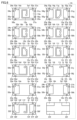
- FIG. 6 is an exploded plan view showing the configuration of electronic component 1A according to modified example 1. Note that in the configuration of electronic component 1A according to modified example 1, the same components as those in electronic component 1 according to the embodiment are given the same reference numerals and detailed descriptions will not be repeated.
- the insulating substrate 3a1 is formed with side electrodes 21a to 24a and dummy electrodes 51a to 58a. Furthermore, the insulating substrate 3a1 is formed with an internal electrode 12a constituting a part of the second coil L2, an internal electrode 13a constituting a part of the first capacitor C1, and an internal electrode 14a constituting a part of the second capacitor C2.
- the internal electrode 13a is electrically connected to the side electrode 22a
- the internal electrode 14a is electrically connected to the side electrode 23a. Therefore, even if the via conductor 33 is not provided, the internal electrode 14a is electrically connected to the side electrode 23b because the side electrodes 23a and 23b are electrically connected through the external electrode 43 (see FIG. 1). Also, even if the via conductor 34 is not provided, the internal electrode 13a is electrically connected to the side electrode 22b because the side electrodes 22a and 22b are electrically connected through the external electrode 42 (see FIG. 1).
- Insulating substrate 3k1 has side electrodes 21k to 24k and dummy electrodes 51k to 58k formed thereon.
- insulating substrate 3k1 has internal electrode 13k forming part of first capacitor C1 and internal electrode 14k forming part of second capacitor C2 formed thereon.
- Internal electrode 13k is electrically connected to side electrode 22k
- internal electrode 14k is electrically connected to side electrode 23k. Therefore, even without via conductor 35, internal electrode 14k is electrically connected to side electrode 23j because side electrode 23j and side electrode 23k are electrically connected via external electrode 43 (see FIG. 1).
- internal electrode 13k is electrically connected to side electrode 22j because side electrode 22j and side electrode 22k are electrically connected via external electrode 42 (see FIG. 1).
- the electronic component 1A according to the first modification can ensure design freedom by adopting the configuration shown in FIG. 6.
- dummy electrodes 51-58 are formed on all layers of the side electrodes 21-24.
- this is not limited to this, and the electronic component may have dummy electrodes 51-58 formed on necessary layers of the side electrodes 21-24.
- FIG. 7 is an exploded plan view showing the configuration of electronic component 1B according to modified example 2. Note that in the configuration of electronic component 1B according to modified example 2, the same components as those in electronic component 1 according to the embodiment are given the same reference numerals and detailed descriptions will not be repeated.
- Insulating substrate 3b2, insulating substrate 3d2, insulating substrate 3f2, insulating substrate 3h2, and insulating substrate 3j2 form dummy electrodes 55-56 only in the vicinity of side electrode 23. Furthermore, insulating substrate 3a2, insulating substrate 3c2, insulating substrate 3e2, insulating substrate 3g2, insulating substrate 3i2, and insulating substrate 3k2 form dummy electrodes 53-54 only in the vicinity of side electrode 24.
- dummy electrodes are provided only on electrodes (e.g., side electrodes 23 and 24) where a voltage difference may occur and migration may occur, so there is no need to provide unnecessary dummy electrodes, and a larger area can be secured in the insulating substrate in which internal electrodes can be formed.
- one dummy electrode 51, 52 is formed on each side of the side electrode 21.
- the electronic component may have multiple dummy electrodes formed on both sides of the side electrode 21.
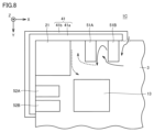
- FIG. 8 is a plan view of the vicinity of one external electrode of an electronic component according to Modification 3. Note that in the configuration of electronic component 1C according to Modification 3, the same components as those in electronic component 1 according to the embodiment are given the same reference numerals and detailed descriptions will not be repeated.
- dummy electrodes 51A, 52A are provided on both sides of side electrode 21 when viewed from the stacking direction (Z direction) with insulating portions sandwiched between them. Furthermore, electronic component 1C has dummy electrodes 51B, 52B (second dummy electrodes) provided at a position farther from side electrode 21 than dummy electrodes 51A, 52A. External electrode 41 is provided from side electrode 21 to the position where dummy electrodes 51B, 52B are provided, and is connected to dummy electrodes 51A, 51B, 52A, 52B on the side of insulator 3.
- dummy electrode 51B in addition to dummy electrode 51A, moisture that penetrates through the gap cannot reach side electrode 21 without bypassing dummy electrode 51A as well as dummy electrode 51B, and the occurrence of defects such as migration occurring between side electrode 21 and internal electrode 13 can be further suppressed.
- dummy electrodes 51B and 52B in addition to dummy electrodes 51A and 52A, the path from the end of the external electrode 41 to the side electrode 21 can be extended, and the path through which moisture can penetrate into the inside of the insulator 3 can be lengthened.
- electronic component 1C may further include multiple dummy electrodes located farther from side electrode 21 than dummy electrodes 51B, 5Bb. While the configuration near external electrode 41 has been described in FIG. 8, electronic component 1C employs a similar configuration near the other external electrodes 42-44.
- dummy electrodes 51-54 of electronic component 1C include dummy electrodes (first dummy electrodes) close to side electrodes 21-24 when viewed from the stacking direction, and dummy electrodes (second dummy electrodes) far from side electrodes 21-24, thereby further reducing the occurrence of problems such as migration between side electrodes and internal electrodes.
- An electronic component formed by laminating a plurality of insulating substrates, each of which includes a side electrode and an internal electrode; an external electrode electrically connected to the side electrode and provided on a side surface of the insulator; the insulating substrates further include dummy electrodes disposed on both sides of the side electrode with an insulating portion interposed therebetween when viewed from the stacking direction; The external electrode is connected to the dummy electrode on the side of the insulator.
- the insulator has a first main surface and a second main surface opposed to each other in the stacking direction; There is no electrical connection by via conductors between the first side electrode closest to the first main surface and the adjacent second side electrode at a position closer to the second main surface than the first side electrode, and between the third side electrode closest to the second main surface and the adjacent fourth side electrode at a position closer to the first main surface than the third side electrode.
- the electronic component according to any one of (1) to (5) The dummy electrodes, as viewed from the lamination direction, have a rectangular shape in which the sides not in contact with the external electrodes are longer than the sides in contact with the external electrodes.
- the dummy electrodes include a first dummy electrode close to the side electrode when viewed from the stacking direction, and a second dummy electrode far from the side electrode.
- the external electrodes include a first external electrode layer provided on a side surface of the insulator and a second external electrode layer covering the first external electrode layer, and the first external electrode layer is in contact with the side surface electrode and the dummy electrode.
- the electronic component according to (8) is The first outer electrode layer is nickel and the second outer electrode layer is gold.
- the side electrodes are provided at the four corners of the insulator when viewed from the stacking direction, and each has a rectangular shape.
- the internal electrodes include at least an electrode that constitutes a part of the coil and an electrode that constitutes a part of the capacitor, and form a filter circuit within the insulator.
- 1, 1A-1C electronic components
- 3 insulator
- 3a-3l insulating substrate
- 11-14 internal electrodes
- 21-24 side electrodes
- 31-36 via conductors
- 41-51 external electrodes
- 51-58 dummy electrodes.
Landscapes
- Engineering & Computer Science (AREA)
- Power Engineering (AREA)
- Manufacturing & Machinery (AREA)
- Microelectronics & Electronic Packaging (AREA)
- Coils Or Transformers For Communication (AREA)
- Fixed Capacitors And Capacitor Manufacturing Machines (AREA)
Priority Applications (2)
| Application Number | Priority Date | Filing Date | Title |
|---|---|---|---|
| JP2025525949A JPWO2024252736A1 (enExample) | 2023-06-06 | 2024-02-20 | |
| CN202480030697.9A CN121153093A (zh) | 2023-06-06 | 2024-02-20 | 电子部件 |
Applications Claiming Priority (2)
| Application Number | Priority Date | Filing Date | Title |
|---|---|---|---|
| JP2023093242 | 2023-06-06 | ||
| JP2023-093242 | 2023-06-06 |
Publications (1)
| Publication Number | Publication Date |
|---|---|
| WO2024252736A1 true WO2024252736A1 (ja) | 2024-12-12 |
Family
ID=93795828
Family Applications (1)
| Application Number | Title | Priority Date | Filing Date |
|---|---|---|---|
| PCT/JP2024/005976 Pending WO2024252736A1 (ja) | 2023-06-06 | 2024-02-20 | 電子部品 |
Country Status (3)
| Country | Link |
|---|---|
| JP (1) | JPWO2024252736A1 (enExample) |
| CN (1) | CN121153093A (enExample) |
| WO (1) | WO2024252736A1 (enExample) |
Citations (7)
| Publication number | Priority date | Publication date | Assignee | Title |
|---|---|---|---|---|
| JPH10154632A (ja) * | 1996-11-22 | 1998-06-09 | Murata Mfg Co Ltd | 3端子コンデンサ |
| JP2012094820A (ja) * | 2010-09-28 | 2012-05-17 | Murata Mfg Co Ltd | 積層セラミック電子部品 |
| JP2012119681A (ja) * | 2010-11-29 | 2012-06-21 | Samsung Electro-Mechanics Co Ltd | 積層セラミックキャパシタ |
| JP2018056543A (ja) * | 2016-09-29 | 2018-04-05 | サムソン エレクトロ−メカニックス カンパニーリミテッド. | 積層型キャパシタ及びその製造方法 |
| JP2018198326A (ja) * | 2018-08-21 | 2018-12-13 | 太陽誘電株式会社 | 積層コンデンサ |
| WO2021215104A1 (ja) * | 2020-04-20 | 2021-10-28 | 株式会社村田製作所 | 電子部品 |
| JP2023062846A (ja) * | 2021-10-22 | 2023-05-09 | Tdk株式会社 | コイル部品及びその製造方法 |
-
2024
- 2024-02-20 WO PCT/JP2024/005976 patent/WO2024252736A1/ja active Pending
- 2024-02-20 JP JP2025525949A patent/JPWO2024252736A1/ja active Pending
- 2024-02-20 CN CN202480030697.9A patent/CN121153093A/zh active Pending
Patent Citations (7)
| Publication number | Priority date | Publication date | Assignee | Title |
|---|---|---|---|---|
| JPH10154632A (ja) * | 1996-11-22 | 1998-06-09 | Murata Mfg Co Ltd | 3端子コンデンサ |
| JP2012094820A (ja) * | 2010-09-28 | 2012-05-17 | Murata Mfg Co Ltd | 積層セラミック電子部品 |
| JP2012119681A (ja) * | 2010-11-29 | 2012-06-21 | Samsung Electro-Mechanics Co Ltd | 積層セラミックキャパシタ |
| JP2018056543A (ja) * | 2016-09-29 | 2018-04-05 | サムソン エレクトロ−メカニックス カンパニーリミテッド. | 積層型キャパシタ及びその製造方法 |
| JP2018198326A (ja) * | 2018-08-21 | 2018-12-13 | 太陽誘電株式会社 | 積層コンデンサ |
| WO2021215104A1 (ja) * | 2020-04-20 | 2021-10-28 | 株式会社村田製作所 | 電子部品 |
| JP2023062846A (ja) * | 2021-10-22 | 2023-05-09 | Tdk株式会社 | コイル部品及びその製造方法 |
Also Published As
| Publication number | Publication date |
|---|---|
| CN121153093A (zh) | 2025-12-16 |
| JPWO2024252736A1 (enExample) | 2024-12-12 |
Similar Documents
| Publication | Publication Date | Title |
|---|---|---|
| CN110036469B (zh) | 高频模块 | |
| CN108109807B (zh) | 电子部件 | |
| US8050045B2 (en) | Electronic component and method of manufacturing the same | |
| JP5333680B2 (ja) | 部品内蔵基板およびその製造方法 | |
| JP7155499B2 (ja) | 積層型電子部品およびその製造方法 | |
| JP6107080B2 (ja) | 積層コンデンサ | |
| KR100970838B1 (ko) | 적층 세라믹 커패시터 | |
| KR100770556B1 (ko) | 적층형 콘덴서 | |
| KR20220116559A (ko) | 박막 캐패시터 및 그 제조 방법 및 박막 캐패시터를 구비하는 전자 회로 기판 | |
| KR20140081360A (ko) | 적층 세라믹 커패시터, 그 제조방법 및 적층 세라믹 커패시터가 실장된 회로기판 | |
| US10827613B2 (en) | Multilayer circuit board, multilayer electronic component, and module | |
| JPWO2013058144A1 (ja) | 複合電子部品 | |
| JP6064860B2 (ja) | 複合電子部品及び複合電子部品の製造方法 | |
| JP6740874B2 (ja) | 電子部品 | |
| JP2021002591A (ja) | 積層コイル部品 | |
| JP5958454B2 (ja) | 部品内蔵モジュール | |
| JP6136507B2 (ja) | 積層コンデンサアレイ | |
| JP6142650B2 (ja) | 積層貫通コンデンサ | |
| CN1776845B (zh) | 层积型电容器 | |
| WO2024252736A1 (ja) | 電子部品 | |
| JP4752280B2 (ja) | チップ型電子部品およびその製造方法 | |
| CN114093592A (zh) | 表面安装型无源部件 | |
| JP4837275B2 (ja) | 積層型コンデンサの実装構造 | |
| JP4975668B2 (ja) | 積層型コンデンサ及びその実装構造 | |
| JP4501524B2 (ja) | セラミック多層基板およびその製造方法 |
Legal Events
| Date | Code | Title | Description |
|---|---|---|---|
| 121 | Ep: the epo has been informed by wipo that ep was designated in this application |
Ref document number: 24818975 Country of ref document: EP Kind code of ref document: A1 |
|
| ENP | Entry into the national phase |
Ref document number: 2025525949 Country of ref document: JP Kind code of ref document: A |
|
| WWE | Wipo information: entry into national phase |
Ref document number: 2025525949 Country of ref document: JP |
|
| WWE | Wipo information: entry into national phase |
Ref document number: CN2024800306979 Country of ref document: CN |