WO2024252624A1 - 電子装置 - Google Patents
電子装置 Download PDFInfo
- Publication number
- WO2024252624A1 WO2024252624A1 PCT/JP2023/021377 JP2023021377W WO2024252624A1 WO 2024252624 A1 WO2024252624 A1 WO 2024252624A1 JP 2023021377 W JP2023021377 W JP 2023021377W WO 2024252624 A1 WO2024252624 A1 WO 2024252624A1
- Authority
- WO
- WIPO (PCT)
- Prior art keywords
- case body
- pair
- electronic device
- cover
- opening
- Prior art date
- Legal status (The legal status is an assumption and is not a legal conclusion. Google has not performed a legal analysis and makes no representation as to the accuracy of the status listed.)
- Ceased
Links
Images




Classifications
-
- H—ELECTRICITY
- H05—ELECTRIC TECHNIQUES NOT OTHERWISE PROVIDED FOR
- H05K—PRINTED CIRCUITS; CASINGS OR CONSTRUCTIONAL DETAILS OF ELECTRIC APPARATUS; MANUFACTURE OF ASSEMBLAGES OF ELECTRICAL COMPONENTS
- H05K5/00—Casings, cabinets or drawers for electric apparatus
- H05K5/0026—Casings, cabinets or drawers for electric apparatus provided with connectors and printed circuit boards [PCB], e.g. automotive electronic control units
- H05K5/0039—Casings, cabinets or drawers for electric apparatus provided with connectors and printed circuit boards [PCB], e.g. automotive electronic control units having a tubular housing wherein the PCB is inserted longitudinally
Definitions
- the present invention relates to an electronic device, and more specifically to an electronic device that houses a circuit board within a housing.
- Vehicles such as automobiles are equipped with electronic devices that house circuit boards inside a housing.
- Some electronic device housings are made up of, for example, a resin case body that houses the circuit board and a cover that covers the opening of the case body.
- the resin case body is manufactured by resin molding using a mold. During this process, factors such as residual stress can cause warping at the opening of the case body, resulting in uneven heights and widths for the opening.
- Patent Document 1 As a countermeasure to such problems, for example, the technology described in Patent Document 1 has been proposed.
- the case side locking part provided on the case engages with the cover side locking part provided on the cover side, thereby holding the cover in a fixed state to the case.
- a snap-fit structure is adopted as a method for fixing the cover to the resin case.
- the outer claw part of the cover which faces closely to the outer surface of the case, presses the case from the outside to the inside of the case opening, thereby correcting bulging of the case opening (dimensional variation that causes unevenness in the height and width of the opening).
- the present invention was made to solve the above problems, and its purpose is to provide an electronic device that can suppress deformation of the case opening that occurs during resin molding using a mold and avoids an increase in the size of the housing.
- an electronic device includes a circuit board constituting an electronic circuit, and a housing that houses the circuit board, the housing having a storage space that covers both sides of the circuit board and stores the circuit board therein, a resin case body having a rectangular opening for inserting the circuit board into the storage space, and a cover that closes the opening of the case body, the case body being formed by four walls: a pair of first side wall portions located opposite both sides of the circuit board, and a pair of second side wall portions connected to one side end and the other side end of the pair of first side wall portions.
- the case body includes a peripheral wall portion having a rectangular cross section that forms the opening, the peripheral wall portion of the case body has a pair of first fitting portions that are provided in the region of the pair of first side wall portions of the annular end face on the opening side and extend along the extending direction of the annular end face, the cover has a pair of second fitting portions that are respectively fitted by press fitting into the pair of first fitting portions of the case body, and the connection portion between the first side wall portion and the second side wall portion of the peripheral wall portion of the case body has a recessed portion on the inner wall surface side that is thinner than the first side wall portion and the second side wall portion.
- a pair of first fitting parts provided on the case body and a pair of second fitting parts provided on the cover form a press-fit fitting structure, so that the cover can be fixed to the case body without providing a snap-fit structure, and the pair of first side walls at the opening of the case body can be made thick to improve rigidity while avoiding an increase in the external dimensions of the housing.
- the recessed part at the corner (the connection part between the first side wall part and the second side wall part) of the peripheral wall part of the case body reduces the difference in contact area between the inner wall surface and the outer wall surface at the corner of the peripheral wall part with the molding die, so that the residual stress generated at the corner is reduced and deformation of the opening of the case body can be suppressed. Therefore, deformation of the opening of the case body that occurs during resin molding using a die can be suppressed and an increase in the size of the housing can be avoided.
- FIG. 1 is a schematic perspective view showing an external appearance of an electronic device according to a first embodiment of the present invention
- 2 is a cross-sectional view of the electronic device according to the first embodiment, taken along the line II-II of FIG. 1.
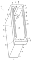
- 2 is a perspective view of a case body of the electronic device according to the first embodiment shown in FIG. 1, as viewed from an opening side.
- 4 is a front view showing the case body of the electronic device according to the first embodiment shown in FIG. 3 from the opening side.
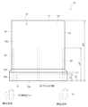
- FIG. 4 is a plan view of a case body of the electronic device according to the first embodiment shown in FIG. 3 .
- FIG. 2 is a perspective view showing a cover of the electronic device according to the first embodiment shown in FIG. 1 .
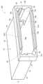
- FIG. 11 is a perspective view of a case body in an electronic device according to a second embodiment of the present invention, as viewed from the opening side.
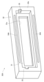
- FIG. 11 is a perspective view showing a cover of an electronic device according to a second embodiment.
- Fig. 1 is a schematic perspective view showing the external appearance of the electronic device according to the first embodiment.
- Fig. 2 is a cross-sectional view of the electronic device according to the first embodiment as seen from the direction of the arrows II-II in Fig. 1.
- the electronic device 1 includes a circuit board 2 (Fig. 2 only) that configures an electronic circuit, and a housing 3 that houses the circuit board 2.
- the electronic device 1 is mounted, for example, on a vehicle (not shown).
- the housing 3 is composed of a cylindrical case body 10 with a bottom, which has an accommodation space 10a for accommodating the circuit board 2 and a rectangular opening 10b on one side for inserting the circuit board 2 into the accommodation space 10a, and a cover 30 attached to the case body 10 so as to cover the opening 10b of the case body 10.
- the case body 10 and the cover 30 are molded resin products. The detailed structure of the case body 10 and the cover 30 of the housing 3 and the method of molding them will be described later.
- the circuit board 2 has a wiring board 5 on which wiring is formed, electronic components (not shown) mounted on the wiring board 5, and a connector 6 mounted on the wiring board 5.
- the wiring board 5 is formed, for example, in a rectangular shape, and has a first surface 5a which is a mounting surface on which the connector 6 is mounted, and a second surface 5b which is the back surface of the first surface 5a.
- the circuit board 2 may be a single-sided mounting in which electronic components are mounted on only one of the first surface 5a and the second surface 5b of the wiring board 5, or a double-sided mounting in which electronic components are mounted on both the first surface 5a and the second surface 5b.
- the connector 6 enables electrical connection with an external electronic device, and is arranged so that a part of it is exposed to the outside of the housing 3 through a connector opening 31a described later in the cover 30 of the housing 3.
- Fig. 3 is a perspective view of the case body of the electronic device according to the first embodiment shown in Fig. 1, as viewed from the opening side.
- Fig. 4 is a front view (as viewed from the opening side) of the case body of the electronic device according to the first embodiment shown in Fig. 3.
- Fig. 5 is a plan view of the case body of the electronic device according to the first embodiment shown in Fig. 3.
- Fig. 6 is a perspective view showing the cover of the electronic device according to the first embodiment shown in Fig. 1.
- the case body 10 of the housing 3 is configured to accommodate the circuit board 2 in the accommodation space 10a so as to cover both the first surface 5a and the second surface 5b of the wiring board 5 and to surround the outer periphery of the wiring board 5 except for the side where the connector 6 is located.
- the case body 10 is formed in a flat, approximately rectangular parallelepiped shape and is composed of a rectangular bottom wall 11 located on the opposite side to the opening 10b of the case body 10, and a square cylindrical peripheral wall 12 rising from the outer periphery of the bottom wall 11.
- the peripheral wall 12 has an opening 10b at its tip end located opposite the bottom wall 11, and has a rectangular annular end face 12a on the opening 10b side.
- the peripheral wall 12 is made up of four walls: a pair of first side wall portions 14 located opposite both the first surface 5a and the second surface 5b of the circuit board 2, and a pair of second side wall portions 15 connected to one end and the other end of the pair of first side wall portions 14, and is formed so that its cross section is rectangular.
- the inner wall surface 15a of the pair of second side wall portions 15 of the peripheral wall 12 is provided with a pair of guide grooves 18 extending from the annular end surface 12a on the opening 10b side of the case body 10 to the bottom wall 11, as shown in Figs. 3 and 4.
- the pair of guide grooves 18 function as guides when the circuit board 2 is inserted into the storage space 10a of the case body 10, and also have the function of holding the lateral ends of the circuit board 2.
- the inner wall surface 11a of the bottom wall 11 is provided with a holding groove 19 extending between the pair of second side wall portions 15, as shown in Fig. 2.
- the holding groove 19 has the function of holding the other side end of the circuit board 2 (the left end in Fig. 2).
- the annular end surface 12a of the peripheral wall 12 on the opening 10b side is the portion against which the frame portion 32 of the cover 30, described later, butts and abuts, as shown in FIG. 2.
- the annular end surface 12a of the peripheral wall 12 is provided with a fitting structure for fixing the cover 30.
- a pair of first fitting portions 21 are provided in the region of the pair of first side wall portions 14 of the annular end surface 12a of the peripheral wall 12.
- the pair of first fitting portions 21 of the peripheral wall 12 are configured as grooves extending along the extending direction of the annular end surface 12a (left-right direction in FIG. 4), as shown in FIG. 4, for example.
- the depth D1 (see FIG. 5) of the grooves as the first fitting portions 21 is set so that the cover 30 is reliably fixed to the case body 10 when the second fitting portion (projection portion) 34 of the cover 30, described later, is fitted by press-fitting.
- the peripheral wall 12 is configured such that the opening side peripheral wall portion 12b, which is the portion located on the opening 10b side including the annular end face 12a, is thicker than the bottom side peripheral wall portion 12c, which is the portion located on the bottom wall 11 side, by forming a groove as the first fitting portion 21. This improves the rigidity of the opening side peripheral wall portion 12b.
- the length L2 of the thick part 12b of the peripheral wall 12 is set to be greater than the depth D1 of the groove as the first fitting portion 21.
- the thick part 12b of the peripheral wall 12 is formed to bulge outwardly and become thicker than the bottom side peripheral wall portion 12c.
- the bottom side peripheral wall portion 12c is configured to have a thickness that ensures the rigidity required when the groove is not formed.
- the peripheral wall 12 has a connecting peripheral wall portion 12d as a connecting portion that connects the bottom side peripheral wall portion 12c, which is thinner than the thick part 12b, to the opening side peripheral wall portion 12b as a thick part.
- the connecting peripheral wall portion 12d is formed in a tapered shape with an outer peripheral surface that widens so that the thickness increases as it approaches the opening side peripheral wall portion 12b as a thick portion.
- the connecting peripheral wall portion 12d connects the opening side peripheral wall portion 12b and the bottom side peripheral wall portion 12c without creating a step.
- the inner wall surface of the peripheral wall 12 (the inner wall surfaces of the opening side peripheral wall portion 12b, the bottom side peripheral wall portion 12c, and the connecting peripheral wall portion 12d) is configured to be aligned with the outer wall surface of the peripheral wall 12, unlike the outer wall surface of the peripheral wall 12.
- the inner wall surface at each corner which is the connection portion between the first side wall portion 14 and the second side wall portion, is formed as a concave wall surface that is a recessed portion 22 relative to the inner wall surface 14a of the first side wall portion 14 and the inner wall surface 15a of the second side wall portion 15, so that the thickness is smaller than the thickness t1 of the first side wall portion 14 and the thickness t2 of the second side wall portion 15, and closer to the outer wall surface 14b of the first side wall portion 14 and the outer wall surface 15b of the second side wall portion 15 than the inner wall surface 14a of the first side wall portion 14 and the inner wall surface 15a of the second side wall portion 15.
- the recessed portion 22 on the inner wall surface of each corner is formed to include an arc-shaped concave surface.
- the arc-shaped concave surface can avoid stress concentration.
- the recessed portion 22 can also be formed as a concave wall surface using a polygonal surface.
- the recessed portion 22 on the inner wall surface of each corner extends from the position of the annular end surface 12a to a position that is equal to or longer than half the depth length D3, L4, of the depth length D3 from one end (annular end surface 12a) on the opening 10b side of the case body 10 to the other end (outer wall surface of the bottom wall 11).
- the case body 10 has a weld area W, which will be described in detail later, where the tips of the resin that flows when the resin is molded using a mold join together. As shown in FIG. 5, there is a concern that the weld area W will be formed from the annular end surface 12a to a length that is half the depth length D3 of the case body 10.
- the weld area W is a portion that tends to have a reduced strength, and it is necessary to suppress deformation of the weld area W. Therefore, the recessed portion 22 is designed to extend to the area where the occurrence of weld areas W is a concern.
- the cover 30 of the housing 3, as shown in Figures 1 and 2, is composed of a rectangular cover body 31 for closing the opening 10b of the case body 10, and a rectangular frame portion 32 provided on the outer periphery of the cover body 31.
- the cover body 31 is provided with a connector opening 31a for exposing a portion of the connector 6 to the outside of the housing 3.
- the frame portion 32 is a portion that fixes the cover 30 to the case body 10, and has an abutment surface 32a that abuts against the annular end portion 12a of the case body 10.
- a pair of second fitting portions 34 that fit into the pair of first fitting portions 21 of the case body 10 by press-fitting are provided on the abutment surface 32a of the frame portion 32 that abuts against the area of the pair of first side wall portions 14 of the annular end surface 12a of the case body 10.
- the second fitting portions 34 of the cover 30 are configured as ridge portions that are pressed into the grooves 21 of the case body 10, for example, as shown in FIGS. 2 and 6.
- the ridge portions as the second fitting portions 34 of the cover 30 extend along the extension direction of the frame portion 32.
- the dimensional relationship between the protrusion portion as the second fitting portion 34 of the cover 30 and the groove as the first fitting portion 21 of the case body 10 is set, for example, within the range of light press-fit.
- the range of light press-fit in JIS B0401-2 includes a combination of H6 on the groove 21 side and js5, jk5, m5, n5, and n6 on the protrusion portion 34 side, or a combination of H7 on the groove 21 side and k6, m6, n6, and p6 on the protrusion portion 34 side.
- the frame 32 has a pair of notches 35 that connect to the guide groove 18 of the case body 10 in the portion of the abutment surface 32a that abuts against the area of the pair of second side wall portions 15 of the annular end face 12a of the case body 10.
- the pair of notches 35 are configured to hold the corner portion of one side edge of the circuit board 2 where the connector 6 is located.
- FIG. 7 is an explanatory diagram showing the resin molding method for the case body of the electronic device according to the first embodiment.
- the case body 10 of the electronic device 1 shown in FIG. 3 is resin molded using a mold that combines a female mold (cavity) 101 as shown in FIG. 7 with a male mold (core) (not shown).
- the molding system 100 for the case body 10 according to this embodiment shown in FIG. 7 is a multi-cavity system that has a number of female molds (cavities) 101 and corresponding male molds (cores).
- a nozzle 102 that injects molten resin is connected to a number of female molds (cavities) 101 via runners 103.
- the molding system 100 capable of multiple molds improves yield and enables low-cost production.
- the cover 30 can also be resin molded using a similar molding system.
- the female mold (cavity) 101 is arranged so that the part corresponding to the bottom wall 11 of the case body 10 faces upward and the part corresponding to the opening 10b of the peripheral wall 12 faces downward.
- the female mold (cavity) 101 has a gate 101a formed in the part corresponding to the bottom wall 11 of the case body 10.
- the molten resin that flows into the female mold (cavity) 101 through the gate 101a flows from the part corresponding to the bottom wall 11 of the case body 10 toward the part corresponding to the annular end face 12a.
- a weld area W is likely to be formed in the center of the opening side of the pair of first side wall portions 14 in the peripheral wall 12 of the case body 10.
- the weld area W formed in this way will be formed from the annular end face 12a to a length that is half the depth length D3 of the case body 10.
- the mold is opened by moving a male mold (core) (not shown) downward.
- the case body 10 can be released from the male mold (core) by pushing it upward using, for example, a cylindrical push-out pin P as shown in FIG. 5.
- the push-out pin P is arranged in a position such that it pushes out a corner of the annular end face 12a of the peripheral wall 12.
- a plate-shaped square pin P can be used as shown in FIG. 7. In this configuration, it is arranged so as to push out the area of a pair of first side wall portions 14 or second side wall portions 15 on the annular end face 12a of the peripheral wall 12.
- each corner of the opening 10b side of the peripheral wall 12 of the case body 10 has a recessed portion 22 on the inner wall surface side such that it is thinner than the first side wall portion 14 and the second side wall portion 15.
- the difference between the contact area of the outer wall surface with the female mold (cavity) 101 and the contact area of the inner wall surface with the male mold (core) at the corners of the opening 10b side of the peripheral wall 12 is smaller than when the recessed portion 22 is not provided, thereby reducing residual stress that occurs at the corners during resin molding using the mold for the case body 10.
- warping of the opening of the case body 10 can be suppressed.
- a groove, which is the first fitting portion 21, is provided in the region of a pair of first side wall portions 14 of the annular end surface 12a of the case body 10 as a press-fit fitting structure for fixing the cover 30 to the case body 10. Therefore, since the cover 30 can be fixed to the case body 10 without providing a snap-fit structure, a sliding mold required when molding a snap-fit structure is not required, and the molding system 100 for the case body 10 can be simplified.
- the electronic device 1 includes a circuit board 2 constituting an electronic circuit, and a housing 3 that houses the circuit board 2 therein.
- the housing 3 includes a resin case body 10 having an accommodation space 10a that accommodates the circuit board 2 so as to cover both sides 5a, 5b of the circuit board 2, and a rectangular opening 10b for inserting the circuit board 2 into the accommodation space 10a, and a cover 30 that closes the opening 10b of the case body 10.
- the case body 10 includes a peripheral wall portion (the portion of the peripheral wall 12 on the opening 10b side) having a rectangular cross section that forms the opening 10b, with four walls: a pair of first side wall portions 14 located opposite both sides 5a, 5b of the circuit board 2, and a pair of second side wall portions 15 connected to one side end and the other side end of the pair of first side wall portions 14.
- the peripheral wall of the case body 10 has a pair of first fitting portions 21 that are provided in the region of a pair of first side wall portions 14 of the annular end face 12a on the opening 10b side and extend along the extending direction of the annular end face 12a.
- the cover 30 has a pair of second fitting portions 34 that are press-fitted into the pair of first fitting portions 21 of the case body 10.
- the connection portion between the first side wall portion 14 and the second side wall portion 15 of the peripheral wall of the case body 10 has a recessed portion 22 on the inner wall surface side that is thinner than the first side wall portion 14 and the second side wall portion 15.
- a pair of first fitting parts 21 provided on the case body 10 and a pair of second fitting parts 34 provided on the cover 30 form a press-fit fitting structure, so that the cover 30 can be fixed to the case body 10 without providing a snap-fit structure.
- This makes it possible to thicken the pair of first side wall parts 14 at the opening of the case body 10 to improve rigidity while avoiding an increase in the external dimensions of the housing 3.
- the recessed part 22 at the corner (the connection part of the first side wall part 14 and the second side wall part 15) of the peripheral wall part (the part on the opening 10b side of the peripheral wall 12) of the case body 10 reduces the difference in contact area between the inner wall surface and the outer wall surface with the molding die at the corner of the peripheral wall part, thereby reducing residual stress generated at the corner and suppressing deformation of the opening of the case body 10. Therefore, deformation of the opening of the case body 10 that occurs during resin molding using a die can be suppressed, and an increase in the size of the housing 3 can be avoided.
- the occurrence of gaps between the case body 10 and the cover 30, which can be a route for water to enter the case body 10, is suppressed.
- the press-fit mating structure between the case body 10 and the cover 30 within the tolerance range of a light press-fit, it is possible to ensure a sealed structure for the housing 3. Therefore, water resistance can be maintained with just the press-fit structure between the first mating portion 21 of the case body 10 and the second mating portion 34 of the cover 30.
- the recessed portion 22 at the connection portion (corner portion) of the first side wall portion 14 and the second side wall portion 15 of the peripheral wall portion is formed to include an arc-shaped concave curved surface.
- This configuration makes it possible to avoid stress concentration on the inner wall surface of each corner of the peripheral wall.
- the recessed portion 22 extends from the position of the annular end face 12a to a position L4 that is equal to or greater than half the depth length D3 from one end to the other end of the opening 10b side of the case body 10.
- the pair of first fitting portions 21 of the case body 10 are grooves extending along the extension direction of the annular end face 12a, and the pair of second fitting portions 34 of the cover 30 are protrusions that are pressed into the grooves 21 of the case body 10.
- the fitting structure for fixing the case body 10 and the cover 30 is a simplified press-fit structure, which simplifies the mold for resin molding the case body 10 and the cover 30.
- peripheral wall portion (the portion of the peripheral wall 12 on the opening 10b side) of the case body 10 in this embodiment is formed as a thick portion in which the portion (opening side peripheral wall portion 12b) from the annular end face 12a to at least the position of the depth D1 of the groove that is the first fitting portion 21 bulges outward more toward the outer periphery than the other portion of the case body 10 (bottom side peripheral wall portion 12c) and is thicker.
- the portion of the case body 10 on the opening 10b side is made thicker as the thicker portion 12b, improving rigidity, and making it possible to suppress deformation due to loads applied when the case body 10 is demolded and when the cover is attached.
- connecting peripheral wall portion 12d in a tapered shape with an expanding outer circumferential surface, it is possible to connect the opening side peripheral wall portion 12b, which is a thick portion, and the bottom side peripheral wall portion 12c, which is a relatively thin portion, without creating a step. This makes it possible to avoid stress concentration occurring in the connecting peripheral wall portion 12d.
- Figure 8 is a perspective view of a case body in an electronic device according to the second embodiment of the present invention, as viewed from the opening side.
- Figure 9 is a perspective view showing a cover of an electronic device according to the second embodiment.
- the same reference numerals as those in Figures 1 to 7 denote similar parts, and therefore detailed description thereof will be omitted.
- the electronic device according to the second embodiment shown in Figures 8 and 9 differs from the first embodiment in that the press-fit fitting structure between the case body 10A of the housing and the cover 30A is inverted.
- the rest of the configuration and structure of the electronic device according to the second embodiment is similar to the structure of the electronic device 1 according to the first embodiment, and a description thereof will be omitted.
- a pair of grooves are provided as second fitting portions 34A into which the protrusions serving as a pair of first fitting portions 21 of the case body 10 are press-fitted on the abutment surface 32a of the frame portion 32 that abuts against the area of a pair of first side wall portions 14 of the annular end surface 12a of the case body 10.
- the grooves serving as the second fitting portions 34A of the cover 30 extend along the extension direction of the frame portion 32.
- the protrusion 21A on the annular end surface 12a of the case body 10A and the groove 34A on the abutment surface 32a of the cover 30A form a press-fit structure that fixes the cover 30A to the case body 10A. Therefore, the cover 30A can be fixed to the case body 10A without providing a snap-fit structure, eliminating the need for a sliding mold that is required when molding a snap-fit structure, and simplifying the molding system 100 for the case body 10A.
- the recessed part 22 at the corner (the connection part of the first side wall part 14 and the second side wall part 15) of the peripheral wall part (the part on the opening 10b side of the peripheral wall 12) of the case body 10A reduces the difference in contact area between the inner wall surface and the outer wall surface with the molding die at the corner of the peripheral wall part, thereby reducing residual stress generated at the corner and suppressing deformation of the opening of the case body 10A. This makes it possible to suppress deformation of the opening of the case body 10A that occurs during resin molding using a mold, and to avoid an increase in the size of the housing 3.
- the occurrence of gaps between the case body 10A and the cover 30A, which can be a route for water to enter the case body 10A, is suppressed.
- the press-fit mating structure between the case body 10A and the cover 30A within the tolerance range of a light press-fit, it is possible to ensure a sealed structure for the housing 3. Therefore, water resistance can be maintained with just the press-fit structure between the first mating portion 21A of the case body 10A and the second mating portion 34A of the cover 30A.
- the pair of first fitting portions 21A of the case body 10A are ridge portions that protrude from the annular end face 12a toward the cover 30A and extend along the extension direction of the annular end face 12a.
- the pair of second fitting portions 34A of the cover 30A are grooves into which the pair of ridge portions serving as the first fitting portions 21A of the case body 10A are press-fitted.
- the fitting structure for fixing the case body 10A and the cover 30A is a simplified press-fit structure, which simplifies the molds for resin molding the case body 10A and the cover 30A.
- the present invention is not limited to the above-described embodiment, and includes various modified examples.
- the above-described embodiment has been described in detail to easily explain the present invention, and is not necessarily limited to those having all of the configurations described. It is possible to replace a part of the configuration of one embodiment with the configuration of another embodiment, and it is also possible to add the configuration of another embodiment to the configuration of one embodiment. It is also possible to add, delete, or replace a part of the configuration of each embodiment with another configuration.
- the electronic device can also be configured so that the connector is not mounted on the circuit board, for example, when transmitting information to an external electronic device via communication.
- the recessed portion 22 in the corner (the connection portion between the first side wall portion 14 and the second side wall portion 15) of the case body 10, 10A is formed from the annular end face 12a to a position of length L4 that is half or more of the depth length D3 of the case body 10, 10A.
- the recessed portion 22 it is also possible for the recessed portion 22 to extend only over the range of the opening side peripheral wall portion 12b as the thick portion.
- this configuration may result in a reduced effect of suppressing warping (deformation) of the opening of the case body 10, 10A compared to the above-described embodiment.
- peripheral wall 12 of the case body 10, 10A has a rectangular cross section from the annular end face 12a to the bottom wall 11.
- the peripheral wall 12 has a rectangular cross section up to the position where the corner recess 22 extends, the cross section beyond that point can be configured in a non-rectangular shape.
- 1...electronic device 2...circuit board, 5a...first surface, 5b...second surface, 3...housing, 10, 10A...case body, 10a...accommodation space, 10b...opening, 12...peripheral wall, 12a...annular end face, 12b...opening side peripheral wall (thick part), 12c...bottom side peripheral wall (thin part), 12d...connecting peripheral wall (connecting part), 14...first side wall, 15...second side wall, 21...first fitting part (groove), 21A...first fitting part (projection), 22...recess, 30, 30A...cover, 34...second fitting part (projection), 34A...second fitting part (groove)
Landscapes
- Engineering & Computer Science (AREA)
- Microelectronics & Electronic Packaging (AREA)
- Casings For Electric Apparatus (AREA)
Abstract
Description
上記した以外の課題、構成及び効果は、以下の実施形態の説明により明らかにされる。
[第1の実施形態]
まず、第1の実施形態に係る電子装置の構成について図1及び図2を用いて説明する。図1は第1の実施形態に係る電子装置の外観を示す概略斜視図である。図2は第1の実施形態に係る電子装置を図1のII-II矢視から見た断面図である。
次に、本発明の第2の実施形態に係る電子装置について図8及び図9を用いて説明する。図8は本発明の第2の実施形態に係る電子装置におけるケース本体を開口部側から見た斜視図である。図9は第2の実施形態に係る電子装置のカバーを示す斜視図である。なお、図8及び図9において、図1~図7に示す符号と同符号のものは、同様な部分であるので、その詳細な説明は省略する。
なお、本発明は上述した実施の形態に限られるものではなく、様々な変形例が含まれる。上記した実施形態は本発明をわかり易く説明するために詳細に説明したものであり、必ずしも説明した全ての構成を備えるものに限定されるものではない。ある実施形態の構成の一部を他の実施の形態の構成に置き換えることが可能であり、また、ある実施形態の構成に他の実施の形態の構成を加えることも可能である。また、各実施形態の構成の一部について、他の構成の追加、削除、置換をすることも可能である。
Claims (7)
- 電子回路を構成する回路基板と、
前記回路基板を内部に収容する筐体とを備え、
前記筐体は、
前記回路基板の両面側を覆うように前記回路基板を収容する収容空間を有すると共に、前記回路基板を前記収容空間内に挿入するための矩形状の開口を有する樹脂製のケース本体と、
前記ケース本体の前記開口を塞ぐカバーとを備え、
前記ケース本体は、前記回路基板の両面に対向する位置にある一対の第1辺壁部と前記一対の第1辺壁部の一方側端部及び他方側端部に接続される一対の第2辺壁部との4つの壁部によって、前記開口を形成する横断面矩形状の周壁部を含み、
前記ケース本体の前記周壁部は、前記開口側の環状端面のうち前記一対の第1辺壁部の領域にそれぞれ設けられ、前記環状端面の延在方向に沿って延在する一対の第1嵌合部を有し、
前記カバーは、前記ケース本体の前記一対の第1嵌合部に対してそれぞれ圧入により嵌合する一対の第2嵌合部を有し、
前記ケース本体の前記周壁部における前記第1辺壁部と前記第2辺壁部との接続部分は、前記第1辺壁部及び前記第2辺壁部よりも薄肉となるような凹み部を内壁面側に有している
ことを特徴とする電子装置。 - 請求項1に記載の電子装置において、
前記周壁部の前記接続部分における前記凹み部は、円弧状の凹曲面を含むように形成されている
ことを特徴とする電子装置。 - 請求項1に記載の電子装置において、
前記周壁部の前記接続部分における前記凹み部は、前記ケース本体の前記開口側の一方端から他方端までの奥行長さのうち、前記環状端面の位置から前記奥行長さの2分の1の長さ以上の位置まで延在している
ことを特徴とする電子装置。 - 請求項1に記載の電子装置において、
前記ケース本体の前記一対の第1嵌合部は、前記環状端面の延在方向に沿って延在する条溝であり、
前記カバーの前記一対の第2嵌合部は、前記ケース本体の前記条溝に圧入する突条部である
ことを特徴とする電子装置。 - 請求項1に記載の電子装置において、
前記ケース本体の前記一対の第1嵌合部は、前記環状端面から前記カバー側に向かって突出すると共に前記環状端面の延在方向に沿って延在する突条部であり、
前記カバーの前記一対の第2嵌合部は、前記ケース本体の前記突条部が圧入される条溝である
ことを特徴とする電子装置。 - 請求項4に記載の電子装置において、
前記ケース本体の前記周壁部は、前記環状端面から少なくとも前記条溝の深さの位置までの部分が前記ケース本体のそれ以外の部分よりも外周側に膨出して厚みが厚くなる厚肉部として形成されている
ことを特徴とする電子装置。 - 請求項6に記載の電子装置において、
前記ケース本体は、前記厚肉部よりも厚みが小さい薄肉部と前記厚肉部とを接続する接続部を有し、
前記接続部は、前記厚肉部に近づくにつれて厚みが厚くなるように外周面が拡がるテーパ状に形成されている
ことを特徴とする電子装置。
Priority Applications (4)
| Application Number | Priority Date | Filing Date | Title |
|---|---|---|---|
| CN202380095063.7A CN120826988A (zh) | 2023-06-08 | 2023-06-08 | 电子装置 |
| PCT/JP2023/021377 WO2024252624A1 (ja) | 2023-06-08 | 2023-06-08 | 電子装置 |
| DE112023005413.4T DE112023005413T5 (de) | 2023-06-08 | 2023-06-08 | Elektronische vorrichtung |
| JP2025525869A JPWO2024252624A1 (ja) | 2023-06-08 | 2023-06-08 |
Applications Claiming Priority (1)
| Application Number | Priority Date | Filing Date | Title |
|---|---|---|---|
| PCT/JP2023/021377 WO2024252624A1 (ja) | 2023-06-08 | 2023-06-08 | 電子装置 |
Publications (1)
| Publication Number | Publication Date |
|---|---|
| WO2024252624A1 true WO2024252624A1 (ja) | 2024-12-12 |
Family
ID=93795659
Family Applications (1)
| Application Number | Title | Priority Date | Filing Date |
|---|---|---|---|
| PCT/JP2023/021377 Ceased WO2024252624A1 (ja) | 2023-06-08 | 2023-06-08 | 電子装置 |
Country Status (4)
| Country | Link |
|---|---|
| JP (1) | JPWO2024252624A1 (ja) |
| CN (1) | CN120826988A (ja) |
| DE (1) | DE112023005413T5 (ja) |
| WO (1) | WO2024252624A1 (ja) |
Citations (1)
| Publication number | Priority date | Publication date | Assignee | Title |
|---|---|---|---|---|
| JPH0557537U (ja) * | 1992-01-13 | 1993-07-30 | エスエムシー株式会社 | 多連切換弁 |
Family Cites Families (3)
| Publication number | Priority date | Publication date | Assignee | Title |
|---|---|---|---|---|
| JPH0727238U (ja) * | 1993-10-25 | 1995-05-19 | 矢崎総業株式会社 | 電気接続箱 |
| JP7221811B2 (ja) * | 2019-06-14 | 2023-02-14 | 矢崎総業株式会社 | 分岐ユニット |
| JP7337681B2 (ja) * | 2019-12-10 | 2023-09-04 | 新電元工業株式会社 | 電子装置 |
-
2023
- 2023-06-08 WO PCT/JP2023/021377 patent/WO2024252624A1/ja not_active Ceased
- 2023-06-08 CN CN202380095063.7A patent/CN120826988A/zh active Pending
- 2023-06-08 DE DE112023005413.4T patent/DE112023005413T5/de active Pending
- 2023-06-08 JP JP2025525869A patent/JPWO2024252624A1/ja active Pending
Patent Citations (1)
| Publication number | Priority date | Publication date | Assignee | Title |
|---|---|---|---|---|
| JPH0557537U (ja) * | 1992-01-13 | 1993-07-30 | エスエムシー株式会社 | 多連切換弁 |
Also Published As
| Publication number | Publication date |
|---|---|
| JPWO2024252624A1 (ja) | 2024-12-12 |
| CN120826988A (zh) | 2025-10-21 |
| DE112023005413T5 (de) | 2025-10-16 |
Similar Documents
| Publication | Publication Date | Title |
|---|---|---|
| JP2513946Y2 (ja) | コネクタ | |
| US11626676B2 (en) | Connector and method for manufacturing same | |
| JPH10193363A (ja) | コネクタの製造方法及びインサート成形コネクタ | |
| JP4356548B2 (ja) | 基板用コネクタ | |
| US11411343B2 (en) | Circuit board device and board connector | |
| US20190297737A1 (en) | Electronic component module, electric connection box, and wire harness | |
| JP4742877B2 (ja) | 樹脂成形品の成形構造 | |
| EP3537547A1 (en) | Electric plug with elastic press-on elements | |
| JP2016157529A (ja) | コネクタ組立体 | |
| CN106058543A (zh) | 连接器 | |
| US20120121969A1 (en) | Battery pack case and method for manufacturing the same, and battery pack and method for manufacturing the same | |
| JP2008293950A (ja) | コネクタ及びコネクタの製造方法 | |
| CN112335134B (zh) | 电路基板装置 | |
| US5938481A (en) | Connector and method for manufacturing the same | |
| JP5237022B2 (ja) | 雌型コネクタ、モータケース、モータユニットおよびモータケースの製造方法 | |
| JP2014194854A (ja) | ケース一体型コネクタ及びその製造方法 | |
| CN113574743B (zh) | 连接器 | |
| CN120826988A (zh) | 电子装置 | |
| US7776247B2 (en) | Method of manufacturing electronic device having resin-molded case and molding tool for forming resin-molded case | |
| JPH11289178A (ja) | 電子制御装置の筐体構造 | |
| JP7019271B2 (ja) | 電気接続箱 | |
| JPH10190256A (ja) | 配線基板の固定構造 | |
| JP7818960B2 (ja) | 通信コネクタ | |
| US11502457B2 (en) | Substrate protection structure during inner housing assembling | |
| JP2020205678A (ja) | 分岐ユニット |
Legal Events
| Date | Code | Title | Description |
|---|---|---|---|
| 121 | Ep: the epo has been informed by wipo that ep was designated in this application |
Ref document number: 23940722 Country of ref document: EP Kind code of ref document: A1 |
|
| WWE | Wipo information: entry into national phase |
Ref document number: 112023005413 Country of ref document: DE |
|
| WWE | Wipo information: entry into national phase |
Ref document number: 202380095063.7 Country of ref document: CN |
|
| ENP | Entry into the national phase |
Ref document number: 2025525869 Country of ref document: JP Kind code of ref document: A |
|
| WWE | Wipo information: entry into national phase |
Ref document number: 2025525869 Country of ref document: JP |
|
| WWE | Wipo information: entry into national phase |
Ref document number: 202517082959 Country of ref document: IN |
|
| WWP | Wipo information: published in national office |
Ref document number: 202517082959 Country of ref document: IN |
|
| WWP | Wipo information: published in national office |
Ref document number: 112023005413 Country of ref document: DE |
|
| WWP | Wipo information: published in national office |
Ref document number: 202380095063.7 Country of ref document: CN |
|
| 122 | Ep: pct application non-entry in european phase |
Ref document number: 23940722 Country of ref document: EP Kind code of ref document: A1 |