WO2024252620A1 - 撮像モジュール、内視鏡、および、撮像モジュールの製造方法 - Google Patents
撮像モジュール、内視鏡、および、撮像モジュールの製造方法 Download PDFInfo
- Publication number
- WO2024252620A1 WO2024252620A1 PCT/JP2023/021361 JP2023021361W WO2024252620A1 WO 2024252620 A1 WO2024252620 A1 WO 2024252620A1 JP 2023021361 W JP2023021361 W JP 2023021361W WO 2024252620 A1 WO2024252620 A1 WO 2024252620A1
- Authority
- WO
- WIPO (PCT)
- Prior art keywords
- main surface
- imaging module
- lands
- wiring
- lead
- Prior art date
- Legal status (The legal status is an assumption and is not a legal conclusion. Google has not performed a legal analysis and makes no representation as to the accuracy of the status listed.)
- Ceased
Links
Images






Classifications
-
- A—HUMAN NECESSITIES
- A61—MEDICAL OR VETERINARY SCIENCE; HYGIENE
- A61B—DIAGNOSIS; SURGERY; IDENTIFICATION
- A61B1/00—Instruments for performing medical examinations of the interior of cavities or tubes of the body by visual or photographical inspection, e.g. endoscopes; Illuminating arrangements therefor
- A61B1/04—Instruments for performing medical examinations of the interior of cavities or tubes of the body by visual or photographical inspection, e.g. endoscopes; Illuminating arrangements therefor combined with photographic or television appliances
- A61B1/05—Instruments for performing medical examinations of the interior of cavities or tubes of the body by visual or photographical inspection, e.g. endoscopes; Illuminating arrangements therefor combined with photographic or television appliances characterised by the image sensor, e.g. camera, being in the distal end portion
- A61B1/051—Details of CCD assembly
-
- A—HUMAN NECESSITIES
- A61—MEDICAL OR VETERINARY SCIENCE; HYGIENE
- A61B—DIAGNOSIS; SURGERY; IDENTIFICATION
- A61B1/00—Instruments for performing medical examinations of the interior of cavities or tubes of the body by visual or photographical inspection, e.g. endoscopes; Illuminating arrangements therefor
- A61B1/00064—Constructional details of the endoscope body
- A61B1/0011—Manufacturing of endoscope parts
Definitions
- the present invention relates to an imaging module having a camera unit disposed therein, an endoscope having an imaging module having a camera unit disposed therein, and a method for manufacturing an imaging module having a camera unit disposed therein.
- MIDs molded interconnect devices
- JP Patent Publication 2017-23234 A discloses an endoscope camera unit that uses an irregular circuit board, which is a three-dimensional circuit device.
- the camera unit includes an image sensor, a flat wiring board (planar wiring board) on which electronic components are mounted, and an irregular circuit board (three-dimensional wiring board). Multiple cables are joined to each of the multiple side surfaces of the irregular circuit board.
- WO 2021/181530 discloses an imaging module in which a camera unit is mounted in the cavity of a molded circuit device.
- the external electrode of the camera unit is connected to a signal cable via a through-hole wiring that penetrates the bottom surface of the cavity and reaches the back surface.
- the object of the present invention is to provide a high-performance imaging module with a precisely joined camera unit, an endoscope having a highly-performance imaging module with a precisely joined camera unit, and a method for manufacturing an imaging module with a precisely joined camera unit.
- the imaging module of one aspect of the present invention has a first main surface and a second main surface opposite to the first main surface, and is provided with a plurality of lands and a plurality of lead-out wirings extending from each of the lands on the first main surface, a plurality of through holes penetrating the first main surface and the second main surface, and a plurality of through wiring layers electrically connected to each of the lead-out wirings are provided on the inner surface of each of the plurality of through holes, a plurality of resins disposed in each of the plurality of through holes and sealing the opening on the first main surface side, a plurality of bonding members bonded to each of the plurality of lands, and a camera unit bonded to the plurality of bonding members.
- An endoscope has an insertion section including a tip end on which an imaging module is disposed, and the imaging module has a first main surface and a second main surface opposite the first main surface, and the first main surface is provided with a plurality of lands and a plurality of lead wires extending from each of the lands, a wiring board having a plurality of through holes penetrating the first main surface and the second main surface, and a plurality of through wiring layers electrically connected to each of the lead wires are disposed on the inner surface of each of the plurality of through holes, a plurality of resins disposed in each of the plurality of through holes and sealing the opening on the first main surface side, a plurality of bonding members bonded to each of the plurality of lands, and a camera unit bonded to the plurality of bonding members.
- a method for manufacturing an imaging module includes the steps of: producing a wiring board having a first main surface and a second main surface opposite to the first main surface, a plurality of lands and a plurality of lead-out wirings extending from each of the lands arranged on the first main surface, a plurality of through holes penetrating the first main surface and the second main surface, and a plurality of through wiring layers electrically connected to each of the lead-out wirings arranged on the inner surface of each of the plurality of through holes; sealing the openings of the plurality of through wiring layers on the first main surface side by disposing a plurality of resins in each of the plurality of through holes; and joining each of a plurality of external electrodes of a camera unit to each of the plurality of lands using a joining member.
- a high-performance imaging module with a precisely joined camera unit an endoscope having a high-performance imaging module with a precisely joined camera unit, and a method for manufacturing an imaging module with a precisely joined camera unit.
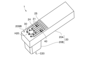
- FIG. 2 is a perspective view of the imaging module according to the first embodiment.
- FIG. 2 is a perspective view of the imaging module according to the first embodiment.
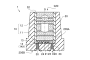
- 3 is a cross-sectional view taken along line III-III in FIG. 1.
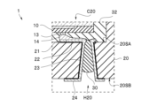
- FIG. 4 is a partially enlarged view of FIG. 3 .
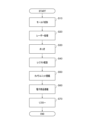
- 4 is a flowchart of a method for manufacturing the image pickup module according to the first embodiment.
- FIG. 2 is a perspective view of a base of a wiring board of the imaging module according to the first embodiment.
- 5A to 5C are partial cross-sectional views for explaining a manufacturing method of the imaging module of the first embodiment.
- 5A to 5C are partial cross-sectional views for explaining a manufacturing method of the imaging module of the first embodiment.
- FIG. 2 is a bottom view of the camera unit of the imaging module according to the first embodiment.
- 4 is a bottom view of a cavity in a wiring board of the imaging module according to the first embodiment.
- FIG. 4 is a bottom view of a cavity in a wiring board of the imaging module according to the first embodiment.
- FIG. 11 is a perspective view of an endoscope according to a second embodiment.
- 13 is a perspective view of a main portion of a tip member of an endoscope according to a second embodiment.
- FIG. 17 is a cross-sectional view taken along line XVII-XVII in FIG. 16.
- First Embodiment 1 to 4 show an imaging module 1 of the present embodiment.
- the imaging module 1 has a wiring board 20 and a camera unit 10.
- the wiring board 20 is a three-dimensional wiring board that is a molded interconnect device (MID).
- Wiring board 20 is a three-dimensional (solid) molded circuit device in which multiple conductor patterns and the like are arranged on an injection-molded three-dimensional substrate. Unlike conventional flat wiring boards, by using wiring board 20, the shape has a function, and furthermore, conductor patterns can be formed on inclined surfaces, vertical surfaces, curved surfaces, through holes, etc.
- the wiring board 20 has an assembly member 20A and a protrusion 20B protruding from the assembly member 20A.
- the protrusion 20B which is surrounded by a picture-frame-shaped wall, forms a cavity C20, which is a bottomed hole in which the camera unit 10 is housed.
- the gap between the camera unit 10 housed in the cavity C20 and the inner wall surface 20SS of the cavity C20 is filled with sealing resin 32.
- the bottom surface of the cavity C20 is referred to as the first main surface 20SA
- the surface opposite the first main surface 20SA is referred to as the second main surface 20SB.
- the camera unit 10 includes an imager 11 and an optical element 12.
- the optical element 12 includes a number of lenses, etc.
- the imager 11 is an imaging element such as a CCD or CMOS that converts the subject image collected by the optical element 12 into an electrical signal.
- the camera unit 10 (imager 11) has multiple external electrodes 13 on the bottom surface 10SB that transmit and receive electrical signals. Solder bumps 14X (see FIG. 12) are provided on each of the external electrodes 13 to form a ball grid array.
- the camera unit 10 is joined to the wiring board 20 by solder 14, which is a joining material formed by melting the solder bumps 14X.
- the wiring board 20 has a plurality of through holes H20 penetrating the first main surface 20SA and the second main surface 20SB.
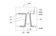
- a through wiring layer 23 is disposed on the inner surface of the through holes H20.
- resin 30 is disposed in the through holes H20.
- a wiring pattern 24 extending from the through wiring layer 23 and a pad 25 provided at an end of the wiring pattern 24 are disposed on the second main surface 20SB.
- a plurality of solder resist patterns 31 are arranged on the wiring pattern 24 on the second main surface 20SB.
- An electronic component for example, a chip capacitor 40, is surface mounted on the two wiring patterns 24 between the two solder resist patterns 31.
- the solder resist patterns 31 are arranged in order to mount electronic components on the two wiring patterns 24 arranged in parallel.
- a signal cable is joined to the pad 25.
- lands 21 On the first main surface 20SA, there are arranged lands 21 and lead-out wiring 22 extending from the lands 21. The ends of the lead-out wiring 22 are connected to the through wiring layer 23.
- the land 21, the lead-out wiring 22, the through wiring layer 23, the wiring pattern 24, and the pad 25 are conductive layers that are formed simultaneously, and the boundaries between them are not clear.
- the external electrodes 13 of the camera unit 10 are joined to the lands 21 of the wiring board 20 by the solder 14 formed by melting the solder bumps 14X.
- the melted solder 14 spreads from the lands 21 to the lead-out wiring 22 when joined.
- the inner diameter of the through hole H20 is greater than twice the thickness of the through wiring layer 23.
- the through hole H20 is not blocked by the through wiring layer 23, and has an opening on the first main surface 20SA. However, this opening is blocked by the resin 30. Therefore, the molten solder 14 does not flow into the through hole.
- the camera unit 10 when the camera unit 10 is joined to the wiring board 20, if the unfixed camera unit 10 melts the solder bumps 14X, there is a risk that the solder 14 will move in the direction that the solder flows out. Furthermore, if the solder 14 flows into the through holes H20, there is a risk that the bond between the external electrodes 13 and the lands 21 will be weakened, or that the camera unit 10 will be joined at an angle.
- the opening of the first main surface 20SA of the through hole H20 is sealed with resin 30, so the camera unit 10 is accurately bonded to the desired position of the wiring board 20. This provides high performance to the imaging module 1.
- Step S10 Molding (molded substrate manufacturing process) MID resin is injected into a mold (not shown) that includes a recess in the shape of wiring board 20, and molded substrate 20X as shown in Fig. 6 is produced by injection molding.
- a precursor such as a non-conductive metal complex that becomes a plating catalyst when irradiated with light is added to the MID resin.
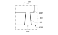
- a through hole H20 is formed from the second main surface 20SB to the first main surface 20SA by irradiating a high-power laser from the second main surface 20SB of the molded substrate 20X.
- the opening of the through hole H20 in the second main surface 20SB is larger than that in the first main surface 20SA.
- the inner dimension of the through hole H20 increases from the first main surface 20SA to the second main surface 20SB.
- An activated catalyst layer 29 is formed on the wall surface of the through hole H20.
- a laser is irradiated in a pattern onto the first main surface 20SA and the second main surface 20SB in order to arrange the lands 21, the lead wiring 22, the wiring pattern 24, and the pads 25.
- a catalyst layer 29 having catalytic activity for electroless plating is formed.
- the outer peripheral end of the lead-out wiring 22 is more than a predetermined distance L from the inner wall surface 20SS of the cavity C20.
- the predetermined distance L is, for example, preferably more than 0.1 mm, and particularly preferably more than 0.2 mm.
- the molded substrate 20X becomes the wiring board 20 having a conductor pattern disposed on the first main surface 20SA, the second main surface 20SB, and the through holes H20.
- the conductor is, for example, a copper layer on which a barrier layer made of nickel/gold is disposed.
- the through wiring layer 23 has, for example, an opening diameter of 0.05 mm on the first main surface 20SA and an opening diameter of 0.15 mm on the second main surface 20SB.
- a dispenser is used to dispose resin 30 in the through holes H20 from the second main surface 20SB side.
- the resin 30 is preferably a solder resist.
- the solder resist is a resin that has solder resistance, has a large interfacial tension with the solder 14, and prevents solder from adhering to unnecessary portions.
- the solder resist has a base material of, for example, a thermosetting epoxy resin.
- the end face T30 of the resin 30 on the first main surface 20SA side is located between the surface 22SA of the lead-out wiring 22 and the first main surface 20SA. It is sufficient that the resin 30 seals at least the opening of the through hole H20 on the first main surface 20SA side. In other words, the resin 30 does not need to completely fill the through hole H20.
- the thickness of the through wiring layer 23 is thick near the first main surface 20SA where the opening of the through hole H20 is small. Therefore, the inner surface of the through wiring layer 23 has a gently convex step near the first main surface 20SA. This is thought to be because the film formation speed is faster in the area where the cross-sectional area of the through hole H20 is small than in other areas due to a faster diffusion rate of metal ions during plating film formation.
- the resin 30 injected into the through hole H20 does not spread onto the surface 22SA of the lead-out wiring 22.
- solder resist pattern 31 is also applied at the same time using the same dispenser. If the same resin (solder resist) as solder resist pattern 31 is used as resin 30, resin 30 and solder resist pattern 31 can be applied in a single process, resulting in high productivity.
- the multiple external electrodes 13 arranged on the bottom surface 10SB of the camera unit 10 have a first external electrode 13A located at the position of the optical axis O, and multiple second external electrodes 13B arranged at four-fold symmetrical positions around the first external electrode 13A.
- the multiple second external electrodes 13B are arranged at positions that overlap when rotated 90 degrees about the center.
- Solder bumps 14X are arranged on each of the multiple external electrodes 13.
- lands 21 are provided on the first main surface 20SA of the wiring board 20 and are joined to the external electrodes 13 of the camera unit 10 by solder 14.
- the lands 21 include a first land 21A that is connected to the first external electrode 13A of the camera unit 10, and a second land 21B that is connected to the second external electrode 13B.
- the draw-out wiring 22 extends radially from each of the second lands 21B. The ends of the draw-out wiring 22 extend to the through wiring layer 23 arranged in the through wiring 30.
- the second external electrodes 13B, the second lands 21B, and the lead-out wirings 22 may be arranged in N-fold symmetrical positions (N is a natural number equal to or greater than 2) with the first external electrode 13A (first land 21A) at the center.
- the camera unit 10 is housed and temporarily fixed in the cavity C20 with each of the multiple external electrodes 13 aligned with each of the multiple lands 21.
- An electronic component for example, a chip capacitor 40, is temporarily fixed between two solder resist patterns 31 on the second main surface 20SB of the wiring board 20.
- the terminals of the chip capacitor 40 have, for example, a solder plating film. Solder paste may be applied to the joining positions of the wiring patterns 24. Note that the spacing W1 between the two wiring patterns 24 arranged in parallel as shown in FIG. 11 is approximately the same as the terminal spacing W2 of the two-terminal chip capacitor 40.
- region 20SB1 (see FIG. 11) of second main surface 20SB, which is opposite the central region of the bottom surface of protrusion 20B.
- the thickness of region 20SB1 e.g., 0.5 mm
- Region 20SB1 is subject to large deformation due to, for example, thermal expansion/contraction, and therefore electronic components mounted in region 20SB1 may be damaged or may have poor bonding. For this reason, it is preferable that electronic components mounted in region 20SB1 are large electronic components with a wide bonding area.
- region 20SB2 (see FIG. 11) of second main surface 20SB, which is the opposite side of the wall of protrusion 20B.
- Region 20SB2 is thicker than the other regions. Region 20SB2 is less susceptible to thermal deformation, making it suitable for mounting small electronic components.
- Thermal deformation of the wiring board 20 is large in the long axis direction LD and small in the direction perpendicular to the long axis direction LD. For this reason, it is preferable that the electronic components are arranged so that their two terminals are perpendicular to the long axis direction LD.
- Step S70> Reflow For example, the imaging module 1 is heated using a reflow furnace to a temperature at which the solder 14 melts. When the imaging module 1 returns to room temperature, the external electrodes 13 of the camera unit 10 are solder-joined to the lands 21 of the wiring board 20. In addition, the chip capacitor 40 is solder-joined to the wiring pattern 24.
- the imaging module 1 is completed by injecting sealing resin 32 between the cavity C20 and the camera unit 10 and hardening it.
- the camera unit 10 may move in the direction in which the solder 14 flows out. Furthermore, if the solder 14 flows into the through hole H20, the bond between the external electrode 13 and the land 21 may weaken, or the camera unit 10 may be joined at an angle.
- the multiple pull-out wirings 22 from which the solder 14 flows out have the same width and length. In other words, after reflow, the area of the multiple pull-out wirings 22 from which the solder 14 flows out is the same.
- the opening of the through hole H20 is sealed with resin 30. Furthermore, the solder 14 flows out along a number of lead-out wirings 22 that are arranged in N-fold symmetric positions (N is a natural number equal to or greater than 2). Therefore, the camera unit 10 is automatically and accurately joined to the desired position during the reflow process due to the self-alignment effect. With this manufacturing method, a high-performance imaging module 1 can be manufactured.
- a dummy lead-out wiring 22X extends from a first land 21A to one of the second lands 21B.
- Solder resist patterns 33 (33A, 33B) are provided on both ends of the dummy lead-out wiring 22X.
- the solder resist pattern 33 may cover the entire surface of the dummy lead-out wiring 22X.
- the solder resist pattern 33 prevents the solder 14 from flowing out to the dummy lead-out wiring 22X.
- the areas in which the solder 14 of each of the multiple lead-out wirings 22 spreads are isotropic around the first land 21A, and the areas in which the solder 14 spreads are approximately the same.
- the endoscope 9 of this embodiment has a tip portion 9A on which the imaging module 1 is disposed, a freely bendable bending portion 9B connected to the base end of the tip portion 9A, and an elongated flexible portion 9C connected to the base end of the bending portion 9B.
- the bending portion 9B is bent by the user operating an operating portion 9D.
- the tip portion 9A, the bending portion 9B, and the flexible portion 9C are an insertion portion that is inserted into the body.
- a universal cord 9E extending from the operating portion 9D is connected to a processor or the like (not shown). Note that Fig. 15 illustrates the long axis direction LD of the elongated tip portion 9A.
- the endoscope 9 of this embodiment is a so-called side-viewing type that captures images in the lateral direction during insertion.
- the imaging module 1 is housed in a recess in a hard front frame 91.
- the hard front frame 91 is provided with an illumination optical system 93 that irradiates illumination light transmitted from a light source device (not shown) via a light guide 93A, and the imaging module 1.
- a treatment tool channel 94A is connected to the tip frame 91, allowing a specific treatment tool to be inserted.
- a specific treatment tool to be inserted.
- a so-called treatment tool lift 94 is provided in front of the treatment tool channel 94A.
- the direction of the tip of the treatment tool inserted into the treatment tool channel 94A can be changed by the user operating the lift 94.
- An endoscope even smaller than the endoscope 9 can be protruded from the lift 94.
- the multiple through-holes H20 of the imaging module 1 extend in a direction intersecting with the longitudinal axis direction LD of the tip 9A.
- the internal dimensions of the multiple through-holes H20 increase in the direction from the outer surface 9ASS on which the imaging module 1 of the tip 9A is disposed toward the inside.
- the endoscope 9 has high performance because it has an imaging module 1.
- an endoscope 9 is a medical flexible endoscope
- an endoscope in another embodiment may be an industrial endoscope, or a rigid endoscope having a rigid straight tube instead of the flexible section 9C.
- the imaging module 1 may also be used in a direct-view endoscope in which the subject direction is the tip direction.
- the three-dimensional circuit device is not limited to an MID.
- the three-dimensional circuit device may be created by machining using a 3D printer or by cutting.
- the material of the three-dimensional circuit device is not limited to resin either. It may be ceramic or glass epoxy.
- Imaging module 9 Endoscope 9A: Tip 9B: Curved portion 9C: Soft portion 9D: Operation portion 9E: Universal cord 10: Camera unit 11: Imager 12: Optical element 13: External electrode 14: Solder 14X: Solder bump 20: Wiring board 20A: Assembly portion 20B: Protrusion 20X: Molded substrate 21: Land 22: Lead wiring 23: Through wiring layer 24: Wiring pattern 25: Pad 29: Catalyst layer 30: Sealing resin 30: Resin 30: Through wiring 31: Solder resist pattern 32: Sealing resin 33: Solder resist pattern 40: Chip capacitor C20: Cavity H20: Through hole
Landscapes
- Life Sciences & Earth Sciences (AREA)
- Health & Medical Sciences (AREA)
- Surgery (AREA)
- Engineering & Computer Science (AREA)
- Biophysics (AREA)
- Biomedical Technology (AREA)
- Nuclear Medicine, Radiotherapy & Molecular Imaging (AREA)
- Optics & Photonics (AREA)
- Pathology (AREA)
- Radiology & Medical Imaging (AREA)
- Veterinary Medicine (AREA)
- Physics & Mathematics (AREA)
- Heart & Thoracic Surgery (AREA)
- Medical Informatics (AREA)
- Molecular Biology (AREA)
- Animal Behavior & Ethology (AREA)
- General Health & Medical Sciences (AREA)
- Public Health (AREA)
- Manufacturing & Machinery (AREA)
- Endoscopes (AREA)
Abstract
Description
なお、実施形態に基づく図面は、模式的なものである。各部分の厚みと幅との関係、それぞれの部分の厚みの比率などは現実のものとは異なる。図面の相互間においても互いの寸法の関係や比率が異なる部分が含まれている。
図1-図4に本実施形態の撮像モジュール1を示す。撮像モジュール1は、配線板20と、カメラユニット10と、を有する。配線板20は、後述するように、成形回路デバイス(MID:Molded Interconnect Device)である立体配線板である。
以下、図5のフローチャートにそって、撮像モジュールの製造方法を説明する。
配線板20の形状の凹を含む金型(不図示)に、MID樹脂が注入され、射出成形によって、図6に示すような成形基板20Xが作製される。MID樹脂には、光照射によってめっき触媒となる非導電性金属錯体等の前駆体が添加されている。
図7に示すように、成形基板20Xの第2の主面20SBから高出力のレーザーを照射することによって、第2の主面20SBから第1の主面20SAに至る貫通孔H20が形成される。貫通孔H20は、第2の主面20SBの開口が、第1の主面20SAよりも大きい。言い替えれば、貫通孔H20は、第1の主面20SAから第2の主面20SBにかけて、内寸が増大している。貫通孔H20の壁面には、活性化された触媒層29が形成されている。
図9に示すように、無電解めっき処理を行うことによって、成形基板20Xは、第1の主面20SA、第2の主面20SB、および貫通孔H20に導体パターンが配設された配線板20となる。導体は、例えば、銅層に、ニッケル/金からなるバリア層が配設されている。
図10に示すように、ディスペンサを用いて、第2の主面20SB側から、貫通孔H20に樹脂30が配設される。樹脂30は、ソルダーレジストであることが好ましい。ソルダーレジストは、半田耐性を有し、半田14との界面張力が大きく、不必要な部分への半田付着を防止する樹脂である。ソルダーレジストは、例えば、熱硬化型エポキシ樹脂を母材とする。
図12に示すように、カメラユニット10の底面10SBに配設されている複数の外部電極13は、光軸Oの位置にある第1の外部電極13Aを中心として、4回対称位置に配置されている複数の第2の外部電極13Bとを有する。言い替えれば、複数の第2外部電極の13Bは中心に対して90度回転すると重畳する位置に配置されている。複数の外部電極13には、それぞれ半田バンプ14Xが配設されている。
配線板20の第2の主面20SBの、2つの半田レジストパターン31の間に、電子部品、例えば、チップコンデンサ40が仮固定される。チップコンデンサ40の端子は、例えば半田めっき膜を有する。配線パターン24の接合位置に半田ペーストが塗布されてもよい。なお、図11に示すよう平行に配置された2本の配線パターン24の間隔W1は、2端子のチップコンデンサ40の端子間隔W2と略同じである。
例えば、リフロー炉を用いて、半田14が溶融する温度まで撮像モジュール1が加熱される。撮像モジュール1が室温に戻ると、カメラユニット10の外部電極13は、配線板20のランド21に半田接合される。また、チップコンデンサ40は、配線パターン24に半田接合される。
図15に示すように本実施形態の内視鏡9は、撮像モジュール1が配設されている先端部9Aと、先端部9Aの基端に連設された湾曲自在な湾曲部9Bと、湾曲部9Bの基端に連設された細長い軟性部9Cとを有する。湾曲部9Bは、使用者による操作部9Dの操作によって湾曲する。先端部9A、湾曲部9Bおよび軟性部9Cは、体内に挿入される挿入部である。操作部9Dから延設されているユニバーサルコード9Eは、図示しないプロセッサ等に接続される。なお、図15では、細長い先端部9Aの長軸方向LDを図示している。
9・・・内視鏡
9A・・・先端部
9B・・・湾曲部
9C・・・軟性部
9D・・・操作部
9E・・・ユニバーサルコード
10・・・カメラユニット
11・・・イメージャー
12・・・光学素子
13・・・外部電極
14・・・半田
14X・・・半田バンプ
20・・・配線板
20A・・・組み付け部
20B・・・凸
20X・・・成形基板
21・・・ランド
22・・・引き出し配線
23・・・貫通配線層
24・・・配線パターン
25・・・パッド
29・・・触媒層
30・・・封止樹脂
30・・・樹脂
30・・・貫通配線
31・・・半田レジストパターン
32・・・封止樹脂
33・・・半田レジストパターン
40・・・チップコンデンサ
C20・・・キャビティ
H20・・・貫通孔
Claims (15)
- 第1の主面と前記第1の主面と反対側の第2の主面とを有し、前記第1の主面に複数のランドと、前記複数のランドのそれぞれから延設された複数の引き出し配線とが配設されており、前記第1の主面と前記第2の主面とを貫通する複数の貫通孔を有し、前記複数の貫通孔のそれぞれの内面に、前記複数の引き出し配線のそれぞれと導通している複数の貫通配線層が配設されている配線板と、
前記複数の貫通孔のそれぞれの中に配設され、前記第1の主面側の開口を封止している複数の樹脂と、
前記複数のランドのそれぞれと接合された複数の接合部材と、
前記複数の接合部材と接合されたカメラユニットと、を具備することを特徴とする撮像モジュール。 - 前記複数の樹脂は、それぞれの前記第1の主面側の端面が、前記複数の引き出し配線の表面と、前記第1の主面との間に位置することを特徴とする請求項1に記載の撮像モジュール。
- 前記第2の主面に、複数の配線パターンと、前記複数の配線パターンに電子部品を実装するための、複数のパターニングされているソルダーレジストと、が配設されており、
前記複数の樹脂は、前記複数のパターニングされているソルダーレジストと、同一の樹脂であることを特徴とする請求項1に記載の撮像モジュール。 - 前記配線板は、前記第1の主面を底面とし、壁に囲まれたキャビティのある凸を有する立体配線板であり、
前記カメラユニットは、前記キャビティに収容されていることを特徴とする請求項1に記載の撮像モジュール。 - 前記配線板は、MIDであり、
前記キャビティの内壁面と、前記複数の引き出し配線の端部との距離は、0.2mm超であることを特徴とする請求項4に記載の撮像モジュール。 - 前記接合部材は、半田であり、
前記複数のランドは、第1のランドと、前記第1のランドを中心としてN回対称位置(Nは2以上の自然数)に配置されている複数の第2のランドと、からなり、
前記複数の引き出し配線のそれぞれの半田が広がっている領域は、略同じ面積であることを特徴とする請求項1に記載の撮像モジュール。 - 前記第1のランドから延設され、前記第2のランドのいずれかと接続されているダミー引き出し配線を有し、前記ダミー引き出し配線の両端部は、それぞれ半田レジストパターンで覆われていることを特徴とする請求項6に記載の撮像モジュール。
- 前記複数の貫通孔のそれぞれは、前記第1の主面から前記第2の主面にかけて、内寸が増大しており、
前記複数の貫通配線のそれぞれの内面は、段差を有することを特徴とする請求項1に記載の撮像モジュール。 - 前記カメラユニットは、積層された複数の光学素子とイメージャーとを有することを特徴とする請求項1に記載の撮像モジュール。
- 撮像モジュールが配設された先端部、を含む挿入部を有し、
前記撮像モジュールは、
第1の主面と前記第1の主面と反対側の第2の主面とを有し、前記第1の主面に複数のランドと、前記複数のランドのそれぞれから延設された複数の引き出し配線とが配設されており、前記第1の主面と前記第2の主面とを貫通する複数の貫通孔を有し、前記複数の貫通孔のそれぞれの内面に、前記複数の引き出し配線のそれぞれと導通している複数の貫通配線層が配設されている配線板と、
前記複数の貫通孔のそれぞれの中に配設され、前記第1の主面側の開口を封止している複数の樹脂と、
前記複数のランドのそれぞれと接合された複数の接合部材と、
前記複数の接合部材と接合されたカメラユニットと、を具備することを特徴とする内視鏡。 - 前記複数の貫通孔は、前記先端部の長軸方向と交わる方向に延伸していることを特徴とする請求項10に記載の内視鏡。
- 前記複数の貫通孔は、前記先端部の前記撮像モジュールが配設されている外面から内部に向かう方向において内寸が増大していることを特徴とする請求項11に記載の内視鏡。
- 第1の主面と前記第1の主面と反対側の第2の主面とを有し、前記第1の主面に複数のランドと、前記複数のランドのそれぞれから延設された複数の引き出し配線とが配設されており、前記第1の主面と前記第2の主面とを貫通する複数の貫通孔を有し、前記複数の貫通孔のそれぞれの内面に、前記複数の引き出し配線のそれぞれと導通している複数の貫通配線層が配設されている配線板を作製する工程と、
前記複数の貫通孔のそれぞれの中に、複数の樹脂を配設することによって、前記複数の貫通配線層の前記第1の主面側の開口を封止する工程と、
カメラユニットの複数の外部電極のそれぞれを、前記複数のランドのそれぞれと接合部材を用いて接合する工程と、を具備することを特徴とする撮像モジュールの製造方法。 - 前記配線板を作製する工程において、
前記複数のランドと、前記複数の引き出し配線と、前記複数の貫通配線層と、を配設すると同時に、前記第2の主面に、前記複数の貫通配線層のそれぞれが導通している複数の配線パターンが配設されており、
前記複数の配線パターンに電子部品を実装するために、複数のパターニングされているソルダーレジストを配設する工程と、
前記複数の配線パターンに電子部品を実装する工程と、をさらに具備し、
前記複数の樹脂を配設する工程は、前記ソルダーレジストを配設する工程と、同時に行われ、前記複数の樹脂は、前記ソルダーレジストと同じ樹脂であることを特徴とする請求項13に記載の撮像モジュールの製造方法。 - 前記配線板を作製する工程は、
立体基板をモールド成形する工程と、
レーザー照射による、貫通孔形成および活性層形成工程と、
前記複数のランドと前記複数の引き出し配線と前記複数の貫通配線層とを配設するめっき工程と、を有することを特徴とする請求項13に記載の撮像モジュールの製造方法。
Priority Applications (4)
| Application Number | Priority Date | Filing Date | Title |
|---|---|---|---|
| JP2025525865A JPWO2024252620A1 (ja) | 2023-06-08 | 2023-06-08 | |
| PCT/JP2023/021361 WO2024252620A1 (ja) | 2023-06-08 | 2023-06-08 | 撮像モジュール、内視鏡、および、撮像モジュールの製造方法 |
| EP23940718.2A EP4725388A1 (en) | 2023-06-08 | 2023-06-08 | Imaging module, endoscope, and imaging module manufacturing method |
| CN202380099051.1A CN121240813A (zh) | 2023-06-08 | 2023-06-08 | 摄像模块、内窥镜及摄像模块的制造方法 |
Applications Claiming Priority (1)
| Application Number | Priority Date | Filing Date | Title |
|---|---|---|---|
| PCT/JP2023/021361 WO2024252620A1 (ja) | 2023-06-08 | 2023-06-08 | 撮像モジュール、内視鏡、および、撮像モジュールの製造方法 |
Related Child Applications (1)
| Application Number | Title | Priority Date | Filing Date |
|---|---|---|---|
| US19/408,769 Continuation US20260129988A1 (en) | 2025-12-04 | Image pickup module, endoscope, and method for manufacturing image pickup module |
Publications (1)
| Publication Number | Publication Date |
|---|---|
| WO2024252620A1 true WO2024252620A1 (ja) | 2024-12-12 |
Family
ID=93795626
Family Applications (1)
| Application Number | Title | Priority Date | Filing Date |
|---|---|---|---|
| PCT/JP2023/021361 Ceased WO2024252620A1 (ja) | 2023-06-08 | 2023-06-08 | 撮像モジュール、内視鏡、および、撮像モジュールの製造方法 |
Country Status (4)
| Country | Link |
|---|---|
| EP (1) | EP4725388A1 (ja) |
| JP (1) | JPWO2024252620A1 (ja) |
| CN (1) | CN121240813A (ja) |
| WO (1) | WO2024252620A1 (ja) |
Citations (7)
| Publication number | Priority date | Publication date | Assignee | Title |
|---|---|---|---|---|
| WO1999036957A1 (en) * | 1998-01-19 | 1999-07-22 | Citizen Watch Co., Ltd. | Semiconductor package |
| JP2006202974A (ja) * | 2005-01-20 | 2006-08-03 | Sanyo Electric Co Ltd | 電子装置及びその製造方法 |
| JP2007259459A (ja) * | 2006-03-23 | 2007-10-04 | Lg Innotek Co Ltd | カメラモジュール及びその製造方法並びにカメラモジュール用プリント回路基板 |
| WO2009133886A1 (ja) * | 2008-04-28 | 2009-11-05 | 日本電気株式会社 | 多層配線基板、及びその製造方法 |
| JP2017023234A (ja) | 2015-07-17 | 2017-02-02 | オリンパス株式会社 | 撮像ユニットおよび内視鏡 |
| JP2019160893A (ja) * | 2018-03-09 | 2019-09-19 | ソニーセミコンダクタソリューションズ株式会社 | 固体撮像素子、半導体装置、電子機器、および製造方法 |
| WO2021181530A1 (ja) | 2020-03-10 | 2021-09-16 | オリンパス株式会社 | 内視鏡、内視鏡の先端枠部材および内視鏡の挿入部 |
-
2023
- 2023-06-08 EP EP23940718.2A patent/EP4725388A1/en active Pending
- 2023-06-08 JP JP2025525865A patent/JPWO2024252620A1/ja active Pending
- 2023-06-08 CN CN202380099051.1A patent/CN121240813A/zh active Pending
- 2023-06-08 WO PCT/JP2023/021361 patent/WO2024252620A1/ja not_active Ceased
Patent Citations (7)
| Publication number | Priority date | Publication date | Assignee | Title |
|---|---|---|---|---|
| WO1999036957A1 (en) * | 1998-01-19 | 1999-07-22 | Citizen Watch Co., Ltd. | Semiconductor package |
| JP2006202974A (ja) * | 2005-01-20 | 2006-08-03 | Sanyo Electric Co Ltd | 電子装置及びその製造方法 |
| JP2007259459A (ja) * | 2006-03-23 | 2007-10-04 | Lg Innotek Co Ltd | カメラモジュール及びその製造方法並びにカメラモジュール用プリント回路基板 |
| WO2009133886A1 (ja) * | 2008-04-28 | 2009-11-05 | 日本電気株式会社 | 多層配線基板、及びその製造方法 |
| JP2017023234A (ja) | 2015-07-17 | 2017-02-02 | オリンパス株式会社 | 撮像ユニットおよび内視鏡 |
| JP2019160893A (ja) * | 2018-03-09 | 2019-09-19 | ソニーセミコンダクタソリューションズ株式会社 | 固体撮像素子、半導体装置、電子機器、および製造方法 |
| WO2021181530A1 (ja) | 2020-03-10 | 2021-09-16 | オリンパス株式会社 | 内視鏡、内視鏡の先端枠部材および内視鏡の挿入部 |
Also Published As
| Publication number | Publication date |
|---|---|
| JPWO2024252620A1 (ja) | 2024-12-12 |
| CN121240813A (zh) | 2025-12-30 |
| EP4725388A1 (en) | 2026-04-15 |
Similar Documents
| Publication | Publication Date | Title |
|---|---|---|
| JP5675151B2 (ja) | 撮像装置、電子内視鏡および撮像装置の製造方法 | |
| JP4344753B2 (ja) | 回路基板への電子部品実装方法 | |
| US20200203854A1 (en) | Cable assembly, cable holder, and production method for cable assembly | |
| JP2011188375A (ja) | 撮像装置 | |
| US20030100212A1 (en) | Method and structure for tape ball grid array package | |
| JP2013118337A (ja) | 撮像モジュールおよび撮像ユニット | |
| US20230291988A1 (en) | Image pickup unit, method of manufacturing image pickup unit, and endoscope | |
| US12495495B2 (en) | Wiring board, image pickup unit, endoscope, and method for manufacturing wiring board | |
| US20100193948A1 (en) | Semiconductor device, printed wiring board for mounting the semiconductor device and connecting structure for these | |
| US20250204765A1 (en) | Circuit device, image pickup apparatus, endoscope, and manufacturing method for image pickup apparatus | |
| JP4344764B2 (ja) | 表面実装形電子部品の実装方法 | |
| JP4183199B2 (ja) | 半導体パッケージ及びその製造方法 | |
| JP2001053332A (ja) | 光半導体装置及びその製造方法 | |
| WO2024252620A1 (ja) | 撮像モジュール、内視鏡、および、撮像モジュールの製造方法 | |
| US20260129988A1 (en) | Image pickup module, endoscope, and method for manufacturing image pickup module | |
| JP4952365B2 (ja) | 両面実装回路基板に対する電子部品の実装構造、半導体装置、及び両面実装半導体装置の製造方法 | |
| CN111108744B (zh) | 固体摄像装置 | |
| WO2024053096A1 (ja) | 電子デバイス、内視鏡、および、電子デバイスの製造方法 | |
| JP2006253569A (ja) | フレキシブル配線基板およびこれを用いた半導体装置 | |
| JP4592386B2 (ja) | 樹脂製中空パッケージの製造方法 | |
| JPWO2024252620A5 (ja) | ||
| JP3003510B2 (ja) | 配線基板の電極部形成方法 | |
| JP2002151627A (ja) | 半導体装置、その製造方法および実装方法 | |
| JP2006286660A (ja) | 立体的電子回路装置 | |
| WO2018193607A1 (ja) | 電気モジュール、内視鏡、および、電気モジュールの製造方法 |
Legal Events
| Date | Code | Title | Description |
|---|---|---|---|
| 121 | Ep: the epo has been informed by wipo that ep was designated in this application |
Ref document number: 23940718 Country of ref document: EP Kind code of ref document: A1 |
|
| ENP | Entry into the national phase |
Ref document number: 2025525865 Country of ref document: JP Kind code of ref document: A |
|
| WWE | Wipo information: entry into national phase |
Ref document number: 2025525865 Country of ref document: JP |
|
| WWE | Wipo information: entry into national phase |
Ref document number: 202517126050 Country of ref document: IN |
|
| WWP | Wipo information: published in national office |
Ref document number: 202517126050 Country of ref document: IN |
|
| WWE | Wipo information: entry into national phase |
Ref document number: 2023940718 Country of ref document: EP |
|
| NENP | Non-entry into the national phase |
Ref country code: DE |
|
| ENP | Entry into the national phase |
Ref document number: 2023940718 Country of ref document: EP Effective date: 20260108 |
|
| ENP | Entry into the national phase |
Ref document number: 2023940718 Country of ref document: EP Effective date: 20260108 |
|
| ENP | Entry into the national phase |
Ref document number: 2023940718 Country of ref document: EP Effective date: 20260108 |
|
| ENP | Entry into the national phase |
Ref document number: 2023940718 Country of ref document: EP Effective date: 20260108 |
|
| WWP | Wipo information: published in national office |
Ref document number: 2023940718 Country of ref document: EP |