WO2024252586A1 - 処理方法、半導体装置の製造方法、処理装置、およびプログラム - Google Patents
処理方法、半導体装置の製造方法、処理装置、およびプログラム Download PDFInfo
- Publication number
- WO2024252586A1 WO2024252586A1 PCT/JP2023/021234 JP2023021234W WO2024252586A1 WO 2024252586 A1 WO2024252586 A1 WO 2024252586A1 JP 2023021234 W JP2023021234 W JP 2023021234W WO 2024252586 A1 WO2024252586 A1 WO 2024252586A1
- Authority
- WO
- WIPO (PCT)
- Prior art keywords
- partial structure
- film
- raw material
- substrate
- substructure
- Prior art date
- Legal status (The legal status is an assumption and is not a legal conclusion. Google has not performed a legal analysis and makes no representation as to the accuracy of the status listed.)
- Ceased
Links
Images


Classifications
-
- H—ELECTRICITY
- H10—SEMICONDUCTOR DEVICES; ELECTRIC SOLID-STATE DEVICES NOT OTHERWISE PROVIDED FOR
- H10P—GENERIC PROCESSES OR APPARATUS FOR THE MANUFACTURE OR TREATMENT OF DEVICES COVERED BY CLASS H10
- H10P14/00—Formation of materials, e.g. in the shape of layers or pillars
- H10P14/60—Formation of materials, e.g. in the shape of layers or pillars of insulating materials
- H10P14/65—Formation of materials, e.g. in the shape of layers or pillars of insulating materials characterised by treatments performed before or after the formation of the materials
- H10P14/6516—Formation of materials, e.g. in the shape of layers or pillars of insulating materials characterised by treatments performed before or after the formation of the materials of treatments performed after formation of the materials
- H10P14/6529—Formation of materials, e.g. in the shape of layers or pillars of insulating materials characterised by treatments performed before or after the formation of the materials of treatments performed after formation of the materials by exposure to a gas or vapour
-
- C—CHEMISTRY; METALLURGY
- C23—COATING METALLIC MATERIAL; COATING MATERIAL WITH METALLIC MATERIAL; CHEMICAL SURFACE TREATMENT; DIFFUSION TREATMENT OF METALLIC MATERIAL; COATING BY VACUUM EVAPORATION, BY SPUTTERING, BY ION IMPLANTATION OR BY CHEMICAL VAPOUR DEPOSITION, IN GENERAL; INHIBITING CORROSION OF METALLIC MATERIAL OR INCRUSTATION IN GENERAL
- C23C—COATING METALLIC MATERIAL; COATING MATERIAL WITH METALLIC MATERIAL; SURFACE TREATMENT OF METALLIC MATERIAL BY DIFFUSION INTO THE SURFACE, BY CHEMICAL CONVERSION OR SUBSTITUTION; COATING BY VACUUM EVAPORATION, BY SPUTTERING, BY ION IMPLANTATION OR BY CHEMICAL VAPOUR DEPOSITION, IN GENERAL
- C23C16/00—Chemical coating by decomposition of gaseous compounds, without leaving reaction products of surface material in the coating, i.e. chemical vapour deposition [CVD] processes
- C23C16/22—Chemical coating by decomposition of gaseous compounds, without leaving reaction products of surface material in the coating, i.e. chemical vapour deposition [CVD] processes characterised by the deposition of inorganic material, other than metallic material
- C23C16/30—Deposition of compounds, mixtures or solid solutions, e.g. borides, carbides, nitrides
- C23C16/34—Nitrides
- C23C16/345—Silicon nitride
-
- C—CHEMISTRY; METALLURGY
- C23—COATING METALLIC MATERIAL; COATING MATERIAL WITH METALLIC MATERIAL; CHEMICAL SURFACE TREATMENT; DIFFUSION TREATMENT OF METALLIC MATERIAL; COATING BY VACUUM EVAPORATION, BY SPUTTERING, BY ION IMPLANTATION OR BY CHEMICAL VAPOUR DEPOSITION, IN GENERAL; INHIBITING CORROSION OF METALLIC MATERIAL OR INCRUSTATION IN GENERAL
- C23C—COATING METALLIC MATERIAL; COATING MATERIAL WITH METALLIC MATERIAL; SURFACE TREATMENT OF METALLIC MATERIAL BY DIFFUSION INTO THE SURFACE, BY CHEMICAL CONVERSION OR SUBSTITUTION; COATING BY VACUUM EVAPORATION, BY SPUTTERING, BY ION IMPLANTATION OR BY CHEMICAL VAPOUR DEPOSITION, IN GENERAL
- C23C16/00—Chemical coating by decomposition of gaseous compounds, without leaving reaction products of surface material in the coating, i.e. chemical vapour deposition [CVD] processes
- C23C16/22—Chemical coating by decomposition of gaseous compounds, without leaving reaction products of surface material in the coating, i.e. chemical vapour deposition [CVD] processes characterised by the deposition of inorganic material, other than metallic material
- C23C16/30—Deposition of compounds, mixtures or solid solutions, e.g. borides, carbides, nitrides
- C23C16/40—Oxides
- C23C16/401—Oxides containing silicon
-
- C—CHEMISTRY; METALLURGY
- C23—COATING METALLIC MATERIAL; COATING MATERIAL WITH METALLIC MATERIAL; CHEMICAL SURFACE TREATMENT; DIFFUSION TREATMENT OF METALLIC MATERIAL; COATING BY VACUUM EVAPORATION, BY SPUTTERING, BY ION IMPLANTATION OR BY CHEMICAL VAPOUR DEPOSITION, IN GENERAL; INHIBITING CORROSION OF METALLIC MATERIAL OR INCRUSTATION IN GENERAL
- C23C—COATING METALLIC MATERIAL; COATING MATERIAL WITH METALLIC MATERIAL; SURFACE TREATMENT OF METALLIC MATERIAL BY DIFFUSION INTO THE SURFACE, BY CHEMICAL CONVERSION OR SUBSTITUTION; COATING BY VACUUM EVAPORATION, BY SPUTTERING, BY ION IMPLANTATION OR BY CHEMICAL VAPOUR DEPOSITION, IN GENERAL
- C23C16/00—Chemical coating by decomposition of gaseous compounds, without leaving reaction products of surface material in the coating, i.e. chemical vapour deposition [CVD] processes
- C23C16/44—Chemical coating by decomposition of gaseous compounds, without leaving reaction products of surface material in the coating, i.e. chemical vapour deposition [CVD] processes characterised by the method of coating
- C23C16/455—Chemical coating by decomposition of gaseous compounds, without leaving reaction products of surface material in the coating, i.e. chemical vapour deposition [CVD] processes characterised by the method of coating characterised by the method used for introducing gases into reaction chamber or for modifying gas flows in reaction chamber
- C23C16/45523—Pulsed gas flow or change of composition over time
- C23C16/45525—Atomic layer deposition [ALD]
- C23C16/45527—Atomic layer deposition [ALD] characterized by the ALD cycle, e.g. different flows or temperatures during half-reactions, unusual pulsing sequence, use of precursor mixtures or auxiliary reactants or activations
-
- C—CHEMISTRY; METALLURGY
- C23—COATING METALLIC MATERIAL; COATING MATERIAL WITH METALLIC MATERIAL; CHEMICAL SURFACE TREATMENT; DIFFUSION TREATMENT OF METALLIC MATERIAL; COATING BY VACUUM EVAPORATION, BY SPUTTERING, BY ION IMPLANTATION OR BY CHEMICAL VAPOUR DEPOSITION, IN GENERAL; INHIBITING CORROSION OF METALLIC MATERIAL OR INCRUSTATION IN GENERAL
- C23C—COATING METALLIC MATERIAL; COATING MATERIAL WITH METALLIC MATERIAL; SURFACE TREATMENT OF METALLIC MATERIAL BY DIFFUSION INTO THE SURFACE, BY CHEMICAL CONVERSION OR SUBSTITUTION; COATING BY VACUUM EVAPORATION, BY SPUTTERING, BY ION IMPLANTATION OR BY CHEMICAL VAPOUR DEPOSITION, IN GENERAL
- C23C16/00—Chemical coating by decomposition of gaseous compounds, without leaving reaction products of surface material in the coating, i.e. chemical vapour deposition [CVD] processes
- C23C16/44—Chemical coating by decomposition of gaseous compounds, without leaving reaction products of surface material in the coating, i.e. chemical vapour deposition [CVD] processes characterised by the method of coating
- C23C16/455—Chemical coating by decomposition of gaseous compounds, without leaving reaction products of surface material in the coating, i.e. chemical vapour deposition [CVD] processes characterised by the method of coating characterised by the method used for introducing gases into reaction chamber or for modifying gas flows in reaction chamber
- C23C16/45523—Pulsed gas flow or change of composition over time
- C23C16/45525—Atomic layer deposition [ALD]
- C23C16/45544—Atomic layer deposition [ALD] characterized by the apparatus
-
- C—CHEMISTRY; METALLURGY
- C23—COATING METALLIC MATERIAL; COATING MATERIAL WITH METALLIC MATERIAL; CHEMICAL SURFACE TREATMENT; DIFFUSION TREATMENT OF METALLIC MATERIAL; COATING BY VACUUM EVAPORATION, BY SPUTTERING, BY ION IMPLANTATION OR BY CHEMICAL VAPOUR DEPOSITION, IN GENERAL; INHIBITING CORROSION OF METALLIC MATERIAL OR INCRUSTATION IN GENERAL
- C23C—COATING METALLIC MATERIAL; COATING MATERIAL WITH METALLIC MATERIAL; SURFACE TREATMENT OF METALLIC MATERIAL BY DIFFUSION INTO THE SURFACE, BY CHEMICAL CONVERSION OR SUBSTITUTION; COATING BY VACUUM EVAPORATION, BY SPUTTERING, BY ION IMPLANTATION OR BY CHEMICAL VAPOUR DEPOSITION, IN GENERAL
- C23C16/00—Chemical coating by decomposition of gaseous compounds, without leaving reaction products of surface material in the coating, i.e. chemical vapour deposition [CVD] processes
- C23C16/44—Chemical coating by decomposition of gaseous compounds, without leaving reaction products of surface material in the coating, i.e. chemical vapour deposition [CVD] processes characterised by the method of coating
- C23C16/455—Chemical coating by decomposition of gaseous compounds, without leaving reaction products of surface material in the coating, i.e. chemical vapour deposition [CVD] processes characterised by the method of coating characterised by the method used for introducing gases into reaction chamber or for modifying gas flows in reaction chamber
- C23C16/45523—Pulsed gas flow or change of composition over time
- C23C16/45525—Atomic layer deposition [ALD]
- C23C16/45553—Atomic layer deposition [ALD] characterized by the use of precursors specially adapted for ALD
-
- C—CHEMISTRY; METALLURGY
- C23—COATING METALLIC MATERIAL; COATING MATERIAL WITH METALLIC MATERIAL; CHEMICAL SURFACE TREATMENT; DIFFUSION TREATMENT OF METALLIC MATERIAL; COATING BY VACUUM EVAPORATION, BY SPUTTERING, BY ION IMPLANTATION OR BY CHEMICAL VAPOUR DEPOSITION, IN GENERAL; INHIBITING CORROSION OF METALLIC MATERIAL OR INCRUSTATION IN GENERAL
- C23C—COATING METALLIC MATERIAL; COATING MATERIAL WITH METALLIC MATERIAL; SURFACE TREATMENT OF METALLIC MATERIAL BY DIFFUSION INTO THE SURFACE, BY CHEMICAL CONVERSION OR SUBSTITUTION; COATING BY VACUUM EVAPORATION, BY SPUTTERING, BY ION IMPLANTATION OR BY CHEMICAL VAPOUR DEPOSITION, IN GENERAL
- C23C16/00—Chemical coating by decomposition of gaseous compounds, without leaving reaction products of surface material in the coating, i.e. chemical vapour deposition [CVD] processes
- C23C16/44—Chemical coating by decomposition of gaseous compounds, without leaving reaction products of surface material in the coating, i.e. chemical vapour deposition [CVD] processes characterised by the method of coating
- C23C16/52—Controlling or regulating the coating process
-
- C—CHEMISTRY; METALLURGY
- C23—COATING METALLIC MATERIAL; COATING MATERIAL WITH METALLIC MATERIAL; CHEMICAL SURFACE TREATMENT; DIFFUSION TREATMENT OF METALLIC MATERIAL; COATING BY VACUUM EVAPORATION, BY SPUTTERING, BY ION IMPLANTATION OR BY CHEMICAL VAPOUR DEPOSITION, IN GENERAL; INHIBITING CORROSION OF METALLIC MATERIAL OR INCRUSTATION IN GENERAL
- C23C—COATING METALLIC MATERIAL; COATING MATERIAL WITH METALLIC MATERIAL; SURFACE TREATMENT OF METALLIC MATERIAL BY DIFFUSION INTO THE SURFACE, BY CHEMICAL CONVERSION OR SUBSTITUTION; COATING BY VACUUM EVAPORATION, BY SPUTTERING, BY ION IMPLANTATION OR BY CHEMICAL VAPOUR DEPOSITION, IN GENERAL
- C23C16/00—Chemical coating by decomposition of gaseous compounds, without leaving reaction products of surface material in the coating, i.e. chemical vapour deposition [CVD] processes
- C23C16/56—After-treatment
-
- H—ELECTRICITY
- H10—SEMICONDUCTOR DEVICES; ELECTRIC SOLID-STATE DEVICES NOT OTHERWISE PROVIDED FOR
- H10P—GENERIC PROCESSES OR APPARATUS FOR THE MANUFACTURE OR TREATMENT OF DEVICES COVERED BY CLASS H10
- H10P14/00—Formation of materials, e.g. in the shape of layers or pillars
- H10P14/60—Formation of materials, e.g. in the shape of layers or pillars of insulating materials
- H10P14/63—Formation of materials, e.g. in the shape of layers or pillars of insulating materials characterised by the formation processes
- H10P14/6326—Deposition processes
- H10P14/6328—Deposition from the gas or vapour phase
- H10P14/6334—Deposition from the gas or vapour phase using decomposition or reaction of gaseous or vapour phase compounds, i.e. chemical vapour deposition
- H10P14/6339—Deposition from the gas or vapour phase using decomposition or reaction of gaseous or vapour phase compounds, i.e. chemical vapour deposition deposition by cyclic CVD, e.g. ALD, ALE or pulsed CVD
-
- H—ELECTRICITY
- H10—SEMICONDUCTOR DEVICES; ELECTRIC SOLID-STATE DEVICES NOT OTHERWISE PROVIDED FOR
- H10P—GENERIC PROCESSES OR APPARATUS FOR THE MANUFACTURE OR TREATMENT OF DEVICES COVERED BY CLASS H10
- H10P14/00—Formation of materials, e.g. in the shape of layers or pillars
- H10P14/60—Formation of materials, e.g. in the shape of layers or pillars of insulating materials
- H10P14/66—Formation of materials, e.g. in the shape of layers or pillars of insulating materials characterised by the type of materials
- H10P14/665—Porous materials
-
- H—ELECTRICITY
- H10—SEMICONDUCTOR DEVICES; ELECTRIC SOLID-STATE DEVICES NOT OTHERWISE PROVIDED FOR
- H10P—GENERIC PROCESSES OR APPARATUS FOR THE MANUFACTURE OR TREATMENT OF DEVICES COVERED BY CLASS H10
- H10P14/00—Formation of materials, e.g. in the shape of layers or pillars
- H10P14/60—Formation of materials, e.g. in the shape of layers or pillars of insulating materials
- H10P14/66—Formation of materials, e.g. in the shape of layers or pillars of insulating materials characterised by the type of materials
- H10P14/668—Formation of materials, e.g. in the shape of layers or pillars of insulating materials characterised by the type of materials the materials being characterised by the deposition precursor materials
- H10P14/6681—Formation of materials, e.g. in the shape of layers or pillars of insulating materials characterised by the type of materials the materials being characterised by the deposition precursor materials the precursor containing a compound comprising Si
- H10P14/6684—Formation of materials, e.g. in the shape of layers or pillars of insulating materials characterised by the type of materials the materials being characterised by the deposition precursor materials the precursor containing a compound comprising Si the compound comprising silicon and oxygen
-
- H—ELECTRICITY
- H10—SEMICONDUCTOR DEVICES; ELECTRIC SOLID-STATE DEVICES NOT OTHERWISE PROVIDED FOR
- H10P—GENERIC PROCESSES OR APPARATUS FOR THE MANUFACTURE OR TREATMENT OF DEVICES COVERED BY CLASS H10
- H10P14/00—Formation of materials, e.g. in the shape of layers or pillars
- H10P14/60—Formation of materials, e.g. in the shape of layers or pillars of insulating materials
- H10P14/66—Formation of materials, e.g. in the shape of layers or pillars of insulating materials characterised by the type of materials
- H10P14/668—Formation of materials, e.g. in the shape of layers or pillars of insulating materials characterised by the type of materials the materials being characterised by the deposition precursor materials
- H10P14/6681—Formation of materials, e.g. in the shape of layers or pillars of insulating materials characterised by the type of materials the materials being characterised by the deposition precursor materials the precursor containing a compound comprising Si
- H10P14/6687—Formation of materials, e.g. in the shape of layers or pillars of insulating materials characterised by the type of materials the materials being characterised by the deposition precursor materials the precursor containing a compound comprising Si the compound comprising silicon and nitrogen
-
- H—ELECTRICITY
- H10—SEMICONDUCTOR DEVICES; ELECTRIC SOLID-STATE DEVICES NOT OTHERWISE PROVIDED FOR
- H10P—GENERIC PROCESSES OR APPARATUS FOR THE MANUFACTURE OR TREATMENT OF DEVICES COVERED BY CLASS H10
- H10P14/00—Formation of materials, e.g. in the shape of layers or pillars
- H10P14/60—Formation of materials, e.g. in the shape of layers or pillars of insulating materials
- H10P14/69—Inorganic materials
- H10P14/692—Inorganic materials composed of oxides, glassy oxides or oxide-based glasses
- H10P14/6921—Inorganic materials composed of oxides, glassy oxides or oxide-based glasses containing silicon
- H10P14/69215—Inorganic materials composed of oxides, glassy oxides or oxide-based glasses containing silicon the material being a silicon oxide, e.g. SiO2
-
- H—ELECTRICITY
- H10—SEMICONDUCTOR DEVICES; ELECTRIC SOLID-STATE DEVICES NOT OTHERWISE PROVIDED FOR
- H10P—GENERIC PROCESSES OR APPARATUS FOR THE MANUFACTURE OR TREATMENT OF DEVICES COVERED BY CLASS H10
- H10P14/00—Formation of materials, e.g. in the shape of layers or pillars
- H10P14/60—Formation of materials, e.g. in the shape of layers or pillars of insulating materials
- H10P14/69—Inorganic materials
- H10P14/694—Inorganic materials composed of nitrides
- H10P14/6943—Inorganic materials composed of nitrides containing silicon
- H10P14/69433—Inorganic materials composed of nitrides containing silicon the material being a silicon nitride not containing oxygen, e.g. SixNy or SixByNz
Definitions
- This disclosure relates to a processing method, a method for manufacturing a semiconductor device, a processing device, and a program.
- a process of forming a film on a substrate may be performed (see, for example, Patent Document 1).
- This disclosure provides technology that can improve the processing resistance and reduce the dielectric constant of a film formed on a substrate.
- the present invention provides a technique having the following features:
- This disclosure makes it possible to improve the processing resistance and reduce the dielectric constant of the film formed on the substrate.
- FIG. 1 is a schematic configuration diagram of a vertical processing furnace of a processing apparatus suitably used in one embodiment of the present disclosure, showing a processing furnace 202 portion in vertical cross section.
- FIG. 2 is a schematic diagram of a vertical processing furnace of a processing apparatus suitably used in one embodiment of the present disclosure, and is a cross-sectional view of the processing furnace 202 taken along line AA of FIG.
- FIG. 3 is a schematic configuration diagram of a controller 121 of a processing apparatus preferably used in one embodiment of the present disclosure, and is a block diagram showing a control system of the controller 121.
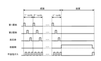
- FIG. 4 is a diagram showing a processing sequence in the first aspect of the present disclosure.
- FIG. 5 is a diagram showing a processing sequence in the second aspect of the present disclosure.
- the processing furnace 202 of the processing apparatus has a heater 207 as a temperature adjustment unit (heating unit).
- the heater 207 is cylindrical and is installed vertically by being supported by a holding plate.
- the heater 207 also functions as an activation mechanism (excitation unit) that activates (excites) the gas by heat.
- a reaction tube 203 is disposed concentrically with the heater 207 inside the heater 207.
- the reaction tube 203 is made of a heat-resistant material such as quartz (SiO 2 ) or silicon carbide (SiC) and is formed in a cylindrical shape with a closed upper end and an open lower end.
- a manifold 209 is disposed concentrically with the reaction tube 203 below the reaction tube 203.
- the manifold 209 is made of a metal material such as stainless steel (SUS) and is formed in a cylindrical shape with an open upper end and a closed lower end. The upper end of the manifold 209 is engaged with the lower end of the reaction tube 203 and is configured to support the reaction tube 203.
- An O-ring 220a is provided between the manifold 209 and the reaction tube 203 as a seal member.
- the reaction tube 203 is installed vertically like the heater 207.
- the reaction tube 203 and the manifold 209 mainly constitute a processing vessel (reaction vessel).
- a processing chamber 201 is formed in a cylindrical hollow portion of the processing vessel.
- the processing chamber 201 is configured to be capable of accommodating a wafer 200 as a substrate. In the processing chamber 201, processing of the wafer 200 is performed.
- Nozzles 249a to 249c serving as first to third supply units are provided within the processing chamber 201, penetrating the sidewall of the manifold 209, respectively. Nozzles 249a to 249c are also referred to as first to third nozzles, respectively. Nozzles 249a to 249c are made of a heat-resistant material such as quartz or SiC. Gas supply pipes 232a to 232c are connected to nozzles 249a to 249c, respectively. Nozzles 249a to 249c are different nozzles, and each of nozzles 249a, 249c is provided adjacent to nozzle 249b.
- Gas supply pipes 232a to 232c are provided with mass flow controllers (MFCs) 241a to 241c, which are flow rate control devices (flow rate control parts), and valves 243a to 243c, which are on-off valves, in order from the upstream side of the gas flow.
- MFCs mass flow controllers
- Gas supply pipes 232d and 232f are connected downstream of valve 243a of gas supply pipe 232a.
- Gas supply pipe 232g is connected downstream of valve 243b of gas supply pipe 232b.
- Gas supply pipes 232e and 232h are connected downstream of valve 243c of gas supply pipe 232c.
- Gas supply pipes 232d to 232h are provided with MFCs 241d to 241h and valves 243d to 243h, in order from the upstream side of the gas flow.
- Gas supply pipes 232a to 232h are made of a metal material, such as SUS.
- the nozzles 249a to 249c are provided in a circular space between the inner wall of the reaction tube 203 and the wafer 200 in a plan view, from the lower part to the upper part of the inner wall of the reaction tube 203, so as to rise upward in the arrangement direction of the wafer 200. That is, the nozzles 249a to 249c are provided in a region horizontally surrounding the wafer arrangement region on the side of the wafer arrangement region in which the wafers 200 are arranged, so as to extend along the wafer arrangement region. In a plan view, the nozzle 249b is arranged to face the exhaust port 231a (described later) in a straight line across the center of the wafer 200 in the processing chamber 201.
- the nozzles 249a and 249c are arranged to sandwich a straight line L passing through the nozzle 249b and the center of the exhaust port 231a from both sides along the inner wall of the reaction tube 203 (the outer periphery of the wafer 200).
- the straight line L is also a straight line passing through the nozzle 249b and the center of the wafer 200.
- nozzle 249c is provided on the opposite side of nozzle 249a across line L.
- Nozzles 249a and 249c are arranged symmetrically with line L as the axis of symmetry.
- Gas supply holes 250a to 250c for supplying gas are provided on the side surfaces of nozzles 249a to 249c, respectively. Each of gas supply holes 250a to 250c opens so as to face exhaust port 231a in plan view, making it possible to supply gas toward wafer 200.
- a plurality of gas supply holes 250a to 250c are provided from the bottom to the top of reaction tube 203.
- raw materials having substructures X and Y are supplied into the processing chamber 201 via the MFC 241a, the valve 243a, and the nozzle 249a.
- the second raw material having partial structure Y is supplied from gas supply pipe 232b into processing chamber 201 via MFC 241b, valve 243b, and nozzle 249b.
- the reactant is supplied from the gas supply pipe 232c into the processing chamber 201 via the MFC 241c, the valve 243c, and the nozzle 249c.
- the first raw material having partial structure X is supplied from gas supply pipe 232d into processing chamber 201 via MFC 241d, valve 243d, gas supply pipe 232a, and nozzle 249a.
- the modifier is supplied from the gas supply pipe 232e into the processing chamber 201 via the MFC 241e, the valve 243e, the gas supply pipe 32c, and the nozzle 249c.
- Inert gas is supplied from gas supply pipes 232f-232h into the processing chamber 201 via MFCs 241f-241h, valves 243f-243h, gas supply pipes 232a-232c, and nozzles 249a-249c.
- the inert gas acts as a purge gas, carrier gas, dilution gas, etc.
- the raw material supply system is mainly composed of gas supply pipe 232a, MFC 241a, and valve 243a.
- the first raw material supply system is mainly composed of gas supply pipe 232d, MFC 241d, and valve 243d.
- the second raw material supply system is mainly composed of gas supply pipe 232b, MFC 241b, and valve 243b.
- the raw material supply system, first raw material supply system, and second raw material supply system may each or all be referred to as the raw material supply system.
- the reactant supply system is mainly composed of gas supply pipe 232c, MFC 241c, and valve 243c.
- the modifier exposure system (modifier supply system) is mainly composed of gas supply pipe 232e, MFC 241e, and valve 243e.
- the inert gas supply system is mainly composed of gas supply pipes 232f-232h, MFCs 241f-241h, and valves 243f-243h.
- any or all of the various supply systems described above may be configured as an integrated supply system 248 in which the valves 243a to 243h and the MFCs 241a to 241h are integrated.
- the integrated supply system 248 is connected to each of the gas supply pipes 232a to 232h, and the supply operation of various substances (various gases) into the gas supply pipes 232a to 232h, i.e., the opening and closing operation of the valves 243a to 243h and the flow rate adjustment operation by the MFCs 241a to 241h, are controlled by a controller 121, which will be described later.
- the integrated supply system 248 is configured as an integrated or separate integrated unit, and can be attached and detached from the gas supply pipes 232a to 232h, etc., in units of integrated units, and is configured so that maintenance, replacement, expansion, etc. of the integrated supply system 248 can be performed in units of integrated units.
- An exhaust port 231a for exhausting the atmosphere in the processing chamber 201 is provided at the bottom of the side wall of the reaction tube 203. As shown in FIG. 2, the exhaust port 231a is provided at a position facing the nozzles 249a to 249c (gas supply holes 250a to 250c) across the wafer 200 in a plan view. The exhaust port 231a may be provided along the side wall of the reaction tube 203 from the bottom to the top, that is, along the wafer arrangement area. An exhaust pipe 231 is connected to the exhaust port 231a.
- a vacuum pump 246 as a vacuum exhaust device is connected to the exhaust pipe 231 via a pressure sensor 245 as a pressure detector (pressure detection unit) that detects the pressure in the processing chamber 201 and an APC (Auto Pressure Controller) valve 244 as a pressure regulator (pressure adjustment unit).
- the APC valve 244 is configured to be able to evacuate and stop the evacuation of the processing chamber 201 by opening and closing the valve while the vacuum pump 246 is operating, and further, to be able to adjust the pressure inside the processing chamber 201 by adjusting the valve opening based on pressure information detected by the pressure sensor 245 while the vacuum pump 246 is operating.
- An exhaust system is mainly configured by the exhaust pipe 231, the APC valve 244, and the pressure sensor 245.
- the vacuum pump 246 may be included in the exhaust system.
- a seal cap 219 is provided as a furnace port cover body capable of airtightly closing the lower end opening of the manifold 209.
- the seal cap 219 is made of a metal material such as SUS and is formed in a disk shape.
- An O-ring 220b is provided on the upper surface of the seal cap 219 as a sealing member that abuts against the lower end of the manifold 209.
- a rotation mechanism 267 is installed to rotate the boat 217 described later.
- the rotation shaft 255 of the rotation mechanism 267 is connected to the boat 217 through the seal cap 219.
- the rotation mechanism 267 is configured to rotate the wafers 200 by rotating the boat 217.
- the seal cap 219 is configured to be raised and lowered vertically by a boat elevator 115 as a lifting mechanism installed outside the reaction tube 203.
- the boat elevator 115 is configured as a transport device (transport mechanism) that transports the wafers 200 in and out of the processing chamber 201 by raising and lowering the seal cap 219.
- a shutter 219s is provided as a furnace port cover that can airtightly close the lower end opening of the manifold 209 when the seal cap 219 is lowered and the boat 217 is removed from the processing chamber 201.
- the shutter 219s is made of a metal material such as SUS and is formed in a disk shape.
- An O-ring 220c is provided on the upper surface of the shutter 219s as a sealing member that abuts against the lower end of the manifold 209.
- the opening and closing operation of the shutter 219s (lifting and lowering operation, rotating operation, etc.) is controlled by a shutter opening and closing mechanism 115s.
- the boat 217 as a substrate support is configured to support multiple wafers 200, for example 25 to 200, in a horizontal position and aligned vertically with their centers aligned, i.e., arranged at intervals, in multiple stages.
- the boat 217 is made of a heat-resistant material such as quartz or SiC.
- insulating plates 218 made of a heat-resistant material such as quartz or SiC are supported in multiple stages.
- a temperature sensor 263 is installed inside the reaction tube 203 as a temperature detector. By adjusting the power supply to the heater 207 based on the temperature information detected by the temperature sensor 263, the temperature inside the processing chamber 201 is distributed as desired.
- the temperature sensor 263 is installed along the inner wall of the reaction tube 203.
- the controller 121 which is a control unit (control means), is configured as a computer equipped with a CPU (Central Processing Unit) 121a, a RAM (Random Access Memory) 121b, a storage device 121c, and an I/O port 121d.
- the RAM 121b, the storage device 121c, and the I/O port 121d are configured to be able to exchange data with the CPU 121a via an internal bus 121e.
- An input/output device 122 configured as, for example, a touch panel is connected to the controller 121.
- an external storage device 123 can be connected to the controller 121.
- the processing device may be configured to have one control unit or multiple control units.
- control for performing the processing sequence described below may be performed using one control unit or multiple control units.
- the multiple control units may be configured as a control system connected to each other via a wired or wireless communication network, and the control for carrying out the processing sequence described below may be performed by the entire control system.
- control unit may include one control unit, multiple control units, or a control system configured by multiple control units.
- the storage device 121c is composed of, for example, a flash memory, a HDD (Hard Disk Drive), an SSD (Solid State Drive), etc.
- a control program for controlling the operation of the processing device, a process recipe describing the procedures and conditions of the substrate processing described later, etc. are recorded and stored in a readable manner.
- the process recipe is a combination of the procedures in the substrate processing described later, which are executed by the controller 121 in the processing device, so that a predetermined result can be obtained, and functions as a program.
- the process recipe, the control program, etc. are collectively referred to simply as a program.
- the process recipe is also simply referred to as a recipe.
- the word program is used in this specification, it may include only a recipe, only a control program, or both.
- the RAM 121b is configured as a memory area (work area) in which the programs and data read by the CPU 121a are temporarily stored.
- the I/O port 121d is connected to the above-mentioned MFCs 241a to 241h, valves 243a to 243h, pressure sensor 245, APC valve 244, vacuum pump 246, temperature sensor 263, heater 207, rotation mechanism 267, boat elevator 115, shutter opening/closing mechanism 115s, etc.
- the CPU 121a is configured to read and execute a control program from the storage device 121c, and to read a recipe from the storage device 121c in response to input of an operation command from the input/output device 122, etc.
- the CPU 121a is configured to control the flow rate adjustment of various substances (various gases) by the MFCs 241a to 241h, the opening and closing of the valves 243a to 243h, the opening and closing of the APC valve 244 and the pressure adjustment by the APC valve 244 based on the pressure sensor 245, the start and stop of the vacuum pump 246, the temperature adjustment of the heater 207 based on the temperature sensor 263, the rotation and rotation speed adjustment of the boat 217 by the rotation mechanism 267, the raising and lowering of the boat 217 by the boat elevator 115, the opening and closing of the shutter 219s by the shutter opening and closing mechanism 115s, etc.
- the controller 121 can be configured by installing the above-mentioned program recorded and stored in the external storage device 123 into a computer.
- the external storage device 123 includes, for example, a magnetic disk such as an HDD, an optical disk such as a CD, a magneto-optical disk such as an MO, and a semiconductor memory such as a USB memory or an SSD.
- the storage device 121c and the external storage device 123 are configured as computer-readable recording media. Hereinafter, these are collectively referred to as recording media.
- recording medium When the term recording medium is used in this specification, it may include only the storage device 121c alone, only the external storage device 123 alone, or both.
- the program may be provided to the computer using a communication means such as the Internet or a dedicated line, without using the external storage device 123.
- processing apparatus is also referred to as a substrate processing apparatus, a film forming processing apparatus, or a film forming apparatus.
- the processing method is also referred to as a substrate processing method, a film forming processing method, or a film forming method.
- a cycle including a step of supplying a raw material having substructures X and Y to wafer 200 (raw material supply step) and a step of supplying a reactant to wafer 200 (reactant supply step) is performed a predetermined number of times (n times, n is an integer of 1 or 2 or more) in the film formation step.
- wafer used in this specification can mean the wafer itself, or a laminate of the wafer and a specified layer or film formed on its surface.
- surface of a wafer used in this specification can mean the surface of the wafer itself, or the surface of a specified layer, etc. formed on the wafer.
- raw material include at least one of gaseous and liquid substances.
- Liquid substances include mist substances.
- each of the raw material, reactant, and modifier may contain a gaseous substance, a liquid substance such as a mist substance, or both.
- the term "layer” includes at least one of a continuous layer and a discontinuous layer.
- the first layer and the second layer may each include a continuous layer, a discontinuous layer, or both.
- the inside of the processing chamber 201 i.e., the space in which the wafer 200 is present, is evacuated (reduced pressure exhaust) by the vacuum pump 246 so that the inside of the processing chamber 201 is at a desired pressure (vacuum level).
- the pressure inside the processing chamber 201 is measured by the pressure sensor 245, and the APC valve 244 is feedback-controlled based on the measured pressure information.
- the wafer 200 inside the processing chamber 201 is heated by the heater 207 so that the wafer 200 is at a desired processing temperature.
- the power supply to the heater 207 is feedback-controlled based on the temperature information detected by the temperature sensor 263 so that the inside of the processing chamber 201 has a desired temperature distribution.
- the rotation mechanism 267 starts rotating the wafer 200. The evacuation inside the processing chamber 201 and the heating and rotation of the wafer 200 are all continued at least until the processing of the wafer 200 is completed.
- a raw material (raw material gas) is supplied to the wafer 200 .
- valve 243a is opened to allow the raw material to flow into gas supply pipe 232a.
- the raw material has its flow rate adjusted by MFC 241a, is supplied into processing chamber 201 via nozzle 249a, and is exhausted from exhaust port 231a.
- the raw material is supplied to wafer 200 from the side of wafer 200 (raw material supply).
- valves 243f to 243h may be opened to supply an inert gas into processing chamber 201 via nozzles 249a to 249c, respectively.
- the processing conditions when supplying the raw material in the raw material supply step are as follows: Treatment temperature: room temperature to 700°C, preferably 60 to 600°C Treatment pressure: 1 to 2666 Pa, preferably 10 to 1333 Pa Raw material supply flow rate: 10 to 10,000 sccm, preferably 100 to 2,000 sccm Raw material supply time: 1 to 240 seconds, preferably 5 to 120 seconds Inert gas supply flow rate (per gas supply pipe): 0 to 20,000 sccm Examples include:
- the process temperature means the temperature of the wafer 200 or the temperature inside the process chamber 201
- the process pressure means the pressure inside the process chamber 201.
- the process time means the time that the process continues.
- the supply flow rate includes 0 sccm
- 0 sccm means that the substance (gas) is not supplied.
- a substance (gas) having partial structure X and partial structure Y can be used as a raw material.
- the partial structure X includes, for example, at least one of Si-CH 2 -Si, Si-CH 2 -CH 2 -Si, Si-R, N(SiR ' 3 ) 3 and CSi 3 H.
- the partial structure Y includes, for example, at least one of Si-OR', Si-NR'-Si, Si-NR' 2 , NR' 3 , Si-Cl, Si-Br, Si-I, B-Cl, B-Br, B-I and Si-H.
- Si stands for silicon
- C stands for carbon
- H stands for hydrogen
- N stands for nitrogen
- O stands for oxygen
- B stands for boron
- Cl stands for chlorine
- Br stands for bromine
- I stands for iodine.
- R represents an alkyl group, and each of the R' groups independently represents a hydrogen atom or an alkyl group.
- the alkyl group is preferably an alkyl group having 1 to 5 carbon atoms, and more preferably an alkyl group having 1 to 4 carbon atoms.
- the alkyl group may be linear or branched. Examples of the alkyl group include a methyl group, an ethyl group, an n-propyl group, an n-butyl group, an isopropyl group, an isobutyl group, a sec-butyl group, and a tert-butyl group.
- OR' represents an alkoxy group.
- the alkoxy group is preferably an alkoxy group having 1 to 5 carbon atoms, and more preferably an alkoxy group having 1 to 4 carbon atoms.
- the alkyl group in the alkoxy group represented by OR' is the same as the alkyl group described above.
- NR'2 represents an amino group.
- the amino group is preferably an amino group having 1 to 5 carbon atoms, and more preferably an amino group having 1 to 4 carbon atoms.
- the alkyl group in the amino group represented by NR'2 is the same as the alkyl group described above.
- the multiple R's may be the same or different.
- a Si-containing substance such as H 3 Si—CH 2 —CH 2 —SiH 2 OR′ gas, N(SiH 3 ) 2 (SiH 2 OR′) gas, N(SiH 3 ) 2 SiH 2 NR′ 2 gas, etc.
- a Si-containing substance such as H 3 Si—CH 2 —CH 2 —SiH 2 OR′ gas, N(SiH 3 ) 2 (SiH 2 OR′) gas, N(SiH 3 ) 2 SiH 2 NR′ 2 gas, etc.
- a Si-containing substance such as H 3 Si—CH 2 —CH 2 —SiH 2 OR′ gas, N(SiH 3 ) 2 (SiH 2 OR′) gas, N(SiH 3 ) 2 SiH 2 NR′ 2 gas, etc.
- one or more of these can be used.
- N2 gas or a rare gas such as argon (Ar) gas, helium (He) gas, neon (Ne) gas, or xenon (Xe) gas can be used.
- Ar argon
- He helium
- Ne neon
- Xe xenon
- the inert gas one or more of these can be used. This also applies to each step described later.
- valve 243a is closed to stop the supply of raw materials into the processing chamber 201. Then, the processing chamber 201 is evacuated to remove gaseous substances remaining in the processing chamber 201 from the processing chamber 201. At this time, valves 243f to 243h are opened to supply an inert gas into the processing chamber 201 through nozzles 249a to 249c. The inert gas supplied from nozzles 249a to 249c acts as a purge gas, thereby purging the processing chamber 201 (purge). It is preferable that the processing temperature when purging in this step is the same as the processing temperature when the raw materials are supplied.
- reactant Supply Step After the raw material supply step is completed, a reactant (reaction gas) is supplied to the wafer 200, that is, the wafer 200 after the first layer is formed on the surface thereof.
- valve 243c is opened to allow reactants to flow into gas supply pipe 232c.
- the reactants are adjusted in flow rate by MFC 241c, supplied into processing chamber 201 via nozzle 249c, and exhausted from exhaust port 231a.
- reactants are supplied to wafer 200 from the side of wafer 200 (reactant supply).
- valves 243f to 243h may be opened to supply an inert gas into processing chamber 201 via nozzles 249a to 249c, respectively.
- the process conditions for supplying the reactants in the reactant supply step are as follows: Treatment pressure: 1 to 13332 Pa, preferably 10 to 1333 Pa Reactant supply flow rate: 10-10000 sccm, preferably 100-2000 sccm Reactant supply time: 1 to 240 seconds, preferably 5 to 120 seconds Other processing conditions may be the same as those in the raw material supply step.
- the reactant may be, for example, an oxygen (O)-containing substance (gas).
- O-containing substance examples include O2 gas, O3 gas, N2O gas, NO2 gas, NO gas, CO2 gas, and CO gas.
- the reactant may be, for example, a nitrogen (N) and hydrogen (H)-containing substance (gas).
- N and H-containing substance include NH3 gas, N2H2 gas , N2H4 gas , and N3H8 gas.
- One or more of these can be used as reactants.
- the valve 243c is closed to stop the supply of reactants into the processing chamber 201. Then, gaseous substances remaining in the processing chamber 201 are removed from the processing chamber 201 (purging) using the same processing procedure and processing conditions as the purging in the raw material supply step. It is preferable that the processing temperature when purging in this step is the same as the processing temperature when supplying the reactants.
- the above-mentioned raw material supply step and reactant supply step are performed asynchronously, i.e., by performing a cycle of n times (n is an integer of 1 or 2 or more) in this order, it is possible to form a first film on the surface of the wafer 200. It is preferable to repeat the above-mentioned cycle multiple times. That is, it is preferable to make the thickness of the second layer formed per cycle thinner than the desired film thickness, and to repeat the above-mentioned cycle multiple times until the film thickness of the first film formed by stacking the second layers reaches the desired film thickness.
- Si-containing material When the above-mentioned Si-containing material is used as a raw material and the above-mentioned O-containing material is used as a reactant, a film containing Si and O, i.e., a silicon oxide film (SiO film), is formed on the surface of the wafer 200.
- SiO film silicon oxide film
- N- and H-containing material When the above-mentioned Si-containing material is used as a raw material and the above-mentioned N- and H-containing material is used as a reactant, a film containing Si and N, i.e., a silicon nitride film (SiN film), is formed on the surface of the wafer 200.
- SiN film silicon nitride film
- the first film will be a film containing at least a portion of partial structure X and partial structure Z derived from partial structure Y.
- the partial structure X includes at least one of, for example, Si-CH 2 -Si, Si-CH 2 -CH 2 -Si, Si-R, N(SiR ' 3 ) 3 and CSi 3 H.
- the first film may include Si-CH 2 -Si itself as at least a part of the partial structure X, or may include a structure in which a specific atom has been removed from the partial structure X, such as Si-CH 2.
- the first film may include Si-CH 2 -CH 2 -Si itself as at least a part of the partial structure X, or may include a structure in which a specific atom has been removed from the partial structure X, such as Si-CH 2 -CH 2 or Si-CH 2 .
- Substructure Z is a structure derived from substructure Y.
- Substructure Z can be said to be a structure generated in the process of a raw material having substructure Y chemically reacting with the surface of the wafer 200, or in other words, a structure generated in the process of a raw material having substructure Y being thermally decomposed.
- Substructure Z may have the same chemical structure as substructure Y. That is, substructure Z may be obtained by incorporating substructure Y directly into the first film.
- Substructure Z may also be generated by altering substructure Y. That is, substructure Z may be generated by changing at least one of the composition and chemical structure of substructure Y. For these reasons, substructure Y can be said to be a structure that is the source of generating substructure Z in the first film.
- the partial structure Y includes at least one of, for example, Si-OR', Si-NR'-Si, Si-NR' 2 , NR' 3 , Si-Cl, Si-Br, Si-I, B-Cl, B-Br, B-I, and Si-H. Therefore, the partial structure Z derived from the partial structure Y includes at least one of, for example, Si-OR', Si-NR'-Si, Si-NR' 2 , Si-Cl, Si-Br, Si-I, B-Cl, B-Br, B-I, and Si-H.
- the first film may include Si-NR'-Si itself as the partial structure Z derived from the partial structure Y, or may include a structure in which Si and R' are replaced, such as Si-NR' 2 .
- the first film may contain Si— NR′2 itself as the partial structure Z derived from the partial structure Y, or may contain a structure in which R′ is replaced by Si, such as Si—NR′-Si.
- Modification step Thereafter, a subsequent modifier exposure step is performed.
- the film formed on the surface of the wafer 200 that is, the first film including at least a part of the substructure X and the substructure Z derived from the substructure Y, is exposed to a modifying agent.
- valve 243e is opened to allow the modifying agent to flow into gas supply pipe 232e.
- the flow rate of the modifying agent is adjusted by MFC 241e, and the modifying agent is supplied into processing chamber 201 via gas supply pipe 232c and nozzle 249c, and exhausted from exhaust port 231a.
- the modifying agent is supplied to wafer 200 from the side of wafer 200, and the first film formed on the surface of wafer 200 is exposed to the modifying agent, causing the first film to react with the modifying agent (modifying agent exposure).
- valves 243f to 243h may be opened to supply an inert gas into processing chamber 201 via nozzles 249a to 249c, respectively.
- This step is preferably carried out under conditions in which the reactivity of the partial structure Z contained in the first film with the modifier is higher than the reactivity of at least a portion of the partial structure X contained in the first film with the modifier.
- this step is preferably performed under conditions that allow at least a portion of the substructure X contained in the first film to be maintained.
- this step is preferably performed under conditions that make it possible to change at least one of the composition and chemical structure of at least a part of the partial structure Z contained in the first film.
- this step is preferably performed under conditions that make it possible to change at least a part of the partial structure Z contained in the first film to a different partial structure V.
- the number of elements constituting the partial structure V may be less than the number of elements constituting the partial structure Z.
- this step is preferably performed under conditions that make it possible to remove at least one of the elements constituting the partial structure Z contained in the first film and/or replace it with another element.
- the case of removing at least one of the elements constituting the partial structure Z contained in the first film includes the case of removing one element, the case of removing multiple elements, and the case of removing all elements, among the elements constituting the partial structure Z.
- the partial structure Z is Si-OR'
- this case includes the case of removing Si, removing R', and removing Si-OR' itself, among the elements constituting the partial structure Z.
- the partial structure Z is Si-NR'-Si
- this case includes the case of removing Si, removing R', and removing Si-NR'-Si itself, among the elements constituting the partial structure Z.
- cases other than the case of removing the partial structure Z itself are examples of changing the composition of at least a part of the partial structure Z, and are also examples of changing the chemical structure of at least a part of the partial structure Z.
- cases other than the case of removing the partial structure Z itself are examples of changing at least a part of the partial structure Z to a different partial structure V, and are also examples in which the number of elements constituting the partial structure V is less than the number of elements constituting the partial structure Z.
- the structure remaining after removing at least one of the elements that make up substructure Z is substructure V.
- the case where at least one of the elements constituting the partial structure Z contained in the first film is replaced with another element includes the case where one element of the elements constituting the partial structure Z is replaced with another element, the case where multiple elements are replaced with other elements, and the case where all elements are replaced with other elements.
- the partial structure Z is Si-OR'
- this case includes the case where, among the elements constituting the partial structure Z, Si is replaced with R', R' is replaced with Si, and Si-OR' itself is replaced with another element.
- the partial structure Z is Si-NR'-Si
- this case includes the case where, among the elements constituting the partial structure Z, Si is replaced with R', R' is replaced with Si, and Si-NR'-Si itself is replaced with another element.
- the processing conditions for supplying the modifier in the modifier exposure step are as follows: Treatment pressure: 1 to 100,000 Pa, preferably 100 to 100,000 Pa Modifier supply flow rate: 10 to 10,000 sccm, preferably 100 to 2,000 sccm Modifier supply time: 1 to 300 minutes, preferably 10 to 240 minutes. Other processing conditions may be the same as those used when supplying the raw material in the raw material supply step.
- H and O 2 gas for example, a hydrogen (H) and oxygen (O) containing substance (gas) can be used.
- H and O containing substance for example, H 2 O gas, H 2 O 2 gas, H 2 gas + O 2 gas, D 2 gas + O 2 gas, H 2 gas + O 3 gas, D 2 gas + O 3 gas, etc.
- D represents deuterium.
- H 2 gas + O 2 gas means a mixed gas of H 2 gas and O 2 gas.
- the two gases When supplying a mixed gas, the two gases may be mixed (premixed) in a supply pipe and then supplied into the processing chamber 201, or the two gases may be supplied separately from different supply pipes into the processing chamber 201 and mixed (postmixed) in the processing chamber 201.
- the modifier one or more of these can be used.
- the first film formed on the surface of the wafer 200 is exposed to the above-mentioned modifier under the above-mentioned processing conditions, thereby making it possible to react the first film with the reactant.
- This makes it possible to modify (change) the first film into a second film that contains at least a part of the partial structure X and has a smaller amount of the partial structure Z than the amount of the partial structure Z contained in the first film.
- This makes it possible to change the first film into a second film having a density lower than that of the first film.
- this step it may be possible to change at least a part of the partial structure Z contained in the first film into a partial structure containing Si-O-Si, i.e., a partial structure containing siloxane, which makes it possible to further reduce the density of the first film.
- the second film becomes a film containing siloxane bonds.
- the valve 243e is closed to stop the supply of the modifier into the processing chamber 201. Then, gaseous substances remaining in the processing chamber 201 are removed from the processing chamber 201 using the same processing procedures and conditions as the purging in the raw material supply step (purging).
- the processing temperature when purging in this step is preferably the same as the processing temperature in the modifier exposure step.
- an inert gas is supplied as a purge gas from each of the nozzles 249a to 249c into the processing chamber 201, and exhausted from the exhaust port 231a. This purges the processing chamber 201, and gases and reaction by-products remaining in the processing chamber 201 are removed from the processing chamber 201 (after-purge). Thereafter, the atmosphere in the processing chamber 201 is replaced with the inert gas (inert gas replacement), and the pressure in the processing chamber 201 is returned to normal pressure (atmospheric pressure return).
- the seal cap 219 is lowered by the boat elevator 115, and the lower end of the manifold 209 is opened. Then, the processed wafers 200 are carried out from the lower end of the manifold 209 to the outside of the reaction tube 203 while being supported by the boat 217 (boat unloading). After the boat unloading, the shutter 219s is moved, and the lower end opening of the manifold 209 is sealed by the shutter 219s via the O-ring 220c (shutter close). After being carried out to the outside of the reaction tube 203, the processed wafers 200 are taken out of the boat 217 (wafer discharge).
- the amount of partial structure Z contained in the second film can be effectively reduced compared to the amount of partial structure Z contained in the first film, and the density of the second film can be effectively reduced and the k value of the second film can be effectively reduced. That is, the low-k nature of the second film can be effectively realized.
- the number of elements constituting the partial structure V may be less than the number of elements constituting the partial structure Z, which makes it possible to more effectively reduce the density of the second film and the k value of the second film. That is, the low-k nature of the second film can be effectively realized.
- the partial structure X includes at least one of Si-CH 2 -Si, Si-CH 2 -CH 2 -Si, Si-R, N(SiR ' 3 ) 3 and CSi 3 H
- the partial structure Y includes at least one of Si-OR', Si-NR'-Si, Si-NR' 2 , NR' 3 , Si-Cl, Si-Br, Si-I, B-Cl, B-Br, B-I and Si-H
- the partial structure Z includes at least one of Si-OR', Si-NR'-Si, Si-NR' 2 , Si-Cl, Si-Br, Si-I, B-Cl, B-Br, B-I and Si-H, thereby making it possible to effectively cause the above-mentioned reaction.
- partial structure Z has the same chemical structure as partial structure Y, i.e., partial structure Z is obtained by incorporating partial structure Y into the first film, it is possible to effectively cause the above-mentioned reaction.
- the partial structure Z is generated by altering the partial structure Y, i.e., the partial structure Z is generated by changing at least one of the composition and chemical structure of the partial structure Y, thereby making it possible to effectively cause the above-mentioned reaction.
- the processing sequence in this embodiment differs from the first embodiment described above in that a first source material having a partial structure X and a second source material having a partial structure Y are supplied in the film formation step. Other points are the same as those in the first embodiment.
- a cycle including a step of supplying a first source having a substructure X to the wafer 200 (first source supply step), a step of supplying a second source having a substructure Y to the wafer 200 (second source supply step), and a step of supplying a reactant to the wafer 200 (reactant supply step) is performed a predetermined number of times (n times, n is an integer of 1 or 2 or more) in the film formation step.
- valve 243d is opened and the first raw material is flowed into gas supply pipe 232d.
- the flow rate of the first raw material is adjusted by MFC 241d, and the first raw material is supplied into processing chamber 201 via gas supply pipe 232a and nozzle 249a, and exhausted from exhaust port 231a.
- the first raw material is supplied to wafer 200 from the side of wafer 200 (first raw material supply).
- valves 243f to 243h may be opened to supply an inert gas into processing chamber 201 via each of nozzles 249a to 249c.
- the processing conditions for supplying the first raw material in the first raw material supplying step are as follows: First raw material supply flow rate: 10 to 10,000 sccm, preferably 100 to 2,000 sccm First raw material supply time: 1 to 240 seconds, preferably 5 to 120 seconds. Other processing conditions can be the same as the processing conditions when the raw material is supplied in the raw material supply step of the first embodiment.
- a substance (gas) having at least one of the partial structures X exemplified in the first embodiment for example, Si-CH 2 -Si, Si-CH 2 -CH 2 -Si, Si-R, N(SiR' 3 ) 3 , and CSi 3 H, can be used.
- the first raw material for example, SiH 3 CH 2 SiH 3 gas, SiH 3 CH 2 CH 2 SiH 3 gas, SiH 2 (CH 3 ) 2 gas, and N(SiH 3 ) 3 gas can be used.
- SiH 3 CH 2 SiH 3 gas SiH 3 CH 2 CH 2 SiH 3 gas
- SiH 2 (CH 3 ) 2 gas, and N(SiH 3 ) 3 gas can be used.
- one or more of these can be used.
- valve 243d is closed to stop the supply of the first raw material into processing chamber 201. Then, gaseous substances remaining in processing chamber 201 are removed from processing chamber 201 (purging) using the same processing procedures and conditions as the purging in the raw material supply step of the first embodiment. It is preferable that the processing temperature when purging in this step is the same as the processing temperature when supplying the first raw material.
- valve 243b is opened to allow the second raw material to flow into gas supply pipe 232b.
- the flow rate of the second raw material is adjusted by MFC 241b, and the second raw material is supplied into processing chamber 201 via nozzle 249b and exhausted from exhaust port 231a.
- the second raw material is supplied to wafer 200 from the side of wafer 200 (second raw material supply).
- valves 243f to 243h may be opened to supply an inert gas into processing chamber 201 via nozzles 249a to 249c, respectively.
- the processing conditions for supplying the second raw material in the second raw material supplying step are as follows: Second raw material supply flow rate: 10 to 10,000 sccm, preferably 100 to 2,000 sccm Second raw material supply time: 1 to 240 seconds, preferably 5 to 120 seconds. Other processing conditions can be the same as the processing conditions when the raw material is supplied in the raw material supply step of the first embodiment.
- a substance (gas) having at least one of the partial structure Y exemplified in the first embodiment for example, Si-OR', Si-NR'-Si, Si- NR'2 , NR'3 , Si-Cl, Si-Br, Si-I, B-Cl, B-Br, B-I, and Si-H
- Si-OR' Si-NR'-Si, Si- NR'2 , NR'3 , Si-Cl, Si-Br, Si-I, B-Cl, B-Br, B-I, and Si-H
- Si-OR' for example, H3Si - CH2 - CH2 -SiH2OR' gas, ( CH3 ) 3SiNHSi ( CH3 ) 3 gas, N ( SiH3 ) 2SiH2NR'2 gas, NH3 gas, and Si3Cl8 gas can be used.
- one or more of these can be used.
- valve 243b is closed to stop the supply of the second raw material into processing chamber 201. Then, gaseous substances remaining in processing chamber 201 are removed from processing chamber 201 (purging) using the same processing procedures and conditions as the purging in the raw material supply step of the first embodiment. It is preferable that the processing temperature when purging in this step is the same as the processing temperature when the second raw material is supplied.
- the process procedure and process conditions in the reactant supply step of the second embodiment can be the same as those in the reactant supply step of the first embodiment.
- Substructure Z derived from substructure Y includes at least one of, for example, Si-OR', Si-NR'-Si, Si-NR' 2 , Si-Cl, Si-Br, Si-I, B-Cl, B-Br, B-I, and Si-H, similar to the first embodiment.
- a modification step is performed, in which the first film formed on the surface of the wafer 200 is exposed to a modifier and reacted with the modifier.
- the processing procedure and processing conditions in the modification step of the second aspect can be the same as those in the modification step of the first aspect.
- the first film it is also possible to modify (change) the first film into a second film that contains at least a part of the partial structure X and has a smaller amount of the partial structure Z than the amount of the partial structure Z contained in the first film.
- This makes it possible to change the first film into a second film having a density lower than that of the first film.
- the second film becomes a porous film.
- the second film becomes a film containing siloxane bonds.
- the same effect as in the first embodiment can be obtained.
- the substrate may be processed according to the processing sequence shown below (n is an integer of 1 or 2 or more).
- n is an integer of 1 or 2 or more.
- the substrate may be processed according to the processing sequence shown below (where m and n are integers of 1 or 2 or more). In these embodiments, the same effects as those in the above embodiment can be obtained.
- a step of supplying a catalyst to the substrate may be performed at the timing of starting each cycle of the film formation step, as shown in the processing sequence shown below (n is an integer of 1 or 2 or more).
- a “catalyst” refers to a substance that does not change itself before and after a chemical reaction, but does change the rate of the reaction.
- the catalyst in the reaction system of this embodiment has a catalytic effect that changes the rate of the reaction, but part of the molecular structure may decompose during the reaction process, and the catalyst itself may change before and after the chemical reaction.
- substances that have a catalytic effect that changes the rate of a reaction including those that do not change before and after a chemical reaction, as well as those that may change before and after a chemical reaction, are referred to as catalysts.
- a boron (B)-containing substance gas
- B boron
- BClH2 gas, BCl2H gas, BCl3 gas, BF3 gas, BBr3 gas, and B2H6 gas can be used.
- F represents fluorine.
- the treatment conditions for supplying the catalyst are as follows: Catalyst supply flow rate: 10 to 10,000 sccm, preferably 100 to 2,000 sccm Catalyst supply time: 1 to 240 seconds, preferably 5 to 120 seconds.
- Other treatment conditions may be the same as those used when supplying the raw material in the raw material supply step of the first embodiment.
- the atmosphere may be introduced into the processing chamber, and the modifier exposure step may be performed in the atmosphere.
- the substrate may be removed from the processing chamber, and the modifier exposure step may be performed in the atmosphere.
- oxygen (O 2 ) or moisture (H 2 O) contained in the atmosphere may be used as the modifier. In these cases, the same effects as those of the above-mentioned aspect can be obtained.
- the recipes used for each process are preferably prepared individually according to the process content, and recorded and stored in the storage device 121c via an electric communication line or external storage device 123. Then, when starting each process, the CPU 121a preferably selects an appropriate recipe according to the process content from among the multiple recipes recorded and stored in the storage device 121c. This makes it possible to reproducibly form films of various film types, composition ratios, film qualities, and film thicknesses in the processing device. It also reduces the burden on the operator, and allows each process to be started quickly while avoiding operating errors.
- the above-mentioned recipes do not necessarily have to be created anew, but may be prepared, for example, by modifying an existing recipe that has already been installed in the processing device.
- the modified recipe may be installed in the processing device via a telecommunications line or a recording medium on which the recipe is recorded.
- an existing recipe that has already been installed in the processing device may be directly modified by operating the input/output device 122 provided in the existing processing device.
- an example of forming a film using a batch-type processing apparatus that processes multiple substrates at a time has been described.
- the present disclosure is not limited to the above-mentioned embodiment, and can be suitably applied, for example, to a case where a film is formed using a single-wafer processing apparatus that processes one or several substrates at a time.
- an example of forming a film using a processing apparatus having a hot-wall type processing furnace has been described.
- the present disclosure is not limited to the above-mentioned embodiment, and can be suitably applied to a case where a film is formed using a processing apparatus having a cold-wall type processing furnace.
- each process can be performed using the same processing procedures and conditions as the above-mentioned aspects and modifications, and the same effects as the above-mentioned aspects and modifications can be obtained.
Landscapes
- Chemical & Material Sciences (AREA)
- General Chemical & Material Sciences (AREA)
- Chemical Kinetics & Catalysis (AREA)
- Engineering & Computer Science (AREA)
- Materials Engineering (AREA)
- Mechanical Engineering (AREA)
- Metallurgy (AREA)
- Organic Chemistry (AREA)
- Inorganic Chemistry (AREA)
- Chemical Vapour Deposition (AREA)
Priority Applications (6)
| Application Number | Priority Date | Filing Date | Title |
|---|---|---|---|
| PCT/JP2023/021234 WO2024252586A1 (ja) | 2023-06-07 | 2023-06-07 | 処理方法、半導体装置の製造方法、処理装置、およびプログラム |
| CN202380094229.3A CN120712642A (zh) | 2023-06-07 | 2023-06-07 | 处理方法、半导体装置的制造方法、处理装置以及程序 |
| JP2025525549A JPWO2024252586A1 (enExample) | 2023-06-07 | 2023-06-07 | |
| KR1020257031318A KR20260025074A (ko) | 2023-06-07 | 2023-06-07 | 처리 방법, 반도체 장치의 제조 방법, 처리 장치 및 프로그램 |
| TW113120428A TW202503099A (zh) | 2023-06-07 | 2024-06-03 | 處理方法、半導體裝置之製造方法、處理裝置及程式 |
| US19/332,505 US20260015731A1 (en) | 2023-06-07 | 2025-09-18 | Processing method, method of manufacturing semiconductor device, processing apparatus, and recording medium |
Applications Claiming Priority (1)
| Application Number | Priority Date | Filing Date | Title |
|---|---|---|---|
| PCT/JP2023/021234 WO2024252586A1 (ja) | 2023-06-07 | 2023-06-07 | 処理方法、半導体装置の製造方法、処理装置、およびプログラム |
Related Child Applications (1)
| Application Number | Title | Priority Date | Filing Date |
|---|---|---|---|
| US19/332,505 Continuation US20260015731A1 (en) | 2023-06-07 | 2025-09-18 | Processing method, method of manufacturing semiconductor device, processing apparatus, and recording medium |
Publications (1)
| Publication Number | Publication Date |
|---|---|
| WO2024252586A1 true WO2024252586A1 (ja) | 2024-12-12 |
Family
ID=93795749
Family Applications (1)
| Application Number | Title | Priority Date | Filing Date |
|---|---|---|---|
| PCT/JP2023/021234 Ceased WO2024252586A1 (ja) | 2023-06-07 | 2023-06-07 | 処理方法、半導体装置の製造方法、処理装置、およびプログラム |
Country Status (6)
| Country | Link |
|---|---|
| US (1) | US20260015731A1 (enExample) |
| JP (1) | JPWO2024252586A1 (enExample) |
| KR (1) | KR20260025074A (enExample) |
| CN (1) | CN120712642A (enExample) |
| TW (1) | TW202503099A (enExample) |
| WO (1) | WO2024252586A1 (enExample) |
Citations (6)
| Publication number | Priority date | Publication date | Assignee | Title |
|---|---|---|---|---|
| JP2008091469A (ja) * | 2006-09-29 | 2008-04-17 | Yoshimi Shiotani | 半導体製造装置、半導体製造方法及び電子機器 |
| JP2009111382A (ja) * | 2007-10-22 | 2009-05-21 | Applied Materials Inc | 遠隔プラズマcvdによりジシラン前駆体から高品質シリコン酸化膜を形成する方法 |
| JP2012504867A (ja) * | 2008-10-01 | 2012-02-23 | アプライド マテリアルズ インコーポレイテッド | 窒化ケイ素系膜又は炭化ケイ素系膜を形成する方法 |
| JP2020522133A (ja) * | 2017-05-25 | 2020-07-27 | アプライド マテリアルズ インコーポレイテッドApplied Materials,Incorporated | 窒化ケイ素膜の高圧処理 |
| JP2022529255A (ja) * | 2019-04-16 | 2022-06-20 | アプライド マテリアルズ インコーポレイテッド | トレンチに薄膜を堆積する方法 |
| JP2023504353A (ja) * | 2019-12-09 | 2023-02-03 | アプライド マテリアルズ インコーポレイテッド | 酸素ラジカル支援による誘電体膜の高密度化 |
-
2023
- 2023-06-07 JP JP2025525549A patent/JPWO2024252586A1/ja active Pending
- 2023-06-07 KR KR1020257031318A patent/KR20260025074A/ko active Pending
- 2023-06-07 WO PCT/JP2023/021234 patent/WO2024252586A1/ja not_active Ceased
- 2023-06-07 CN CN202380094229.3A patent/CN120712642A/zh active Pending
-
2024
- 2024-06-03 TW TW113120428A patent/TW202503099A/zh unknown
-
2025
- 2025-09-18 US US19/332,505 patent/US20260015731A1/en active Pending
Patent Citations (6)
| Publication number | Priority date | Publication date | Assignee | Title |
|---|---|---|---|---|
| JP2008091469A (ja) * | 2006-09-29 | 2008-04-17 | Yoshimi Shiotani | 半導体製造装置、半導体製造方法及び電子機器 |
| JP2009111382A (ja) * | 2007-10-22 | 2009-05-21 | Applied Materials Inc | 遠隔プラズマcvdによりジシラン前駆体から高品質シリコン酸化膜を形成する方法 |
| JP2012504867A (ja) * | 2008-10-01 | 2012-02-23 | アプライド マテリアルズ インコーポレイテッド | 窒化ケイ素系膜又は炭化ケイ素系膜を形成する方法 |
| JP2020522133A (ja) * | 2017-05-25 | 2020-07-27 | アプライド マテリアルズ インコーポレイテッドApplied Materials,Incorporated | 窒化ケイ素膜の高圧処理 |
| JP2022529255A (ja) * | 2019-04-16 | 2022-06-20 | アプライド マテリアルズ インコーポレイテッド | トレンチに薄膜を堆積する方法 |
| JP2023504353A (ja) * | 2019-12-09 | 2023-02-03 | アプライド マテリアルズ インコーポレイテッド | 酸素ラジカル支援による誘電体膜の高密度化 |
Also Published As
| Publication number | Publication date |
|---|---|
| JPWO2024252586A1 (enExample) | 2024-12-12 |
| TW202503099A (zh) | 2025-01-16 |
| CN120712642A (zh) | 2025-09-26 |
| KR20260025074A (ko) | 2026-02-23 |
| US20260015731A1 (en) | 2026-01-15 |
Similar Documents
| Publication | Publication Date | Title |
|---|---|---|
| JP7303226B2 (ja) | 基板処理方法、半導体装置の製造方法、基板処理装置、およびプログラム | |
| US20190368036A1 (en) | Method of cleaning, method of manufacturing semiconductor device, substrate processing apparatus, and recording medium | |
| JPWO2018055724A1 (ja) | 半導体装置の製造方法、基板処理装置およびプログラム | |
| CN115110058B (zh) | 半导体装置的制造方法、基板处理方法、记录介质和基板处理装置 | |
| JP7274039B2 (ja) | 基板処理方法、半導体装置の製造方法、基板処理装置、およびプログラム | |
| JP7579959B2 (ja) | 基板処理方法、半導体装置の製造方法、基板処理装置、およびプログラム | |
| JP7189914B2 (ja) | クリーニング方法、半導体装置の製造方法、基板処理装置、およびプログラム | |
| JP7662748B2 (ja) | 基板処理方法、基板処理装置、半導体装置の製造方法、およびプログラム | |
| JP7654610B2 (ja) | 基板処理方法、半導体装置の製造方法、プログラム、および基板処理装置 | |
| US11728162B2 (en) | Method of manufacturing semiconductor device, substrate processing apparatus, and recording medium | |
| JP7138130B2 (ja) | 基板処理方法、半導体装置の製造方法、基板処理装置およびプログラム | |
| WO2024038602A1 (ja) | 基板処理方法、半導体装置の製造方法、基板処理装置、およびプログラム | |
| JP2024047208A (ja) | 基板処理方法、半導体装置の製造方法、基板処理システム、およびプログラム | |
| KR20260025074A (ko) | 처리 방법, 반도체 장치의 제조 방법, 처리 장치 및 프로그램 | |
| JP7537003B2 (ja) | 処理方法、半導体装置の製造方法、処理装置、およびプログラム | |
| US20250006490A1 (en) | Substrate processing method, method of manufacturing semiconductor device, non-transitory computer-readable recording medium and substrate processing apparatus | |
| US20250104998A1 (en) | Processing method, method of manufacturing semiconductor device, processing apparatus, and recording medium | |
| EP4484607A1 (en) | Method of processing substrate, method of manufacturing semiconductor device, program, and substrate processing apparatus | |
| WO2024116592A1 (ja) | 処理方法、半導体装置の製造方法、処理装置、およびプログラム | |
| JP2024136417A (ja) | 基板処理方法、半導体装置の製造方法、プログラム、および基板処理装置 | |
| KR20250129630A (ko) | 기판 처리 방법, 반도체 장치의 제조 방법, 기판 처리 시스템 및 프로그램 | |
| WO2025182671A1 (ja) | 処理方法、処理装置、プログラム、および高純度原料組成物 | |
| JP2026064322A (ja) | 処理方法、半導体装置の製造方法、処理装置、およびプログラム | |
| TW202607799A (zh) | 基板處理方法、半導體裝置之製造方法、程式及基板處理裝置 | |
| JP2026010499A (ja) | 処理方法、半導体装置の製造方法、処理装置、およびプログラム |
Legal Events
| Date | Code | Title | Description |
|---|---|---|---|
| 121 | Ep: the epo has been informed by wipo that ep was designated in this application |
Ref document number: 23940687 Country of ref document: EP Kind code of ref document: A1 |
|
| ENP | Entry into the national phase |
Ref document number: 2025525549 Country of ref document: JP Kind code of ref document: A |
|
| WWE | Wipo information: entry into national phase |
Ref document number: 2025525549 Country of ref document: JP |
|
| NENP | Non-entry into the national phase |
Ref country code: DE |