WO2024247789A1 - 光電変換素子の製造方法および光電変換素子 - Google Patents
光電変換素子の製造方法および光電変換素子 Download PDFInfo
- Publication number
- WO2024247789A1 WO2024247789A1 PCT/JP2024/018543 JP2024018543W WO2024247789A1 WO 2024247789 A1 WO2024247789 A1 WO 2024247789A1 JP 2024018543 W JP2024018543 W JP 2024018543W WO 2024247789 A1 WO2024247789 A1 WO 2024247789A1
- Authority
- WO
- WIPO (PCT)
- Prior art keywords
- photoelectric conversion
- layer
- conversion element
- hole
- gas barrier
- Prior art date
- Legal status (The legal status is an assumption and is not a legal conclusion. Google has not performed a legal analysis and makes no representation as to the accuracy of the status listed.)
- Ceased
Links
Images


Classifications
-
- H—ELECTRICITY
- H10—SEMICONDUCTOR DEVICES; ELECTRIC SOLID-STATE DEVICES NOT OTHERWISE PROVIDED FOR
- H10F—INORGANIC SEMICONDUCTOR DEVICES SENSITIVE TO INFRARED RADIATION, LIGHT, ELECTROMAGNETIC RADIATION OF SHORTER WAVELENGTH OR CORPUSCULAR RADIATION
- H10F77/00—Constructional details of devices covered by this subclass
- H10F77/30—Coatings
- H10F77/306—Coatings for devices having potential barriers
- H10F77/311—Coatings for devices having potential barriers for photovoltaic cells
-
- H—ELECTRICITY
- H10—SEMICONDUCTOR DEVICES; ELECTRIC SOLID-STATE DEVICES NOT OTHERWISE PROVIDED FOR
- H10F—INORGANIC SEMICONDUCTOR DEVICES SENSITIVE TO INFRARED RADIATION, LIGHT, ELECTROMAGNETIC RADIATION OF SHORTER WAVELENGTH OR CORPUSCULAR RADIATION
- H10F19/00—Integrated devices, or assemblies of multiple devices, comprising at least one photovoltaic cell covered by group H10F10/00, e.g. photovoltaic modules
- H10F19/10—Integrated devices, or assemblies of multiple devices, comprising at least one photovoltaic cell covered by group H10F10/00, e.g. photovoltaic modules comprising photovoltaic cells in arrays in a single semiconductor substrate, the photovoltaic cells having vertical junctions or V-groove junctions
-
- H—ELECTRICITY
- H10—SEMICONDUCTOR DEVICES; ELECTRIC SOLID-STATE DEVICES NOT OTHERWISE PROVIDED FOR
- H10F—INORGANIC SEMICONDUCTOR DEVICES SENSITIVE TO INFRARED RADIATION, LIGHT, ELECTROMAGNETIC RADIATION OF SHORTER WAVELENGTH OR CORPUSCULAR RADIATION
- H10F71/00—Manufacture or treatment of devices covered by this subclass
- H10F71/134—Irradiation with electromagnetic or particle radiation
-
- Y—GENERAL TAGGING OF NEW TECHNOLOGICAL DEVELOPMENTS; GENERAL TAGGING OF CROSS-SECTIONAL TECHNOLOGIES SPANNING OVER SEVERAL SECTIONS OF THE IPC; TECHNICAL SUBJECTS COVERED BY FORMER USPC CROSS-REFERENCE ART COLLECTIONS [XRACs] AND DIGESTS
- Y02—TECHNOLOGIES OR APPLICATIONS FOR MITIGATION OR ADAPTATION AGAINST CLIMATE CHANGE
- Y02E—REDUCTION OF GREENHOUSE GAS [GHG] EMISSIONS, RELATED TO ENERGY GENERATION, TRANSMISSION OR DISTRIBUTION
- Y02E10/00—Energy generation through renewable energy sources
- Y02E10/50—Photovoltaic [PV] energy
- Y02E10/549—Organic PV cells
-
- Y—GENERAL TAGGING OF NEW TECHNOLOGICAL DEVELOPMENTS; GENERAL TAGGING OF CROSS-SECTIONAL TECHNOLOGIES SPANNING OVER SEVERAL SECTIONS OF THE IPC; TECHNICAL SUBJECTS COVERED BY FORMER USPC CROSS-REFERENCE ART COLLECTIONS [XRACs] AND DIGESTS
- Y02—TECHNOLOGIES OR APPLICATIONS FOR MITIGATION OR ADAPTATION AGAINST CLIMATE CHANGE
- Y02P—CLIMATE CHANGE MITIGATION TECHNOLOGIES IN THE PRODUCTION OR PROCESSING OF GOODS
- Y02P70/00—Climate change mitigation technologies in the production process for final industrial or consumer products
- Y02P70/50—Manufacturing or production processes characterised by the final manufactured product
Definitions
- This disclosure relates to a method for manufacturing a photoelectric conversion element and a photoelectric conversion element.
- Non-Patent Document 1 there has been active research and development into flexible photoelectric conversion elements in which photoelectric conversion elements are formed on flexible substrates.
- This disclosure provides a method for manufacturing photoelectric conversion elements that produce photoelectric conversion elements that combine high durability with uniformity in appearance.
- the method for producing a photoelectric conversion element includes the steps of: (A) forming a first electrode layer on a gas barrier layer; (B) removing a portion of the first electrode layer using a pulsed laser to form through holes penetrating the first electrode layer such that a portion of a plurality of holes overlaps with one another; (C) forming a light absorbing layer on the first electrode layer and on the gas barrier layer exposed by the through holes; (D) forming a second electrode layer on the light absorbing layer; Includes.
- This disclosure provides a method for manufacturing photoelectric conversion elements that produce photoelectric conversion elements that combine high durability with uniformity in appearance.
- FIG. 1 is a schematic cross-sectional view for explaining a method for manufacturing a photoelectric conversion element according to the first embodiment of the present disclosure.
- FIG. 2 is an explanatory diagram for explaining a method for determining the average value L ave of the line width L of the through hole.
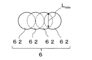
- FIG. 3 is an explanatory diagram for explaining the relationship between the overlap of pulses irradiated to continuously form circular through-holes, the minimum value L min of the line width L of the linear through-holes formed, and the ratio L min /L ave .
- FIG. 4A is a schematic diagram showing a linear through hole having a ratio L min /L ave of 0.57, formed by successively forming circular through holes formed by irradiation with one pulse.
- FIG. 4A is a schematic diagram showing a linear through hole having a ratio L min /L ave of 0.57, formed by successively forming circular through holes formed by irradiation with one pulse.
- FIG. 4B is a schematic diagram showing a linear through hole having a ratio L min /L ave of 0.91, formed by successively forming circular through holes formed by irradiation with one pulse.
- FIG. 5 is a schematic cross-sectional view showing an example of a photoelectric conversion element according to the first embodiment of the present disclosure.
- FIG. 6 is a schematic cross-sectional view showing a modified example of the photoelectric conversion element according to the first embodiment of the present disclosure.
- FIG. 7 is a schematic cross-sectional view showing a photoelectric conversion module which is a photoelectric conversion element according to the second embodiment of the present disclosure.
- FIG. 8A is a scanning electron microscope (SEM) image of a partial cross section of the photoelectric conversion element of Example 1.
- FIG. 8B is a partial top-view SEM image taken from above of a part of the first electrode layer in which a through-hole is formed in Example 1.
- FIG. 8C is a cross-sectional SEM image of the photoelectric conversion element of
- a base material containing an organic material such as a transparent organic material film
- the substrate in consideration of light transmittance.
- perovskite solar cell refers to a solar cell containing a perovskite compound.
- Patent Document 1 a method of forming a thin-film gas barrier layer on a base material containing an organic material, such as an organic film, is commonly used to ensure the gas barrier properties of the substrate.
- an organic material such as an organic film
- Methods for forming patterned electrodes include a formation method using a mask and a formation method by etching. However, these methods have the problem that the width of the electrode removal portion for patterning cannot be reduced, resulting in non-uniformity in appearance.
- a laser scribing method is also known in which a patterned electrode is formed by removing the electrode using a nanosecond pulse laser.
- a laser scribing method to pattern an electrode provided on a gas barrier layer, not only the electrode but also the gas barrier layer is removed or damaged, resulting in a problem of reduced durability as an element.
- the inventors conducted extensive research to obtain a photoelectric conversion element that combines high durability with uniformity in appearance, and created the manufacturing method for the photoelectric conversion element disclosed herein and the photoelectric conversion element disclosed herein.
- First Embodiment 1 is a schematic cross-sectional view for explaining a method for manufacturing a photoelectric conversion element according to a first embodiment of the present disclosure.
- the method for manufacturing a photoelectric conversion element according to the first embodiment includes the steps of: (A) forming a first electrode layer 3 on the gas barrier layer 2 of a substrate with a gas barrier layer, the substrate including a substrate 1 containing an organic material and a gas barrier layer 2 provided on a first main surface 1a of the substrate 1 (see FIG. 1(a)); (B) removing a portion of the first electrode layer 3 using a pulsed laser having a pulse width of less than 1 ns to form a linear through-hole 6 penetrating the first electrode layer 3 (see FIG.
- the average value L ave of the line width L of the through hole 6 is preferably less than 100 ⁇ m, more preferably 50 ⁇ m or less.
- the average value L ave of the line width L of the through hole 6 is obtained using an image (e.g., an SEM image) of the first electrode layer 3 in which the through hole 6 is formed, taken from the top. Specifically, in the image of the first electrode layer 3 in which the through hole 6 is formed, taken from the top, the area of the part where the first electrode layer 3 is removed (i.e., the part of the linear through hole 6) and its length (i.e., the length along the linear extension direction of the through hole 6) are obtained. Next, a rectangle having the same area as the obtained area and the same length as the obtained linear through hole 6 is determined. The width (length of the short side) of the rectangle is set as the average value L ave of the line width L of the through hole 6.
- FIG. 2 is an explanatory diagram for explaining a method for calculating the average value L ave of the line width L of the through hole 6.
- FIG. 2(a) is a schematic diagram showing the shape of the through hole 6 when the first electrode layer 3 in which the through hole 6 is formed is viewed from the top.
- the shape of the through hole 6 when the first electrode layer 3 in which the through hole 6 is formed is described as the "shape of the through hole 6".
- the through hole 6 is formed by removing a part of the first electrode layer 3 using a pulsed laser with a pulse width of less than 1 ns. Therefore, as shown in FIG.
- the shape of the through hole 6 is linear as a whole by arranging a plurality of circular holes in a line in one direction so as to overlap each other.
- the length Lx of the through hole 6 in the linear extension direction and the area of the through hole 6 are calculated.
- Lx and the area of the through hole 6 can be calculated, for example, by analyzing an SEM image of the through hole 6.
- a rectangle 61 is determined that has the same area as the through-hole 6 and the same length Lx as the length Lx of the linear through-hole 6.
- the width Ly of this rectangle 61 is specified as the average value L ave of the linear width L of the through-hole 6.
- the through-hole 6 is formed using a pulsed laser having a pulse width of less than 1 ns. Therefore, the electrode removal portion for patterning the first electrode layer 3 can be formed with a small width such that the average value L ave of the line width L of the through-hole 6 is preferably less than 100 ⁇ m, more preferably 50 ⁇ m or less.
- the portion where the first electrode layer 3 is removed by patterning is thin and therefore inconspicuous. Therefore, the difference in appearance between the portion where the first electrode layer 3 is not removed and the portion where the first electrode layer 3 is removed is unlikely to occur, and the photoelectric conversion element can have a uniform appearance.
- the through-hole 6 is formed using a pulsed laser having a pulse width of less than 1 ns, damage to the gas barrier layer caused by irradiation with the pulsed laser can be reduced. Therefore, the gas barrier property of the gas barrier layer 2 can be maintained in a good state, so that the gas barrier layer 2 effectively suppresses the intrusion of gas such as water vapor into the photoelectric conversion element.
- the photoelectric conversion element obtained by the manufacturing method of the first embodiment can have high durability.
- a base material having an organic material is used, so that a flexible photoelectric conversion element can be obtained.
- a glass substrate or a metal substrate may be used.
- a second photoelectric conversion element may be further formed above the substrate, and the gas barrier layer may be disposed above the second photoelectric conversion element to form a tandem structure.
- the manufacturing method according to the first embodiment makes it possible to manufacture a flexible photoelectric conversion element that combines high durability with uniformity in appearance.
- the ratio L min /L ave of the minimum value L min of the line width L to the average value L ave of the line width L satisfies 0.57 ⁇ L min /L ave ⁇ 0.91, thereby forming the through hole 6 whose line width L changes continuously.
- the minimum value L min of the line width L is obtained by using an image (e.g., an SEM image) of the first electrode layer 3 having the through hole 6 formed therein photographed from above.
- the smallest value of the line width of the portion where the first electrode layer 3 has been removed i.e., the portion of the linear through hole 6) is identified, and this is set as the minimum value L min of the line width L.
- a circular through hole is usually formed with each pulse.
- circular through holes are formed with each pulse in succession. In this case, by reducing the overlap between pulses, damage to the gas barrier layer 2 caused by irradiation with the pulsed laser can be reduced.
- FIG. 3 is an explanatory diagram for explaining the relationship between the overlap of pulses irradiated to continuously form circular through-holes, the minimum value L min of the line width L of the linear through-hole 6 formed, and the ratio L min /L ave .
- FIG. 3 shows pulses 100 irradiated to form the through-hole 6.
- the overlapping portion of the pulse 100 is hatched.
- the shape of the pulse 100 is almost the same as the shape of the portion of the first electrode layer 3 removed by the irradiation of the pulse 100.
- FIG. 3 is an explanatory diagram for explaining the relationship between the overlap of pulses irradiated to continuously form circular through-holes, the minimum value L min of the line width L of the linear through-hole 6 formed, and the ratio L min /L ave .
- the circular through-holes formed for each pulse are connected to each other to realize a linear shape as a whole, and the overlap of the pulse 100 can be reduced.
- the minimum value L min of the through-hole 6 formed is small, and therefore the ratio L min /L ave is also small, so that although the influence of the arc remains on the outer shape of the linear through-hole 6 formed, the damage to the gas barrier layer 2 caused by the irradiation of the pulse laser can be greatly reduced.
- the overlap of the pulses 100 when forming the through-holes is slightly larger than that in the example shown in FIG.
- the minimum value L min and the ratio L min /L ave are also larger than those in the example shown in FIG. 3(a).
- the influence of the arc remaining on the outer shape of the linear through-hole 6 formed is reduced, and the outer shape of the linear through-hole 6 formed can be made closer to a straight line.
- the pulses 100 overlap once in the overlapping portion of the pulses 100, that is, the number of pulses irradiated to the overlapping portion is two, so that damage to the gas barrier layer 2 caused by the pulse laser can be sufficiently suppressed.
- the number of pulses irradiated to the overlapping portion is two, so that damage to the gas barrier layer 2 caused by the pulse laser can be sufficiently suppressed.
- the overlap of the pulses 100 when forming the through-holes is larger than that in the example shown in FIG. 3(b), and the minimum value L min and the ratio L min /L ave are also larger than those in the example shown in FIG. 3(b).
- the effect of the arc remaining on the outer shape of the linear through-hole 6 formed can be significantly reduced, and the outer shape of the linear through-hole 6 formed can be made closer to a straight line. Also, since there is a portion where the pulses 100 overlap twice, the damage to the gas barrier layer 2 caused by the pulse laser is greater than in the examples of FIG. 3(a) and FIG. 3(b), but compared to the conventional method using a pulse laser, the damage to the gas barrier layer 2 can be sufficiently reduced.
- Fig. 4A is a schematic diagram showing a linear through hole 6 formed by continuously forming circular through holes 62 formed by irradiating with one pulse for a linear through hole 6 having a ratio Lmin / Lave of 0.57 .
- FIG. 4B is a schematic diagram showing a linear through hole 6 formed by continuously forming circular through holes 62 formed by irradiating with one pulse for a linear through hole 6 having a ratio Lmin/Lave of 0.91.
- the ratio L min /L ave greater than 0.57, i.e., by making the overlap of the through holes 62 greater than that shown in Fig. 4A, the circular through holes 62 formed by irradiation with one pulse can be more reliably connected to form a line, so that the linear through holes 6 can be efficiently formed while suppressing damage to the gas barrier layer 2.
- 4B is 0.91 is a state in which the pulse overlap is maximized within a range that does not cause any portion where the pulses overlap twice or more (i.e., so that the same region is not irradiated with three or more pulses).
- the ratio L min /L ave less than 0.91, it is possible to form linear through holes 6 with excellent appearance while suppressing damage to the gas barrier layer 2 by the pulse laser.
- the photoelectric conversion element 10 according to the first embodiment shown in FIG. 5 can be manufactured, for example, by the manufacturing method of the photoelectric conversion element according to the first embodiment described above.
- the photoelectric conversion element 10 according to the first embodiment includes a base material 1 containing an organic material, a gas barrier layer 2 arranged on the base material 1, a first electrode layer 3 arranged on the gas barrier layer 2 and having a linear through hole 6, a light absorbing layer 4 arranged on the first electrode layer 3 and on the gas barrier layer 2 exposed by the through hole 6, and a second electrode layer 5 arranged on the light absorbing layer 4.
- the average value L ave of the line width L of the through hole 6 is preferably less than 100 ⁇ m, more preferably 50 ⁇ m or less. Furthermore, in the photoelectric conversion element 10 according to the first embodiment, the laminate formed of the substrate 1, the gas barrier layer 2, and the first electrode layer 3 having the through holes 6 has a water vapor permeability measured under conditions of a temperature of 85°C and a relative humidity of 85% of less than 1 x 100 (g/ m2 /day).
- the water vapor transmission rate of the laminate is measured using a calcium corrosion method.
- the specimen for evaluation is prepared as follows.
- the laminate to be measured is placed on a glass substrate on which a thin metal calcium film and electrodes are formed, covering the metal calcium.
- Butyl rubber is placed between the laminate and the glass substrate along the outer periphery of the laminate, thereby bonding the laminate and the glass substrate.
- the specimen thus prepared is left to stand for a certain period of time under conditions of 85°C and a relative humidity of 85%, and the water vapor transmission rate is measured by measuring the change in the resistance value of the thin metal calcium film.
- the through hole 6 provided in the first electrode layer 3 will be referred to as the first through hole 6 in order to distinguish it from the through hole that may be provided in the light absorbing layer 4 in the second embodiment described later. Also, the through hole provided in the light absorbing layer 4 will be referred to as the second through hole.
- the average value L ave of the line width L of the first through hole 6 provided in the first electrode layer 3 is preferably less than 100 ⁇ m, more preferably 50 ⁇ m or less, which is small. Therefore, the photoelectric conversion element 10 can have a uniform appearance because the width of the electrode removal portion for patterning the first electrode layer 3 can be reduced. Furthermore, the photoelectric conversion element 10 has a low water vapor transmission rate of less than 1 ⁇ 10 0 (g/m 2 /day) in the above laminate, so it has excellent gas barrier properties due to the gas barrier layer. Therefore, the photoelectric conversion element 10 can prevent gas such as water vapor from entering the inside of the element, so it also has high durability. In this way, the photoelectric conversion element 10 according to the first embodiment is a flexible photoelectric conversion element that has both high durability and uniformity in appearance.
- the water vapor transmission rate of the laminate may be 1 ⁇ 10 ⁇ 1 (g/m 2 /day) or less, or may be 1 ⁇ 10 ⁇ 2 (g/m 2 /day) or less.
- the components of the photoelectric conversion element 10 are described in detail below.
- the substrate 1 containing an organic material plays a role in supporting each layer of the photoelectric conversion element 10. Moreover, in order to realize a lightweight and flexible photoelectric conversion element 10, the substrate 1 is made of, for example, an organic film. When the substrate 1 is on the light incident side, the substrate 1 is made of a light-transmitting material.
- Materials for the organic film that serves as the substrate 1 include, for example, polyester, polyamide, polyimide, polyamideimide, polystyrene, polyolefin, polycarbonate, polysulfone, polyurethane, polyarylate, polyether ether ketone, polyether sulfone, acrylic resin, fluororesin, cellulose acylate resin, cycloolefin polymer, etc.
- PET polyethylene terephthalate
- PBT polybutylene terephthalate
- PEN polyethylene naphthalate
- PP polypropylene
- PPS polyphenylene sulfide
- PEI polyetherimide
- PTFE polytetrafluoroethylene
- the gas barrier layer 2 serves to prevent the intrusion of gas from the outside into the light absorbing layer 4. In particular, it serves to prevent the intrusion of water vapor.
- the gas barrier layer 2 is generally made of an inorganic oxide, but is not limited to this as long as it is a material with high water vapor barrier properties.
- the water vapor transmission rate WVTR of the gas barrier layer 2 is, for example, less than 1 ⁇ 10 0 (g/m 2 /day), and may be 1 ⁇ 10 -1 (g/m 2 /day) or less, or may be 1 ⁇ 10 -2 (g/m 2 /day) or less.
- the WVTR here is a value measured under conditions of a temperature of 85° C. and a relative humidity of 85%.
- the first electrode layer 3 has electrical conductivity.
- the first electrode layer 3 may also have translucency.
- the first electrode layer 3 may be formed using a metal oxide and/or metal nitride that transmits light from the visible region to the near infrared region and has electrical conductivity.
- Such materials include titanium oxide doped with at least one selected from the group consisting of lithium, magnesium, niobium, and fluorine, gallium oxide doped with at least one selected from the group consisting of tin and silicon, gallium nitride doped with at least one selected from the group consisting of silicon and oxygen, tin oxide doped with at least one selected from the group consisting of antimony and fluorine, zinc oxide doped with at least one selected from the group consisting of boron, aluminum, gallium, and indium, indium-tin composite oxide, or a composite thereof.
- the thickness of the first electrode layer 3 is, for example, 1 nm or more and 1000 nm or less.
- the first electrode layer 3 has linear first through holes 6. By providing the first through holes 6, the first electrode layer 3 is made up of, for example, multiple parts that are electrically isolated within the plane. The first through holes 6 penetrate only the first electrode layer 3 and do not penetrate the gas barrier layer 2.
- the first through-hole 6 provided in the first electrode layer 3 is formed by removing a part of the first electrode layer 3 using a pulsed laser in the manufacturing method according to the first embodiment (B).
- the pulse width of the pulsed laser is less than 1 ns. Because the pulse width is small, thermal damage caused by laser processing can be locally applied to the first electrode layer 3, and only the first electrode layer 3 can be removed without affecting the underlying gas barrier layer 2.
- the wavelength of the pulsed laser that can be used is 1064 nm, 532 nm, or 355 nm, but is not particularly limited to these as long as it is a wavelength that can process the first electrode layer 3.
- the line width L of the first through hole 6 formed in the first electrode layer 3 has an average value L ave of preferably less than 100 ⁇ m, more preferably 50 ⁇ m or less.
- L ave preferably less than 100 ⁇ m, more preferably 50 ⁇ m or less.
- the circular through hole is formed continuously. At that time, by reducing the overlap for each pulse, damage to the gas barrier layer 2 can be reduced. Therefore, it is desirable that the line width of the through hole 6 changes continuously.
- the ratio L min /L ave of the minimum value L min of the line width L to the average value L ave of the line width L satisfies 0.57 ⁇ L min /L ave ⁇ 0.91.
- the ratio L min /L ave satisfying the above range damage to the gas barrier layer during manufacturing can be reduced, and therefore a photoelectric conversion element 10 having high gas barrier properties can be realized. Therefore, the durability of the photoelectric conversion element 10 can be further improved.
- the ratio t1/t0 of the thickness t1 of the gas barrier layer 2 at the portion exposed from the first electrode layer 3 by the first through holes 6 to the thickness t0 of the gas barrier layer 2 at the portion covered by the first electrode layer 3 in the gas barrier layer 2 satisfies 0.8 ⁇ t1/t0 ⁇ 1.
- the thickness ratio t1/t0 of the gas barrier layer 2 satisfies the above range, the gas barrier properties of the gas barrier layer 2 are sufficiently maintained. Therefore, when the thickness ratio t1/t0 of the gas barrier layer 2 satisfies the above range, high gas barrier properties can be realized, and the durability of the photoelectric conversion element 10 can be further improved.
- the light absorbing layer 4 is present so as to fill the first through holes 6 , and is disposed so as to be in contact with the first electrode layer 3 and the gas barrier layer 2 .
- the light absorbing layer 4 contains, for example, a perovskite compound. From the viewpoint of durability, it is necessary to further reduce the intrusion of gases such as water vapor into the photoelectric conversion element containing a perovskite compound. As described above, the photoelectric conversion element 10 according to the first embodiment can prevent gases such as water vapor from intruding into the element, and therefore can achieve excellent durability even when the light absorbing layer 4 contains a perovskite compound. Therefore, it is possible to realize a flexible photoelectric conversion element 10 that contains a perovskite compound and achieves both high durability and uniformity in appearance.
- FIG. 6 is a schematic cross-sectional view showing a modified example of the photoelectric conversion element according to the first embodiment of the present disclosure.
- the light absorption layer 4 includes a photoelectric conversion layer 40.
- the photoelectric conversion layer 40 may include a perovskite compound.
- the above (C) includes forming the photoelectric conversion layer 40.
- the perovskite compound may be represented by the chemical formula ABX3 .
- A is a monovalent cation.
- monovalent cations include monovalent cations such as alkali metal cations and organic cations. More specifically, methylammonium cation ( CH3NH3 + ), formamidinium cation (HC( NH2 ) 2+ ), ethylammonium cation ( CH3CH2NH3 + ), guanidinium cation ( CH6N3 + ), potassium cation (K + ), cesium cation ( Cs + ), and rubidium cation ( Rb + ).
- B is a divalent cation, such as lead cation ( Pb2+ ) and tin cation (Sn2 + ).
- X is a monovalent anion such as a halogen anion. Each site of A, B, and X may be occupied by multiple types of ions.
- the thickness of the photoelectric conversion layer 40 is, for example, 50 nm or more and 10 ⁇ m or less.
- the photoelectric conversion layer 40 can be formed using a solution coating method, a printing method, a vapor deposition method, or the like.
- the photoelectric conversion layer 40 may also be formed by cutting out a perovskite compound.
- the photoelectric conversion layer 40 may mainly contain a perovskite compound represented by the chemical formula ABX3 .
- the photoelectric conversion layer 40 mainly contains a perovskite compound represented by the chemical formula ABX3 means that the photoelectric conversion layer 40 contains 90% by mass or more of the perovskite compound represented by the chemical formula ABX3 .
- the photoelectric conversion layer 40 may contain 95% by mass or more of the perovskite compound represented by the chemical formula ABX3 .
- the photoelectric conversion layer 40 may be made of a perovskite compound represented by the chemical formula ABX3 .
- the photoelectric conversion layer 40 may contain a perovskite compound represented by the chemical formula ABX3 , and may contain defects or impurities.
- the photoelectric conversion layer 40 may further contain another compound different from the perovskite compound represented by the chemical formula ABX 3.
- the other compound include a compound having a Ruddlesden-Popper type layered perovskite structure.
- the light absorbing layer 4 may include an electron transport layer 41.
- the electron transport layer 41 is located between the photoelectric conversion layer 40 and the first electrode layer 3, or between the photoelectric conversion layer 40 and the second electrode layer 5. Note that FIG. 6 shows an example in which the electron transport layer 41 is disposed between the photoelectric conversion layer 40 and the first electrode layer 3.
- the electron transport layer 41 includes a semiconductor.
- the electron transport layer 41 may be a semiconductor with a band gap of 3.0 eV or more. By forming the electron transport layer 41 from a semiconductor with a band gap of 3.0 eV or more, visible light and infrared light can be transmitted to the photoelectric conversion layer 40.
- An example of a semiconductor is an inorganic n-type semiconductor.
- an oxide of a metal element, a nitride of a metal element, and a perovskite oxide can be used.
- the oxide of a metal element for example, an oxide of Cd, Zn, In, Pb, Mo, W, Sb, Bi, Cu, Hg, Ti, Ag, Mn, Fe, V, Sn, Zr, Sr, Ga, Si, and Cr can be used. More specific examples include TiO2 or SnO2 .
- the nitride of a metal element for example, GaN can be used.
- the perovskite oxide for example, SrTiO3 or CaTiO3 can be used.
- the electron transport layer 41 may include a plurality of layers made of different materials.
- the light absorbing layer 4 may include a hole transport layer 42.
- the hole transport layer 42 is located between the photoelectric conversion layer 40 and the first electrode layer 3, or between the photoelectric conversion layer 40 and the second electrode layer 5.
- FIG. 6 shows an example in which the hole transport layer 42 is disposed between the photoelectric conversion layer 40 and the second electrode layer 5.
- the hole transport layer 42 includes a hole transport material.
- a hole transport material is a material that transports holes.
- the hole transport layer 42 is composed of a hole transport material such as an organic material or an inorganic semiconductor.
- Typical organic examples used as hole transport materials are 2,2',7,7'-tetrakis-(N,N-di-p-methoxyphenylamine)9,9'-spirobifluorene, poly[bis(4-phenyl)(2,4,6-trimethylphenyl)amine] (hereinafter sometimes abbreviated as "PTAA”), poly(3-hexylthiophene-2,5-diyl), poly(3,4-ethylenedioxythiophene), or copper phthalocyanine.
- PTAA bis(4-phenyl)(2,4,6-trimethylphenyl)amine]
- the inorganic semiconductor used as the hole transport material is a p-type semiconductor.
- examples of inorganic semiconductors are Cu2O , CuGaO2 , CuSCN, CuI, NiOx , MoOx , V2O5 , or carbon materials such as graphene oxide.
- the hole transport layer 42 may also include multiple layers made of different materials.
- the light absorption layer 4 may include an electron transport layer 41, a photoelectric conversion layer 40 containing a perovskite compound, and a hole transport layer 42.
- the photoelectric conversion element 20 is a flexible photoelectric conversion element that contains a perovskite compound and has both high durability and uniformity in appearance, and can further be a photoelectric conversion element that can improve photoelectric conversion efficiency.
- the above (C) includes forming the electron transport layer 41, forming the photoelectric conversion layer 40, and forming the hole transport layer 42.
- the second electrode layer 5 is conductive.
- the second electrode layer 5 may be made of the same material as the first electrode layer 3.
- the second electrode layer 5 may be made of a metal material.
- the thickness of the second electrode layer 5 is, for example, not less than 1 nm and not more than 1000 nm.
- FIG. 7 is a schematic cross-sectional view showing a photoelectric conversion module which is a photoelectric conversion element according to the second embodiment of the present disclosure.
- the photoelectric conversion element according to the second embodiment is a photoelectric conversion module 30 in which a plurality of cells are connected.
- FIG. 7 shows a structure in which three cells are connected in series as an example.
- the light absorbing layer 4 and the second electrode layer 5 are divided into three cells at a position different from the first through hole 6, and each cell of the light absorbing layers 4a, 4b, 4c has second through holes 9a, 9b, 9c provided at a position different from the first through holes 6a, 6b, 6c.
- the second electrode layers 5a, 5b, 5c are connected to the first electrode layers of the adjacent cells through the second through holes 9a, 9b, 9c, respectively. This allows a plurality of cells to be connected in series.
- the formation of the second through holes 9a, 9b, 9c and the division of the cells can be performed using a processing method using a pulsed laser, but is not limited to this.
- the photoelectric conversion element according to the second embodiment can provide a photoelectric conversion module 30 that combines high durability with uniformity in appearance.
- (Technique 1) (A) forming a first electrode layer on a gas barrier layer; (B) removing a portion of the first electrode layer using a pulsed laser to form through holes penetrating the first electrode layer such that a portion of a plurality of holes overlaps with one another; (C) forming a light absorbing layer on the first electrode layer and on the gas barrier layer exposed by the through holes; (D) forming a second electrode layer on the light absorbing layer; Including, A method for manufacturing a photoelectric conversion element. According to the manufacturing method of Technique 1, it is possible to manufacture a photoelectric conversion element that has both high durability and uniformity in appearance.
- the pulsed laser has a pulse width of less than 1 ns.
- the line width L of the through hole is formed so that the average value L ave of the line width L is less than 100 ⁇ m. 3.
- the first electrode layer is irradiated with the pulsed laser so that a ratio L min /L ave of a minimum value L min of the line width L of the through hole to an average value L ave of the line width L of the through hole satisfies 0.57 ⁇ L min /L ave ⁇ 0.91, thereby forming the through hole whose line width L changes continuously.
- a circular through hole is usually formed for each pulse.
- circular through holes are continuously formed for each pulse.
- damage to the gas barrier layer caused by irradiation with the pulsed laser can be reduced.
- a linear through hole can be formed while further reducing damage to the gas barrier layer by irradiating the first electrode layer with a pulsed laser so that the ratio L min /L ave satisfies 0.57 ⁇ L min /L ave ⁇ 0.91.
- the gas barrier layer is provided on a first main surface of a substrate containing an organic material. 3.
- the light absorbing layer includes a photoelectric conversion layer including a perovskite compound
- the step (C) includes forming the photoelectric conversion layer. 3.
- a photoelectric conversion element manufactured by the manufacturing method according to Technology 8 has a light absorption layer that contains a perovskite compound, but since it is possible to prevent gases such as water vapor from intruding into the element, excellent durability can be achieved.
- the light absorbing layer includes an electron transport layer, a photoelectric conversion layer including a perovskite compound, and a hole transport layer;
- the process (C) includes forming the electron transport layer, forming the photoelectric conversion layer, and forming the hole transport layer. 3.
- the manufacturing method of Technology 9 makes it possible to manufacture a photoelectric conversion element that contains a perovskite compound and that is both highly durable and has a uniform appearance, and that can further improve the photoelectric conversion efficiency.
- This configuration provides high gas barrier properties, further improving the durability of the photoelectric conversion element.
- the line width L of the first through hole has an average value L ave of the line width L of less than 100 ⁇ m.
- the line width L of the first through hole changes continuously, a ratio L min /L ave of a minimum value L min of the line width L to an average value L ave of the line width L satisfies 0.57 ⁇ L min /L ave ⁇ 0.91;
- This configuration reduces damage to the gas barrier layer during manufacturing, making it possible to realize a photoelectric conversion element with high gas barrier properties. This further increases the durability of the photoelectric conversion element.
- the gas barrier layer is a gas barrier layer provided on a first main surface of a substrate containing an organic material.
- the gas barrier layer is a gas barrier layer disposed above the second photoelectric conversion element;
- This configuration makes it possible to provide a photoelectric conversion element that combines high durability with uniformity in appearance.
- the light absorbing layer contains a perovskite compound.
- This configuration makes it possible to provide a photoelectric conversion element that contains a perovskite compound and combines high durability with a uniform appearance.
- the light absorbing layer includes an electron transport layer, a photoelectric conversion layer including a perovskite compound, and a hole transport layer.
- This configuration makes it possible to provide a photoelectric conversion element that contains a perovskite compound, has high durability and a uniform appearance, and is capable of improving the photoelectric conversion efficiency.
- the light absorbing layer and the second electrode layer are divided into a plurality of cells at positions different from the first through holes, the light absorbing layer of each of the plurality of cells has a second through hole provided at a position different from the first through hole; the second electrode layer is connected to the first electrode layer of an adjacent cell via the second through hole, The cells are connected in series with each other.
- the photoelectric conversion element according to claim 10.
- This configuration makes it possible to provide a photovoltaic conversion module that integrates multiple cells and combines high durability with a uniform appearance.
- a PET film was prepared having an indium-tin composite oxide layer provided on a main surface thereof as the gas barrier layer 2 and the first electrode layer 3.
- a PET film having a thickness of 75 ⁇ m was used as the substrate 1.
- FIG. 8A is an SEM image of a partial cross section of the photoelectric conversion element of Example 1.
- FIG. 8B is a partial top surface SEM image of a part of the first electrode layer in which the through-hole 6 is formed, taken from the top surface in Example 1. In the part in which the through-hole 6 is formed in the first electrode layer 3, the gas barrier layer 2 below the removed part is exposed and visible. The average value L ave of the line width L of the first through-hole 6 was obtained using FIG. 8B.
- a SnO2 layer was formed as the electron transport layer 41 by spin coating on the first electrode layer 3.
- the thickness of the SnO2 layer was 30 nm.
- a raw material solution of the photoelectric conversion material was applied by spin coating to form a photoelectric conversion layer 40 containing a perovskite compound.
- the raw material solution used contained lead (II) iodide (Tokyo Chemical Industry Co., Ltd.), lead (II) bromide (Tokyo Chemical Industry Co., Ltd.), formamidinium iodide (GreatCell Solar), and methylammonium iodide (GreatCell Solar).
- the solvent for the solution was a mixture of dimethyl sulfoxide (acros) and N,N-dimethylformamide (acros).
- the mixture ratio (DMSO:DMF) of dimethyl sulfoxide (DMSO) and N,N-dimethylformamide (DMF) in the raw material solution was 1:8 by volume.
- a hole transport layer 42 containing PTAA was formed by applying a raw material solution of a hole transport material by spin coating onto the photoelectric conversion layer 40.
- the solvent for the raw material solution was toluene (manufactured by Acros), and the solution contained 10 g/L of PTAA.
- FIG. 8C is a cross-sectional SEM image of the photoelectric conversion element of Example 1.
- the photoelectric conversion element produced in Example 1 had the same structure as the photoelectric conversion element 20 described in the first embodiment.
- the right side area of the SEM image is the portion in which the first through hole 6 is formed in the photoelectric conversion element of Example 1.
- the substrate 1, the gas barrier layer 2, the electron transport layer 41, the photoelectric conversion layer 40, the hole transport layer 42, and the second electrode layer 5 are laminated in this order.
- the substrate 1, the gas barrier layer 2, the first electrode layer 3, the electron transport layer 41, the photoelectric conversion layer 40, the hole transport layer 42, and the second electrode layer 5 are laminated in this order.
- Example 2 In Example 2, the laser power for forming the first through-hole 6 was set to 80 mW, and the same location was irradiated with the laser twice to form the first through-hole 6. Otherwise, the photoelectric conversion element of Example 2 was obtained in the same manner as in Example 1.
- Comparative Example 1 In Comparative Example 1, a nanosecond laser was used as the laser for forming the first through holes 6. The pulse width was 10 ns and the wavelength was 355 nm. Otherwise, the photoelectric conversion element of Comparative Example 1 was obtained in the same manner as in Example 1.
- Comparative Example 2 In Comparative Example 2, a mask sputtering method was used to form the first through holes 6. When forming the first electrode layer on the gas barrier layer, a mask was used to sputter indium-tin composite oxide, thereby forming the first electrode layer 3 having the first through holes 6. Otherwise, the photoelectric conversion element of Comparative Example 2 was obtained in the same manner as in Example 1.
- the perovskite solar cell was placed on a glass substrate, and the perovskite solar cell was covered with a laminate formed of the substrate 1, the gas barrier layer 2, and the first electrode layer 3 having the through-holes 6. After 200 hours under the conditions of a temperature of 85° C. and a relative humidity of 85%, the appearance of the perovskite solar cell was visually observed.
- the laminates of Examples 1 and 2 in which the water vapor transmission rate of the laminate was less than 1 ⁇ 10 0 (g/m 2 /day), were used, the appearance was maintained.
- the laminate of Comparative Example 1 which did not satisfy the requirement that the water vapor transmission rate of the laminate be less than 1 ⁇ 10 0 (g/m 2 /day) was used, discoloration of the perovskite solar cell was confirmed.
- the average value L ave of the line width L of the first through hole 6 was obtained using an SEM image of the first electrode layer 3 in which the first through hole 6 was formed, taken from the top. Specifically, in the SEM image of the first electrode layer 3 in which the first through hole 6 was formed, taken from the top, the area of the portion from which the first electrode layer 3 was removed (i.e., the portion of the linear through hole 6) and its length (i.e., the length along the linear extension direction of the through hole 6) were obtained. Next, a rectangle having the same area as the obtained area and the same length as the obtained linear first through hole 6 was determined. The width (length of the short side) of the rectangle was taken as the average value L ave of the line width L of the first through hole 6. The results are shown in Table 1.
- the gas barrier property was evaluated based on the WVTR value. When the WVTR was less than 1 ⁇ 10 0 (g/m 2 /day), the gas barrier property was deemed sufficient, and in Table 1, the gas barrier property was given an A when it was sufficient, and the gas barrier property was given a B when it was insufficient.
- Comparative Example 1 As is clear from Table 1, the gas barrier property was reduced in Comparative Example 1. This is thought to be because the barrier layer was not present in at least a part of the through hole portion, so the WVTR value was higher than in Examples 1 and 2. Furthermore, it was revealed that Comparative Example 2 had a large average value L ave of the line width L of the first through hole 6, impairing the uniformity of the appearance. In contrast, Examples 1 and 2 were able to achieve both gas barrier property and uniformity of the appearance by forming the first through hole with a laser having a small pulse width of less than 1 ns.
- a second photoelectric conversion element may be further formed above the substrate, and the gas barrier layer may be disposed above the second photoelectric conversion element to form a tandem structure.
- the second photoelectric conversion element may include a light absorbing layer, the light absorbing layer may include a photoelectric conversion layer, and the photoelectric conversion layer may include a perovskite compound.
- the photoelectric conversion element disclosed herein is highly durable and has a uniform appearance, making it highly applicable in industry.
Landscapes
- Photovoltaic Devices (AREA)
Priority Applications (4)
| Application Number | Priority Date | Filing Date | Title |
|---|---|---|---|
| JP2025523985A JPWO2024247789A1 (https=) | 2023-06-02 | 2024-05-20 | |
| EP24815273.8A EP4723848A1 (en) | 2023-06-02 | 2024-05-20 | Method for producing photoelectric conversion element, and photoelectric conversion element |
| CN202480031795.4A CN121100600A (zh) | 2023-06-02 | 2024-05-20 | 光电转换元件的制造方法及光电转换元件 |
| US19/387,706 US20260075983A1 (en) | 2023-06-02 | 2025-11-13 | Photoelectric conversion element manufacturing method and photoelectric conversion element |
Applications Claiming Priority (2)
| Application Number | Priority Date | Filing Date | Title |
|---|---|---|---|
| JP2023-091536 | 2023-06-02 | ||
| JP2023091536 | 2023-06-02 |
Related Child Applications (1)
| Application Number | Title | Priority Date | Filing Date |
|---|---|---|---|
| US19/387,706 Continuation US20260075983A1 (en) | 2023-06-02 | 2025-11-13 | Photoelectric conversion element manufacturing method and photoelectric conversion element |
Publications (1)
| Publication Number | Publication Date |
|---|---|
| WO2024247789A1 true WO2024247789A1 (ja) | 2024-12-05 |
Family
ID=93657219
Family Applications (1)
| Application Number | Title | Priority Date | Filing Date |
|---|---|---|---|
| PCT/JP2024/018543 Ceased WO2024247789A1 (ja) | 2023-06-02 | 2024-05-20 | 光電変換素子の製造方法および光電変換素子 |
Country Status (5)
| Country | Link |
|---|---|
| US (1) | US20260075983A1 (https=) |
| EP (1) | EP4723848A1 (https=) |
| JP (1) | JPWO2024247789A1 (https=) |
| CN (1) | CN121100600A (https=) |
| WO (1) | WO2024247789A1 (https=) |
Cited By (1)
| Publication number | Priority date | Publication date | Assignee | Title |
|---|---|---|---|---|
| JP7838155B1 (ja) * | 2024-12-09 | 2026-03-31 | インダストリィ アカデミック コオパレイション ファンデーション, クンサン ナショナル ユニバーシティ | ペロブスカイト光電変換半導体素子 |
Citations (12)
| Publication number | Priority date | Publication date | Assignee | Title |
|---|---|---|---|---|
| JP2004247099A (ja) * | 2003-02-12 | 2004-09-02 | Matsushita Electric Ind Co Ltd | 透明電極の製造方法、el素子及びel素子の製造方法 |
| JP2007005345A (ja) * | 2005-06-21 | 2007-01-11 | Mitsubishi Heavy Ind Ltd | 太陽電池モジュール及び太陽電池モジュールの製造方法 |
| JP2010287800A (ja) * | 2009-06-12 | 2010-12-24 | Tokki Corp | 有機デバイスの製造装置並びに有機デバイスの製造方法 |
| US20140000684A1 (en) * | 2010-12-03 | 2014-01-02 | Jan Blochwitz-Nimoth | Method for forming an electrical interconnection in an organic photovoltaic device and an organic photovoltaic device made by the same |
| JP2014060392A (ja) * | 2012-08-22 | 2014-04-03 | Mitsubishi Chemicals Corp | 有機薄膜太陽電池素子の製造方法 |
| JP2014192373A (ja) * | 2013-03-27 | 2014-10-06 | Mitsubishi Chemicals Corp | 有機薄膜太陽電池の製造方法 |
| JP2014239086A (ja) * | 2013-06-05 | 2014-12-18 | 三菱化学株式会社 | 有機薄膜太陽電池の製造方法 |
| JP5734437B2 (ja) | 2010-09-16 | 2015-06-17 | エルジー イノテック カンパニー リミテッド | 太陽光発電装置及びその製造方法 |
| WO2017047346A1 (ja) * | 2015-09-16 | 2017-03-23 | コニカミノルタ株式会社 | 電子デバイス及び電子デバイスの封止方法 |
| JP2018170476A (ja) * | 2017-03-30 | 2018-11-01 | 積水化学工業株式会社 | フレキシブル太陽電池の製造方法及びフレキシブル太陽電池 |
| CN211507687U (zh) * | 2020-01-02 | 2020-09-15 | 位元奈米科技股份有限公司 | 一种光伏电池封装结构 |
| JP2022034875A (ja) | 2020-08-19 | 2022-03-04 | シャープ株式会社 | 太陽電池セル、太陽電池、太陽電池モジュール及び太陽電池アレイ |
-
2024
- 2024-05-20 WO PCT/JP2024/018543 patent/WO2024247789A1/ja not_active Ceased
- 2024-05-20 JP JP2025523985A patent/JPWO2024247789A1/ja active Pending
- 2024-05-20 CN CN202480031795.4A patent/CN121100600A/zh active Pending
- 2024-05-20 EP EP24815273.8A patent/EP4723848A1/en active Pending
-
2025
- 2025-11-13 US US19/387,706 patent/US20260075983A1/en active Pending
Patent Citations (12)
| Publication number | Priority date | Publication date | Assignee | Title |
|---|---|---|---|---|
| JP2004247099A (ja) * | 2003-02-12 | 2004-09-02 | Matsushita Electric Ind Co Ltd | 透明電極の製造方法、el素子及びel素子の製造方法 |
| JP2007005345A (ja) * | 2005-06-21 | 2007-01-11 | Mitsubishi Heavy Ind Ltd | 太陽電池モジュール及び太陽電池モジュールの製造方法 |
| JP2010287800A (ja) * | 2009-06-12 | 2010-12-24 | Tokki Corp | 有機デバイスの製造装置並びに有機デバイスの製造方法 |
| JP5734437B2 (ja) | 2010-09-16 | 2015-06-17 | エルジー イノテック カンパニー リミテッド | 太陽光発電装置及びその製造方法 |
| US20140000684A1 (en) * | 2010-12-03 | 2014-01-02 | Jan Blochwitz-Nimoth | Method for forming an electrical interconnection in an organic photovoltaic device and an organic photovoltaic device made by the same |
| JP2014060392A (ja) * | 2012-08-22 | 2014-04-03 | Mitsubishi Chemicals Corp | 有機薄膜太陽電池素子の製造方法 |
| JP2014192373A (ja) * | 2013-03-27 | 2014-10-06 | Mitsubishi Chemicals Corp | 有機薄膜太陽電池の製造方法 |
| JP2014239086A (ja) * | 2013-06-05 | 2014-12-18 | 三菱化学株式会社 | 有機薄膜太陽電池の製造方法 |
| WO2017047346A1 (ja) * | 2015-09-16 | 2017-03-23 | コニカミノルタ株式会社 | 電子デバイス及び電子デバイスの封止方法 |
| JP2018170476A (ja) * | 2017-03-30 | 2018-11-01 | 積水化学工業株式会社 | フレキシブル太陽電池の製造方法及びフレキシブル太陽電池 |
| CN211507687U (zh) * | 2020-01-02 | 2020-09-15 | 位元奈米科技股份有限公司 | 一种光伏电池封装结构 |
| JP2022034875A (ja) | 2020-08-19 | 2022-03-04 | シャープ株式会社 | 太陽電池セル、太陽電池、太陽電池モジュール及び太陽電池アレイ |
Non-Patent Citations (2)
| Title |
|---|
| H. S. JUNG ET AL., JOULE, vol. 3, 2019, pages 1850 |
| J. DAGAR ET AL., NANO RESEARCH, vol. 11, no. 5, 2018, pages 2669 |
Cited By (2)
| Publication number | Priority date | Publication date | Assignee | Title |
|---|---|---|---|---|
| JP7838155B1 (ja) * | 2024-12-09 | 2026-03-31 | インダストリィ アカデミック コオパレイション ファンデーション, クンサン ナショナル ユニバーシティ | ペロブスカイト光電変換半導体素子 |
| US12610680B1 (en) | 2024-12-09 | 2026-04-21 | Industry-Academic Cooperation Foundation, Kunsan National University | Perovskite photoelectric conversion semiconductor device |
Also Published As
| Publication number | Publication date |
|---|---|
| EP4723848A1 (en) | 2026-04-08 |
| JPWO2024247789A1 (https=) | 2024-12-05 |
| US20260075983A1 (en) | 2026-03-12 |
| CN121100600A (zh) | 2025-12-09 |
Similar Documents
| Publication | Publication Date | Title |
|---|---|---|
| Jung et al. | Flexible perovskite solar cells | |
| US12183521B2 (en) | Perovskite solar cell configurations | |
| KR102882881B1 (ko) | 투광형 광전지 장치 및 그의 제조방법 | |
| KR101613184B1 (ko) | Cis계 박막태양전지의 제조방법 | |
| TWI690099B (zh) | 鈣鈦礦太陽能電池模組的製造方法及鈣鈦礦太陽能電池模組 | |
| JP6955915B2 (ja) | 太陽電池モジュールおよびその製造方法 | |
| JP2019169615A (ja) | 太陽電池 | |
| US9818897B2 (en) | Device for generating solar power and method for manufacturing same | |
| KR20180043113A (ko) | 박막 태양전지 모듈 구조 및 이의 제조 방법 | |
| US20260075983A1 (en) | Photoelectric conversion element manufacturing method and photoelectric conversion element | |
| KR20190000339A (ko) | 박막 태양전지 모듈 구조 및 이의 제조 방법 | |
| WO2021220925A1 (ja) | 太陽電池 | |
| WO2020188777A1 (ja) | 光電変換素子および光電変換素子の製造方法 | |
| JP7249430B2 (ja) | 透明電極および透明電極の製造方法、ならびに透明電極を具備した光電変換素子 | |
| KR101210046B1 (ko) | 태양전지 및 이의 제조방법 | |
| CN119604121A (zh) | 一种两端叠层太阳能电池组件及其制备方法 | |
| US20130092220A1 (en) | Apparatus for generating electricity using solar power and method for manufacturing same | |
| KR20150142414A (ko) | 도전성 금속층을 적용한 p2 패터닝부를 포함하는 박막 태양전지 및 이의 제조방법 | |
| KR102741843B1 (ko) | 유-무기 복합 태양전지 제조방법 | |
| KR20130136739A (ko) | 태양전지 및 이의 제조방법 | |
| JP2022152729A (ja) | 太陽電池の製造方法及び太陽電池 | |
| US20250311522A1 (en) | Photoelectric conversion module and photoelectric conversion module manufacturing method | |
| CN114080694B (zh) | 光伏器件及其制造方法 | |
| KR101382884B1 (ko) | 태양전지 및 이의 제조 방법 | |
| WO2025047799A1 (ja) | ペロブスカイト太陽電池及びその製造方法 |
Legal Events
| Date | Code | Title | Description |
|---|---|---|---|
| 121 | Ep: the epo has been informed by wipo that ep was designated in this application |
Ref document number: 24815273 Country of ref document: EP Kind code of ref document: A1 |
|
| ENP | Entry into the national phase |
Ref document number: 2025523985 Country of ref document: JP Kind code of ref document: A |
|
| WWE | Wipo information: entry into national phase |
Ref document number: 2024815273 Country of ref document: EP |
|
| NENP | Non-entry into the national phase |
Ref country code: DE |
|
| ENP | Entry into the national phase |
Ref document number: 2024815273 Country of ref document: EP Effective date: 20260102 |
|
| ENP | Entry into the national phase |
Ref document number: 2024815273 Country of ref document: EP Effective date: 20260102 |
|
| ENP | Entry into the national phase |
Ref document number: 2024815273 Country of ref document: EP Effective date: 20260102 |
|
| ENP | Entry into the national phase |
Ref document number: 2024815273 Country of ref document: EP Effective date: 20260102 |
|
| ENP | Entry into the national phase |
Ref document number: 2024815273 Country of ref document: EP Effective date: 20260102 |
|
| ENP | Entry into the national phase |
Ref document number: 2024815273 Country of ref document: EP Effective date: 20260102 |
|
| WWP | Wipo information: published in national office |
Ref document number: 2024815273 Country of ref document: EP |