WO2024242165A1 - 電子部品収納用パッケージおよびこれを用いた電子モジュール - Google Patents
電子部品収納用パッケージおよびこれを用いた電子モジュール Download PDFInfo
- Publication number
- WO2024242165A1 WO2024242165A1 PCT/JP2024/018964 JP2024018964W WO2024242165A1 WO 2024242165 A1 WO2024242165 A1 WO 2024242165A1 JP 2024018964 W JP2024018964 W JP 2024018964W WO 2024242165 A1 WO2024242165 A1 WO 2024242165A1
- Authority
- WO
- WIPO (PCT)
- Prior art keywords
- frame
- substrate
- electronic component
- hole
- component storage
- Prior art date
- Legal status (The legal status is an assumption and is not a legal conclusion. Google has not performed a legal analysis and makes no representation as to the accuracy of the status listed.)
- Ceased
Links
Images




Classifications
-
- H—ELECTRICITY
- H01—ELECTRIC ELEMENTS
- H01S—DEVICES USING THE PROCESS OF LIGHT AMPLIFICATION BY STIMULATED EMISSION OF RADIATION [LASER] TO AMPLIFY OR GENERATE LIGHT; DEVICES USING STIMULATED EMISSION OF ELECTROMAGNETIC RADIATION IN WAVE RANGES OTHER THAN OPTICAL
- H01S5/00—Semiconductor lasers
- H01S5/02—Structural details or components not essential to laser action
- H01S5/022—Mountings; Housings
- H01S5/02208—Mountings; Housings characterised by the shape of the housings
-
- H—ELECTRICITY
- H01—ELECTRIC ELEMENTS
- H01S—DEVICES USING THE PROCESS OF LIGHT AMPLIFICATION BY STIMULATED EMISSION OF RADIATION [LASER] TO AMPLIFY OR GENERATE LIGHT; DEVICES USING STIMULATED EMISSION OF ELECTROMAGNETIC RADIATION IN WAVE RANGES OTHER THAN OPTICAL
- H01S5/00—Semiconductor lasers
- H01S5/02—Structural details or components not essential to laser action
- H01S5/022—Mountings; Housings
- H01S5/02218—Material of the housings; Filling of the housings
-
- H—ELECTRICITY
- H10—SEMICONDUCTOR DEVICES; ELECTRIC SOLID-STATE DEVICES NOT OTHERWISE PROVIDED FOR
- H10F—INORGANIC SEMICONDUCTOR DEVICES SENSITIVE TO INFRARED RADIATION, LIGHT, ELECTROMAGNETIC RADIATION OF SHORTER WAVELENGTH OR CORPUSCULAR RADIATION
- H10F77/00—Constructional details of devices covered by this subclass
-
- H—ELECTRICITY
- H10—SEMICONDUCTOR DEVICES; ELECTRIC SOLID-STATE DEVICES NOT OTHERWISE PROVIDED FOR
- H10W—GENERIC PACKAGES, INTERCONNECTIONS, CONNECTORS OR OTHER CONSTRUCTIONAL DETAILS OF DEVICES COVERED BY CLASS H10
- H10W76/00—Containers; Fillings or auxiliary members therefor; Seals
- H10W76/10—Containers or parts thereof
-
- H—ELECTRICITY
- H10—SEMICONDUCTOR DEVICES; ELECTRIC SOLID-STATE DEVICES NOT OTHERWISE PROVIDED FOR
- H10W—GENERIC PACKAGES, INTERCONNECTIONS, CONNECTORS OR OTHER CONSTRUCTIONAL DETAILS OF DEVICES COVERED BY CLASS H10
- H10W76/00—Containers; Fillings or auxiliary members therefor; Seals
- H10W76/10—Containers or parts thereof
- H10W76/17—Containers or parts thereof characterised by their materials
-
- H—ELECTRICITY
- H10—SEMICONDUCTOR DEVICES; ELECTRIC SOLID-STATE DEVICES NOT OTHERWISE PROVIDED FOR
- H10W—GENERIC PACKAGES, INTERCONNECTIONS, CONNECTORS OR OTHER CONSTRUCTIONAL DETAILS OF DEVICES COVERED BY CLASS H10
- H10W76/00—Containers; Fillings or auxiliary members therefor; Seals
- H10W76/10—Containers or parts thereof
- H10W76/17—Containers or parts thereof characterised by their materials
- H10W76/18—Insulating materials, e.g. resins, glasses or ceramics
Definitions
- This disclosure relates to a package for storing electronic components and an electronic module using the same.
- Patent Document 1 A conventional wiring board is described, for example, in Patent Document 1.
- the package for storing electronic components includes a substrate, a frame, and a base.
- the substrate has a first upper surface, a first lower surface opposite the first upper surface, and a substrate through hole.
- the substrate through hole penetrates from the first upper surface to the first lower surface.
- the substrate is made of a first metal material.
- the frame is located on the first upper surface.
- the frame surrounds the substrate through hole.
- the frame has a frame through hole.
- the frame through hole penetrates the frame from the inside to the outside.
- the frame is made of a ceramic material.
- the base is located on the first upper surface.
- the base overlaps with the substrate through hole in a plan view.
- the base has a second lower surface and a first convex portion.
- the second lower surface faces the first upper surface.
- the first convex portion protrudes from the second lower surface. At least a portion of the first convex portion is located within the substrate through hole.
- the frame has a first side wall and a second side wall.
- the second side wall faces the first side wall in the first direction.
- the first side wall has a frame through hole. In a plan view, the distance L1 between the base and the first side wall in the first direction is smaller than the distance L2 between the base and the second side wall in the first direction.
- the frame and the base are positioned with a gap between them.
- the electronic component storage package described in (1) to (3) above further includes a first bonding material that bonds the base and the substrate.
- the first convex portion has a convex portion lower surface and a convex portion side surface.
- the convex portion side surface connects the convex portion lower surface and the second lower surface.
- the substrate through hole has an inner wall surface that faces the convex portion side surface.
- the first bonding material is located between the first upper surface and the second lower surface and between the convex portion side surface and the inner wall surface.
- the Young's modulus E1 of the substrate is greater than the Young's modulus E2 of the base.
- the Young's modulus E1 of the substrate is smaller than the Young's modulus E3 of the frame.
- the absolute value of the difference between the thermal expansion coefficient A1 of the substrate and the thermal expansion coefficient A2 of the base is greater than the absolute value of the difference between the thermal expansion coefficient A1 of the substrate and the thermal expansion coefficient A3 of the frame.
- the first convex portion has a convex lower surface.
- the convex lower surface is located inward from the first imaginary surface.
- the frame has a third lower surface facing the first upper surface. When viewed from a plan view from the first lower surface side, the third lower surface is exposed.
- the frame has a shelf portion that protrudes inward.
- the first wiring is located on the shelf portion.
- the frame has a second wiring.
- the second wiring is located on the third lower surface.
- the second wiring is located with a gap between it and the substrate.
- the frame has a first side wall and a second side wall.
- the second side wall faces the first side wall in a first direction.
- the first side wall has a frame through hole and a third wiring. In a plan view, the third wiring is positioned to overlap the frame through hole.
- the electronic component storage package described in (1) to (12) above further includes a light-transmitting member.
- the frame has an outer surface. In a side view, the light-transmitting member overlaps with the frame through hole and is located on the outer surface.
- the electronic component storage package described in (13) above further includes a second bonding material.
- the second bonding material is located between the translucent member and the outer surface.
- the translucent member has a first translucent surface and a second translucent surface.
- the first translucent surface faces the outer surface.
- the second translucent surface is located on the opposite side to the first translucent surface.
- the material of the second bonding material is glass.
- the softening temperature of the second bonding material is lower than the softening temperature of the translucent member.
- the second bonding material has a portion protruding from the second translucent surface in a plan view.
- the electronic component storage package described in (13) above further includes an annular member.
- the annular member is located between the translucent member and the outer surface. In a side view, the area of the hole in the annular member is larger than the area of the frame through hole and smaller than the area of the translucent member.
- An electronic module includes an electronic component storage package according to any one of (1) to (15) above, one or more electronic components, and a lid.
- the electronic components are positioned on a base.
- the lid is positioned on a frame.
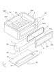
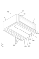
- FIG. 1 is a perspective view of an electronic component storage package according to an embodiment; 1 is an exploded perspective view of an electronic component storage package according to an embodiment of the present invention; 1 is a plan view of an electronic component storage package according to an embodiment of the present invention; 1 is a perspective view of an electronic component storage package according to an embodiment, as viewed from the bottom side. 1 is an exploded perspective view of an electronic component storage package according to an embodiment, as viewed from the bottom side; 6 is a cross-sectional view of the electronic component storage package shown in FIG. 3 taken along line VI-VI.
- FIG. 13 is a perspective view of an electronic component storage package according to another embodiment.
- FIG. 1 is an exploded perspective view of an electronic module according to an embodiment.
- the wiring board has a substrate body having laminated ceramic layers on which wiring layers of a predetermined pattern are formed and having a through hole, and a heat dissipation member inserted into the through hole.
- the substrate body may be damaged or deformed due to the difference in thermal expansion coefficient between the substrate body and the heat dissipation member, which may reduce the reliability of the wiring board.
- ⁇ Configuration of Electronic Component Storage Package> ⁇ Configuration of Electronic Component Storage Package>
- any direction of the electronic component storage package may be regarded as up or down, for convenience, a Cartesian coordinate system xyz is defined, and the positive side of the z direction is regarded as up.
- a plan view is a concept that includes a planar perspective view.
- an electronic component storage package 100 includes a substrate 1, a frame 2, and a base 3.
- the substrate 1 is a substrate having a frame body 2 and a base 3.
- the substrate 1 has a first upper surface 1u, a first lower surface 1b opposite to the first upper surface 1u, and a substrate through hole 1o.
- the substrate through hole 1o penetrates from the first upper surface 1u to the first lower surface 1b.
- the substrate 1 is, for example, rectangular in plan view, with dimensions of 1 mm x 2 mm to 25 mm x 50 mm, and a thickness (dimension in the z direction in the drawings) of 0.1 mm to 20 mm.
- the substrate 1 may also be rectangular with rounded or cut-out corners. This configuration can reduce the stress applied to the corners of the substrate 1.
- the substrate 1 is made of a first metal material.
- materials for the substrate 1 include metal materials such as copper, iron, tungsten, molybdenum, nickel, or cobalt, or alloys containing these metal materials.
- the substrate 1 may be a single metal plate or a laminate of multiple metal plates. If the substrate 1 is a single metal plate (in other words, made of one type of metal material), the substrate 1 can be easily processed. Furthermore, by reducing the thickness of the substrate 1, the electronic component storage package 100 can be made low-profile.
- the metal material constituting the substrate 1 is one of the above-mentioned metal materials, in order to reduce oxidation corrosion, a plating layer of nickel, gold, or the like may be formed on the surface of the substrate 1 by electroplating or electroless plating.
- the substrate 1 being made of a metal material here means that the substrate 1 is substantially made of a metal material, and may include, for example, a non-metallic material that is unavoidable in the manufacturing process. Since the substrate 1 is made of the first metal material, the substrate 1 can efficiently absorb heat generated from the electronic components 9 located on the base 3 (second upper surface 3u) described later, and dissipate the heat to the outside of the electronic component storage package 100.
- the substrate through hole 1o may have a square shape or a circular shape including an ellipse shape in a plan view.
- the substrate through hole 1o may have a rectangular shape having a long side in a direction in which a frame through hole 2o described later extends (the y direction in the drawings).
- the substrate through hole 1o may be rectangular with rounded corners, which can effectively reduce stress on the corners of the substrate through hole 1o.
- the substrate through-hole 1o can be formed by subjecting the substrate 1 to a known drilling process such as drilling, blasting, or laser processing.
- the frame 2 is located on the first upper surface 1u.
- the frame 2 surrounds the substrate through-hole 1o.
- the frame 2 is made of a ceramic material.
- the ceramic material referred to here includes, for example, an aluminum oxide sintered body, a mullite sintered body, a silicon carbide sintered body, an aluminum nitride sintered body, a silicon nitride sintered body, a glass ceramics, etc.
- the frame 2 being made of a ceramic material here means that it is substantially made of a ceramic material, and may include, for example, a metal material that is unavoidable in the manufacturing process. Since the frame body 2 is made of a ceramic material, it is easy to form wiring such as a wiring portion described below on the surface and inside of the frame body 2. Therefore, the electronic component storage package 100 can be made smaller.
- the frame body 2 is made of a metal material, it may be necessary to integrally mold the lid body 8 and the frame body 2, which will be described later, in order to improve the airtightness of the electronic module 10, which may increase the number of steps for integrally molding the lid body 8 and the frame body 2. Furthermore, large-scale equipment may be required to join the integrally molded lid body 8 and frame body 2 to the substrate 1. On the other hand, if the frame body 2 is made of a ceramic material, it is only necessary to position the lid body 8 on the frame body 2, which makes it easy to ensure the airtightness of the electronic module 10. Furthermore, the electronic module 10 can be easily manufactured.
- the frame body 2 has a frame body through hole 2o.
- the frame body through hole 2o penetrates the frame body 2 from the inside to the outside.
- “outside” refers to the direction away from the area surrounded by the frame body 2.
- “inside” refers to the direction approaching the area surrounded by the frame body 2, and refers to the opposite direction from “outside.”
- the frame body 2 may have a first wiring 201, a second wiring 202, and a third wiring 203, which will be described later, positioned therein. Also, via conductors and inner layer wiring may be positioned inside the frame body 2. Examples of materials for the first wiring 201 to the third wiring 203, the via conductors, and the inner layer wiring (hereinafter, these may be collectively referred to as the wiring portion) include metal materials such as gold, silver, copper, nickel, tungsten, molybdenum, and manganese.
- the wiring portion may be formed by sintering a metal paste at a predetermined position, or may be formed using a thin film formation technique such as a vapor deposition method or a sputtering method. Metal plating such as nickel plating or gold plating may be formed on the surface of the wiring portion. Also, an insulating film such as ceramic (e.g., an alumina coating) and/or resin may be located on a part of the wiring portion. The insulating film can be formed on the wiring portion by screen printing.
- An upper surface metal layer 204 may be located on at least a part of the upper surface of the frame 2. When the frame 2 has the upper surface metal layer 204, it becomes easy to bond a seal ring or a lid 8 onto the upper surface metal layer 204. Furthermore, a lower surface metal layer 205 may be located on at least a portion of the lower surface of the frame 2. Furthermore, the lower surface metal layer 205 may be located at a position overlapping with the substrate 1. This configuration makes it possible to easily bond the frame 2 and the substrate 1 to each other.
- the frame through-holes 2o may be formed by subjecting the frame 2 to known drilling processes such as drilling, blasting, and laser processing.
- the frame through-holes 2o may be formed by laminating ceramic green sheets that have been pre-formed into a shape with notches at the predetermined positions that will become the frame through-holes 2o.
- the pedestal 3 is located on the first upper surface 1u. As shown in FIG. 3, the pedestal 3 overlaps with the substrate through-hole 1o in a plan view.
- materials for the pedestal 3 include metal materials such as copper, iron, tungsten, molybdenum, nickel, and cobalt, or alloys containing these metal materials.
- the pedestal 3 may be a laminate in which multiple metal plates are stacked.
- a plating layer of nickel, gold, or the like may be formed on the surface of the pedestal 3 by electroplating or electroless plating in order to reduce oxidation corrosion.
- the base 3 may be made of a ceramic material such as an aluminum oxide sintered body, a mullite sintered body, a silicon carbide sintered body, an aluminum nitride sintered body, or a silicon nitride sintered body, or a dielectric material such as a glass ceramic material or a glass epoxy material.
- the base 3 may also be made of an organic resin material.
- the aforementioned substrate 1, frame 2, and base 3 may each be created by additive manufacturing (AM) using a 3D printer.
- AM additive manufacturing
- the first convex portion 33 protrudes from the second lower surface 3b. At least a portion of the first convex portion 33 is located within the substrate through hole 1o.
- An electronic component 9 (described later) is located on the upper surface of the base 3 (second upper surface 3u in the drawings), and the above configuration allows heat generated by the electronic component 9 to be efficiently dissipated to the outside. Furthermore, since the base 3 has the first convex portion 33, the first upper surface 1u and the second lower surface 3b, and the inner wall surface 11s and the convex portion side surface 33s can be joined and/or interlocked, increasing the opposing area between the base 3 and the substrate 1 and improving airtightness.
- the frame 2 when the heat from the electronic component 9 causes the base 3 and/or the substrate 1 to deform, the frame 2 also deforms, making it easier for cracks to occur around the frame through-hole 2o.
- the deformation of the base 3 and/or the substrate 1 can be reduced, reducing the possibility of cracks occurring around the frame through-hole 2o.
- the first protrusion 33 may be fitted into the substrate through hole 1o without using a bonding material, or may be indirectly fitted into the substrate through hole 1o via a first bonding material 61 described below.
- the first bonding material 61 may be located only between the first upper surface 1u and the second lower surface 3b, or may be located only between the inner wall surface 11s and the protrusion side surface 33s.
- the first convex portion 33 is positioned with a gap between all of the side surfaces of the base 3 (surfaces connecting the second upper surface 3u and the second lower surface 3b). Note that the convex portion side surface 33s of the first convex portion 33 described below may be flush with any of the side surfaces of the base 3. In other words, the base 3 only needs to have a stepped shape in a cross-sectional view.
- the base 3 may have multiple first convex portions 33.
- the first convex portion 33 may have a shape with a long side in the direction in which the frame through hole 2o extends (the y direction in the drawing) in a plan view.
- the electronic component 9 is a light-emitting element or a light-receiving element
- the electronic component 9 is arranged along the direction in which the frame through hole 2o extends, but with the above configuration, the first convex portion 33 is also arranged along the frame through hole 2o, so that heat generated by the electronic component 9 can be efficiently dissipated.
- the frame 2 may have a first side wall 21 and a second side wall 22.
- the second side wall 22 may face the first side wall 21 in the first direction.
- the first side wall 21 may have a frame through hole 2o.
- the distance L1 between the base 3 and the first side wall 21 in the first direction is smaller than the distance L2 between the base 3 and the second side wall 22 in the first direction.
- the base 3 is located close to the frame through hole 2o.
- the electronic component 9 is located on the second upper surface 3u, and if the electronic component 9 is a light-emitting element such as a semiconductor laser, the light emitted from the light-emitting element is emitted to the outside through the frame through hole 2o.
- the base 3 is located close to the frame through hole 2o, so that the light emitted from the light-emitting element can be efficiently emitted to the outside.
- the electronic component storage package 100 may further include a first bonding material 61 that bonds the base 3 and the substrate 1.
- the first convex portion 33 may have a convex lower surface 33b and a convex side surface 33s.
- the convex side surface 33s connects the convex lower surface 33b and the second lower surface 3b.
- the substrate through hole 1o has an inner wall surface 11s that faces the convex side surface 33s.
- the first bonding material 61 may be located between the first upper surface 1u and the second lower surface 3b and between the convex side surface 33s and the inner wall surface 11s.
- the material of the first bonding material 61 may be, for example, a resin material, a glass material, or a solder material. If the material of the first bonding material 61 is a silver solder material, the airtightness of the electronic component storage package 100 can be improved. Furthermore, if the material of the first bonding material 61 is a resin material, the bonding temperature between the frame body 2 and the base 3 can be lowered, thereby reducing the possibility of damage to the frame body 2 and the base 3 during bonding.
- the convex side surface 33s may be shaped to conform to the inner wall surface 11s of the substrate through hole 1o. This configuration can improve the airtightness of the electronic component storage package 100 while reducing the amount of first bonding material 61 used.
- the convex side surface 33s is perpendicular to the second lower surface 3b, but for example, the convex side surface 33s may have a tapered shape in which the width decreases from the first upper surface 1u toward the first lower surface 1b. This configuration makes it easier to fit the convex portion of the base 3 into the substrate through-hole 1o.
- Young's modulus E1 of substrate 1 may be greater than Young's modulus E2 of base 3. With this configuration, substrate 1 is less likely to deform than base 3, so that the possibility of electronic component storage package 100 being damaged when electronic component storage package 100 is subjected to an external impact can be reduced.
- the Young's modulus E1 of the substrate 1 may be smaller than the Young's modulus E3 of the frame body 2.
- the Young's modulus E3 of the frame body 2 may be greater than the Young's modulus E1 of the substrate 1 and greater than the Young's modulus E2 of the base 3.
- the Young's modulus E1 of the substrate 1 is between the Young's modulus E2 of the base 3 and the Young's modulus E3 of the frame body 2. Therefore, since the frame body 2 is less likely to deform than the substrate 1 and the base 3, the base 3 and the substrate 1 can be protected from external impacts. In addition, the possibility of the frame body 2 deforming and coming into contact with the base 3 can be reduced. In addition, since the frame body 2 is less likely to deform than the substrate 1, it is possible to reduce the possibility of the substrate 1 falling off the frame body 2 due to deformation of the frame body 2.
- the thermal expansion coefficient A3 of the frame 2 made of a ceramic material can be made closer to the thermal expansion coefficient A1 of the substrate 1, so that even if the substrate 1 thermally expands and deforms, the deformation due to thermal expansion of the frame 2 can follow the deformation of the substrate 1. Therefore, the possibility of the substrate 1 and the frame 2 becoming detached or damaged due to the difference in thermal expansion coefficients can be reduced.
- the first convex portion 33 may have a convex portion lower surface 33b.
- the convex portion lower surface 33b is located inward of the first imaginary surface.
- the convex portion lower surface 33b may be recessed with respect to the first lower surface 1b. More specifically, when the electronic component storage package 100 is viewed from below, a part of the inner wall surface 11s of the substrate through hole 1o may be exposed.
- the convex portion lower surface 33b refers to the surface facing the first imaginary plane.
- the frame body 2 may have a third lower surface 23b facing the first upper surface 1u.
- the third lower surface 23b may be exposed in a plan view seen from the first lower surface 1b side.
- the outer edge of the substrate 1 may be located inward from the outer edge of the frame body 2.
- the frame 2 may have a second wiring 202.
- the second wiring 202 is located on the third lower surface 23b.
- the second wiring 202 may be located with a gap between it and the substrate 1.
- the connection member 7 may be joined to the second wiring 202, and the inside and outside of the electronic component storage package 100 may be electrically connected.
- the second wiring 202 may be electrically connected to the first wiring 201 by a via conductor formed on the inner layer of the shelf portion 24.
- connection member 7 may be a lead terminal, but is not limited to this. That is, the connection member 7 may be, for example, a flexible printed circuit (FPC) or a printed circuit board (PCB) on which an electronic circuit is formed. In addition, a flexible circuit board or a printed circuit board on which an electronic circuit is formed may be connected to the end of the connection member 7.
- FPC flexible printed circuit
- PCB printed circuit board
- the electronic component storage package 100 may further include a light-transmitting member 4.
- the frame body 2 has an outer surface 211s.
- the light-transmitting member 4 may overlap the frame body through hole 2o and be located on the outer surface 211s.
- the translucent member 4 may be bonded to the outer surface 211s using a resin adhesive, a glass bonding material, or the like. In a side view, the translucent member 4 may overlap the entire frame through hole 2o, or may overlap only a portion of it. In one embodiment, the first side wall 21 may have the above-mentioned outer surface 211s.
- the light-transmitting member 4 may be a flat plate as shown in FIG. 2 or the like, a plate having a curved surface, or a sphere.
- the material of the light-transmitting member 4 may be resin or glass. More specifically, the material of the light-transmitting member 4 may be sapphire glass or borosilicate glass. Sapphire glass has superior strength and transmittance compared to borosilicate glass. Moreover, borosilicate glass is easier to process and manufacture compared to sapphire glass.
- the light-transmitting member 4 may have a structure in which transparent members are laminated in multiple layers. In one embodiment, the light-transmitting member 4 may be a lens. Furthermore, an optical fiber may be attached directly or indirectly to the light-transmitting member 4 .
- the thickness of the light-transmitting member 4 (here, the dimension in the x direction) is, for example, 0.1 mm to 1.0 mm.
- the translucent member 4 may have a first translucent surface 41s and a second translucent surface 42s.
- the first translucent surface 41s faces the outer surface 211s.
- the second translucent surface 42s is located on the opposite side to the first translucent surface 41s.
- a reflection reduction layer 43 may be located on at least a part of the surface of the light-transmitting member 4.
- the reflection reduction layer 43 may be, for example, an AR (Anti-Reflective) coat.
- the AR coat can be formed by vacuum deposition of, for example, magnesium fluoride.
- the thickness of the reflection reduction layer 43 is, for example, 50 nm to 500 nm. In this disclosure, for convenience, the description of the reflection reduction layer 43 is omitted in some drawings. More specifically, the reflection reduction layer 43 may be located on the first light-transmitting surface 41s and/or the second light-transmitting surface 42s. The reflection reduction layer 43 may be located at a distance from the outer edge of the light-transmitting member 4.
- a metallized layer may be located on at least a part of the surface of the light-transmitting member 4. This configuration can facilitate bonding between the annular member 5 described below and the light-transmitting member 4.
- the metallized layer may be formed in a position in contact with the annular member 5 described below.
- both the metallized layer and the reflection reduction layer 43 may be located on the surface of the light-transmitting member 4.
- the metallized layer may be located with a gap between it and the reflection reduction layer 43. More specifically, the metallized layer and the reflection reduction layer 43 may be located on the first light-transmitting surface 41s. In this case, the metallized layer may be in contact with the outer edge of the light-transmitting member 4 and may be located along the outer edge of the light-transmitting member 4.
- the reflection reduction layer 43 may be spaced apart from the metallized layer and may be surrounded by the metallized layer. This configuration reduces the possibility that the bonding strength between the light-transmitting member 4 and the frame 2, or the bonding strength between the light-transmitting member 4 and the annular member 5, will decrease due to the reflection reduction layer 43 covering the metallized layer.
- the electronic component storage package 100 may further include an annular member 5.
- the annular member 5 is located between the translucent member 4 and the outer surface 211s. With this configuration, the annular member 5 can absorb and cushion deformation caused by the difference between the thermal expansion coefficient of the frame body 2 and the thermal expansion coefficient of the translucent member 4. This reduces the possibility that the translucent member 4 will fall off the frame body 2.
- the material of the annular member 5 may be, for example, a metal material such as iron, copper, nickel, chromium, cobalt, molybdenum, or tungsten, or an alloy material that combines two or more of the above-mentioned metal materials, such as an iron-nickel alloy or an iron-cobalt-nickel alloy.
- the frame body 2 is made of a ceramic material, but even if the frame body 2 is made of a metal material, the annular member 5 can absorb and cushion deformation caused by the difference in thermal expansion coefficient between the frame body 2 made of a metal material and the translucent member 4.
- the material of the annular member 5 may be the same as or different from the material of the frame body 2.
- the annular member 5 may be molded integrally with the frame body 2.
- the area of the hole in the annular member 5 may be larger than the area of the frame through hole 2o and smaller than the area of the translucent member 4.
- the annular member 5 may be bonded to the metallized layer. This configuration makes it easier to bond the annular member 5 and the translucent member 4. In addition, the bonding strength between the annular member 5 and the translucent member 4 can be improved, thereby improving the airtightness of the electronic component storage package 100.
- the first side wall 21 may have a frame through hole 2o and a third wiring 203.
- the third wiring 203 may be positioned so as to overlap the frame through hole 2o.
- the third wiring 203 and the frame through hole 2o may be positioned on the same side wall (here, the first side wall 21) of the frame 2.
- the third wiring 203 may be positioned on the first side wall 21 side having the frame through hole 2o, rather than on the second side wall 22 side.
- the third wiring 203 and the frame through hole 2o on the same sidewall of the frame 2, other members (e.g., optical fibers and waveguides) connected to the light-transmitting member 4 can be positioned in the same direction as the connecting member 7 described below. Therefore, when the electronic component storage package 100 and the electronic module 10 are placed in, for example, a photoelectric conversion module, the area occupied by the electronic component storage package 100 and the electronic module 10 in the photoelectric conversion module can be reduced. Therefore, it is possible to effectively utilize the space in the photoelectric conversion module.
- other members e.g., optical fibers and waveguides
- the material of the third wiring 203 may be the same as that of the first wiring 201 and/or the second wiring 202, or may be a different material.
- the number of third wirings 203 may be one or more.
- the frame body 2 does not need to have the second wiring 202.
- the third wiring 203 may be electrically connected to the first wiring 201.
- the third wiring 203 and the first wiring 201 may be connected through an inner layer wiring or a via located inside the frame body 2.
- the third wirings 203 may be arranged on the first sidewall 21 along the longitudinal direction of the frame-body through-hole 2o (the y direction in the drawing).
- the third wiring 203 is located on the first side wall 21 (i.e., the upper surface of the frame body 2).
- the third wiring 203 only needs to be located so as to overlap the frame body through hole 2o in a plan view.
- the third wiring 203 may be located on the third lower surface 23b or on the side surface of the frame body 2 (in other words, the surface connecting the first side wall 21 and the second side wall 22).
- connection member 7 is a lead terminal, but is not limited to this.
- connection member 7 may be, for example, a flexible substrate or a printed circuit board on which an electronic circuit is formed.
- the electronic component storage package 100 may further include a second bonding material 62.
- the second bonding material 62 may be located between the translucent member 4 and the outer surface 211s.
- the material of the second bonding material 62 may be glass.
- the softening temperature of the second bonding material 62 may be lower than the softening temperature of the translucent member 4.
- the second bonding material 62 may be so-called low-melting glass.
- low-melting glass is amorphous or crystalline glass that softens, deforms, and flows at temperatures of 200°C to 600°C.
- Crystallizable glass means a composite of amorphous glass and crystalline glass.
- Low-melting glass borosilicate glass, barium borosilicate glass, zinc borate glass, barium borate glass, high silicic glass, aluminophosphate glass, phosphate glass, zinc phosphate glass, alkali glass, bismuth silicate glass, bismuth borosilicate glass, bismuth zinc borate glass, lead borosilicate glass, lead borate glass, potassium lead glass, crystalline lead glass, and the like can be applied.
- Low-melting glass has excellent airtightness compared to resin-based adhesives.
- Pb (lead)-free low melting point glass may be used. Pb-free means that the lead content is 0.1% by weight or less (RoHS (Restriction of the use of certain hazardous substances in electrical and electronic equipment) regulation).
- the second bonding material 62 may have a portion protruding from the second light-transmitting surface 42s in a plan view.
- the protruding portion of the second bonding material 62 can protect the light-transmitting member 4 from external obstacles. Therefore, the possibility that the light-transmitting member 4 falls off from the frame 2 can be reduced.
- the second bonding material 62 having a portion protruding from the second light-transmitting surface 42s means that the portion protrudes in the x direction in the drawings.
- the second bonding material 62 may have a ring shape that follows the edge of the translucent member 4.
- the ring shape reduces discontinuous portions of the second bonding material 62, making it possible to protect the translucent member 4 from external obstacles. This improves the strength and durability of the light-transmitting portion of the electronic component storage package 100. Furthermore, by making the second bonding material 62 continuous around the entire edge of the translucent member 4, the airtightness of the electronic component storage package 100 can be further improved.
- the area of the light-transmitting member 4 when viewed from the x direction, may be larger than the area of the frame body through hole 2o, and the area of the light-transmitting member 4 may be smaller than the area of the frame body through hole 2o. In this case, when viewed from the x direction, the entire light-transmitting member 4 may overlap with the frame body through hole 2o. This configuration reduces the possibility of direct contact between the light-transmitting member 4 and the frame body 2, thereby reducing the possibility of cracks occurring in the frame body through hole 2o and its surroundings due to thermal stress applied to the frame body 2.
- an electronic module 10 includes an electronic component storage package 100 , one or more electronic components 9 , and a lid 8 .
- the electronic component 9 is located on the base 3 (i.e., on the second upper surface 3u).
- the electronic component 9 may be directly mounted on the base 3, or may be indirectly mounted via a submount 91 as shown in FIG.
- the electronic component 9 may be electrically connected to the first wiring 201.
- the electronic component 9 and the first wiring 201 can be electrically connected by, for example, a bonding wire.
- the electronic component 9 may be, for example, an optical semiconductor element such as a semiconductor laser (LD) or a photodiode (PD), a semiconductor integrated circuit element, a sensor element such as an optical sensor, a power amplifier IC, etc.
- the electronic component 9 may be formed of a semiconductor material such as gallium arsenide or gallium nitride. More specifically, the electronic component 9 may be three light-emitting elements 9A to 9C, which may be elements that emit red (R), green (G), and blue (B) light, respectively.
- the electronic module 10 may be an RGB laser light source module, and may be used in information display devices such as VR goggles and AR glasses, for example.
- the lid 8 is located on the frame 2.
- the lid 8 protects the electronic components 9 together with the frame 2.
- Examples of materials for the lid 8 include metal materials, alloys made of multiple metal materials, and ceramics.
- the electronic module 10 may further include a seal ring located between the lid body 8 and the frame body 2.
- the seal ring is located on the frame body 2 and surrounds the electronic components 9 in a plan view. If no seal ring is provided on the frame body 2, the lid body 8 may be joined to the frame body 2 via an adhesive such as solder, brazing material, glass, or a resin adhesive.
- the electronic module 10 may have optical components such as a collimator lens, a Dylonic filter, a mirror, etc.
- the optical components may be located, for example, on the second upper surface 3u of the base 3, on the shelf portion 24, or on the substrate 1.
- This disclosure can be used as a package for storing electronic components and an electronic module using the same.
Landscapes
- Physics & Mathematics (AREA)
- Condensed Matter Physics & Semiconductors (AREA)
- General Physics & Mathematics (AREA)
- Electromagnetism (AREA)
- Optics & Photonics (AREA)
- Solid State Image Pick-Up Elements (AREA)
Priority Applications (1)
| Application Number | Priority Date | Filing Date | Title |
|---|---|---|---|
| JP2025522447A JPWO2024242165A1 (https=) | 2023-05-23 | 2024-05-23 |
Applications Claiming Priority (2)
| Application Number | Priority Date | Filing Date | Title |
|---|---|---|---|
| JP2023084723 | 2023-05-23 | ||
| JP2023-084723 | 2023-05-23 |
Publications (1)
| Publication Number | Publication Date |
|---|---|
| WO2024242165A1 true WO2024242165A1 (ja) | 2024-11-28 |
Family
ID=93589957
Family Applications (1)
| Application Number | Title | Priority Date | Filing Date |
|---|---|---|---|
| PCT/JP2024/018964 Ceased WO2024242165A1 (ja) | 2023-05-23 | 2024-05-23 | 電子部品収納用パッケージおよびこれを用いた電子モジュール |
Country Status (2)
| Country | Link |
|---|---|
| JP (1) | JPWO2024242165A1 (https=) |
| WO (1) | WO2024242165A1 (https=) |
Citations (3)
| Publication number | Priority date | Publication date | Assignee | Title |
|---|---|---|---|---|
| US20100097810A1 (en) * | 2008-10-16 | 2010-04-22 | Chia-Mao Li | Ultra high efficient encapsulation structure having metal heat sink |
| JP2012231101A (ja) * | 2011-04-25 | 2012-11-22 | Kostek Sys Co Ltd | メタルベース及びその製造方法並びにこれを用いた素子パッケージ |
| WO2014017273A1 (ja) * | 2012-07-27 | 2014-01-30 | 京セラ株式会社 | 半導体素子収納用パッケージおよび半導体装置 |
-
2024
- 2024-05-23 WO PCT/JP2024/018964 patent/WO2024242165A1/ja not_active Ceased
- 2024-05-23 JP JP2025522447A patent/JPWO2024242165A1/ja active Pending
Patent Citations (3)
| Publication number | Priority date | Publication date | Assignee | Title |
|---|---|---|---|---|
| US20100097810A1 (en) * | 2008-10-16 | 2010-04-22 | Chia-Mao Li | Ultra high efficient encapsulation structure having metal heat sink |
| JP2012231101A (ja) * | 2011-04-25 | 2012-11-22 | Kostek Sys Co Ltd | メタルベース及びその製造方法並びにこれを用いた素子パッケージ |
| WO2014017273A1 (ja) * | 2012-07-27 | 2014-01-30 | 京セラ株式会社 | 半導体素子収納用パッケージおよび半導体装置 |
Also Published As
| Publication number | Publication date |
|---|---|
| JPWO2024242165A1 (https=) | 2024-11-28 |
Similar Documents
| Publication | Publication Date | Title |
|---|---|---|
| US7037002B2 (en) | Optical component and method of manufacturing the same | |
| JP7238058B2 (ja) | 光導波路パッケージおよび発光装置 | |
| JP2006086176A (ja) | Led用サブマウント及びその製造方法 | |
| US12164175B2 (en) | Mounting package for an optical element with inclined transmission film and flat mirror | |
| JP6225834B2 (ja) | 半導体発光装置およびその製造方法 | |
| US7255494B2 (en) | Low-profile package for housing an optoelectronic assembly | |
| WO2024242165A1 (ja) | 電子部品収納用パッケージおよびこれを用いた電子モジュール | |
| JP4857709B2 (ja) | 発光装置 | |
| JP7703672B2 (ja) | 光導波路パッケージおよび発光装置 | |
| JP6485518B2 (ja) | 半導体発光装置およびその製造方法 | |
| JP4009110B2 (ja) | 光半導体素子収納用パッケージおよび光半導体装置 | |
| JP7685609B2 (ja) | 半導体パッケージおよび半導体装置 | |
| JP6092614B2 (ja) | 電子部品収納用パッケージおよびそれを用いた電子装置 | |
| TWI865917B (zh) | 光波導封裝及發光裝置 | |
| TWI864942B (zh) | 電子元件封裝體及其製造方法 | |
| WO2024204573A1 (ja) | 光学部品、光学部品を備えた光モジュール、および光学部品の製造方法 | |
| WO2003025652A1 (en) | Hermetically sealed package container for optical module | |
| US20250306319A1 (en) | Optical waveguide package and light-emitting device | |
| US20240329341A1 (en) | Light source module and xr glasses | |
| US11978998B2 (en) | Substrate for mounting a light-emitting element, array substrate, and light-emitting device | |
| WO2024225235A1 (ja) | 電子部品収納用パッケージおよび電子モジュール | |
| WO2024204657A1 (ja) | 光導波路パッケージ及び光源モジュール | |
| WO2024143486A1 (ja) | 光導波路パッケージおよび光源モジュール | |
| JP2017117899A (ja) | 電子部品収納用パッケージ | |
| JP2013206949A (ja) | 蓋体およびこれを用いた光半導体素子収納用パッケージ |
Legal Events
| Date | Code | Title | Description |
|---|---|---|---|
| 121 | Ep: the epo has been informed by wipo that ep was designated in this application |
Ref document number: 24811171 Country of ref document: EP Kind code of ref document: A1 |
|
| ENP | Entry into the national phase |
Ref document number: 2025522447 Country of ref document: JP Kind code of ref document: A |
|
| NENP | Non-entry into the national phase |
Ref country code: DE |