WO2024241912A1 - 電子部品 - Google Patents
電子部品 Download PDFInfo
- Publication number
- WO2024241912A1 WO2024241912A1 PCT/JP2024/017396 JP2024017396W WO2024241912A1 WO 2024241912 A1 WO2024241912 A1 WO 2024241912A1 JP 2024017396 W JP2024017396 W JP 2024017396W WO 2024241912 A1 WO2024241912 A1 WO 2024241912A1
- Authority
- WO
- WIPO (PCT)
- Prior art keywords
- coil
- bump electrode
- pattern
- exposed
- element body
- Prior art date
- Legal status (The legal status is an assumption and is not a legal conclusion. Google has not performed a legal analysis and makes no representation as to the accuracy of the status listed.)
- Ceased
Links
Images



Classifications
-
- H—ELECTRICITY
- H01—ELECTRIC ELEMENTS
- H01F—MAGNETS; INDUCTANCES; TRANSFORMERS; SELECTION OF MATERIALS FOR THEIR MAGNETIC PROPERTIES
- H01F17/00—Fixed inductances of the signal type
-
- H—ELECTRICITY
- H01—ELECTRIC ELEMENTS
- H01F—MAGNETS; INDUCTANCES; TRANSFORMERS; SELECTION OF MATERIALS FOR THEIR MAGNETIC PROPERTIES
- H01F17/00—Fixed inductances of the signal type
- H01F17/04—Fixed inductances of the signal type with magnetic core
-
- H—ELECTRICITY
- H01—ELECTRIC ELEMENTS
- H01F—MAGNETS; INDUCTANCES; TRANSFORMERS; SELECTION OF MATERIALS FOR THEIR MAGNETIC PROPERTIES
- H01F27/00—Details of transformers or inductances, in general
-
- H—ELECTRICITY
- H01—ELECTRIC ELEMENTS
- H01F—MAGNETS; INDUCTANCES; TRANSFORMERS; SELECTION OF MATERIALS FOR THEIR MAGNETIC PROPERTIES
- H01F27/00—Details of transformers or inductances, in general
- H01F27/28—Coils; Windings; Conductive connections
- H01F27/29—Terminals; Tapping arrangements for signal inductances
Definitions
- This disclosure relates to electronic components, and in particular to electronic components having a structure in which multiple coils are embedded in a base body containing a magnetic material.
- This disclosure describes a technology for improving the insulation between coils in an electronic component that has a structure in which multiple coils are embedded in a base body that contains a magnetic material.
- An electronic component has a mounting surface extending in a first direction and a second direction perpendicular or substantially perpendicular to the first direction, and includes a base body including a magnetic material, a first coil and a second coil embedded in the base body, the axial direction of which is a third direction perpendicular or substantially perpendicular to each of the first and second directions, and arranged in the first direction, a first bump electrode embedded in the base body, one end of which is connected to one end of the first coil and the other end of which is exposed on the mounting surface, and a second bump electrode embedded in the base body, one end of which is connected to the other end of the first coil and the other end of which is exposed on the mounting surface.
- a second bump electrode having one end connected to one end of the second coil and the other end exposed to the mounting surface; a third bump electrode having one end connected to the other end of the second coil and the other end exposed to the mounting surface; a first insulating resin layer is disposed between each of the first coil and the second coil and the magnetic material contained in the base body; and a second insulating resin layer is disposed between each of the first bump electrode, the second bump electrode, the third bump electrode, and the fourth bump electrode and the magnetic material contained in the base body.
- This disclosure provides a technology for improving the insulation between coils in an electronic component having a structure in which multiple coils are embedded in a base body containing a magnetic material.
- FIG. 1 is a schematic perspective view for explaining the structure of an electronic component (coil component) 100 according to an embodiment of the technology related to the present disclosure.
- FIG. 2 is an equivalent circuit diagram of the coil device 100.
- FIG. 3 is a schematic plan view showing the shape of the conductor pattern formed on the conductor layer L1.
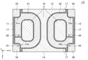
- FIG. 4 is a schematic plan view showing the shape of the conductor pattern formed on the conductor layer L2.
- FIG. 5 is a schematic plan view showing the shape of the conductor pattern formed on the conductor layer L3.
- FIG. 6 is a schematic plan view showing the shape of the conductor pattern formed on the conductor layer L4.
- the bump electrodes 21 and 23 are adjacent to each other in the X direction, and the bump electrodes 22 and 24 are adjacent to each other in the X direction.
- the bump electrode 21 may be exposed from the side surfaces 11 and 13 of the element body 10.
- the bump electrode 22 may be exposed from the side surfaces 11 and 14 of the element body 10.
- the bump electrode 23 may be exposed from the side surfaces 12 and 13 of the element body 10.
- the bump electrode 24 may be exposed from the side surfaces 12 and 14 of the element body 10.
- the base body 10 is embedded with multiple conductor layers L1 to L4 stacked in the Z direction, with coils C1 and C2 formed by conductor patterns located on conductor layers L1 to L3, and bump electrodes 21 to 24 formed by conductor patterns located on conductor layer L4.
- the axial directions of coils C1 and C2 are both in the Z direction.
- Coils C1 and C2 are also arranged in the longitudinal direction, the X direction.
- the surfaces of the conductor patterns located on conductor layers L1 to L4 are covered with an insulating resin layer to prevent direct contact with the base body 10, which is made of a magnetic material.
- the conductor patterns provided on the conductor layer L1 include coil patterns 31, 32 and dummy patterns 33, 34.
- the coil patterns 31, 32 are conductor patterns that rotate for approximately one turn, and one end of each is arranged at a position overlapping the bump electrodes 22, 24, respectively, in a plan view seen from the Z direction.
- the dummy patterns 33, 34 are arranged independently of the coil patterns 31, 32, and arranged at a position overlapping the bump electrodes 21, 23, respectively, in a plan view seen from the Z direction.
- One end and the other end of the coil pattern 31 are connected to the upper conductor layer L2 via via conductors 41, 42.
- One end and the other end of the coil pattern 32 are connected to the upper conductor layer L2 via via conductors 43, 44.
- connection patterns 55 and 56 are connected to one end of the coil patterns 31 and 32 via via conductors 41 and 43, respectively.
- An insulating resin layer 17 is provided between the coil patterns 51 and 52, the dummy patterns 53 and 54, and the connection patterns 55 and 56 and the element body 10, thereby preventing contact between them.
- the outer peripheral edge of the coil pattern 51 has notches 51a and 51b
- the outer peripheral edge of the coil pattern 52 has notches 52a and 52b.
- Parts of the dummy patterns 53 and 54 are arranged in the notches 51a and 52a so as to bite into the coil patterns 51 and 52, respectively.
- Parts of the connection patterns 55 and 56 are arranged in the notches 51b and 52b so as to bite into the coil patterns 51 and 52, respectively.
- a pattern is formed in which a part of the dummy pattern 53 enters (protrudes) into a part of the coil pattern 51 when viewed in a plan view from the Z direction.
- a pattern is formed in which a part of the dummy pattern 54 enters (protrudes) into a part of the coil pattern 52 when viewed in a plane from the Z direction.
- connection pattern 55 in the cutout 51b, a pattern is formed in which a part of the connection pattern 55 enters (protrudes) into a part of the coil pattern 51 when viewed in a plane from the Z direction.
- connection pattern 56 in the cutout 52b, a pattern is formed in which a part of the connection pattern 56 enters (protrudes) into a part of the coil pattern 52 when viewed in a plane from the Z direction.
- connection pattern 73 by disposing a portion of the connection pattern 73 within the notch 71a, a pattern is formed in which a portion of the connection pattern 73 enters (protrudes) into a portion of the coil pattern 71 when viewed in a plan view from the Z direction. Also, by disposing a portion of the connection pattern 74 within the notch 72a, a pattern is formed in which a portion of the connection pattern 74 enters (protrudes) into a portion of the coil pattern 72 when viewed in a plan view from the Z direction.
- the conductor pattern provided on the conductor layer L4 includes bump electrodes 21 to 24.
- the bump electrodes 21 to 24 are connected to the other end of the coil pattern 71, the connection pattern 73, the other end of the coil pattern 72, and the connection pattern 74 via via conductors 81 to 84, respectively.
- the bump electrode 21 overlaps with the dummy patterns 33 and 53 in a plan view seen from the Z direction, and has a larger area than the dummy patterns 33 and 53.
- the bump electrode 22 overlaps with the connection patterns 55 and 73 in a plan view seen from the Z direction, and has a larger area than the connection patterns 55 and 73.
- the bump electrode 23 overlaps with the dummy patterns 34 and 54 in a plan view seen from the Z direction, and has a larger area than the dummy patterns 34 and 54.
- the bump electrode 24 overlaps with the connection patterns 56, 74 in a plan view seen from the Z direction, and is larger in area than the connection patterns 56, 74.
- the distance between the bump electrodes 21 and 23, and the distance between the bump electrodes 22 and 24 can be made longer than the distance between the bump electrodes 21 and 22, and the distance between the bump electrodes 23 and 24. This makes it possible to further improve the insulation between the coils C1 and C2 on the mounting surface 15.
- the semiconductor device includes a second bump electrode having one end connected to one end of the second coil and the other end exposed to the mounting surface, a third bump electrode having one end connected to the other end of the second coil and the other end exposed to the mounting surface, and a fourth bump electrode having one end connected to the other end of the second coil and the other end exposed to the mounting surface.
- a first insulating resin layer is disposed between each of the first coil and the second coil and the magnetic material contained in the element body
- a second insulating resin layer is disposed between each of the first bump electrode, the second bump electrode, the third bump electrode, and the fourth bump electrode and the magnetic material contained in the element body.
- the base body further has a first side and a second side extending in the second direction and a third direction and positioned opposite each other, and a third side and a fourth side extending in the first direction and a third direction and positioned opposite each other, and the first bump electrode may be exposed on the first side and the third side, the second bump electrode may be exposed on the first side and the fourth side, the third bump electrode may be exposed on the second side and the third side, and the fourth bump electrode may be exposed on the second side and the fourth side.
- the second insulating resin layer may contain an inorganic filler. This reduces the thermal expansion coefficient of the second insulating resin layer, making it less likely for peeling to occur between components even if the thickness of the second insulating resin layer is increased.
- the turn has a portion overlapping the third bump electrode when viewed from the third direction
- the fourth pattern has a portion overlapping the fourth bump electrode when viewed from the third direction
- the area of the first bump electrode exposed on the mounting surface is larger than the area of the first pattern
- the area of the second bump electrode exposed on the mounting surface is larger than the area of the second pattern
- the area of the third bump electrode exposed on the mounting surface is larger than the area of the third pattern
- the area of the fourth bump electrode exposed on the mounting surface is larger than the area of the fourth pattern.
- the first conductor layer includes a first coil pattern constituting the first coil and a second coil pattern constituting the second coil, the outer peripheral edge of the first coil pattern has a first notch and a second notch, the outer peripheral edge of the second coil pattern has a third notch and a fourth notch, a part of the first pattern is arranged in the first notch so as to cut into the first coil pattern, a part of the second pattern is arranged in the second notch so as to cut into the first coil pattern, a part of the third pattern is arranged in the third notch so as to cut into the second coil pattern, and a part of the fourth pattern is arranged in the fourth notch so as to cut into the second coil pattern.
Landscapes
- Engineering & Computer Science (AREA)
- Power Engineering (AREA)
- Microelectronics & Electronic Packaging (AREA)
- Coils Or Transformers For Communication (AREA)
Priority Applications (2)
| Application Number | Priority Date | Filing Date | Title |
|---|---|---|---|
| CN202480034575.7A CN121368811A (zh) | 2023-05-25 | 2024-05-10 | 电子部件 |
| JP2025522303A JPWO2024241912A1 (https=) | 2023-05-25 | 2024-05-10 |
Applications Claiming Priority (2)
| Application Number | Priority Date | Filing Date | Title |
|---|---|---|---|
| JP2023086321 | 2023-05-25 | ||
| JP2023-086321 | 2023-05-25 |
Publications (1)
| Publication Number | Publication Date |
|---|---|
| WO2024241912A1 true WO2024241912A1 (ja) | 2024-11-28 |
Family
ID=93589189
Family Applications (1)
| Application Number | Title | Priority Date | Filing Date |
|---|---|---|---|
| PCT/JP2024/017396 Ceased WO2024241912A1 (ja) | 2023-05-25 | 2024-05-10 | 電子部品 |
Country Status (3)
| Country | Link |
|---|---|
| JP (1) | JPWO2024241912A1 (https=) |
| CN (1) | CN121368811A (https=) |
| WO (1) | WO2024241912A1 (https=) |
Citations (5)
| Publication number | Priority date | Publication date | Assignee | Title |
|---|---|---|---|---|
| JP2014107435A (ja) * | 2012-11-28 | 2014-06-09 | Tdk Corp | コモンモードフィルタ |
| JP2014116589A (ja) * | 2012-12-11 | 2014-06-26 | Samsung Electro-Mechanics Co Ltd | 電子部品及び電子部品の製造方法 |
| JP2020155479A (ja) * | 2019-03-18 | 2020-09-24 | Tdk株式会社 | コイル部品及びその製造方法 |
| JP2021052076A (ja) * | 2019-09-25 | 2021-04-01 | Tdk株式会社 | コイル部品及びその製造方法 |
| JP2021068825A (ja) * | 2019-10-24 | 2021-04-30 | 株式会社村田製作所 | インダクタアレイ部品およびインダクタアレイ部品内蔵基板 |
-
2024
- 2024-05-10 CN CN202480034575.7A patent/CN121368811A/zh active Pending
- 2024-05-10 WO PCT/JP2024/017396 patent/WO2024241912A1/ja not_active Ceased
- 2024-05-10 JP JP2025522303A patent/JPWO2024241912A1/ja active Pending
Patent Citations (5)
| Publication number | Priority date | Publication date | Assignee | Title |
|---|---|---|---|---|
| JP2014107435A (ja) * | 2012-11-28 | 2014-06-09 | Tdk Corp | コモンモードフィルタ |
| JP2014116589A (ja) * | 2012-12-11 | 2014-06-26 | Samsung Electro-Mechanics Co Ltd | 電子部品及び電子部品の製造方法 |
| JP2020155479A (ja) * | 2019-03-18 | 2020-09-24 | Tdk株式会社 | コイル部品及びその製造方法 |
| JP2021052076A (ja) * | 2019-09-25 | 2021-04-01 | Tdk株式会社 | コイル部品及びその製造方法 |
| JP2021068825A (ja) * | 2019-10-24 | 2021-04-30 | 株式会社村田製作所 | インダクタアレイ部品およびインダクタアレイ部品内蔵基板 |
Also Published As
| Publication number | Publication date |
|---|---|
| CN121368811A (zh) | 2026-01-20 |
| JPWO2024241912A1 (https=) | 2024-11-28 |
Similar Documents
| Publication | Publication Date | Title |
|---|---|---|
| US9196415B2 (en) | Coil component | |
| JP7452507B2 (ja) | インダクタ | |
| US20230317358A1 (en) | Coil component | |
| JPH11238634A (ja) | 面実装型コイル部品 | |
| US10347416B2 (en) | Coil component, circuit board provided with the same, and manufacturing method for coil component | |
| CN116052974A (zh) | 线圈零件 | |
| JP7449660B2 (ja) | インダクタ部品 | |
| WO2024241912A1 (ja) | 電子部品 | |
| US11742134B2 (en) | Coil component and circuit board having the same | |
| JP2023047358A (ja) | インダクタ | |
| JP2023148787A (ja) | コイル部品 | |
| US20250125077A1 (en) | Coil component | |
| JP2024154856A (ja) | 電子部品 | |
| WO2024219267A1 (ja) | 電子部品 | |
| WO2024070406A1 (ja) | コイル部品 | |
| WO2025069662A1 (ja) | 電子部品 | |
| US20260081058A1 (en) | Coil component | |
| JPH0810176Y2 (ja) | プリント基板組込形チョークコイル | |
| US20250104898A1 (en) | Coil component | |
| TWI864560B (zh) | 平面變壓器 | |
| US20260011487A1 (en) | Electronic component | |
| WO2025197462A1 (ja) | 電子部品 | |
| US20240290529A1 (en) | Coil component | |
| JP2023106738A (ja) | コイル部品 | |
| WO2025164569A1 (ja) | 電子部品及びこれを備える部品内蔵基板 |
Legal Events
| Date | Code | Title | Description |
|---|---|---|---|
| 121 | Ep: the epo has been informed by wipo that ep was designated in this application |
Ref document number: 24810920 Country of ref document: EP Kind code of ref document: A1 |
|
| WWE | Wipo information: entry into national phase |
Ref document number: 2025522303 Country of ref document: JP |
|
| NENP | Non-entry into the national phase |
Ref country code: DE |