WO2024241786A1 - 接合構造、半導体装置、および接合方法 - Google Patents
接合構造、半導体装置、および接合方法 Download PDFInfo
- Publication number
- WO2024241786A1 WO2024241786A1 PCT/JP2024/015532 JP2024015532W WO2024241786A1 WO 2024241786 A1 WO2024241786 A1 WO 2024241786A1 JP 2024015532 W JP2024015532 W JP 2024015532W WO 2024241786 A1 WO2024241786 A1 WO 2024241786A1
- Authority
- WO
- WIPO (PCT)
- Prior art keywords
- conductive
- layer
- metal
- semiconductor device
- terminal
- Prior art date
- Legal status (The legal status is an assumption and is not a legal conclusion. Google has not performed a legal analysis and makes no representation as to the accuracy of the status listed.)
- Ceased
Links
Images









Classifications
-
- H—ELECTRICITY
- H10—SEMICONDUCTOR DEVICES; ELECTRIC SOLID-STATE DEVICES NOT OTHERWISE PROVIDED FOR
- H10W—GENERIC PACKAGES, INTERCONNECTIONS, CONNECTORS OR OTHER CONSTRUCTIONAL DETAILS OF DEVICES COVERED BY CLASS H10
- H10W72/00—Interconnections or connectors in packages
- H10W72/30—Die-attach connectors
-
- H—ELECTRICITY
- H10—SEMICONDUCTOR DEVICES; ELECTRIC SOLID-STATE DEVICES NOT OTHERWISE PROVIDED FOR
- H10W—GENERIC PACKAGES, INTERCONNECTIONS, CONNECTORS OR OTHER CONSTRUCTIONAL DETAILS OF DEVICES COVERED BY CLASS H10
- H10W40/00—Arrangements for thermal protection or thermal control
- H10W40/60—Securing means for detachable heating or cooling arrangements, e.g. clamps
-
- H—ELECTRICITY
- H10—SEMICONDUCTOR DEVICES; ELECTRIC SOLID-STATE DEVICES NOT OTHERWISE PROVIDED FOR
- H10W—GENERIC PACKAGES, INTERCONNECTIONS, CONNECTORS OR OTHER CONSTRUCTIONAL DETAILS OF DEVICES COVERED BY CLASS H10
- H10W70/00—Package substrates; Interposers; Redistribution layers [RDL]
- H10W70/60—Insulating or insulated package substrates; Interposers; Redistribution layers
-
- H—ELECTRICITY
- H10—SEMICONDUCTOR DEVICES; ELECTRIC SOLID-STATE DEVICES NOT OTHERWISE PROVIDED FOR
- H10W—GENERIC PACKAGES, INTERCONNECTIONS, CONNECTORS OR OTHER CONSTRUCTIONAL DETAILS OF DEVICES COVERED BY CLASS H10
- H10W72/00—Interconnections or connectors in packages
- H10W72/071—Connecting or disconnecting
-
- H—ELECTRICITY
- H10—SEMICONDUCTOR DEVICES; ELECTRIC SOLID-STATE DEVICES NOT OTHERWISE PROVIDED FOR
- H10W—GENERIC PACKAGES, INTERCONNECTIONS, CONNECTORS OR OTHER CONSTRUCTIONAL DETAILS OF DEVICES COVERED BY CLASS H10
- H10W72/00—Interconnections or connectors in packages
- H10W72/071—Connecting or disconnecting
- H10W72/073—Connecting or disconnecting of die-attach connectors
-
- H—ELECTRICITY
- H10—SEMICONDUCTOR DEVICES; ELECTRIC SOLID-STATE DEVICES NOT OTHERWISE PROVIDED FOR
- H10W—GENERIC PACKAGES, INTERCONNECTIONS, CONNECTORS OR OTHER CONSTRUCTIONAL DETAILS OF DEVICES COVERED BY CLASS H10
- H10W74/00—Encapsulations, e.g. protective coatings
- H10W74/40—Encapsulations, e.g. protective coatings characterised by their materials
-
- H—ELECTRICITY
- H10—SEMICONDUCTOR DEVICES; ELECTRIC SOLID-STATE DEVICES NOT OTHERWISE PROVIDED FOR
- H10W—GENERIC PACKAGES, INTERCONNECTIONS, CONNECTORS OR OTHER CONSTRUCTIONAL DETAILS OF DEVICES COVERED BY CLASS H10
- H10W90/00—Package configurations
-
- H—ELECTRICITY
- H10—SEMICONDUCTOR DEVICES; ELECTRIC SOLID-STATE DEVICES NOT OTHERWISE PROVIDED FOR
- H10W—GENERIC PACKAGES, INTERCONNECTIONS, CONNECTORS OR OTHER CONSTRUCTIONAL DETAILS OF DEVICES COVERED BY CLASS H10
- H10W99/00—Subject matter not provided for in other groups of this subclass
-
- H—ELECTRICITY
- H10—SEMICONDUCTOR DEVICES; ELECTRIC SOLID-STATE DEVICES NOT OTHERWISE PROVIDED FOR
- H10W—GENERIC PACKAGES, INTERCONNECTIONS, CONNECTORS OR OTHER CONSTRUCTIONAL DETAILS OF DEVICES COVERED BY CLASS H10
- H10W72/00—Interconnections or connectors in packages
- H10W72/071—Connecting or disconnecting
- H10W72/073—Connecting or disconnecting of die-attach connectors
- H10W72/07331—Connecting techniques
-
- H—ELECTRICITY
- H10—SEMICONDUCTOR DEVICES; ELECTRIC SOLID-STATE DEVICES NOT OTHERWISE PROVIDED FOR
- H10W—GENERIC PACKAGES, INTERCONNECTIONS, CONNECTORS OR OTHER CONSTRUCTIONAL DETAILS OF DEVICES COVERED BY CLASS H10
- H10W72/00—Interconnections or connectors in packages
- H10W72/30—Die-attach connectors
- H10W72/351—Materials of die-attach connectors
- H10W72/352—Materials of die-attach connectors comprising metals or metalloids, e.g. solders
-
- H—ELECTRICITY
- H10—SEMICONDUCTOR DEVICES; ELECTRIC SOLID-STATE DEVICES NOT OTHERWISE PROVIDED FOR
- H10W—GENERIC PACKAGES, INTERCONNECTIONS, CONNECTORS OR OTHER CONSTRUCTIONAL DETAILS OF DEVICES COVERED BY CLASS H10
- H10W72/00—Interconnections or connectors in packages
- H10W72/90—Bond pads, in general
- H10W72/951—Materials of bond pads
- H10W72/952—Materials of bond pads comprising metals or metalloids, e.g. PbSn, Ag or Cu
-
- H—ELECTRICITY
- H10—SEMICONDUCTOR DEVICES; ELECTRIC SOLID-STATE DEVICES NOT OTHERWISE PROVIDED FOR
- H10W—GENERIC PACKAGES, INTERCONNECTIONS, CONNECTORS OR OTHER CONSTRUCTIONAL DETAILS OF DEVICES COVERED BY CLASS H10
- H10W90/00—Package configurations
- H10W90/701—Package configurations characterised by the relative positions of pads or connectors relative to package parts
- H10W90/731—Package configurations characterised by the relative positions of pads or connectors relative to package parts of die-attach connectors
- H10W90/734—Package configurations characterised by the relative positions of pads or connectors relative to package parts of die-attach connectors between a chip and a stacked insulating package substrate, interposer or RDL
Definitions
- This disclosure relates to a joining structure, a semiconductor device, and a joining method.
- Patent Document 1 discloses an example of a conventional semiconductor device.
- the semiconductor device disclosed in this document comprises a semiconductor element, a conductive member, a support member, and a sealing resin.
- the semiconductor element is bonded to the main surface of the conductive member.
- a second metal layer containing Ag (silver) is disposed on the back surface of the conductive member.
- a first metal layer containing Ag (silver) is disposed on the support surface of the support member.
- the conductive member and support member are bonded by solid-state diffusion bonding of the first metal layer and the second metal layer.
- the present disclosure has an objective to provide an improved joining method, a joining structure using the joining method, and a semiconductor device including the joining structure.
- the present disclosure has an objective to provide a joining method that can simplify the joining process and reduce costs when solid-state joining a first member and a second member, a joining structure using the joining method, and a semiconductor device including the joining structure.
- the joining structure provided by the first aspect of the present disclosure comprises a first member having a first layer mainly composed of a first metal, and a second member having a second layer mainly composed of a second metal different from the first metal, and the first layer of the first member and the second layer of the second member are solid-state joined.
- the semiconductor device provided by the second aspect of the present disclosure includes the junction structure provided by the first aspect and a semiconductor element.
- the joining method provided by the third aspect of the present disclosure includes the steps of preparing a first member having a first layer mainly composed of a first metal and a second member having a second layer mainly composed of a second metal different from the first metal, and solid-state joining the first layer of the first member and the second layer of the second member.
- the above configuration for example, in terms of the joining method, can simplify the joining process and reduce costs.
- FIG. 1 is a perspective view showing a semiconductor device according to a first embodiment of the present disclosure.
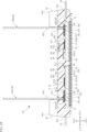
- FIG. 2 is a perspective view of FIG. 1 with the sealing resin omitted.
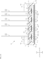
- FIG. 3 is a perspective view of FIG. 2 with the first conductive member omitted.
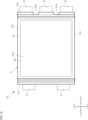
- FIG. 4 is a plan view showing the semiconductor device according to the first embodiment of the present disclosure.
- FIG. 5 is a plan view of FIG. 4 in which the sealing resin is shown by imaginary lines.
- FIG. 6 is a partially enlarged view of a part of FIG. 5, with the sealing resin omitted.
- FIG. 7 is a plan view of FIG. 5 in which the sealing resin and the first conductive member are omitted and the second conductive member is shown by imaginary lines.
- FIG. 1 is a perspective view showing a semiconductor device according to a first embodiment of the present disclosure.
- FIG. 2 is a perspective view of FIG. 1 with the sealing resin omitted.
- FIG. 3 is a perspective view of FIG. 2 with the first
- FIG. 8 is a bottom view showing the semiconductor device according to the first embodiment of the present disclosure.
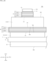
- FIG. 9 is a cross-sectional view taken along line IX-IX in FIG.
- FIG. 10 is a cross-sectional view taken along line XX in FIG.
- FIG. 11 is a partially enlarged view of a part of FIG.
- FIG. 12 is a partially enlarged view of a part of FIG.
- FIG. 13 is a cross-sectional view taken along line XIII-XIII in FIG.
- FIG. 14 is a cross-sectional view taken along line XIV-XIV in FIG.
- FIG. 15 is a cross-sectional view taken along line XV-XV in FIG.
- FIG. 10 is a cross-sectional view taken along line XX in FIG.
- FIG. 11 is a partially enlarged view of a part of FIG.
- FIG. 12 is a partially enlarged view of a part of FIG.
- FIG. 13 is a cross-sectional view
- FIG. 16 is a schematic diagram for explaining the joint structure of the semiconductor device according to the first embodiment of the present disclosure, and is a schematic diagram of a front view in which the sealing resin and the like are omitted.
- FIG. 17 is an image of the bonded portion between the bonding member and the support substrate taken with a scanning electron microscope.
- FIG. 18 is a schematic front view showing a step of an example of a method for manufacturing a semiconductor device according to the first embodiment of the present disclosure.
- FIG. 19 is a cross-sectional view showing an example of a semiconductor device assembly including the semiconductor device according to the first embodiment of the present disclosure.
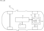
- FIG. 20 is a schematic diagram of a vehicle equipped with the semiconductor device according to the first embodiment of the present disclosure.
- FIG. 21 is a cross-sectional view showing a semiconductor device according to the second embodiment of the present disclosure.
- FIG. 22 is a schematic front view for explaining a joining structure of a semiconductor device according to a second embodiment of the present disclosure.
- an object A is formed on an object B" and “an object A is formed on an object B” include “an object A is formed directly on an object B” and “an object A is formed on an object B with another object interposed between the object A and the object B” unless otherwise specified.
- an object A is disposed on an object B” and “an object A is disposed on an object B” include “an object A is disposed directly on an object B” and “an object A is disposed on an object B with another object interposed between the object A and the object B" unless otherwise specified.
- an object A is located on an object B includes “an object A is located on an object B in contact with an object B” and “an object A is located on an object B with another object interposed between the object A and the object B” unless otherwise specified.
- an object A overlaps an object B when viewed in a certain direction includes “an object A overlaps the entire object B” and “an object A overlaps a part of an object B.”
- a surface A faces in direction B is not limited to the case where the angle of surface A with respect to direction B is 90°, but also includes the case where surface A is tilted with respect to direction B.
- First embodiment: 1 to 16 show a semiconductor device according to a first embodiment of the present disclosure.
- the semiconductor device A1 of this embodiment includes a plurality of first semiconductor elements 10A, a plurality of second semiconductor elements 10B, a conductive substrate 2, a support substrate 3, bonding members 19, 29, a first terminal 41, a second terminal 42, a plurality of third terminals 43, a fourth terminal 44, a plurality of control terminals 45, a control terminal support body 48, a first conductive member 5, a second conductive member 6, and a sealing resin 8.
- FIG. 1 is a perspective view showing the semiconductor device A1.
- FIG. 2 is a perspective view of FIG. 1 with the sealing resin 8 omitted.
- FIG. 3 is a perspective view of FIG. 2 with the first conductive member 5 omitted.
- FIG. 4 is a plan view showing the semiconductor device A1.
- FIG. 5 is a plan view of FIG. 4 with the sealing resin 8 shown in phantom lines.
- FIG. 6 is a partial enlarged view of FIG. 5 with the sealing resin 8 omitted.
- FIG. 7 is a plan view of FIG. 5 with the sealing resin 8 and the first conductive member 5 omitted and the second conductive member 6 shown in phantom lines.
- FIG. 8 is a bottom view of the semiconductor device A1.
- FIG. 8 is a bottom view of the semiconductor device A1.
- FIG. 9 is a cross-sectional view taken along line IX-IX in FIG. 5.
- FIG. 10 is a cross-sectional view taken along line X-X in FIG. 5.
- FIG. 11 and FIG. 12 are partial enlarged views of FIG. 10.
- FIG. 13 is a cross-sectional view taken along line XIII-XIII in FIG. 5.
- 14 is a cross-sectional view taken along line XIV-XIV in FIG. 5.
- FIG. 15 is a cross-sectional view taken along line XV-XV in FIG. 5.
- FIG. 16 is a schematic diagram for explaining the bonding structure of the semiconductor device shown in FIGS. 1 to 15, and is a schematic diagram of a front view with the sealing resin 8 and the like omitted.
- the thickness direction of the semiconductor device A1 is referred to as the "thickness direction z.”
- One direction perpendicular to the thickness direction z is referred to as the "first direction x.”
- a direction perpendicular to both the thickness direction z and the first direction x is referred to as the "second direction y.”
- planar view refers to a view in the thickness direction z.
- the z1 side of the thickness direction z may be referred to as the top, and the z2 side of the thickness direction z may be referred to as the bottom.
- Each of the first semiconductor elements 10A and the second semiconductor elements 10B is an electronic component that is the core of the function of the semiconductor device A1, and is an example of a "semiconductor element" of the present disclosure.
- the constituent material of each of the first semiconductor elements 10A and the second semiconductor elements 10B is a semiconductor material mainly made of, for example, SiC (silicon carbide). This semiconductor material is not limited to SiC, and may be Si (silicon), GaN (gallium nitride), or C (diamond), etc.
- Each of the first semiconductor elements 10A and the second semiconductor elements 10B is, for example, a power semiconductor chip having a switching function such as a MOSFET (Metal Oxide Semiconductor Field Effect Transistor).
- MOSFET Metal Oxide Semiconductor Field Effect Transistor
- the first semiconductor element 10A and the second semiconductor element 10B are shown as MOSFETs, but are not limited thereto, and may be other transistors such as an IGBT (Insulated Gate Bipolar Transistor).
- IGBT Insulated Gate Bipolar Transistor
- Each of the first semiconductor elements 10A and each of the second semiconductor elements 10B are the same element.
- Each of the first semiconductor elements 10A and each of the second semiconductor elements 10B is, for example, an n-channel MOSFET, but may also be a p-channel MOSFET.
- the first semiconductor element 10A and the second semiconductor element 10B each have an element main surface 101 and an element back surface 102.
- the element main surface 101 and the element back surface 102 are separated in the thickness direction z.
- the element main surface 101 faces the z1 side in the thickness direction z
- the element back surface 102 faces the z2 side in the thickness direction z.
- the semiconductor device A1 has four first semiconductor elements 10A and four second semiconductor elements 10B, but the number of first semiconductor elements 10A and the number of second semiconductor elements 10B are not limited to this configuration and are changed as appropriate according to the performance required of the semiconductor device A1.
- four first semiconductor elements 10A and four second semiconductor elements 10B are arranged.
- the number of first semiconductor elements 10A and the number of second semiconductor elements 10B may be two or three, or five or more.
- the number of first semiconductor elements 10A and the number of second semiconductor elements 10B may be equal to or different from each other.
- the number of first semiconductor elements 10A and the number of second semiconductor elements 10B are determined by the current capacity handled by the semiconductor device A1.
- the semiconductor device A1 is configured, for example, as a half-bridge type switching circuit.
- the multiple second semiconductor elements 10B configure the upper arm circuit of the semiconductor device A1
- the multiple first semiconductor elements 10A configure the lower arm circuit.
- the multiple second semiconductor elements 10B are connected in parallel to each other, and in the lower arm circuit, the multiple first semiconductor elements 10A are connected in parallel to each other.
- Each second semiconductor element 10B and each first semiconductor element 10A are connected in series to configure a bridge layer.
- the multiple first semiconductor elements 10A are mounted on the conductive substrate 2, as shown in Figures 7 and 14. In the example shown in Figure 7, the multiple first semiconductor elements 10A are lined up, for example, in the second direction y and spaced apart from one another. Each first semiconductor element 10A is conductively joined to the conductive substrate 2 (first conductive portion 2A described below) via a joining member 19. When each first semiconductor element 10A is joined to the first conductive portion 2A, the element back surface 102 faces the first conductive portion 2A.
- the multiple second semiconductor elements 10B are mounted on the conductive substrate 2 as shown in FIG. 7, FIG. 15, etc.
- the multiple second semiconductor elements 10B are arranged, for example, in the second direction y and are spaced apart from one another.
- Each second semiconductor element 10B is conductively joined to the conductive substrate 2 (second conductive portion 2B described below) via a joining member 19.
- the element back surface 102 faces the second conductive portion 2B.
- the multiple first semiconductor elements 10A and the multiple second semiconductor elements 10B overlap when viewed in the first direction x, but they do not have to overlap.
- the multiple first semiconductor elements 10A and the multiple second semiconductor elements 10B each have a first principal surface electrode 11, a second principal surface electrode 12, a third principal surface electrode 13, and a back surface electrode 15.
- the configurations of the first principal surface electrode 11, the second principal surface electrode 12, the third principal surface electrode 13, and the back surface electrode 15 described below are common to each of the first semiconductor elements 10A and each of the second semiconductor elements 10B.
- the first principal surface electrode 11, the second principal surface electrode 12, and the third principal surface electrode 13 are provided on the element principal surface 101.
- the first principal surface electrode 11, the second principal surface electrode 12, and the third principal surface electrode 13 are insulated by an insulating film (not shown).
- the back surface electrode 15 is provided on the element back surface 102.
- the first principal surface electrode 11 is, for example, a gate electrode, to which a drive signal (for example, a gate voltage) for driving the first semiconductor element 10A (second semiconductor element 10B) is input.
- the second principal surface electrode 12 is, for example, a source electrode through which a source current flows.
- the third principal surface electrode 13 is, for example, a source sense electrode through which a source current flows.
- the back surface electrode 15 is, for example, a drain electrode through which a drain current flows.
- the back surface electrode 15 covers the entire area (or substantially the entire area) of the element back surface 102.
- the back surface electrode 15 is formed by Ag (silver) sputtering.
- the back surface electrode 15 may be formed by Au (gold) sputtering.
- each first semiconductor element 10A switches between a conductive state and a cut-off state in response to the drive signal.
- a current flows from the back surface electrode 15 (drain electrode) to the second principal surface electrode 12 (source electrode), and in the cut-off state, this current does not flow.
- Each first semiconductor element 10A (each second semiconductor element 10B) performs a switching operation.
- the semiconductor device A1 converts a DC voltage input between the one fourth terminal 44 and the two first terminals 41 and second terminals 42 into, for example, an AC voltage by the switching function of the multiple first semiconductor elements 10A and multiple second semiconductor elements 10B, and outputs the AC voltage from the third terminal 43.
- the semiconductor device A1 includes a thermistor 17.
- the thermistor 17 is used as a temperature detection sensor.
- the conductive substrate 2 supports a plurality of first semiconductor elements 10A and a plurality of second semiconductor elements 10B.
- the conductive substrate 2 is conductively joined to the support substrate 3 via a joining member 29.
- the constituent material of the conductive substrate 2 is, for example, mainly composed of Cu (copper). "Mainly composed" includes cases where nothing other than the main component is included. In other words, the constituent material of the conductive substrate 2 may be Cu containing no other components, or may be a Cu alloy.
- the constituent material of the conductive substrate 2 is not limited, and may be mainly composed of another metal.
- the conductive substrate 2 includes a first conductive portion 2A and a second conductive portion 2B.
- the first conductive portion 2A and the second conductive portion 2B are each a plate-like member having a rectangular shape in a plan view.
- the first conductive portion 2A and the second conductive portion 2B, together with the first terminal 41, the second terminal 42, the plurality of third terminals 43, the fourth terminal 44, the first conductive member 5, and the second conductive member 6, constitute a conduction path of a main circuit current to the plurality of first semiconductor elements 10A and the plurality of second semiconductor elements 10B.
- the first conductive portion 2A and the second conductive portion 2B are each conductively joined to the support substrate 3 via a bonding member 29.
- the first conductive portion 2A is conductively joined to the plurality of first semiconductor elements 10A via a bonding member 19.
- the second conductive portion 2B is conductively joined to the plurality of second semiconductor elements 10B via a bonding member 19.
- the first conductive portion 2A and the second conductive portion 2B are spaced apart in the first direction x, as shown in FIGS. 3, 7, 9, and 10.
- the first conductive portion 2A is located on the x1 side in the first direction x relative to the second conductive portion 2B.
- the first conductive portion 2A and the second conductive portion 2B overlap when viewed in the first direction x.
- the first conductive portion 2A and the second conductive portion 2B each have a dimension in the first direction x of, for example, 15 mm to 25 mm, a dimension in the second direction y of, for example, 30 mm to 40 mm, and a dimension in the thickness direction z of, for example, 1.0 mm to 5.0 mm (preferably about 2.0 mm).
- the conductive substrate 2 has a main surface 201 and a back surface 202.
- the main surface 201 and the back surface 202 are spaced apart in the thickness direction z, as shown in Figures 9, 10, 13 to 15, and 16.
- the main surface 201 faces the z1 side in the thickness direction z
- the back surface 202 faces the z2 side in the thickness direction z.
- the main surface 201 is a combination of the upper surface of the first conductive portion 2A and the upper surface of the second conductive portion 2B.
- a plurality of first semiconductor elements 10A and a plurality of second semiconductor elements 10B are conductively bonded to the main surface 201 via a bonding member 19.
- the back surface 202 is a combination of the lower surface of the first conductive portion 2A and the lower surface of the second conductive portion 2B.
- the back surface 202 is conductively bonded to the support substrate 3 via a bonding member 29 so as to face the support substrate 3.
- No metal layer such as Ag (silver) plating is disposed on the main surface 201 and the back surface 202 of the conductive substrate 2.
- the supporting substrate 3 supports the conductive substrate 2.
- the supporting substrate 3 is, for example, an AMB (Active Metal Brazing) substrate.
- the supporting substrate 3 includes an insulating layer 31, a first metal layer 32, and a second metal layer 33.
- the insulating layer 31 is, for example, a ceramic with excellent thermal conductivity.
- An example of such a ceramic is SiN (silicon nitride).
- the insulating layer 31 is not limited to ceramics, and may be an insulating resin sheet or the like.
- the insulating layer 31 is, for example, rectangular in plan view.
- the second metal layer 33 is formed on the upper surface (surface facing the z1 side in the thickness direction z) of the insulating layer 31.
- the constituent material of the second metal layer 33 is, for example, mainly composed of Cu (copper), and may be Cu or a Cu alloy.
- the constituent material of the second metal layer 33 is not limited, and may be mainly composed of other metals such as Al (aluminum).
- the second metal layer 33 includes a first portion 33A and a second portion 33B.
- the first portion 33A and the second portion 33B are spaced apart in the first direction x.
- the first portion 33A is located on the x1 side of the second portion 33B in the first direction x.
- the first portion 33A is conductively joined to the first conductive portion 2A via the joining member 29, and supports the first conductive portion 2A.
- the second portion 33B is conductively joined to the second conductive portion 2B via the joining member 29, and supports the second conductive portion 2B.
- the first portion 33A and the second portion 33B are each, for example, rectangular in plan view.
- the first metal layer 32 is formed on the lower surface of the insulating layer 31 (the surface facing the z2 side in the thickness direction z).
- the constituent material of the first metal layer 32 is the same as the constituent material of the second metal layer 33.
- the lower surface of the first metal layer 32 (the bottom surface 302 described below) is exposed from the sealing resin 8, as shown in FIG. 8. In a plan view, the first metal layer 32 overlaps both the first portion 33A and the second portion 33B.
- the support substrate 3 has a support surface 301 and a bottom surface 302.
- the support surface 301 and the bottom surface 302 are spaced apart in the thickness direction z.
- the support surface 301 faces the z1 side in the thickness direction z
- the bottom surface 302 faces the z2 side in the thickness direction z.
- the bottom surface 302 is exposed from the sealing resin 8 as shown in Figure 8.
- the second metal layer 33 has the support surface 301
- the first metal layer 32 has the bottom surface 302.
- the support surface 301 is the upper surface of the second metal layer 33, and is formed by combining the upper surface of the first portion 33A and the upper surface of the second portion 33B.
- the support surface 301 faces the conductive substrate 2, and the conductive substrate 2 is conductively joined via the joining member 29.
- the bottom surface 302 is the lower surface of the first metal layer 32.
- a heat dissipation member such as a heat sink (not shown) can be attached to the bottom surface 302.
- No metal layer such as Ag (silver) plating is disposed on the support surface 301 and bottom surface 302 of the support substrate 3.
- the dimension of the support substrate 3 in the thickness direction z (the distance from the support surface 301 to the bottom surface 302 along the thickness direction z) is, for example, 0.7 mm to 2.0 mm.
- the bonding member 19 is interposed between the first semiconductor element 10A (second semiconductor element 10B) and the first conductive portion 2A (second conductive portion 2B) of the conductive substrate 2, and electrically connects the first semiconductor element 10A (second semiconductor element 10B) and the first conductive portion 2A (second conductive portion 2B).
- the bonding member 19 and the first semiconductor element 10A (second semiconductor element 10B) are solid-state bonded, and the bonding member 19 and the first conductive portion 2A (second conductive portion 2B) are solid-state bonded.
- the bonding member 29 is interposed between the first conductive portion 2A (second conductive portion 2B) of the conductive substrate 2 and the first portion 33A (second portion 33B) of the second metal layer 33 of the support substrate 3, and electrically connects the first conductive portion 2A (second conductive portion 2B) and the first portion 33A (second portion 33B).
- the joining member 29 and the first conductive portion 2A (second conductive portion 2B) are solid-state welded, and the joining member 29 and the first portion 33A (second portion 33B) are solid-state welded.
- the joining member 19 and the joining member 29 are metal foils with a thickness dimension (dimension in the thickness direction z) of about 100 ⁇ m.
- the joining members 19 and 29 include a main body layer 191, a surface layer 192, a back layer 193, and intermediate layers 194 and 195.
- the main body layer 191 is the main body of the joining members 19 and 29, and is made of, for example, Al (aluminum) or an Al alloy.
- the intermediate layer 194 is disposed in contact with the surface of the main body layer 191 facing the z1 side in the thickness direction z.
- the intermediate layer 194 includes a Ni layer 194a in contact with the main body layer 191, and a Cu layer 194b in contact with the Ni layer 194a.
- the surface layer 192 is disposed in contact with the surface of the intermediate layer 194 facing the z1 side in the thickness direction z, and is located closest to the z1 side of the joining members 19 and 29.
- the surface layer 192 is made of Ag.
- the intermediate layer 195 is disposed in contact with the surface of the main body layer 191 facing the z2 side in the thickness direction z.
- the intermediate layer 195 includes a Ni layer 195a in contact with the main body layer 191, and a Cu layer 195b in contact with the Ni layer 195a.
- the back surface layer 193 is disposed in contact with a surface of the intermediate layer 195 facing the z2 side in the thickness direction z, and is located closest to the z2 side of the bonding members 19, 29.
- the constituent material of the back surface layer 193 is Ag. That is, the surface layer 192 and the back surface layer 193 made of Ag are disposed on both ends of the bonding members 19, 29 in the thickness direction z.
- the intermediate layers 194, 195 are formed by, for example, plating the main body layer 191.
- the surface layer 192 is formed by, for example, plating the intermediate layer 194.
- the back surface layer 193 is formed by, for example, plating the intermediate layer 195.
- the method of forming the bonding members 19, 29 is not limited.
- the constituent materials of the main body layer 191, the surface layer 192, the back surface layer 193, and the intermediate layers 194, 195 are not limited.
- the constituent material of the surface layer 192 and the back layer 193 may be an alloy containing Ag, or may be primarily composed of Au.
- the bonding member 19 has a principal surface 19a and a rear surface 19b.
- the principal surface 19a and the rear surface 19b are spaced apart in the thickness direction z as shown in FIG. 16.
- the principal surface 19a faces the z1 side in the thickness direction z
- the rear surface 19b faces the z2 side in the thickness direction z.
- the principal surface 19a faces the z1 side in the thickness direction z of the front layer 192, and faces the first semiconductor element 10A (second semiconductor element 10B).
- the rear surface 19b faces the z2 side in the thickness direction z of the rear surface layer 193, and faces the conductive substrate 2.
- the bonding member 29 has a principal surface 29a and a rear surface 29b.
- the principal surface 29a and the rear surface 29b are spaced apart in the thickness direction z as shown in FIG. 16.
- the principal surface 29a faces the z1 side in the thickness direction z
- the rear surface 29b faces the z2 side in the thickness direction z.
- the main surface 29a faces the z1 side of the thickness direction z of the surface layer 192 and faces the conductive substrate 2.
- the back surface 29b faces the z2 side of the thickness direction z of the back surface layer 193 and faces the support substrate 3.
- the surface layer 192 (principal surface 19a) of the joining member 19 is solid-state bonded to the back electrode 15 of the first semiconductor element 10A (second semiconductor element 10B).
- the back layer 193 (back surface 19b) of the joining member 19 is solid-state bonded to the main surface 201 of the first conductive portion 2A (second conductive portion 2B) of the conductive substrate 2.
- the surface layer 192 (principal surface 29a) of the joining member 29 is solid-state bonded to the back surface 202 of the first conductive portion 2A (second conductive portion 2B) of the conductive substrate 2.
- the back layer 193 (back surface 29b) of the joining member 29 is solid-state bonded to the second metal layer 33 (support surface 301) of the support substrate 3.
- the support substrate 3, bonding member 29, conductive substrate 2, bonding member 19, and first semiconductor element 10A (second semiconductor element 10B) are placed in this order in the thickness direction z and transported to a pressure device that performs solid-state bonding, and solid-state bonding is performed between each component in a single pressure treatment.
- Figure 17 is an image of the bonded portion between the bonding member 29 and the support substrate 3 taken with a scanning electron microscope (SEM). The image shows the state after 100 cycles of a temperature cycle test. As shown in Figure 17, the bonded interface between the back surface layer 193 (back surface 29b) of the bonding member 29 and the second metal layer 33 (support surface 301) of the support substrate 3 is in an appropriately bonded state.
- SEM scanning electron microscope
- the first terminal 41, the second terminal 42, the multiple third terminals 43, and the fourth terminal 44 are each made of a plate-shaped metal plate.
- the metal plate is made of, for example, Cu or a Cu alloy.
- the semiconductor device A1 has one each of the first terminal 41, the second terminal 42, and the fourth terminal 44, and two third terminals 43.
- the DC voltage to be converted is input to the first terminal 41, the second terminal 42, and the fourth terminal 44.
- the fourth terminal 44 is a positive electrode (P terminal), and the first terminal 41 and the second terminal 42 are negative electrodes (N terminals).
- the AC voltage converted by the first semiconductor element 10A and the second semiconductor element 10B is output from the multiple third terminals 43.
- the first terminal 41, the second terminal 42, the multiple third terminals 43, and the fourth terminal 44 each include a portion covered by the sealing resin 8 and a portion exposed from the sealing resin 8.
- the fourth terminal 44 is formed integrally with the second conductive portion 2B as shown in FIG. 10. Unlike this configuration, the fourth terminal 44 may be separated from the second conductive portion 2B and conductively joined to the second conductive portion 2B. As shown in FIG. 7 and other figures, the fourth terminal 44 is located on the x2 side of the first direction x with respect to the second semiconductor elements 10B and the second conductive portion 2B (conductive substrate 2). The fourth terminal 44 is conductive to the second conductive portion 2B and is conductive to the back electrode 15 (drain electrode) of each second semiconductor element 10B via the second conductive portion 2B.
- the first terminal 41 and the second terminal 42 are each spaced apart from the second conductive portion 2B, as shown in FIG. 7.
- the first terminal 41 and the second terminal 42 are each joined to a first conductive member 5, as shown in FIG. 5 and FIG. 6.
- the first terminal 41 and the second terminal 42 are each located on the x2 side of the first direction x with respect to the second semiconductor elements 10B and the second conductive portion 2B (conductive substrate 2), as shown in FIG. 5, FIG. 7, etc.
- the first terminal 41 and the second terminal 42 are each electrically connected to the first conductive member 5, and are also electrically connected to the second principal surface electrode 12 (source electrode) of each first semiconductor element 10A via the first conductive member 5.
- the first terminal 41, the second terminal 42, and the fourth terminal 44 each protrude from the sealing resin 8 to the x2 side in the first direction x in the semiconductor device A1.
- the first terminal 41, the second terminal 42, and the fourth terminal 44 are spaced apart from each other.
- the first terminal 41 and the second terminal 42 are located on opposite sides of the fourth terminal 44 in the second direction y.
- the first terminal 41 is located on the y2 side of the fourth terminal 44 in the second direction y
- the second terminal 42 is located on the y1 side of the fourth terminal 44 in the second direction y.
- the first terminal 41, the second terminal 42, and the fourth terminal 44 overlap each other when viewed in the second direction y.
- each of the two third terminals 43 is formed integrally with the first conductive portion 2A. Unlike the present configuration, the third terminal 43 may be separated from the first conductive portion 2A and conductively joined to the first conductive portion 2A. As shown in Fig. 7 and other figures, each of the two third terminals 43 is connected to the plurality of first semiconductor elements 10A and the first conductive portion 2A (conductive substrate 2). 4A, and is located on the x1 side in the first direction x. Each third terminal 43 is electrically connected to the first conductive portion 2A, and is also electrically connected to the back electrode 15 (drain electrode) of each first semiconductor element 10A via the first conductive portion 2A.
- the number of third terminals 43 is not limited to two, and may be, for example, one, or three or more. For example, when there is one third terminal 43, it is desirable that it is connected to the center portion in the second direction y of the first conductive portion 2A.
- the multiple control terminals 45 are pin-shaped terminals for controlling each of the first semiconductor elements 10A and each of the second semiconductor elements 10B.
- the multiple control terminals 45 include multiple first control terminals 46A-46D and multiple second control terminals 47A-47E.
- the multiple first control terminals 46A-46D are used to control each of the first semiconductor elements 10A, etc.
- the multiple second control terminals 47A-47E are used to control each of the second semiconductor elements 10B, etc.
- the multiple first control terminals 46A-46D are arranged at intervals in the second direction y. As shown in Figures 7 and 10, each of the first control terminals 46A-46D is supported by the first conductive portion 2A via a control terminal support 48 (first support portion 48A described below). As shown in Figures 5 and 7, each of the first control terminals 46A-46D is located between the multiple first semiconductor elements 10A and the two third terminals 43 in the first direction x.
- the first control terminal 46A is a terminal (gate terminal) for inputting a drive signal to the multiple first semiconductor elements 10A.
- a drive signal for driving the multiple first semiconductor elements 10A is input to the first control terminal 46A (for example, a gate voltage is applied).
- the first control terminal 46B is a terminal (source sense terminal) for detecting source signals of the multiple first semiconductor elements 10A.
- the first control terminal 46B detects the voltage (voltage corresponding to the source current) applied to each second principal surface electrode 12 (source electrode) of the multiple first semiconductor elements 10A.
- the first control terminal 46C and the first control terminal 46D are terminals that are electrically connected to thermistor 17.
- the second control terminals 47A-47E are spaced apart in the second direction y. As shown in Figures 7 and 10, each of the second control terminals 47A-47E is supported by the second conductive portion 2B via a control terminal support 48 (second support portion 48B, described below). As shown in Figures 5 and 7, each of the second control terminals 47A-47E is located between the second semiconductor elements 10B and the first terminal 41, second terminal 42, and fourth terminal 44 in the first direction x.
- the second control terminal 47A is a terminal (gate terminal) for inputting a drive signal for the multiple second semiconductor elements 10B.
- a drive signal for driving the multiple second semiconductor elements 10B is input to the second control terminal 47A (for example, a gate voltage is applied).
- the second control terminal 47B is a terminal (source sense terminal) for detecting source signals of the multiple second semiconductor elements 10B.
- the second control terminal 47B detects a voltage (voltage corresponding to a source current) applied to each second principal surface electrode 12 (source electrode) of the multiple second semiconductor elements 10B.
- the second control terminal 47C and the second control terminal 47D are terminals that are conductive to the thermistor 17.
- the second control terminal 47E is a terminal (drain sense terminal) for detecting drain signals of the multiple second semiconductor elements 10B.
- the second control terminal 47E detects a voltage (voltage corresponding to a drain current) applied to each back surface electrode 15 (drain electrode) of the multiple second semiconductor elements 10B.
- Each of the multiple control terminals 45 includes a holder 451 and a metal pin 452.
- the holder 451 is made of a conductive material. As shown in FIG. 11 and FIG. 12, the holder 451 is bonded to the control terminal support 48 (first metal layer 482 described later) via a conductive bonding material 459.
- the material of the conductive bonding material 459 is not particularly limited, and may be, for example, solder, a metal paste material, or a sintered metal.
- the holder 451 includes a cylindrical portion, an upper end flange, and a lower end flange. The upper end flange is connected to the upper part of the cylindrical portion, and the lower end flange is connected to the lower part of the cylindrical portion.
- a metal pin 452 is inserted into at least the upper end flange and the cylindrical portion of the holder 451. Most of the holder 451 is covered with the sealing resin 8. In the illustrated example, only the upper end surface of each holder 451 is exposed from the sealing resin 8.
- the metal pin 452 is a rod-shaped member extending in the thickness direction z.
- the metal pin 452 is supported by being pressed into the holder 451.
- the metal pin 452 is electrically connected to the control terminal support 48 (first metal layer 482 described below) at least via the holder 451.
- the control terminal support 48 first metal layer 482 described below
- the metal pin 452 is electrically connected to the control terminal support 48 via the conductive bonding material 459.
- the length of the metal pin 452 in the thickness direction z is not limited to the example shown in the figure and can be selected as appropriate.
- the control terminal support 48 supports the multiple control terminals 45.
- the control terminal support 48 is interposed between the main surface 201 (conductive substrate 2) and the multiple control terminals 45 in the thickness direction z.
- the control terminal support 48 includes a first support portion 48A and a second support portion 48B.
- the first support portion 48A is disposed on the first conductive portion 2A of the conductive substrate 2, and supports the first control terminals 46A to 46D of the control terminals 45.
- the first support portion 48A is bonded to the first conductive portion 2A via a bonding material 49, as shown in FIG. 11.
- the bonding material 49 may be conductive or insulating, and may be, for example, solder.
- the second support portion 48B is disposed on the second conductive portion 2B of the conductive substrate 2, and supports the second control terminals 47A to 47E of the control terminals 45.
- the second support portion 48B is bonded to the second conductive portion 2B via a bonding material 49, as shown in FIG. 12.
- the control terminal support 48 (each of the first support portion 48A and the second support portion 48B) is formed, for example, from a DBC (Direct Bonded Copper) substrate.
- the control terminal support 48 has an insulating layer 481, a first metal layer 482, and a second metal layer 483 stacked on top of each other.
- the insulating layer 481 is made of, for example, ceramics.
- the insulating layer 481 is, for example, rectangular in plan view.
- the first metal layer 482 is formed on the upper surface of the insulating layer 481, as shown in Figures 11 and 12. Each control terminal 45 is provided upright on the first metal layer 482.
- the first metal layer 482 is, for example, Cu or a Cu alloy.
- the first metal layer 482 includes a first portion 482A, a second portion 482B, a third portion 482C, a fourth portion 482D, a fifth portion 482E, and a sixth portion 482F.
- the first portion 482A, the second portion 482B, the third portion 482C, the fourth portion 482D, the fifth portion 482E, and the sixth portion 482F are separated and insulated from each other.
- the first portion 482A has a plurality of wires 71 bonded thereto, and is electrically connected to the first principal surface electrodes 11 (gate electrodes) of the first semiconductor elements 10A (second semiconductor elements 10B) via the respective wires 71.
- the first portion 482A and the sixth portion 482F are connected to a plurality of wires 73.
- the sixth portion 482F is electrically connected to the first principal surface electrodes 11 (gate electrodes) of the first semiconductor elements 10A (second semiconductor elements 10B) via the wires 73 and 71.
- the first control terminal 46A is bonded to the sixth portion 482F of the first support 48A
- the second control terminal 47A is bonded to the sixth portion 482F of the second support 48B.
- the second portion 482B has a plurality of wires 72 bonded thereto, and is electrically connected to the second principal surface electrode 12 (source electrode) of each of the first semiconductor elements 10A (each of the second semiconductor elements 10B) via each of the wires 72.
- the first control terminal 46B is bonded to the second portion 482B of the first support portion 48A
- the second control terminal 47B is bonded to the second portion 482B of the second support portion 48B.
- the thermistor 17 is joined to the third portion 482C and the fourth portion 482D. As shown in FIG. 7, the first control terminals 46C and 46D are joined to the third portion 482C and the fourth portion 482D of the first support portion 48A, and the second control terminals 47C and 47D are joined to the third portion 482C and the fourth portion 482D of the second support portion 48B.
- the fifth portion 482E of the first support portion 48A is not electrically connected to the other components.
- a wire 74 is joined to the fifth portion 482E of the second support portion 48B, and is electrically connected to the second conductive portion 2B via the wire 74.
- a second control terminal 47E is joined to the fifth portion 482E of the second support portion 48B.
- Each of the wires 71 to 74 is, for example, a bonding wire.
- the material of each of the wires 71 to 74 is not particularly limited, and may include, for example, any of Au (gold), Al, or Cu.
- the second metal layer 483 is formed on the lower surface of the insulating layer 481, as shown in Figures 11 and 12.
- the second metal layer 483 is, for example, Cu or a Cu alloy.
- the second metal layer 483 of the first support portion 48A is bonded to the first conductive portion 2A via a bonding material 49, as shown in Figure 11.
- the second metal layer 483 of the second support portion 48B is bonded to the second conductive portion 2B via a bonding material 49, as shown in Figure 12.
- the first conductive member 5 and the second conductive member 6 are spaced apart from the main surface 201 (conductive substrate 2) on the z1 side in the thickness direction z, and overlap the main surface 201 in a plan view.
- the first conductive member 5 and the second conductive member 6 are each made of a metal plate material.
- the metal is, for example, Cu or a Cu alloy.
- the first conductive member 5 and the second conductive member 6 are metal plate materials that are appropriately bent.
- the first conductive member 5 is connected to the second main surface electrode 12 (source electrode) of each first semiconductor element 10A and the first terminal 41 and second terminal 42, and electrically connects the second main surface electrode 12 of each first semiconductor element 10A to the first terminal 41 and second terminal 42.
- the first conductive member 5 forms a path for a main circuit current that is switched by the multiple first semiconductor elements 10A.
- the first conductive member 5 has a maximum dimension in the first direction x of, for example, 25 mm to 40 mm, and a maximum dimension in the second direction y of, for example, 30 mm to 45 mm.
- the first conductive member 5 includes a first wiring portion 51, a second wiring portion 52, a third wiring portion 53, a fourth wiring portion 54, and a fifth wiring portion 55.
- the first wiring portion 51 has a first end 511, a second end 512, and a plurality of openings 513.
- the first end 511 is connected to the first terminal 41.
- the first end 511 and the first terminal 41 are joined by a conductive bonding material 59.
- the material of the conductive bonding material 59 is not particularly limited, and may be, for example, solder, a metal paste material, or a sintered metal.
- the first wiring portion 51 is a band-shaped portion extending overall in the first direction x in a plan view.
- the first wiring portion 51 overlaps with both the second conductive portion 2B and the first conductive portion 2A in a plan view.
- the second end 512 is spaced apart from the first end 511 in the first direction x. As shown in FIG. 6, the second end 512 is located on the x1 side of the first direction x from the first end 511.
- Each of the multiple openings 513 is a partially cut out portion in a plan view.
- the multiple openings 513 are spaced apart from one another in the first direction x.
- the first wiring portion 51 has three openings 513.
- the opening 513 on the x2 side of the first direction x and the central opening 513 in the first direction x are located in a position that overlaps the main surface 201 of the second conductive portion 2B (conductive substrate 2) in a plan view, and does not overlap the multiple second semiconductor elements 10B in a plan view.
- the opening 513 on the x1 side of the first direction x is located in a position that overlaps the main surface 201 of the first conductive portion 2A (conductive substrate 2) in a plan view, and does not overlap the multiple first semiconductor elements 10A in a plan view.
- Each opening 513 is provided toward the y2 side of the second conductive portion 2B (first conductive portion 2A) in the second direction y in a plan view.
- the opening 513 is an arc-shaped notch recessed from the end on the y1 side in the second direction y to the y2 side in the second direction y in the first wiring part 51.
- the planar shape of the opening 513 is not limited, and may be a notch as in this embodiment, or may be a hole as in this embodiment.
- the second wiring portion 52 has a third end 521, a fourth end 522, and a plurality of openings 523.
- the third end 521 is connected to the second terminal 42.
- the third end 521 and the second terminal 42 are joined by a conductive bonding material 59.
- the second wiring portion 52 is a band-shaped portion extending in the first direction x as a whole in a planar view.
- the second wiring portion 52 is disposed away from the first wiring portion 51 in the second direction y.
- the second wiring portion 52 is located on the y1 side of the first wiring portion 51 in the second direction y.
- the second wiring portion 52 overlaps with both the second conductive portion 2B and the first conductive portion 2A in a planar view.
- the fourth end 522 is spaced apart from the third end 521 in the first direction x. As shown in FIG. 6, the fourth end 522 is located on the x1 side in the first direction x from the third end 521.
- Each of the multiple openings 523 is a partially cut out portion in a plan view.
- the multiple openings 523 are spaced apart from one another in the first direction x.
- the second wiring portion 52 has three openings 523.
- the opening 523 on the x2 side of the first direction x and the central opening 523 in the first direction x are located in a position that overlaps the main surface 201 of the second conductive portion 2B (conductive substrate 2) in a plan view, and does not overlap the multiple second semiconductor elements 10B in a plan view.
- the opening 523 on the x1 side of the first direction x is located in a position that overlaps the main surface 201 of the first conductive portion 2A (conductive substrate 2) in a plan view, and does not overlap the multiple first semiconductor elements 10A in a plan view.
- Each opening 523 is provided toward the y1 side of the second conductive portion 2B (first conductive portion 2A) in the second direction y in a plan view.
- the opening 523 is an arc-shaped notch recessed from the end on the y2 side in the second direction y to the y1 side in the second direction y in the second wiring part 52.
- the planar shape of the opening 523 is not limited, and may be a notch as in this embodiment, or may be a hole as in this embodiment.
- the third wiring portion 53 is connected to both the first wiring portion 51 (second end 512) and the second wiring portion 52 (fourth end 522).
- the third wiring portion 53 is a band-shaped portion extending in the second direction y in a planar view. As can be seen from FIG. 6 and other figures, the third wiring portion 53 overlaps multiple first semiconductor elements 10A in a planar view.
- the third wiring portion 53 is connected to each first semiconductor element 10A as shown in FIG. 14.
- the third wiring part 53 has a plurality of recessed regions 531. As shown in FIG. 14 and the like, each recessed region 531 has a shape that protrudes toward the z2 side in the thickness direction z more than other parts of the third wiring part 53. Each of the plurality of recessed regions 531 is bonded to one of the plurality of first semiconductor elements 10A. Each recessed region 531 of the third wiring part 53 and the second main surface electrode 12 of each first semiconductor element 10A are bonded via a conductive bonding material 59. In this embodiment, an opening 531a is formed in each recessed region 531. Each opening 531a is preferably formed so as to overlap the center of the first semiconductor element 10A in a plan view.
- the opening 531a is, for example, a through hole formed in each recessed region 531 of the third wiring part 53.
- the opening 531a is used, for example, when positioning the first conductive member 5 with respect to the conductive substrate 2.
- the planar shape of the opening 531a may be a perfect circle, or may be another shape such as an ellipse or a rectangle.
- the fourth wiring portion 54 is connected to both the first wiring portion 51 and the second wiring portion 52.
- the fourth wiring portion 54 is a band-shaped portion extending in the second direction y in a plan view.
- the fourth wiring portion 54 is connected to the first wiring portion 51 between the first end 511 and the second end 512, and is connected to the second wiring portion 52 between the third end 521 and the fourth end 522.
- the fourth wiring portion 54 is separated from the third wiring portion 53 in the first direction x. As shown in FIG. 6 and other figures, the fourth wiring portion 54 is located on the x2 side of the first direction x with respect to the third wiring portion 53.
- the fourth wiring portion 54 overlaps a plurality of second semiconductor elements 10B in a plan view.
- the fourth wiring portion 54 has a plurality of convex regions 541. As shown in FIG. 15 and other figures, each convex region 541 protrudes further toward the z1 side in the thickness direction z than other portions of the fourth wiring portion 54. As shown in FIG. 6, FIG. 15 and other figures, the plurality of convex regions 541 and the plurality of second semiconductor elements 10B overlap each other in a planar view. In this embodiment, as can be seen from FIG. 6 and other figures, the plurality of concave regions 531 in the third wiring portion 53 and the plurality of convex regions 541 are positioned equal to each other in the second direction y.
- the fifth wiring portion 55 is connected to both the third wiring portion 53 and the fourth wiring portion 54.
- the fifth wiring portion 55 is a band-shaped portion extending in the first direction x in a plan view.
- the first conductive member 5 includes a plurality (three) of fifth wiring portions 55.
- the plurality of fifth wiring portions 55 are located between the first wiring portion 51 and the second wiring portion 52 in the second direction y, and are arranged at intervals in the second direction y.
- the plurality of fifth wiring portions 55 are arranged in parallel (or approximately parallel).
- the end of each of the plurality of fifth wiring portions 55 on the x1 side in the first direction x is connected between two recessed regions 531 of the third wiring portion 53 adjacent to each other in the second direction y.
- the end of each of the plurality of fifth wiring portions 55 on the x2 side in the first direction x is connected between two convex regions 541 of the fourth wiring portion 54 adjacent to each other in the second direction y.
- the second conductive member 6 is connected to the second principal surface electrode 12 (source electrode) and the first conductive portion 2A of each second semiconductor element 10B, and provides electrical continuity between the second principal surface electrode 12 and the first conductive portion 2A of each second semiconductor element 10B.
- the second conductive member 6 forms a path for the main circuit current that is switched by the multiple second semiconductor elements 10B.
- the second conductive member 6 includes a main portion 61, multiple first connection ends 62, and multiple second connection ends 63.
- the main portion 61 is located between the second semiconductor elements 10B and the first conductive portion 2A in the first direction x, and is a band-shaped portion extending in the second direction y in a planar view. As shown in FIG. 13, the main portion 61 is located on the z2 side in the thickness direction z with respect to the fifth wiring portion 55 of the first conductive member 5, and is located closer to the main surface 201 (conductive substrate 2) than the fifth wiring portion 55. The main portion 61 overlaps the fifth wiring portions 55 in a planar view. In this embodiment, as shown in FIG. 6, FIG. 7, FIG. 10, etc., a plurality of openings 611 are formed in the main portion 61.
- Each of the plurality of openings 611 is, for example, a through hole penetrating in the thickness direction z.
- the plurality of openings 611 are arranged at intervals in the second direction y. Each opening 611 does not overlap the fifth wiring portion 55 in a planar view.
- the multiple openings 611 are formed to facilitate the flow of the resin material between the upper side (z1 side in the thickness direction z) and the lower side (z2 side in the thickness direction z) near the main portion 61 (second conductive member 6) when injecting the fluid resin material to form the sealing resin 8.
- the shape of the main portion 61 (second conductive member 6) is not limited to this configuration, and for example, the openings 611 do not have to be formed.
- the multiple first connection ends 62 and the multiple second connection ends 63 are connected to the main part 61 and are arranged corresponding to the multiple second semiconductor elements 10B. As shown in FIG. 10, FIG. 15, etc., each first connection end 62 and the second main surface electrode 12 of the corresponding second semiconductor element 10B, and each second connection end 63 and the first conductive part 2A are respectively bonded via a conductive bonding material 69.
- the material of the conductive bonding material 69 is not particularly limited, and may be, for example, solder, a metal paste material, or a sintered metal.
- an opening 621 is formed in each first connection end 62. Each opening 621 is preferably formed so as to overlap the center of the second semiconductor element 10B in a plan view.
- the opening 621 is, for example, a through hole penetrating in the thickness direction z.
- the opening 621 is used, for example, when positioning the second conductive member 6 with respect to the conductive substrate 2.
- the planar shape of the opening 621 may be a perfect circle, or may be another shape such as an ellipse or a rectangle.
- the sealing resin 8 covers the first semiconductor elements 10A, the second semiconductor elements 10B, the conductive substrate 2, the support substrate 3 (excluding the bottom surface 302), a portion of each of the first terminal 41, the second terminal 42, the third terminals 43, and the fourth terminal 44, a portion of each of the control terminals 45, the control terminal support 48, the first conductive member 5, the second conductive member 6, and the wires 71 to 74.
- the sealing resin 8 is made of, for example, a black epoxy resin.
- the sealing resin 8 is formed, for example, by molding.
- the sealing resin 8 has, for example, a dimension in the first direction x of about 35 mm to 60 mm, a dimension in the second direction y of about 35 mm to 50 mm, and a dimension in the thickness direction z of about 4 mm to 15 mm. These dimensions are the sizes of the maximum parts along each direction.
- the sealing resin 8 has a resin main surface 81, a resin back surface 82, and multiple resin side surfaces 831 to 834.
- the resin main surface 81 and the resin back surface 82 are spaced apart in the thickness direction z, as shown in Figures 9 and 14.
- the resin main surface 81 faces the z1 side in the thickness direction z.
- a plurality of control terminals 45 (a plurality of first control terminals 46A-46D and a plurality of second control terminals 47A-47E) protrude from the resin main surface 81.
- the resin back surface 82 faces the z2 side in the thickness direction z.
- the resin back surface 82 is frame-shaped surrounding the bottom surface 302 of the support substrate 3 (first metal layer 32) when viewed in the thickness direction z.
- the bottom surface 302 of the support substrate 3 is exposed from the resin back surface 82 and is, for example, flush with the resin back surface 82.
- the multiple resin side surfaces 831 to 834 are each connected to both the resin main surface 81 and the resin back surface 82, and are sandwiched between them in the thickness direction z. As shown in FIG. 4 and other figures, the resin side surfaces 831 and 832 are spaced apart in the first direction x. The resin side surface 831 faces the x1 side of the first direction x, and the resin side surface 832 faces the x2 side of the first direction x. Two third terminals 43 protrude from the resin side surface 831, and the first terminal 41, second terminal 42, and fourth terminal 44 protrude from the resin side surface 832. As shown in FIG. 4 and other figures, the resin side surfaces 833 and 834 are spaced apart in the second direction y. The resin side surface 833 faces the y1 side of the second direction y, and the resin side surface 834 faces the y2 side of the second direction y.
- a plurality of recesses 832a are formed on the resin side surface 832.
- Each recess 832a is a portion recessed in the first direction x in a plan view.
- the plurality of recesses 832a include those formed between the first terminal 41 and the fourth terminal 44 and those formed between the second terminal 42 and the fourth terminal 44 in a plan view.
- the plurality of recesses 832a are provided to increase the creepage distance along the resin side surface 832 between the first terminal 41 and the fourth terminal 44, and the creepage distance along the resin side surface 832 between the second terminal 42 and the fourth terminal 44.
- the sealing resin 8 has multiple protrusions 85 and resin voids 86.
- Each of the multiple protrusions 85 protrudes from the resin main surface 81 in the thickness direction z.
- the multiple protrusions 85 are arranged near the four corners of the sealing resin 8 in a plan view.
- a protruding end surface 85a is formed at the tip of each protrusion 85 (the end on the z1 side in the thickness direction z).
- the protruding end surfaces 85a of the multiple protrusions 85 are parallel (or approximately parallel) to the resin main surface 81 and are on the same plane (x-y plane) as each other.
- Each protrusion 85 is, for example, a hollow truncated cone with a bottom.
- the multiple protrusions 85 are used as spacers when the semiconductor device A1 is mounted on a control circuit board or the like of an apparatus that uses the power generated by the semiconductor device A1.
- Each of the multiple protrusions 85 has a recess 85b and an inner wall surface 85c formed in the recess 85b.
- the shape of each protrusion 85 may be columnar, and is preferably cylindrical. It is preferable that the shape of the recess 85b is cylindrical, and that the inner wall surface 85c is a single perfect circle when viewed in a plan view.
- the semiconductor device A1 may be mechanically fixed to a control circuit board or the like by a method such as screwing.
- a female screw thread may be formed on the inner wall surface 85c of the recessed portion 85b of the multiple protruding portions 85.
- An insert nut may be embedded in the recessed portion 85b of the multiple protruding portions 85.
- the resin void portion 86 extends from the resin main surface 81 to the main surface 201 of the conductive substrate 2 in the thickness direction z.
- the resin void portion 86 is formed in a tapered shape with a cross-sectional area that decreases from the resin main surface 81 toward the main surface 201 (toward the z2 side in the thickness direction z).
- the resin void portion 86 is formed during molding of the sealing resin 8, and is a portion where the sealing resin 8 is not formed during this molding.
- the resin voids 86 are formed, for example, when the sealing resin 8 is molded, because the pressing member occupies the space and prevents the fluid resin material from being filled.
- the pressing member applies a pressing force to the main surface 201 of the conductive substrate 2 during molding, and is inserted into each opening 513 and each opening 523 of the first conductive member 5. This allows the pressing member to press the conductive substrate 2 without interfering with the first conductive member 5, and suppresses warping of the support substrate 3 to which the conductive substrate 2 is joined.
- the semiconductor device A1 includes a resin filling portion 88.
- the resin filling portion 88 is filled into the resin void portion 86 so as to fill the resin void portion 86.
- the resin filling portion 88 is made of, for example, an epoxy resin like the sealing resin 8, but may be made of a material different from that of the sealing resin 8.
- FIG. 18 is a schematic front view showing one step in the manufacturing method of the semiconductor device A1, and corresponds to FIG. 16.
- each joining member 29 is placed on the support substrate 3.
- the joining members 29 are placed with their back surfaces 29b facing the support surface 301 of the first portion 33A (second portion 33B) of the second metal layer 33 of the support substrate 3.
- the conductive substrate 2 is placed on each joining member 29.
- the conductive substrate 2 is placed with its back surface 202 facing the main surface 29a of the joining member 29.
- the first conductive portion 2A is placed with its back surface 202 facing the main surface 29a of the joining member 29 placed on the first portion 33A.
- the second conductive portion 2B is placed with its back surface 202 facing the main surface 29a of the joining member 29 placed on the second portion 33B.
- the joining members 19 are placed on the first conductive portion 2A and the second conductive portion 2B.
- Each bonding member 19 is placed with its back surface 19b facing the main surface 201 of the first conductive portion 2A or the second conductive portion 2B.
- the first semiconductor element 10A or the second semiconductor element 10B is placed on the main surface 19a of each bonding member 19.
- Each first semiconductor element 10A is placed with its element back surface 102 facing the main surface 19a of one of the bonding members 19 placed on the first conductive portion 2A.
- Each second semiconductor element 10B is placed with its element back surface 102 facing the main surface 19a of one of the bonding members 19 placed on the second conductive portion 2B.
- the support substrate 3, bonding member 29, conductive substrate 2, bonding member 19, first semiconductor element 10A, and second semiconductor element 10B are set as a unit in a pressure device.
- the pressure device then applies pressure and heat while also applying vibration, bringing the opposing surfaces of each component into direct contact with each other and causing solid-state bonding.
- the pressure device is not limited to this, and does not need to apply heat or vibration, as long as it can solid-state bond the opposing surfaces of each component.
- FIG. 19 shows a semiconductor device assembly B1 that includes a semiconductor device A1.
- FIG. 19 is a cross-sectional view of a main portion of the semiconductor device assembly B1.
- the semiconductor device assembly B1 includes the semiconductor device A1 and a heat sink 90.
- the heat sink 90 is disposed opposite the bottom surface 302 of the semiconductor device A1 (support substrate 3).
- the heat sink 90 is bonded to the bottom surface 302 via a bonding layer 909.
- the heat sink 90 is a heat dissipation member that dissipates heat generated by the semiconductor device A1.
- the material that the heat sink 90 is made of and it may be, for example, Al (aluminum), Cu (copper), or an alloy of these.
- the bonding layer 909 bonds the upper surface of the heat sink 90 (the surface facing the z1 side in the thickness direction z) to the bottom surface 302 of the support substrate 3.
- the constituent material of the bonding layer 909 is not particularly limited, and is, for example, a sintered metal.
- the bonding layer 909 is, for example, an Ag (silver) sintered layer.
- the thickness (dimension in the thickness direction z) of the bonding layer 909 is relatively small, for example, 50 to 500 ⁇ m.
- FIG. 20 is a schematic diagram of a vehicle B2 equipped with a semiconductor device A1.
- the vehicle B2 is, for example, an electric vehicle (EV).
- EV electric vehicle
- vehicle B2 is equipped with an on-board charger 94, a storage battery 95, and a drive system 93.
- Power is supplied to the on-board charger 94 wirelessly from a power supply facility (not shown) installed outdoors. Alternatively, power may be supplied from the power supply facility to the on-board charger 94 via a wired connection.
- the on-board charger 94 is configured with a step-up DC-DC converter. The voltage of the power supplied to the on-board charger 94 is stepped up by the converter and then supplied to the storage battery 95. The stepped-up voltage is, for example, 600V.
- the drive system 93 drives the vehicle B2.
- the drive system 93 has an inverter 931 and a drive source 932.
- the semiconductor device A1 constitutes part of the inverter 931.
- the power stored in the storage battery 95 is supplied to the inverter 931.
- the power supplied from the storage battery 95 to the inverter 931 is DC power.
- a step-up DC-DC converter may be further provided between the storage battery 95 and the inverter 931.
- the inverter 931 converts DC power into AC power.
- the inverter 931 including the semiconductor device A1 is conducted to the drive source 932.
- the drive source 932 has an AC motor and a transmission.
- the AC motor rotates and the rotation is transmitted to the transmission.
- the transmission rotates the drive shaft of the vehicle B2 after appropriately reducing the rotation speed transmitted from the AC motor.
- This drives vehicle B2.
- semiconductor device A1 in inverter 931 is necessary to output AC power with a frequency appropriately changed to correspond to the required rotation speed of the AC motor.
- the bonding member 19 is interposed between the first semiconductor element 10A (second semiconductor element 10B) and the conductive substrate 2 and is solid-state bonded therebetween. Therefore, the first semiconductor element 10A (second semiconductor element 10B) and the conductive substrate 2 are firmly bonded therebetween without the application of large amounts of heat.
- the bonding member 29 is interposed between the conductive substrate 2 and the support substrate 3 and is solid-state bonded therebetween. Therefore, the conductive substrate 2 and the support substrate 3 are firmly bonded therebetween without the application of large amounts of heat.
- no metal layer such as Ag (silver) plating is disposed on the main surface 201 and rear surface 202 of the conductive substrate 2.
- No metal layer such as Ag (silver) plating is disposed on the support surface 301 of the support substrate 3. Therefore, there is no need for a process of forming a metal layer on the main surface 201 and rear surface 202 of the conductive substrate 2, and a process of forming a metal layer on the support surface 301 of the support substrate 3.
- the semiconductor device A1 can simplify the bonding process and reduce the cost of bonding.
- the joining members 19 and 29 are described as being metal foils, but this is not limited thereto.
- the joining members 19 and 29 may also be metal plates.
- the bonding member 19 bonds the first semiconductor element 10A (second semiconductor element 10B) to the conductive substrate 2
- the bonding member 29 bonds the conductive substrate 2 to the support substrate 3, but this is not limited to the above.
- the first semiconductor element 10A (second semiconductor element 10B) and the conductive substrate 2 may be bonded by, for example, solder, metal paste material, or sintered metal.
- the conductive substrate 2 and the support substrate 3 may be bonded by, for example, solder, metal paste material, or sintered metal.
- control terminal support 48 is joined to the conductive substrate 2 via a bonding material 49 (e.g., solder), but this is not limited to the above.
- the control terminal support 48 may be joined to the conductive substrate 2 via a bonding member 19, similar to the first semiconductor element 10A and the second semiconductor element 10B.
- the second metal layer 483 of the control terminal support 48 does not need to have a metal layer such as Ag (silver) plating.
- FIGS. 21 and 22 show other embodiments of the present disclosure.
- elements that are the same as or similar to those in the above embodiment are given the same reference numerals as in the above embodiment, and duplicated explanations will be omitted.
- the configurations of the various parts in each embodiment can be combined with each other as appropriate to the extent that no technical contradictions arise.
- FIG. 21 and 22 show a semiconductor device A2 according to a second embodiment of the present disclosure.
- FIG. 21 is a cross-sectional view of the semiconductor device A2, and corresponds to FIG. 10.
- FIG. 22 is a schematic front view for explaining the joint structure of the semiconductor device A2, and corresponds to FIG. 16.
- the semiconductor device A2 is different from the semiconductor device A1 in that it includes a heat sink 90, and a part of the heat sink 90 is also covered with the sealing resin 8.
- the configuration and operation of other parts of this embodiment are similar to those of the first embodiment.
- the parts of the first embodiment and the modified examples described above may be combined in any manner.
- the semiconductor device A2 further includes a heat sink 90 and a bonding member 39.
- the heat sink 90 is bonded to the support substrate 3 via a bonding member 39.
- the constituent material of the heat sink 90 is, for example, mainly composed of Cu (copper), and may be Cu or a Cu alloy.
- the constituent material of the heat sink 90 is not limited, and may be, for example, mainly composed of other metals such as Al (aluminum).
- the heat sink 90 has a main surface 901 and a back surface 902.
- the main surface 901 and the back surface 902 are separated in the thickness direction z.
- the main surface 901 faces the z1 side in the thickness direction z
- the back surface 902 faces the z2 side in the thickness direction z.
- the main surface 901 faces the support substrate 3 and is joined to the support substrate 3 via a joining member 39.
- No metal layer such as Ag (silver) plating is disposed on the main surface 901 of the heat sink 90.
- the joining member 39 is interposed between the first metal layer 32 of the support substrate 3 and the heat sink 90, and joins the support substrate 3 and the heat sink 90.
- the joining member 39 and the first metal layer 32 are solid-state bonded, and the joining member 39 and the heat sink 90 are solid-state bonded.
- the configuration of the joining member 39 is similar to that of the joining members 19 and 29, and includes a main body layer 191, a surface layer 192, a back layer 193, and intermediate layers 194 and 195.
- the joining member 39 has a main surface 39a and a back surface 39b.
- the main surface 39a and the back surface 39b are spaced apart in the thickness direction z.
- the main surface 39a faces the z1 side of the thickness direction z
- the back surface 39b faces the z2 side of the thickness direction z.
- the main surface 39a is the surface of the surface layer 192 facing the z1 side of the thickness direction z, and faces the support substrate 3.
- the back surface 39b faces the z2 side of the thickness direction z of the back surface layer 193 and faces the heat sink 90.
- the front surface layer 192 (main surface 39a) of the joining member 39 is solid-state bonded to the first metal layer 32 (bottom surface 302) of the support substrate 3.
- the back surface layer 193 (back surface 39b) of the joining member 39 is solid-state bonded to the heat sink 90 (main surface 901).
- solid-state bonding is performed between each of the components, including the bonding member 39 and the heat sink 90, in a single pressurization process. That is, the heat sink 90, bonding member 39, support substrate 3, bonding member 29, conductive substrate 2, bonding member 19, and first semiconductor element 10A (second semiconductor element 10B) are placed in this order in the thickness direction z and transported to a pressurization device that performs solid-state bonding, and solid-state bonding is performed between each of the components in a single process.
- the sealing resin 8 also covers a portion of the heat sink 90 and the joining member 39.
- the bonding member 19 is interposed between the first semiconductor element 10A (second semiconductor element 10B) and the conductive substrate 2 and is solid-state bonded thereto. Therefore, the first semiconductor element 10A (second semiconductor element 10B) and the conductive substrate 2 are firmly bonded thereto without applying a large amount of heat.
- the bonding member 29 is interposed between the conductive substrate 2 and the support substrate 3 and is solid-state bonded thereto. Therefore, the conductive substrate 2 and the support substrate 3 are firmly bonded thereto without applying a large amount of heat.
- the bonding member 39 is interposed between the support substrate 3 and the heat sink 90 and is solid-state bonded thereto. Therefore, the support substrate 3 and the heat sink 90 are firmly bonded thereto without applying a large amount of heat.
- no metal layer such as Ag (silver) plating is disposed on the main surface 201 and back surface 202 of the conductive substrate 2.
- No metal layer such as Ag (silver) plating is disposed on the support surface 301 and bottom surface 302 of the support substrate 3.
- no metal layer such as Ag (silver) plating is disposed on the main surface 901 of the heat sink 90. Therefore, there is no need for a process of forming a metal layer on the main surface 201 and back surface 202 of the conductive substrate 2, a process of forming a metal layer on the support surface 301 and bottom surface 302 of the support substrate 3, and a process of forming a metal layer on the main surface 901 of the heat sink 90.
- the semiconductor device A2 can simplify the bonding process and reduce the cost of bonding.
- the joining structure and joining method according to the present disclosure can be applied to semiconductor devices having structures different from those of the first and second embodiments described above, provided that the first and second members constituting the semiconductor device are solid-state bonded.
- the joining structure and joining method according to the present disclosure can be applied to packages including electronic components other than semiconductor elements, provided that the first and second members are solid-state bonded.
- the joining structure and joining method according to the present disclosure can be applied to devices other than packages including semiconductor devices or electronic components, provided that the first and second members are solid-state bonded.
- the joining structure, semiconductor device, and joining method according to the present disclosure are not limited to the above-described embodiments.
- the specific configurations of each part of the joining structure and semiconductor device according to the present disclosure, and the specific processing of each step of the joining method according to the present disclosure can be freely designed in various ways.
- Appendix 1 a first member having a first layer mainly composed of a first metal; a second member having a second layer mainly composed of a second metal different from the first metal; Equipped with A joint structure, in which the first layer of the first member and the second layer of the second member are solid-state joined.
- Appendix 2. the first metal is Cu; 2. The joint structure of claim 1, wherein the second metal is Ag.
- Appendix 3. the first metal is Cu; 2. The junction structure of claim 1, wherein the second metal is Au.
- Appendix 4. the first metal is Au; 2. The joint structure of claim 1, wherein the second metal is Ag.
- the semiconductor device described in Appendix 8 wherein the first bonding member further includes a main body layer (191) interposed between the front surface layer and the back surface layer in the thickness direction and containing Al.
- Appendix 10. 10. The semiconductor device according to claim 6, wherein the first bonding member is a metal foil.
- Appendix 11. A supporting substrate (3) as the first member; A second joining member (29) as the second member; Equipped with The semiconductor device according to claim 5, wherein the semiconductor element is mounted on the supporting substrate via the second bonding member.
- Appendix 12 The semiconductor device according to claim 11, further comprising a conductive substrate (2) disposed on the opposite side of the second bonding member from the support substrate and solid-state bonded to the second bonding member. Supplementary Note 13. (Second embodiment, FIGS.
- the second member is a front surface layer and a back surface layer each containing Ag, the front surface layer and the back surface layer being disposed on both ends in a thickness direction;
Landscapes
- Cooling Or The Like Of Semiconductors Or Solid State Devices (AREA)
Priority Applications (2)
| Application Number | Priority Date | Filing Date | Title |
|---|---|---|---|
| JP2025521883A JPWO2024241786A1 (https=) | 2023-05-19 | 2024-04-19 | |
| US19/386,866 US20260076248A1 (en) | 2023-05-19 | 2025-11-12 | Bonded structure, semiconductor device, and bonding method |
Applications Claiming Priority (2)
| Application Number | Priority Date | Filing Date | Title |
|---|---|---|---|
| JP2023-083268 | 2023-05-19 | ||
| JP2023083268 | 2023-05-19 |
Related Child Applications (1)
| Application Number | Title | Priority Date | Filing Date |
|---|---|---|---|
| US19/386,866 Continuation US20260076248A1 (en) | 2023-05-19 | 2025-11-12 | Bonded structure, semiconductor device, and bonding method |
Publications (1)
| Publication Number | Publication Date |
|---|---|
| WO2024241786A1 true WO2024241786A1 (ja) | 2024-11-28 |
Family
ID=93590005
Family Applications (1)
| Application Number | Title | Priority Date | Filing Date |
|---|---|---|---|
| PCT/JP2024/015532 Ceased WO2024241786A1 (ja) | 2023-05-19 | 2024-04-19 | 接合構造、半導体装置、および接合方法 |
Country Status (3)
| Country | Link |
|---|---|
| US (1) | US20260076248A1 (https=) |
| JP (1) | JPWO2024241786A1 (https=) |
| WO (1) | WO2024241786A1 (https=) |
Citations (3)
| Publication number | Priority date | Publication date | Assignee | Title |
|---|---|---|---|---|
| WO2018173394A1 (ja) * | 2017-03-23 | 2018-09-27 | 三菱電機株式会社 | 半導体素子接合体、半導体装置、及び半導体素子接合体の製造方法 |
| WO2020241346A1 (ja) * | 2019-05-24 | 2020-12-03 | ローム株式会社 | 半導体装置 |
| WO2023032462A1 (ja) * | 2021-09-02 | 2023-03-09 | ローム株式会社 | 半導体装置およびその製造方法 |
-
2024
- 2024-04-19 WO PCT/JP2024/015532 patent/WO2024241786A1/ja not_active Ceased
- 2024-04-19 JP JP2025521883A patent/JPWO2024241786A1/ja active Pending
-
2025
- 2025-11-12 US US19/386,866 patent/US20260076248A1/en active Pending
Patent Citations (3)
| Publication number | Priority date | Publication date | Assignee | Title |
|---|---|---|---|---|
| WO2018173394A1 (ja) * | 2017-03-23 | 2018-09-27 | 三菱電機株式会社 | 半導体素子接合体、半導体装置、及び半導体素子接合体の製造方法 |
| WO2020241346A1 (ja) * | 2019-05-24 | 2020-12-03 | ローム株式会社 | 半導体装置 |
| WO2023032462A1 (ja) * | 2021-09-02 | 2023-03-09 | ローム株式会社 | 半導体装置およびその製造方法 |
Also Published As
| Publication number | Publication date |
|---|---|
| JPWO2024241786A1 (https=) | 2024-11-28 |
| US20260076248A1 (en) | 2026-03-12 |
Similar Documents
| Publication | Publication Date | Title |
|---|---|---|
| JP4192396B2 (ja) | 半導体スイッチングモジュ−ル及びそれを用いた半導体装置 | |
| CN101626001B (zh) | 半导体装置及其制造方法 | |
| WO2022080063A1 (ja) | 半導体モジュール | |
| JP7725758B1 (ja) | 半導体装置、および半導体装置の製造方法 | |
| WO2022080055A1 (ja) | 半導体モジュール | |
| WO2022080072A1 (ja) | 半導体モジュール | |
| WO2022080114A1 (ja) | 半導体モジュール | |
| JP2002270736A (ja) | 半導体装置 | |
| US20240321693A1 (en) | Semiconductor device | |
| WO2022259824A1 (ja) | 接合構造および半導体装置 | |
| WO2005119896A1 (ja) | インバータ装置 | |
| WO2022080122A1 (ja) | 半導体モジュール | |
| WO2023190334A1 (ja) | 半導体装置 | |
| WO2022264834A1 (ja) | 半導体装置 | |
| US20240429139A1 (en) | Semiconductor device | |
| WO2022270306A1 (ja) | 半導体装置 | |
| WO2024247629A1 (ja) | 半導体装置および車両 | |
| WO2024181147A1 (ja) | 半導体装置および車両 | |
| WO2024116851A1 (ja) | 半導体装置および電力変換ユニット | |
| WO2024241786A1 (ja) | 接合構造、半導体装置、および接合方法 | |
| CN108432118A (zh) | 用于电源模块双面冷却的金属块 | |
| WO2023017708A1 (ja) | 半導体装置 | |
| WO2024024372A1 (ja) | 半導体装置、電力変換ユニットおよび半導体装置の製造方法 | |
| JP2024166747A (ja) | 接合構造、半導体装置、および接合方法 | |
| JP2009016380A (ja) | 半導体装置及びその製造方法 |
Legal Events
| Date | Code | Title | Description |
|---|---|---|---|
| 121 | Ep: the epo has been informed by wipo that ep was designated in this application |
Ref document number: 24810794 Country of ref document: EP Kind code of ref document: A1 |
|
| ENP | Entry into the national phase |
Ref document number: 2025521883 Country of ref document: JP Kind code of ref document: A |
|
| NENP | Non-entry into the national phase |
Ref country code: DE |