WO2024228335A1 - 接合装置、接合システム、及び接合方法 - Google Patents
接合装置、接合システム、及び接合方法 Download PDFInfo
- Publication number
- WO2024228335A1 WO2024228335A1 PCT/JP2024/015435 JP2024015435W WO2024228335A1 WO 2024228335 A1 WO2024228335 A1 WO 2024228335A1 JP 2024015435 W JP2024015435 W JP 2024015435W WO 2024228335 A1 WO2024228335 A1 WO 2024228335A1
- Authority
- WO
- WIPO (PCT)
- Prior art keywords
- chip
- substrate
- bonding
- chip carrier
- carrier
- Prior art date
- Legal status (The legal status is an assumption and is not a legal conclusion. Google has not performed a legal analysis and makes no representation as to the accuracy of the status listed.)
- Ceased
Links
Images





Classifications
-
- H—ELECTRICITY
- H10—SEMICONDUCTOR DEVICES; ELECTRIC SOLID-STATE DEVICES NOT OTHERWISE PROVIDED FOR
- H10P—GENERIC PROCESSES OR APPARATUS FOR THE MANUFACTURE OR TREATMENT OF DEVICES COVERED BY CLASS H10
- H10P72/00—Handling or holding of wafers, substrates or devices during manufacture or treatment thereof
- H10P72/04—Apparatus for manufacture or treatment
- H10P72/0446—Apparatus for mounting on conductive members, e.g. leadframes or conductors on insulating substrates
-
- H—ELECTRICITY
- H10—SEMICONDUCTOR DEVICES; ELECTRIC SOLID-STATE DEVICES NOT OTHERWISE PROVIDED FOR
- H10P—GENERIC PROCESSES OR APPARATUS FOR THE MANUFACTURE OR TREATMENT OF DEVICES COVERED BY CLASS H10
- H10P72/00—Handling or holding of wafers, substrates or devices during manufacture or treatment thereof
-
- H—ELECTRICITY
- H10—SEMICONDUCTOR DEVICES; ELECTRIC SOLID-STATE DEVICES NOT OTHERWISE PROVIDED FOR
- H10P—GENERIC PROCESSES OR APPARATUS FOR THE MANUFACTURE OR TREATMENT OF DEVICES COVERED BY CLASS H10
- H10P72/00—Handling or holding of wafers, substrates or devices during manufacture or treatment thereof
- H10P72/04—Apparatus for manufacture or treatment
- H10P72/0451—Apparatus for manufacturing or treating in a plurality of work-stations
- H10P72/0468—Apparatus for manufacturing or treating in a plurality of work-stations comprising a chamber adapted to a particular process
- H10P72/0471—Apparatus for manufacturing or treating in a plurality of work-stations comprising a chamber adapted to a particular process comprising at least one ion or electron beam chamber
-
- H—ELECTRICITY
- H10—SEMICONDUCTOR DEVICES; ELECTRIC SOLID-STATE DEVICES NOT OTHERWISE PROVIDED FOR
- H10P—GENERIC PROCESSES OR APPARATUS FOR THE MANUFACTURE OR TREATMENT OF DEVICES COVERED BY CLASS H10
- H10P72/00—Handling or holding of wafers, substrates or devices during manufacture or treatment thereof
- H10P72/06—Apparatus for monitoring, sorting, marking, testing or measuring
- H10P72/0606—Position monitoring, e.g. misposition detection or presence detection
-
- H—ELECTRICITY
- H10—SEMICONDUCTOR DEVICES; ELECTRIC SOLID-STATE DEVICES NOT OTHERWISE PROVIDED FOR
- H10P—GENERIC PROCESSES OR APPARATUS FOR THE MANUFACTURE OR TREATMENT OF DEVICES COVERED BY CLASS H10
- H10P72/00—Handling or holding of wafers, substrates or devices during manufacture or treatment thereof
- H10P72/30—Handling or holding of wafers, substrates or devices during manufacture or treatment thereof for conveying, e.g. between different workstations
-
- H—ELECTRICITY
- H10—SEMICONDUCTOR DEVICES; ELECTRIC SOLID-STATE DEVICES NOT OTHERWISE PROVIDED FOR
- H10P—GENERIC PROCESSES OR APPARATUS FOR THE MANUFACTURE OR TREATMENT OF DEVICES COVERED BY CLASS H10
- H10P72/00—Handling or holding of wafers, substrates or devices during manufacture or treatment thereof
- H10P72/30—Handling or holding of wafers, substrates or devices during manufacture or treatment thereof for conveying, e.g. between different workstations
- H10P72/32—Handling or holding of wafers, substrates or devices during manufacture or treatment thereof for conveying, e.g. between different workstations between different workstations
- H10P72/3212—Handling or holding of wafers, substrates or devices during manufacture or treatment thereof for conveying, e.g. between different workstations between different workstations the substrates to be conveyed not being semiconductor wafers or large planar substrates, e.g. chips or lead frames
-
- H—ELECTRICITY
- H10—SEMICONDUCTOR DEVICES; ELECTRIC SOLID-STATE DEVICES NOT OTHERWISE PROVIDED FOR
- H10P—GENERIC PROCESSES OR APPARATUS FOR THE MANUFACTURE OR TREATMENT OF DEVICES COVERED BY CLASS H10
- H10P72/00—Handling or holding of wafers, substrates or devices during manufacture or treatment thereof
- H10P72/50—Handling or holding of wafers, substrates or devices during manufacture or treatment thereof for positioning, orientation or alignment
- H10P72/53—Handling or holding of wafers, substrates or devices during manufacture or treatment thereof for positioning, orientation or alignment using optical controlling means
-
- H—ELECTRICITY
- H10—SEMICONDUCTOR DEVICES; ELECTRIC SOLID-STATE DEVICES NOT OTHERWISE PROVIDED FOR
- H10P—GENERIC PROCESSES OR APPARATUS FOR THE MANUFACTURE OR TREATMENT OF DEVICES COVERED BY CLASS H10
- H10P72/00—Handling or holding of wafers, substrates or devices during manufacture or treatment thereof
- H10P72/70—Handling or holding of wafers, substrates or devices during manufacture or treatment thereof for supporting or gripping
- H10P72/72—Handling or holding of wafers, substrates or devices during manufacture or treatment thereof for supporting or gripping using electrostatic chucks
-
- H—ELECTRICITY
- H10—SEMICONDUCTOR DEVICES; ELECTRIC SOLID-STATE DEVICES NOT OTHERWISE PROVIDED FOR
- H10P—GENERIC PROCESSES OR APPARATUS FOR THE MANUFACTURE OR TREATMENT OF DEVICES COVERED BY CLASS H10
- H10P72/00—Handling or holding of wafers, substrates or devices during manufacture or treatment thereof
- H10P72/70—Handling or holding of wafers, substrates or devices during manufacture or treatment thereof for supporting or gripping
- H10P72/74—Handling or holding of wafers, substrates or devices during manufacture or treatment thereof for supporting or gripping using temporarily an auxiliary support
- H10P72/7402—Wafer tapes, e.g. grinding or dicing support tapes
-
- H—ELECTRICITY
- H10—SEMICONDUCTOR DEVICES; ELECTRIC SOLID-STATE DEVICES NOT OTHERWISE PROVIDED FOR
- H10P—GENERIC PROCESSES OR APPARATUS FOR THE MANUFACTURE OR TREATMENT OF DEVICES COVERED BY CLASS H10
- H10P72/00—Handling or holding of wafers, substrates or devices during manufacture or treatment thereof
- H10P72/70—Handling or holding of wafers, substrates or devices during manufacture or treatment thereof for supporting or gripping
- H10P72/74—Handling or holding of wafers, substrates or devices during manufacture or treatment thereof for supporting or gripping using temporarily an auxiliary support
- H10P72/7434—Handling or holding of wafers, substrates or devices during manufacture or treatment thereof for supporting or gripping using temporarily an auxiliary support used in a transfer process involving at least two transfer steps, i.e. including an intermediate handle substrate
-
- H—ELECTRICITY
- H10—SEMICONDUCTOR DEVICES; ELECTRIC SOLID-STATE DEVICES NOT OTHERWISE PROVIDED FOR
- H10P—GENERIC PROCESSES OR APPARATUS FOR THE MANUFACTURE OR TREATMENT OF DEVICES COVERED BY CLASS H10
- H10P72/00—Handling or holding of wafers, substrates or devices during manufacture or treatment thereof
- H10P72/70—Handling or holding of wafers, substrates or devices during manufacture or treatment thereof for supporting or gripping
- H10P72/78—Handling or holding of wafers, substrates or devices during manufacture or treatment thereof for supporting or gripping using vacuum or suction, e.g. Bernoulli chucks
-
- H—ELECTRICITY
- H10—SEMICONDUCTOR DEVICES; ELECTRIC SOLID-STATE DEVICES NOT OTHERWISE PROVIDED FOR
- H10W—GENERIC PACKAGES, INTERCONNECTIONS, CONNECTORS OR OTHER CONSTRUCTIONAL DETAILS OF DEVICES COVERED BY CLASS H10
- H10W72/00—Interconnections or connectors in packages
- H10W72/071—Connecting or disconnecting
Definitions
- This disclosure relates to a joining device, a joining system, and a joining method.
- the chip mounting system described in Patent Document 1 includes a chip supply device, a bonding device, a surface treatment device, an input/output section, and a transport section (paragraph [0225] of Patent Document 1).
- the chip supply device supplies multiple chips individually.
- the chips are attached to tape that covers the opening of the frame, and are pushed upward one by one and turned upside down one by one (paragraph [0251] of Patent Document 1).
- the bonding device attaches the chips supplied from the chip supply device onto a substrate.
- One aspect of the present disclosure provides a technology that suppresses dust generation from a chip transport mechanism that transports chips.
- a bonding device includes a chip carrier holding unit, a substrate holding unit, a first chip transport mechanism, and a second chip transport mechanism.
- the chip carrier holding unit holds the chip carrier from above the chip carrier with each bonding surface of the chips held in the chip carrier facing downward.
- the substrate holding unit holds the substrate from below with the bonding surface of the substrate facing upward.
- the first chip transport mechanism receives the chip from the chip carrier and transports the chip with the bonding surface of the chip facing downward.
- the second chip transport mechanism receives the chip from the first chip transport mechanism and bonds the chip to the substrate with the bonding surface of the chip facing downward.
- dust generation from the chip transport mechanism that transports chips can be suppressed.
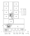
- FIG. 1 is a plan view illustrating a joint system according to one embodiment.
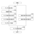
- FIG. 2 is a flow chart illustrating a bonding method according to one embodiment.
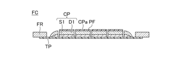
- FIG. 3 is a cross-sectional view showing an example of a first chip carrier and a chip.
- FIG. 4 is a cross-sectional view showing an example of the second chip carrier.
- FIG. 5 is a cross-sectional view showing an example of a second chip carrier and a chip.
- FIG. 6 is a cross-sectional view showing an example of a substrate.
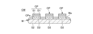
- FIG. 7 is a cross-sectional view showing an example of a substrate with chips.
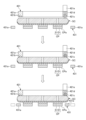
- FIG. 8 is a cross-sectional view showing an example of the operation of the chip array device.
- FIG. 9 is a cross-sectional view showing an example of electrostatic attraction.
- FIG. 10 is a cross-sectional view showing an example of the operation of the joining device.
- FIG. 11 is a cross-sectional view showing an example of the operation subsequent to that shown in FIG.
- FIG. 12 is a plan view showing an example of the movement range of a chip carrier holder and the movement range of a substrate holder in the bonding device.
- FIG. 13 is a plan view showing a modification of FIG.
- FIG. 14 is a cross-sectional view showing an example of a chip carrier holding portion of a bonding apparatus.
- FIG. 15 is a bottom view showing an example of a chip carrier holding portion of a bonding apparatus.
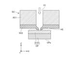
- FIG. 16 is a cross-sectional view showing an example of the adsorption operation.
- FIG. 17 is a cross-sectional view showing an example of the peeling operation.
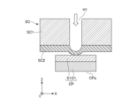
- FIG. 18 is a cross-sectional view showing a modification of FIG.
- the X-axis direction, the Y-axis direction, and the Z-axis direction are perpendicular to each other.
- the X-axis direction and the Y-axis direction are horizontal directions, and the Z-axis direction is vertical.
- the bonding system 1 manufactures a chip-equipped substrate CW by bonding a chip CP to a substrate W.
- the chip-equipped substrate CW includes a substrate W and a plurality of chips CP bonded to the substrate W.
- the chip CP has a base substrate S1 and a device D1 formed on the base substrate S1.
- the base substrate S1 is, for example, a silicon wafer, a compound semiconductor wafer, or a glass substrate.
- the device D1 includes a semiconductor element, a circuit, or a terminal.
- the device D1 is formed on the bonding surface CPa of the chip CP.
- the substrate W has a base substrate S2 and a plurality of devices D2 formed on the base substrate S2.
- the base substrate S2 is, for example, a silicon wafer, a compound semiconductor wafer, or a glass substrate.
- the devices D2 include semiconductor elements, circuits, terminals, or the like.
- the devices D2 are formed on the bonding surface Wa of the substrate W.
- the device D1 of the chip CP and the device D2 of the substrate W are electrically connected. Although not shown, multiple devices D1 may be electrically connected to one device D2. Here, the multiple devices D1 may have different functions, i.e., different electrical circuits.
- the device D1 of one chip CP may be electrically connected to the device D2 of the substrate W via the device D1 of another chip CP.
- the joining system 1 includes a loading/unloading station 2, a processing station 3, and a control circuit 9.
- the loading/unloading station 2 and the processing station 3 are arranged in this order from the negative side of the X-axis to the positive side of the X-axis.
- the loading/unloading station 2 includes a mounting table 20.
- Cassettes C1 to C6 are mounted on the mounting table 20.
- Cassette C1 accommodates multiple chips CP held in a first chip carrier FC.
- Cassette C2 accommodates a used first chip carrier FC from which at least some of the chips CP have been removed.
- Cassettes C3 and C4 accommodate second chip carriers SC.
- Cassette C5 accommodates a substrate W prior to bonding with a chip CP.
- Cassette C6 accommodates a substrate CW with a chip attached.
- the first chip carrier FC has a tape TP to which the chips CP are adhered, and a frame FR to which the outer periphery of the tape TP is adhered.
- Multiple chips CP are arranged in the opening of the frame FR.
- the multiple chips CP are obtained, for example, by dicing a substrate while the substrate is adhered to the tape TP.
- the bonding surface CPa of the chips CP is protected by a protective film PF before dicing.
- the protective film PF is positioned on the opposite side of the chips CP from the tape TP.
- the protective film PF is removed before bonding the chips CP to the substrate W.
- the second chip carrier SC holds multiple chips CP that have been removed from the first chip carrier FC.
- the second chip carrier SC is, for example, an electrostatic carrier.
- the electrostatic carrier electrostatically adsorbs the multiple chips CP.
- the electrostatic carrier may also electrostatically adsorb the multiple chips CP and vacuum adsorb them. Even after the electrostatic adsorption force disappears, it is possible to continue to hold the multiple chips CP by the vacuum adsorption force.
- the second chip carrier SC does not have to be an electrostatic carrier, as will be described in more detail later.
- the second chip carrier SC holds multiple chips CP with the same function, but it may also hold multiple chips CP with different functions.
- multiple first chip carriers FC are prepared according to the functions of the chip CP. It is also possible to transfer multiple chips CP with different functions from multiple first chip carriers FC to one second chip carrier SC.
- the chip CP is transferred from the first chip carrier FC to the second chip carrier SC in order to remove the protective film PF from the chip CP and modify the bonding surface CPa of the chip CP before bonding the chip CP to the substrate W. This is to prevent the tape TP of the first chip carrier FC from being damaged when modifying the bonding surface CPa. Details of the second chip carrier SC will be described later.
- the loading/unloading station 2 comprises a transport area 21, a first chip carrier transport arm 22, a second chip carrier transport arm 23, and a substrate transport arm 24.
- the first chip carrier transport arm 22, the second chip carrier transport arm 23, and the substrate transport arm 24 may be collectively referred to as transport arms 22 to 24.
- the transport area 21 is adjacent to the mounting table 20.
- the transport arms 22 to 24 hold and transport the first chip carrier FC, the second chip carrier SC, or the substrate W.
- Each of the transport arms 22 to 24 is capable of moving horizontally (in both the X-axis and Y-axis directions) and vertically, and of rotating around a vertical axis.
- the transport device is made up of the transport arms 22 to 24 and a drive unit (not shown) that moves or rotates the transport arms 22 to 24.
- the transport arms 22 to 24 may be mounted on the same Y-axis slider and moved simultaneously in the Y-axis direction as shown in FIG. 1, or may be mounted on different Y-axis sliders and moved independently in the Y-axis direction.
- the transport arms 22 to 24 are positioned at different heights.
- the loading/unloading station 2 is equipped with a transition device 25 on the opposite side of the transfer area 21 from the mounting table 20.
- the transition device 25 is provided between the transfer area 21 of the loading/unloading station 2 and the transfer area 31 of the processing station 3, and relays the first chip carrier FC, the second chip carrier SC or the substrate W between them.
- Multiple transition devices 25 may be stacked in the Z-axis direction.
- the processing station 3 comprises a transport area 31, a first chip carrier transport arm 32, a second chip carrier transport arm 33, and a substrate transport arm 34.
- the first chip carrier transport arm 32, the second chip carrier transport arm 33, and the substrate transport arm 34 may be collectively referred to as transport arms 32 to 34.
- the transport area 31 extends in the X-axis direction.
- the transport arms 32 to 34 hold and transport the first chip carrier FC, the second chip carrier SC, or the substrate W.
- Each of the transport arms 32 to 34 is capable of moving horizontally (in both the X-axis and Y-axis directions) and vertically, and of rotating around a vertical axis.
- the transport device is made up of the transport arms 32 to 34 and a drive unit (not shown) that moves or rotates the transport arms 32 to 34.
- the transport arms 32 to 34 may be mounted on the same X-axis slider and moved simultaneously in the X-axis direction as shown in FIG. 1, or may be mounted on different X-axis sliders and moved independently in the X-axis direction.
- the transport arms 32 to 34 are positioned at different heights.
- the processing station 3 includes a chip arrangement device 35, a cleaning device 36, a first activation device 37, a first hydrophilization device 38, an inversion device 39, a second activation device 40, a second hydrophilization device 41, and a bonding device 42. These devices 35 to 42 are adjacent to the transport area 31, and are disposed on the positive Y-axis side or the negative Y-axis side of the transport area 31, respectively.
- the chip arrangement device 35 transfers the chip CP from the first chip carrier FC to the second chip carrier SC. This prevents damage to the tape TP of the first chip carrier FC when modifying the bonding surface CPa. Details of the chip arrangement device 35 will be described later.
- the cleaning device 36 removes the protective film PF from the chip CP while the chip CP is held by the second chip carrier SC.
- the cleaning device 36 also cleans the bonding surface CPa of the chip CP. This improves the quality of the subsequent processing of the bonding surface CPa.
- the first activation device 37 activates the bonding surface CPa of the chip CP while the chip CP is held by the second chip carrier SC.
- the first activation device 37 is, for example, a plasma processing device.
- oxygen gas which is a processing gas
- the bonding surface CPa of the chip CP is activated by irradiating the oxygen ions onto the bonding surface CPa of the chip CP.
- the processing gas is not limited to oxygen gas, and may be, for example, nitrogen gas, etc.
- the first hydrophilization device 38 hydrophilizes the bonding surface CPa of the chip CP while the chip CP is held by the second chip carrier SC.
- the first hydrophilization device 38 supplies pure water (e.g., deionized water) onto the chip CP while rotating the second chip carrier SC held by the spin chuck.
- the pure water imparts OH groups to the bonding surface CPa of the chip CP, which has been activated in advance.
- the hydrogen bonds between the OH groups can be used to bond the chip CP to the substrate W.
- the inversion device 39 inverts the second chip carrier SC upside down while the chip CP is held by the second chip carrier SC. It can invert multiple chips CP upside down all at once, and the bonding surface CPa of each chip CP can face downward.
- the inversion device 39 may be provided inside the bonding device 42.
- the second activation device 40 activates the bonding surface Wa of the substrate W.
- the second activation device 40 is, for example, a plasma processing device.
- oxygen gas which is a processing gas
- the bonding surface Wa of the substrate W is activated by irradiating the oxygen ions onto the bonding surface Wa of the substrate W.
- the processing gas is not limited to oxygen gas, and may be, for example, nitrogen gas, etc.
- the second hydrophilization device 41 hydrophilizes the bonding surface Wa of the substrate W.
- the second hydrophilization device 41 supplies pure water (e.g., deionized water) onto the substrate W while rotating the substrate W held by the spin chuck.
- the pure water imparts OH groups to the bonding surface Wa of the substrate W, which has been activated in advance.
- the chip CP and the substrate W can be bonded by utilizing hydrogen bonds between the OH groups.
- the bonding device 42 removes the chip CP from the second chip carrier SC, and bonds the chip CP to the substrate W by orienting the bonding surface CPa of the removed chip CP toward the bonding surface Wa of the substrate W.
- a substrate CW with a chip is obtained.
- the device D1 of the chip CP and the device D2 of the substrate W are electrically connected. Details of the bonding device 42 will be described later.
- the control circuit 9 is, for example, a computer, and includes an arithmetic unit 91 such as a CPU (Central Processing Unit), and a storage unit 92 such as a memory.
- the storage unit 92 stores programs that control various processes executed in the bonding system 1.
- the control circuit 9 controls the operation of the bonding system 1 by having the arithmetic unit 91 execute the programs stored in the storage unit 92.
- a lower control circuit that controls the operation of each device constituting the bonding system 1 may be provided, and a higher-level control circuit that controls multiple lower-level control circuits may be provided.
- the control circuit 9 may be composed of the lower-level control circuit and the higher-level control circuit.
- the control circuit 9 includes electronic circuits such as a CPU, FPGA (Field Programmable Gate Array) or ASIC (Application Specific Integrated Circuit), and executes the various control operations described in this specification by executing instruction codes stored in memory or by being a circuit designed for a specific purpose.
- electronic circuits such as a CPU, FPGA (Field Programmable Gate Array) or ASIC (Application Specific Integrated Circuit)
- the first chip carrier transport arm 22 takes out the first chip carrier FC and multiple chips CP from the cassette C1 and transports them to the transition device 25.
- the first chip carrier transport arm 32 takes out the first chip carrier FC and multiple chips CP from the transition device 25 and transports them to the chip arrangement device 35.
- the second chip carrier transport arm 23 also removes the second chip carrier SC from the cassette C3 and transports it to the transition device 25.
- the second chip carrier transport arm 33 removes the second chip carrier SC from the transition device 25 and transports it to the chip arrangement device 35.
- the chip arrangement device 35 transfers the chips CP from the first chip carrier FC to the second chip carrier SC (step S101).
- the second chip carrier transport arm 33 removes the multiple chips CP together with the second chip carrier SC from the chip arrangement device 35 and transports them to the cleaning device 36.
- the cleaning device 36 removes the protective film PF from the chip CP while the chip CP is held by the second chip carrier SC (step S102).
- the second chip carrier transport arm 33 takes out the multiple chips CP together with the second chip carrier SC from the cleaning device 36 and transports them to the first activation device 37.
- the first activation device 37 activates the bonding surface CPa of the chip CP while the chip CP is held by the second chip carrier SC (step S103).
- the second chip carrier transport arm 33 takes out the multiple chips CP together with the second chip carrier SC from the first activation device 37 and transports them to the first hydrophilization device 38.
- the first hydrophilization device 38 hydrophilizes the bonding surface CPa of the chip CP while the chip CP is held by the second chip carrier SC (step S104).
- the second chip carrier transport arm 33 takes out the multiple chips CP together with the second chip carrier SC from the first hydrophilization device 38 and transports them to the inversion device 39.
- the inversion device 39 inverts the second chip carrier SC upside down while the second chip carrier SC holds the chips CP (step S105).
- the second chip carrier transport arm 33 takes out the second chip carrier SC together with the multiple chips CP from the inversion device 39 and transports them to the bonding device 42.
- the substrate transport arm 24 removes the substrate W from the cassette C5 and transports it to the transition device 25. Then, the substrate transport arm 34 removes the substrate W from the transition device 25 and transports it to the second activation device 40.
- the second activation device 40 activates the bonding surface Wa of the substrate W (step S106).
- the substrate transport arm 34 removes the substrate W from the second activation device 40 and transports it to the second hydrophilization device 41.
- the second hydrophilization device 41 hydrophilizes the bonding surface Wa of the substrate W (step S107).
- the substrate transport arm 34 removes the substrate W from the second hydrophilization device 41 and transports it to the bonding device 42.
- the bonding device 42 removes the chip CP from the second chip carrier SC, and bonds the chip CP to the substrate W by orienting the bonding surface CPa of the removed chip CP toward the bonding surface Wa of the substrate W (step S108).
- the substrate CW with a chip may be heated by an annealing device (not shown) to improve the bonding strength between the chip CP and the substrate W.
- the substrate transport arm 34 removes the chip-attached substrate CW from the bonding device 42 and transports it to the transition device 25.
- the substrate transport arm 24 removes the chip-attached substrate CW from the transition device 25 and stores it in the cassette C6. The chip-attached substrate CW is transported out of the bonding system 1 while still stored in the cassette C6.
- the second chip carrier transport arm 33 removes the second chip carrier SC from the bonding device 42 and transports it to the transition device 25. After that, the second chip carrier transport arm 23 removes the second chip carrier SC from the transition device 25 and stores it in the cassette C4.
- the first chip carrier transport arm 32 removes the first chip carrier FC from the chip arrangement device 35 and transports it to the transition device 25.
- the first chip carrier transport arm 22 removes the first chip carrier FC from the transition device 25 and stores it in the cassette C2.
- the chip arrangement device 35 transfers the chip CP from the first chip carrier FC to the second chip carrier SC. This allows the use of a chip carrier with relatively excellent durability when modifying the bonding surface CPa.
- the second chip carrier SC is not particularly limited as long as it has superior durability compared to the first chip carrier FC, but may be, for example, an electrostatic carrier.
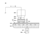
- the electrostatic carrier has, for example, a conductive substrate SC1 and an insulating film SC2, and electrostatically attracts the chip CP to the side opposite the conductive substrate SC1 with the insulating film SC2 as a reference.
- the conductive substrate SC1 is made of, for example, silicon, aluminum, an aluminum alloy, stainless steel, or titanium. As shown in Figures 4 and 5, the conductive substrate SC1 may have one or more through holes H1 formed for each chip CP.
- the chip CP can be peeled off from the second chip carrier SC by supplying gas to the through hole H1 or by inserting a pin (not shown) into the through hole H1.
- the number and arrangement of the through holes H1 are not particularly limited.
- the insulating film SC2 maintains the electrostatic adsorption force by restricting the movement of charge between the base substrate S1 of the chip CP and the conductive substrate SC1.
- the insulating film SC2 preferably has a breakdown voltage of 30 kV or more, and more preferably 40 kV or more.
- the insulating film SC2 is preferably made of a flexible material, specifically a material with an elastic modulus of 2 GPa or less, more preferably 0.5 GPa or less. From the viewpoint of durability when modifying the bonding surface CPa, for example, polyimide or EVA (ethylene-vinyl acetate copolymer) is used.
- the thickness of the insulating film SC2 is, for example, 10 ⁇ m.
- the insulating film SC2 may have a through hole H2 formed therein, which is connected to the through hole H1 in the conductive substrate SC1. As shown in FIG. 17, it is preferable that the diameter of the through hole H2 in the insulating film SC2 is smaller than the diameter of the through hole H1 in the conductive substrate SC1. Note that, as shown in FIG. 18, the through hole H2 may not be present.
- the second chip carrier SC preferably has the same diameter as the substrate W.
- the second chip carrier transport arm 23 and the substrate transport arm 24 can be of the same model number (i.e., the same dimensions and shape), reducing costs.
- the second chip carrier transport arm 33 and the substrate transport arm 34, the first activation device 37 and the second activation device 40, or the first hydrophilization device 38 and the second hydrophilization device 41 can also be of the same model number, reducing costs. This also prevents the device from becoming too large.
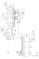
- the chip arrangement device 35 includes a first chip carrier holding part 351, a pressing part 352, a second chip carrier holding part 353, and a chip transport mechanism 354.
- the first chip carrier holding part 351 holds the first chip carrier FC from below the first chip carrier FC.
- the first chip carrier FC holds the chip CP with the bonding surface CPa of the chip CP facing upward.
- the first chip carrier holding part 351 holds the frame FR of the first chip carrier FC, and allows deformation of the tape TP at the opening of the frame FR.
- the pressing portion 352 locally presses the chip CP through the tape TP and locally deforms the tape TP.
- the chips CP can be pushed up individually, and when the chips CP are picked up, the chips CP can be prevented from rubbing against each other.
- the pressing portion 352 and the first chip carrier holding portion 351 can move relative to each other, and the position at which the chip CP is pushed up can be changed.
- the second chip carrier holding section 353 holds the second chip carrier SC from below the second chip carrier SC.
- the second chip carrier SC holds the chip CP with the bonding surface CPa of the chip CP facing upward.
- the first chip carrier FC holds the chip CP with the bonding surface CPa of the chip CP facing upward. Therefore, the chip transport mechanism 354 also transports the chip CP with the bonding surface CPa of the chip CP facing upward. The chip transport mechanism 354 does not turn the chip CP upside down.
- the chip transport mechanism 354 has a suction head 355 that suctions the chip CP.
- the suction head 355 is positioned above the chip CP.
- the bonding surface CPa of the chip CP is covered with a protective film PF, and the suction head 355 suctions the chip CP via the protective film PF.
- the suction head 355 comes into contact with the protective film PF, but does not come into contact with the chip CP. This makes it possible to suppress damage to the chip CP.
- the chip arrangement device 35 includes a charge supply unit 356 and a charge removal unit 358.
- the charge supply unit 356 supplies a charge of a first polarity (e.g., positive) to the conductive substrate SC1 by applying a voltage to the conductive substrate SC1.
- the charge removal unit 358 removes the charge of the first polarity from the chip CP, leaving a charge of a second polarity (e.g., negative) that is opposite to the first polarity on the chip CP.
- a charge of a first polarity accumulates on the conductive substrate SC1, while a charge of a second polarity accumulates on the chip CP.
- a potential difference occurs between the conductive substrate SC1 and the chip CP across the insulating film SC2, generating an electrostatic adsorption force.
- the generated electrostatic adsorption force is maintained even after the application of voltage to the conductive substrate SC1 and the de-electrification of the chip CP are released.
- the charge supply unit 356 has, for example, a power supply pin 357 that contacts the conductive substrate SC1.
- the power supply pin 357 is provided, for example, on the second chip carrier holding unit 353 and is electrically connected to a power source (not shown).
- the charge removal unit 358 has, for example, an earth wire 359.
- the earth wire 359 removes the charge of the first polarity from the chip CP via, for example, the protective film PF.
- the earth wire 359 is embedded in the suction head 355, but it may be provided separately from the suction head 355.
- the chips CP are electrostatically attracted one by one, but multiple chips CP may be arranged on the insulating film SC2 and then electrostatically attracted simultaneously.
- the insulating film SC2 is made of a flexible material.
- the insulating film SC2 deforms so that air escapes from between the chip CP and the insulating film SC2, and a vacuum adsorption force is generated between the chip CP and the insulating film SC2.
- the second chip carrier SC is an electrostatic carrier having a conductive substrate SC1 and an insulating film SC2, but it does not have to be an electrostatic carrier.
- the second chip carrier SC may have a carrier substrate and a resin film provided on the surface of the carrier substrate facing the chip CP.
- the second chip carrier SC holds multiple chips CP on the resin film.
- the carrier substrate may be conductive like the conductive substrate SC1, or may be insulating like the conductive substrate SC1.
- the carrier substrate is preferably made of a material having rigidity.
- the carrier substrate is preferably made of silicon (Si), ceramic, aluminum, aluminum alloy, stainless steel, zirconia, silicon carbide (SiC), titanium, or glass.
- the carrier substrate may have a diameter similar to that of the substrate W.
- the carrier substrate may also have a thickness similar to that of the substrate W.
- the carrier substrate may have a through hole H1 like the conductive substrate SC1.
- the resin film may be insulating like the insulating film SC2, or may be conductive like the insulating film SC2.
- the resin film is preferably made of a flexible material, specifically a material with an elastic modulus of 2 GPa or less, more preferably 0.5 GPa or less. From the viewpoint of durability when modifying the bonding surface of the chip CP, the resin film is preferably made of, for example, polyimide or EVA (ethylene-vinyl acetate copolymer).
- the thickness of the resin film is, for example, 10 ⁇ m.
- the resin film may be a single layer or multiple layers.
- the resin film may have a polyolefin layer and an acrylic adhesive layer.
- the resin film may have a through hole H2 like the insulating film SC2.
- the bonding device 42 removes the chip CP from the second chip carrier SC, and bonds the chip CP to the substrate W by orienting the bonding surface CPa of the removed chip CP toward the bonding surface Wa of the substrate W.
- a substrate CW with a chip is obtained.
- the device D1 of the chip CP and the device D2 of the substrate W are electrically connected.
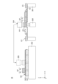
- the bonding device 42 includes, for example, a chip carrier holding section 421, a substrate holding section 422, a first chip transport mechanism 423, and a second chip transport mechanism 424.
- the chip carrier holding section 421 holds the second chip carrier SC from above the second chip carrier SC with the bonding surface CPa of each of the multiple chips CP held in the second chip carrier SC facing downward.
- the substrate holding section 422 holds the substrate W from below the substrate W with the bonding surface Wa of the substrate W facing upward.
- the first chip transport mechanism 423 receives the chip CP from the second chip carrier SC and transports the chip CP with the bonding surface CPa of the chip CP facing downward.
- the second chip transport mechanism 424 receives the chip CP from the first chip transport mechanism 423 and bonds the chip CP to the substrate W with the bonding surface CPa of the chip CP facing downward.
- the inversion device 39 inverts the second chip carrier SC upside down.
- a plurality of chips CP can be inverted upside down all at once in advance, and the bonding surface CPa of each chip CP can face downward.
- the first chip transport mechanism 423 and the second chip transport mechanism 424 do not invert the chips CP upside down individually while transporting them individually. This makes it possible to eliminate the mechanism that inverts the chips CP upside down individually, and thus suppresses dust generation from that mechanism.
- the structure of the first chip transport mechanism 423 and the second chip transport mechanism 424 can be simplified. Furthermore, the number of inversions can be reduced, improving dust generation and throughput.
- the chip carrier holding part 421 holds the second chip carrier SC from above the second chip carrier SC
- the substrate holding part 422 holds the substrate W from below the substrate W.
- the accuracy of the bonding position is mainly determined by the alignment accuracy of the second chip transport mechanism 424 and the substrate holding part 422. Compared to this alignment accuracy, the alignment accuracy of the first chip transport mechanism 423 and the chip carrier holding part 421 may be lower. Therefore, even if the chip carrier holding part 421 holds the second chip carrier SC from above the second chip carrier SC, the accuracy of the bonding position does not deteriorate.
- the chip carrier holding unit 421 holds the second chip carrier SC, but may also hold the first chip carrier FC. If the bonding system 1 does not modify the bonding surface CPa of the chip CP, there is no need to transfer the chip CP from the first chip carrier FC to the second chip carrier SC. Therefore, the chip carrier holding unit 421 may hold the first chip carrier FC.
- the inversion device 39 simply inverts the first chip carrier FC upside down. Multiple chips CP can be inverted upside down all at once in advance, and the bonding surface CPa of each chip CP can face downward. This eliminates the need for a mechanism for individually inverting the chips CP upside down, and reduces dust generation from that mechanism.
- the structure of the first chip transport mechanism 423 and the second chip transport mechanism 424 can be simplified. Furthermore, the number of inversions can be reduced, improving dust generation and throughput. Furthermore, the precision of the bonding position between the chip CP and the substrate W can be improved.
- the first chip transport mechanism 423 has, for example, a first suction head 423a and a first drive unit 423b.
- the first suction head 423a is disposed below the chip CP and adsorbs the bonding surface CPa of the chip CP.
- the first suction head 423a is movable, for example, in the X-axis direction and the Z-axis direction.
- the first drive unit 423b moves the first suction head 423a.
- the first suction head 423a preferably suctions the bonding surface CPa of the chip CP without contact.
- the first suction head 423a preferably suctions the bonding surface CPa of the chip CP while leaving a gap between it and the chip CP. This can prevent contamination of the bonding surface CPa of the chip CP.
- the first suction head 423a is, for example, an ultrasonic or Bernoulli type.
- the ultrasonic type uses the squeeze effect caused by ultrasonic vibrations, while the Bernoulli type uses the Bernoulli effect.
- the ultrasonic type can suppress horizontal deviations more than the Bernoulli type.
- the second chip transport mechanism 424 has, for example, a second suction head 424a and a second drive unit 424b.
- the second suction head 424a is positioned above the chip CP and suctions the back surface CPb of the chip CP, which faces the opposite side to the bonding surface CPa. Since it is not a problem if the back surface CPb becomes dirty, the second suction head 424a comes into contact with the chip CP.
- the second suction head 424a can move, for example, in the X-axis direction, the Y-axis direction, the Z-axis direction, and the ⁇ direction.
- the ⁇ direction is the circumferential direction of the vertical center line of rotation. In other words, the second suction head 424a may rotate around the vertical center line of rotation.
- the second drive unit 424b moves the second suction head 424a.
- the bonding device 42 may be equipped with at least one of a first imaging section 425, a second imaging section 426, and a third imaging section 427 to improve the accuracy of the bonding position of the chip CP and the substrate W.
- the first imaging section 425, the second imaging section 426, and the third imaging section 427 do not have to capture an image every time the chip CP and the substrate W are bonded, and may capture images periodically.
- the first imaging unit 425 images the alignment marks on the bonding surface CPa of the chip CP held by the second suction head 424a.
- the number of alignment marks to be imaged is, for example, two, but is not particularly limited.
- the alignment marks may be dedicated marks or may be part of the electrical circuit that constitutes the device D1.
- the first imaging unit 425 is disposed below the second suction head 424a.
- the first imaging unit 425 transmits the captured image to the control circuit 9.
- the control circuit 9 detects the position of the chip CP in the first coordinate system set for the second suction head 424a by processing the image captured by the first imaging unit 425.
- the second imaging unit 426 captures an image of the alignment marks on the bonding surface Wa of the substrate W held by the substrate holding unit 422.
- the number of alignment marks captured is, for example, two, but is not limited thereto.
- the alignment marks may be dedicated marks or may be part of the electrical circuit that constitutes the device D2.
- the second imaging unit 426 is disposed above the substrate holding unit 422, for example, on the second suction head 424a.
- the second imaging unit 426 transmits the captured image to the control circuit 9.
- the control circuit 9 detects the position of the device D2 in the second coordinate system set on the substrate holding unit 422 by processing the image captured by the second imaging unit 426.
- the control circuit 9 uses images captured by at least one of the first imaging unit 425 and the second imaging unit 426 to align the chip CP held by the second suction head 424a with the substrate W held by the substrate holder 422. Before bonding the chip CP and substrate W, the position of the chip CP or substrate W can be corrected, improving the accuracy of the bonding position.
- the third imaging unit 427 After bonding the chip CP and the substrate W, the third imaging unit 427 simultaneously images both the alignment mark on the bonding surface CPa of the chip CP and the alignment mark on the bonding surface Wa of the substrate W.
- the third imaging unit 427 images the alignment marks of the chip CP and the substrate W by transmitting light through the chip CP or the substrate W (chip CP in this embodiment).
- the third imaging unit 427 is composed of, for example, an infrared camera.
- the third imaging unit 427 When capturing an image of the alignment marks of the chip CP and the substrate W through the chip CP, the third imaging unit 427 is disposed above the substrate holding unit 422, for example, on the second suction head 424a.
- the third imaging unit 427 transmits the captured image to the control circuit 9.
- the control circuit 9 detects the deviation between the actual bonding position and the target bonding position by processing the image captured by the third imaging unit 427.
- the control circuit 9 uses the image captured by the third imaging unit 427 to align the chip CP held by the second suction head 424a with the substrate W held by the substrate holder 422 in the next and subsequent bonding of the chip CP and substrate W.
- the position of the chip CP or substrate W can be corrected taking into account the characteristics of the bonding device 42, improving the accuracy of the bonding position.
- the bonding device 42 may include a first moving unit 428 and a second moving unit 429.
- the first moving unit 428 moves the chip carrier holding unit 421 in the horizontal direction.
- the first moving unit 428 may move the chip carrier holding unit 421 in the vertical direction.
- the second moving unit 429 moves the substrate holding unit 422 in the horizontal direction.
- the second moving unit 429 may move the substrate holding unit 422 in the vertical direction.
- the chip carrier holding part 421 holds the second chip carrier SC from above the second chip carrier SC
- the substrate holding part 422 holds the substrate W from below the substrate W. Therefore, it is possible to arrange the second chip carrier SC and the substrate W at different heights. Therefore, it is possible to arrange the chip carrier holding part 421 and the substrate holding part 422 at different heights.
- the substrate holding part 422 is movable in a horizontal first axis direction and a horizontal second axis direction perpendicular to the first axis direction.
- the first axis direction is, for example, the X axis direction
- the second axis direction is, for example, the Y axis direction.
- the substrate holding part 422 is movable in both the X axis positive direction and the X axis negative direction.
- the substrate holding part 422 is also movable in both the Y axis positive direction and the Y axis positive direction.
- the chip carrier holding part 421 may be movable in both the first and second axial directions as shown in FIG. 12, or may be movable only in the second axial direction out of the first and second axial directions as shown in FIG. 13. In the latter case, as shown in FIG. 13, the movement range of the chip carrier holding part 421 and the movement range of the substrate holding part 422 may overlap in the first axial direction when the chip carrier holding part 421 is viewed from above. In the latter case, the footprint of the bonding device 42 can be made smaller than in the former case.
- the bonding device 42 may include a pressing mechanism 430.
- the pressing mechanism 430 presses the chip CP downward against the second chip carrier SC held by the chip carrier holding portion 421.
- the pressing mechanism 430 presses the chips CP downward individually, and peels the chips CP individually from the second chip carrier SC.
- the pressing mechanism 430 peels off the chip CP from the second chip carrier SC, for example, by supplying gas to the through hole H1 of the conductive substrate SC1 or by inserting a pin (not shown) into the through hole H1.
- the number and arrangement of the through holes H1 are not particularly limited.
- the insulating film SC2 may have a through hole H2 as shown in FIG. 17, or may not have a through hole H2 as shown in FIG. 18.
- the chip carrier holding portion 421 may adsorb only a portion of the upper surface of the second chip carrier SC.
- the pressing mechanism 430 can press the chip CP downward on the remaining portion of the upper surface of the second chip carrier SC.
- the second chip carrier SC can be held from above the second chip carrier SC, and the chip CP held by the second chip carrier SC can be pressed downward.
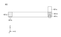
- the chip carrier holding portion 421 has, for example, a ring portion 421a.
- the ring portion 421a adsorbs the outer periphery of the upper surface of the second chip carrier SC.
- the pressing mechanism 430 can press the chip CP downward at the center of the upper surface of the second chip carrier SC.
- a groove 421b for vacuum adsorption, for example, is formed on the lower surface of the ring portion 421a.
- a hole may be formed instead of the groove 421b.
- the chip carrier holding portion 421 may have a second ring portion concentric with the ring portion 421a inside the ring portion 421a.
- the chip carrier holding portion 421 may also have a radial or lattice-shaped rib portion inside the ring portion 421a.
- the second ring portion and the rib portion may be provided in combination. It is sufficient that the pressing mechanism 430 can press the chip CP downward.
- the chip carrier holding portion 421 may have a pad portion 421c.
- a plurality of pad portions 421c are provided at intervals along the outer periphery of the top surface of the second chip carrier SC.
- the pad portions 421c adsorb the outer periphery of the top surface of the second chip carrier SC. Therefore, the pressing mechanism 430 can press the chip CP downward at the center of the top surface of the second chip carrier SC.
- a through hole 421d is formed in the ring portion 421a, and the pad portion 421c is disposed in the through hole 421d.
- a notch may be formed instead of the through hole 421d. Note that, although the ring portion 421a and the pad portion 421c are used in combination in this embodiment, either one of them may be used alone.
- the pad portion 421c may expand and contract in the vertical direction.
- the structure of the pad portion 421c is a bellows, but it may also be telescopic.
- the pad portion 421c contracts, allowing the ring portion 421a to adsorb the upper surface of the second chip carrier SC.
- the second chip carrier SC can be smoothly transferred between the transport device and the ring portion 421a.
- the chip carrier holding portion 421 may have a lifting portion 421e.
- the lifting portion 421e raises and lowers the pad portion 421c relative to the ring portion 421a. After the pad portion 421c adsorbs the top surface of the second chip carrier SC, the pad portion 421c is raised, allowing the ring portion 421a to adsorb the top surface of the second chip carrier SC.
- the lifting portion 421e is composed of, for example, a pneumatic cylinder or an electric cylinder.
- the bonding device 42 may be provided with a fall restriction mechanism 431.
- the fall restriction mechanism 431 restricts the second chip carrier SC from falling downward from the chip carrier holding portion 421.
- the fall restriction mechanism 431 has, for example, multiple movable parts 431a and a drive part (not shown) that moves the multiple movable parts 431a between an open position and a closed position.
- the open position is a position that allows the second chip carrier SC to rise and fall.
- the closed position is a position that restricts the fall of the second chip carrier SC.
- the chip carrier holding portion 421 holds the second chip carrier SC, but as described above, it may also hold the first chip carrier FC. In the latter case, the ring portion 421a and the pad portion 421c adsorb the outer periphery of the first chip carrier FC, specifically the frame FR.
- Bonding system 42 Bonding device 421 Chip carrier holding section 422 Substrate holding section 423 First chip transport mechanism 424 Second chip transport mechanism CP Chip SC Second chip carrier (chip carrier) W substrate
Landscapes
- Wire Bonding (AREA)
- Container, Conveyance, Adherence, Positioning, Of Wafer (AREA)
- Die Bonding (AREA)
Priority Applications (2)
| Application Number | Priority Date | Filing Date | Title |
|---|---|---|---|
| KR1020257039934A KR20260003212A (ko) | 2023-05-02 | 2024-04-18 | 접합 장치, 접합 시스템, 및 접합 방법 |
| JP2025518124A JPWO2024228335A1 (cg-RX-API-DMAC7.html) | 2023-05-02 | 2024-04-18 |
Applications Claiming Priority (2)
| Application Number | Priority Date | Filing Date | Title |
|---|---|---|---|
| JP2023076345 | 2023-05-02 | ||
| JP2023-076345 | 2023-05-02 |
Publications (1)
| Publication Number | Publication Date |
|---|---|
| WO2024228335A1 true WO2024228335A1 (ja) | 2024-11-07 |
Family
ID=93333037
Family Applications (1)
| Application Number | Title | Priority Date | Filing Date |
|---|---|---|---|
| PCT/JP2024/015435 Ceased WO2024228335A1 (ja) | 2023-05-02 | 2024-04-18 | 接合装置、接合システム、及び接合方法 |
Country Status (4)
| Country | Link |
|---|---|
| JP (1) | JPWO2024228335A1 (cg-RX-API-DMAC7.html) |
| KR (1) | KR20260003212A (cg-RX-API-DMAC7.html) |
| TW (1) | TW202447814A (cg-RX-API-DMAC7.html) |
| WO (1) | WO2024228335A1 (cg-RX-API-DMAC7.html) |
Citations (5)
| Publication number | Priority date | Publication date | Assignee | Title |
|---|---|---|---|---|
| JP2012234952A (ja) * | 2011-04-28 | 2012-11-29 | Shibaura Mechatronics Corp | 電子部品の実装装置及び実装方法 |
| JP2013243333A (ja) * | 2012-04-24 | 2013-12-05 | Tadatomo Suga | チップオンウエハ接合方法及び接合装置並びにチップとウエハとを含む構造体 |
| CN213366559U (zh) * | 2020-11-17 | 2021-06-04 | 武汉新芯集成电路制造有限公司 | 静电吸盘 |
| JP2022153687A (ja) * | 2021-03-30 | 2022-10-13 | 東レエンジニアリング株式会社 | チップ搬送装置およびこれを用いた実装装置ならびに実装方法 |
| JP2023045346A (ja) * | 2021-09-22 | 2023-04-03 | ファスフォードテクノロジ株式会社 | ディッピング装置、ダイボンディング装置および半導体装置の製造方法 |
Family Cites Families (1)
| Publication number | Priority date | Publication date | Assignee | Title |
|---|---|---|---|---|
| US9142532B2 (en) | 2012-04-24 | 2015-09-22 | Bondtech Co., Ltd. | Chip-on-wafer bonding method and bonding device, and structure comprising chip and wafer |
-
2024
- 2024-04-18 JP JP2025518124A patent/JPWO2024228335A1/ja active Pending
- 2024-04-18 KR KR1020257039934A patent/KR20260003212A/ko active Pending
- 2024-04-18 WO PCT/JP2024/015435 patent/WO2024228335A1/ja not_active Ceased
- 2024-04-25 TW TW113115415A patent/TW202447814A/zh unknown
Patent Citations (5)
| Publication number | Priority date | Publication date | Assignee | Title |
|---|---|---|---|---|
| JP2012234952A (ja) * | 2011-04-28 | 2012-11-29 | Shibaura Mechatronics Corp | 電子部品の実装装置及び実装方法 |
| JP2013243333A (ja) * | 2012-04-24 | 2013-12-05 | Tadatomo Suga | チップオンウエハ接合方法及び接合装置並びにチップとウエハとを含む構造体 |
| CN213366559U (zh) * | 2020-11-17 | 2021-06-04 | 武汉新芯集成电路制造有限公司 | 静电吸盘 |
| JP2022153687A (ja) * | 2021-03-30 | 2022-10-13 | 東レエンジニアリング株式会社 | チップ搬送装置およびこれを用いた実装装置ならびに実装方法 |
| JP2023045346A (ja) * | 2021-09-22 | 2023-04-03 | ファスフォードテクノロジ株式会社 | ディッピング装置、ダイボンディング装置および半導体装置の製造方法 |
Also Published As
| Publication number | Publication date |
|---|---|
| KR20260003212A (ko) | 2026-01-06 |
| TW202447814A (zh) | 2024-12-01 |
| JPWO2024228335A1 (cg-RX-API-DMAC7.html) | 2024-11-07 |
Similar Documents
| Publication | Publication Date | Title |
|---|---|---|
| JP2024160867A (ja) | 接合装置、接合システム、及び接合方法 | |
| US20130153116A1 (en) | Joint system, substrate processing system, and joint method | |
| WO2012026261A1 (ja) | 剥離装置、剥離システム、剥離方法及びコンピュータ記憶媒体 | |
| JP5478565B2 (ja) | 接合システム | |
| JP7330284B2 (ja) | チップ付き基板の製造方法、及び基板処理装置 | |
| JP7746536B2 (ja) | チップ貼合装置、チップ処理システムおよびチップ処理方法 | |
| CN111615739A (zh) | 基板处理装置、以及基板处理方法 | |
| TW202422719A (zh) | 靜電載具、處理系統及處理方法 | |
| JP2017112337A (ja) | 剥離システム | |
| WO2024089907A1 (ja) | 基板処理装置、及び基板処理方法 | |
| KR20260003212A (ko) | 접합 장치, 접합 시스템, 및 접합 방법 | |
| WO2019031374A1 (ja) | 基板処理方法 | |
| WO2025013589A1 (ja) | 保持装置、接合装置及び保持方法 | |
| WO2025239202A1 (ja) | 接合装置、及び接合方法 | |
| WO2025182629A1 (ja) | 接合装置、及び接合方法 | |
| WO2025028255A1 (ja) | 接合装置、接合システム、及び接合方法 | |
| WO2025142388A1 (ja) | 処理システム及び処理方法 | |
| KR20260045844A (ko) | 접합 장치, 접합 시스템, 및 접합 방법 | |
| WO2025169810A1 (ja) | 接合装置 | |
| TW202614348A (zh) | 拾起裝置、接合裝置、拾起方法及接合方法 | |
| JP2014017472A (ja) | シート剥離装置、接合システム、剥離システム、シート剥離方法、プログラム及びコンピュータ記憶媒体 | |
| WO2025057271A1 (ja) | 接合装置、接合システム、接合方法、載せ替え装置、及び載せ替え方法 | |
| WO2026004670A1 (ja) | 処理システム、処理方法及び搬送装置 | |
| WO2025164322A1 (ja) | 接合装置、及び接合方法 | |
| WO2026028817A1 (ja) | 処理システム及び処理方法 |
Legal Events
| Date | Code | Title | Description |
|---|---|---|---|
| 121 | Ep: the epo has been informed by wipo that ep was designated in this application |
Ref document number: 24800066 Country of ref document: EP Kind code of ref document: A1 |
|
| ENP | Entry into the national phase |
Ref document number: 2025518124 Country of ref document: JP Kind code of ref document: A |
|
| WWE | Wipo information: entry into national phase |
Ref document number: 2025518124 Country of ref document: JP |
|
| ENP | Entry into the national phase |
Ref document number: 1020257039934 Country of ref document: KR Free format text: ST27 STATUS EVENT CODE: A-0-1-A10-A15-NAP-PA0105 (AS PROVIDED BY THE NATIONAL OFFICE) |
|
| NENP | Non-entry into the national phase |
Ref country code: DE |
|
| 122 | Ep: pct application non-entry in european phase |
Ref document number: 24800066 Country of ref document: EP Kind code of ref document: A1 |