WO2024228317A1 - 半導体装置実装用の配線基板およびその製造方法ならびに半導体装置 - Google Patents
半導体装置実装用の配線基板およびその製造方法ならびに半導体装置 Download PDFInfo
- Publication number
- WO2024228317A1 WO2024228317A1 PCT/JP2024/014044 JP2024014044W WO2024228317A1 WO 2024228317 A1 WO2024228317 A1 WO 2024228317A1 JP 2024014044 W JP2024014044 W JP 2024014044W WO 2024228317 A1 WO2024228317 A1 WO 2024228317A1
- Authority
- WO
- WIPO (PCT)
- Prior art keywords
- connection terminal
- wiring board
- solder
- semiconductor device
- connection
- Prior art date
- Legal status (The legal status is an assumption and is not a legal conclusion. Google has not performed a legal analysis and makes no representation as to the accuracy of the status listed.)
- Ceased
Links
Images












Classifications
-
- H—ELECTRICITY
- H10—SEMICONDUCTOR DEVICES; ELECTRIC SOLID-STATE DEVICES NOT OTHERWISE PROVIDED FOR
- H10W—GENERIC PACKAGES, INTERCONNECTIONS, CONNECTORS OR OTHER CONSTRUCTIONAL DETAILS OF DEVICES COVERED BY CLASS H10
- H10W70/00—Package substrates; Interposers; Redistribution layers [RDL]
- H10W70/60—Insulating or insulated package substrates; Interposers; Redistribution layers
- H10W70/62—Insulating or insulated package substrates; Interposers; Redistribution layers characterised by their interconnections
- H10W70/65—Shapes or dispositions of interconnections
-
- H—ELECTRICITY
- H10—SEMICONDUCTOR DEVICES; ELECTRIC SOLID-STATE DEVICES NOT OTHERWISE PROVIDED FOR
- H10W—GENERIC PACKAGES, INTERCONNECTIONS, CONNECTORS OR OTHER CONSTRUCTIONAL DETAILS OF DEVICES COVERED BY CLASS H10
- H10W70/00—Package substrates; Interposers; Redistribution layers [RDL]
- H10W70/60—Insulating or insulated package substrates; Interposers; Redistribution layers
- H10W70/67—Insulating or insulated package substrates; Interposers; Redistribution layers characterised by their insulating layers or insulating parts
- H10W70/68—Shapes or dispositions thereof
-
- H—ELECTRICITY
- H05—ELECTRIC TECHNIQUES NOT OTHERWISE PROVIDED FOR
- H05K—PRINTED CIRCUITS; CASINGS OR CONSTRUCTIONAL DETAILS OF ELECTRIC APPARATUS; MANUFACTURE OF ASSEMBLAGES OF ELECTRICAL COMPONENTS
- H05K3/00—Apparatus or processes for manufacturing printed circuits
- H05K3/22—Secondary treatment of printed circuits
- H05K3/28—Applying non-metallic protective coatings
-
- H—ELECTRICITY
- H05—ELECTRIC TECHNIQUES NOT OTHERWISE PROVIDED FOR
- H05K—PRINTED CIRCUITS; CASINGS OR CONSTRUCTIONAL DETAILS OF ELECTRIC APPARATUS; MANUFACTURE OF ASSEMBLAGES OF ELECTRICAL COMPONENTS
- H05K3/00—Apparatus or processes for manufacturing printed circuits
- H05K3/30—Assembling printed circuits with electric components, e.g. with resistors
- H05K3/32—Assembling printed circuits with electric components, e.g. with resistors electrically connecting electric components or wires to printed circuits
- H05K3/34—Assembling printed circuits with electric components, e.g. with resistors electrically connecting electric components or wires to printed circuits by soldering
-
- H—ELECTRICITY
- H10—SEMICONDUCTOR DEVICES; ELECTRIC SOLID-STATE DEVICES NOT OTHERWISE PROVIDED FOR
- H10W—GENERIC PACKAGES, INTERCONNECTIONS, CONNECTORS OR OTHER CONSTRUCTIONAL DETAILS OF DEVICES COVERED BY CLASS H10
- H10W20/00—Interconnections in chips, wafers or substrates
- H10W20/40—Interconnections external to wafers or substrates, e.g. back-end-of-line [BEOL] metallisations or vias connecting to gate electrodes
- H10W20/41—Interconnections external to wafers or substrates, e.g. back-end-of-line [BEOL] metallisations or vias connecting to gate electrodes characterised by their conductive parts
- H10W20/42—Vias, e.g. via plugs
-
- H—ELECTRICITY
- H10—SEMICONDUCTOR DEVICES; ELECTRIC SOLID-STATE DEVICES NOT OTHERWISE PROVIDED FOR
- H10W—GENERIC PACKAGES, INTERCONNECTIONS, CONNECTORS OR OTHER CONSTRUCTIONAL DETAILS OF DEVICES COVERED BY CLASS H10
- H10W20/00—Interconnections in chips, wafers or substrates
- H10W20/40—Interconnections external to wafers or substrates, e.g. back-end-of-line [BEOL] metallisations or vias connecting to gate electrodes
- H10W20/41—Interconnections external to wafers or substrates, e.g. back-end-of-line [BEOL] metallisations or vias connecting to gate electrodes characterised by their conductive parts
- H10W20/435—Cross-sectional shapes or dispositions of interconnections
-
- H—ELECTRICITY
- H10—SEMICONDUCTOR DEVICES; ELECTRIC SOLID-STATE DEVICES NOT OTHERWISE PROVIDED FOR
- H10W—GENERIC PACKAGES, INTERCONNECTIONS, CONNECTORS OR OTHER CONSTRUCTIONAL DETAILS OF DEVICES COVERED BY CLASS H10
- H10W70/00—Package substrates; Interposers; Redistribution layers [RDL]
- H10W70/60—Insulating or insulated package substrates; Interposers; Redistribution layers
-
- H—ELECTRICITY
- H10—SEMICONDUCTOR DEVICES; ELECTRIC SOLID-STATE DEVICES NOT OTHERWISE PROVIDED FOR
- H10W—GENERIC PACKAGES, INTERCONNECTIONS, CONNECTORS OR OTHER CONSTRUCTIONAL DETAILS OF DEVICES COVERED BY CLASS H10
- H10W72/00—Interconnections or connectors in packages
- H10W72/01—Manufacture or treatment
- H10W72/012—Manufacture or treatment of bump connectors, dummy bumps or thermal bumps
-
- H—ELECTRICITY
- H10—SEMICONDUCTOR DEVICES; ELECTRIC SOLID-STATE DEVICES NOT OTHERWISE PROVIDED FOR
- H10W—GENERIC PACKAGES, INTERCONNECTIONS, CONNECTORS OR OTHER CONSTRUCTIONAL DETAILS OF DEVICES COVERED BY CLASS H10
- H10W72/00—Interconnections or connectors in packages
- H10W72/20—Bump connectors, e.g. solder bumps or copper pillars; Dummy bumps; Thermal bumps
-
- H—ELECTRICITY
- H10—SEMICONDUCTOR DEVICES; ELECTRIC SOLID-STATE DEVICES NOT OTHERWISE PROVIDED FOR
- H10W—GENERIC PACKAGES, INTERCONNECTIONS, CONNECTORS OR OTHER CONSTRUCTIONAL DETAILS OF DEVICES COVERED BY CLASS H10
- H10W78/00—Detachable holders for supporting packaged chips in operation
-
- H—ELECTRICITY
- H10—SEMICONDUCTOR DEVICES; ELECTRIC SOLID-STATE DEVICES NOT OTHERWISE PROVIDED FOR
- H10W—GENERIC PACKAGES, INTERCONNECTIONS, CONNECTORS OR OTHER CONSTRUCTIONAL DETAILS OF DEVICES COVERED BY CLASS H10
- H10W90/00—Package configurations
-
- H—ELECTRICITY
- H10—SEMICONDUCTOR DEVICES; ELECTRIC SOLID-STATE DEVICES NOT OTHERWISE PROVIDED FOR
- H10W—GENERIC PACKAGES, INTERCONNECTIONS, CONNECTORS OR OTHER CONSTRUCTIONAL DETAILS OF DEVICES COVERED BY CLASS H10
- H10W90/00—Package configurations
- H10W90/701—Package configurations characterised by the relative positions of pads or connectors relative to package parts
-
- H—ELECTRICITY
- H10—SEMICONDUCTOR DEVICES; ELECTRIC SOLID-STATE DEVICES NOT OTHERWISE PROVIDED FOR
- H10W—GENERIC PACKAGES, INTERCONNECTIONS, CONNECTORS OR OTHER CONSTRUCTIONAL DETAILS OF DEVICES COVERED BY CLASS H10
- H10W70/00—Package substrates; Interposers; Redistribution layers [RDL]
- H10W70/60—Insulating or insulated package substrates; Interposers; Redistribution layers
- H10W70/62—Insulating or insulated package substrates; Interposers; Redistribution layers characterised by their interconnections
- H10W70/63—Vias, e.g. via plugs
- H10W70/635—Through-vias
Definitions
- the present invention relates to a wiring board for mounting semiconductor devices, which is used to mount electronic components such as semiconductor devices (chips), a manufacturing method thereof, and a semiconductor device.
- Patent Document 1 discloses, for example, that during the development period of an IC package 10 having a new IC chip 1, an alternative IC package 20 is fabricated, and a circuit board on which the IC package 10 is mounted and a product are evaluated using the IC package 20.
- the IC package 20 has two stacked IC chips 11a and 11b, an interposer substrate 12, and a solder ball terminal 16 provided on the back surface of the interposer substrate 12.
- Patent Document 2 discloses that a wiring board 1 and a semiconductor device 2, or a semiconductor device 2 sandwiched between two semiconductor devices 2, have bump connection electrodes 3 on both the surface facing the wiring board 1 and the surface on the opposite side, and that some or all of the bump connection electrodes 3 formed on one surface are electrically connected to the bump connection electrodes 3 provided on the other surface.
- the area of the second semiconductor element needs to be smaller than the area of the first semiconductor element. Because of the limitations of the size of the semiconductor device, it has been difficult to increase the design freedom of the three-dimensional stacked structure.
- the present invention was made in consideration of these problems, and aims to provide a wiring board for mounting semiconductor devices and a manufacturing method thereof that allows for greater design freedom in three-dimensional stacked structures.
- One aspect of the present invention to solve the above problem is a wiring board for mounting a semiconductor device, characterized in that the wiring board has a first connection terminal region and a second connection terminal region on the semiconductor device mounting surface, a first connection terminal including a first connection pad and a solder bump is formed in the first connection terminal region, a second connection terminal including a second connection pad and a solder bump is formed in the second connection terminal region, the side and a portion of the top surface of the first connection pad are covered with a solder resist layer, and the side and top surface of the second connection pad are not covered with the solder resist layer.
- FIG. 1 is a diagram showing an example of a cross section of a wiring board for mounting a semiconductor device according to a first embodiment of the present invention.
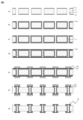
- FIG. 2 is an explanatory diagram showing an example of a method for manufacturing a core substrate according to the present invention.
- FIG. 3 is an explanatory diagram showing a method for manufacturing a wiring board according to the first embodiment of the present invention.
- FIG. 4 is an explanatory diagram showing a method for manufacturing a wiring board according to the first embodiment of the present invention.
- FIG. 5 is an explanatory diagram showing a method for manufacturing a wiring board according to the first embodiment of the present invention.
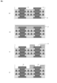
- FIG. 6 is a diagram showing an example of a mounting state.
- FIG. 1 is a diagram showing an example of a cross section of a wiring board for mounting a semiconductor device according to a first embodiment of the present invention.
- FIG. 2 is an explanatory diagram showing an example of a method for manufacturing a core substrate according to the present invention.
- FIG. 3 is an
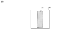
- FIG. 7 is an explanatory diagram showing an example of the second connection terminal region according to the first embodiment of the present invention.
- FIG. 8 is an explanatory diagram showing an example of the second connection terminal region according to the first embodiment of the present invention.
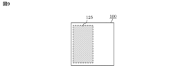
- FIG. 9 is an explanatory diagram showing an example of the second connection terminal region according to the first embodiment of the present invention.
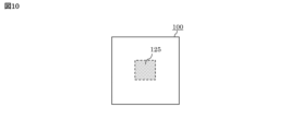
- FIG. 10 is an explanatory diagram showing an example of the second connection terminal region according to the first embodiment of the present invention.
- FIG. 11 is an explanatory diagram showing an example of the second connection terminal region according to the first embodiment of the present invention.
- FIG. 12 is an explanatory diagram showing an example of the second connection terminal region according to the first embodiment of the present invention.
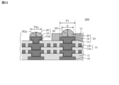
- FIG. 13 is a diagram showing an example of a cross section of a wiring board according to the second embodiment of the present invention.
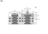
- FIG. 14 is a diagram showing an example of a cross section of a wiring board according to a third embodiment of the present invention.
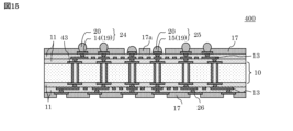
- FIG. 15 is a diagram showing an example of a cross section of a wiring board according to a fourth embodiment of the present invention.
- FIG. 16 is a diagram showing an example of a mounting state.
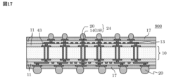
- FIG. 17 is a diagram showing an example of a cross section of a conventional wiring board for mounting a semiconductor device.
- FIG. 18 is an explanatory diagram showing a method for manufacturing a wiring board according to a fifth embodiment of the present invention.
- FIG. 19 is an explanatory diagram showing a method for manufacturing a wiring board according to a fifth embodiment of the present invention.
- FIG. 20 is a diagram showing an example of a mounting state.
- FIG. 21 is an explanatory diagram showing an example of a second connection terminal region according to the fifth embodiment of the present invention.
- FIG. 22 is an explanatory diagram showing an example of a second connection terminal region according to the fifth embodiment of the present invention.
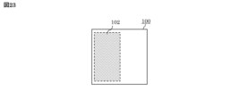
- FIG. 23 is an explanatory diagram showing an example of a second connection terminal region according to the fifth embodiment of the present invention.
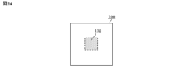
- FIG. 24 is an explanatory diagram showing an example of a second connection terminal region according to the fifth embodiment of the present invention.
- FIG. 25 is an explanatory diagram showing an example of a second connection terminal region according to the fifth embodiment of the present invention.
- FIG. 27 is an explanatory diagram showing an example of a second connection terminal region according to the fifth embodiment of the present invention.
- the wiring board of the present disclosure has a core substrate, and layers having the same function are arranged symmetrically on a first surface and a second surface opposite the first surface.
- the "top surface” of a layer refers to the surface farther from the core substrate
- the “bottom surface” of a layer refers to the surface closer to the core substrate.
- top layer refers to the layer that is in the direction away from the core substrate
- bottom layer refers to the layer that is in the direction closer to the core substrate.
- ⁇ Conventional Example> 17 is a diagram showing an example of a cross section of a conventional wiring board 900 for mounting a semiconductor device.
- the surface on which the first connection terminals 24 are formed is the side on which the semiconductor device is mounted
- the surface on which the solder bumps 20 are formed is the side on which the wiring board 200 is connected to a motherboard or the like.
- the first connection terminals 24 are formed to have a common height. For this reason, when semiconductor devices are mounted one on top of the other, the mounting surface cannot be used efficiently.
- Figure 1 is a diagram showing an example of a cross section of a wiring board for mounting a semiconductor device according to the first embodiment of the present invention.
- the wiring board 100 for mounting a semiconductor device includes a core substrate 10, a plurality of insulating resin layers 11, and a plurality of conductor layers 13.
- the pad portion 43 formed on the core substrate 10 is electrically connected to the conductor layer 13 laminated on the core substrate 10.
- the insulating resin layer 11 is made of a thermosetting resin, a thermoplastic resin, a photosensitive resin, or a resin made by mixing at least two of these, such as an epoxy resin, an acrylic resin, a phenolic resin, a melamine resin, a silicone resin, a polyimide resin, a polyphenylene ether resin, a maleimide resin, a liquid crystal polymer, a fluororesin, or a resin made by combining at least two of these, and may contain an inorganic filler or an organic filler.
- a thermosetting resin such as an epoxy resin, an acrylic resin, a phenolic resin, a melamine resin, a silicone resin, a polyimide resin, a polyphenylene ether resin, a maleimide resin, a liquid crystal polymer, a fluororesin, or a resin made by combining at least two of these, and may contain an inorganic filler or an organic filler.
- the conductor layer 13 has a seed layer 13a and a plating layer 13b in this order from the lower insulating resin layer 11 side.
- a plurality of conductor layers 13 are formed by plating using a resist pattern 16, and etching the seed layer 13a exposed after peeling off the resist pattern 16.
- the conductor layer 13 may include various patterns such as wiring, vias, pads, shields, grounds, and dummies, but wiring, vias, and pads are shown in FIG. 1.
- Adjacent conductor layers 13 are formed spaced apart in the surface direction of the insulating resin layer 11.
- the seed layer 13a is laminated on the insulating resin layer 11.
- the material constituting the seed layer 13a is not particularly limited, but when it is formed by electroless plating, for example, metal materials such as Cu, Pd, Al, Sn, Ni and Cr can be used.
- a material containing at least one of Cu, Ni, Al, Ti, Cr, Mo, W, Ta, Au, Ir, Ru, Pd, Pt, AlSi, AlSiCu, AlCu, NiFe, ITO (indium tin oxide), IZO (indium zinc oxide), AZO (aluminum-doped zinc oxide), ZnO, PZT (lead zirconate titanate), TiN, Cu 3 N 4 , and a Cu alloy can be used.
- the plating layer 13b is laminated on the upper surface of the seed layer 13a.
- the material constituting the plating layer 13b is mainly a metal, and the type is not particularly limited.
- the material constituting the plating layer 13b may be a material containing at least one of Cu and Cu alloys, Ag and Ag alloys, Sn, Pd, Au, Ni, Cr, Pt, and Fe.
- the solder resist layer 17 is made of a thermosetting resin, a thermoplastic resin, a photosensitive resin, or a resin made by mixing at least two of these, such as an epoxy resin, an acrylic resin, a phenol resin, a melamine resin, a silicone resin, a polyimide resin, a polyphenylene ether resin, a maleimide resin, a liquid crystal polymer, a fluororesin, or a resin made by combining at least two of these, and may contain an inorganic filler or an organic filler.
- a thermosetting resin such as an epoxy resin, an acrylic resin, a phenol resin, a melamine resin, a silicone resin, a polyimide resin, a polyphenylene ether resin, a maleimide resin, a liquid crystal polymer, a fluororesin, or a resin made by combining at least two of these, and may contain an inorganic filler or an organic filler.
- the surface on which the first connection terminal 24 and the second connection terminal 25 are formed is connected to, for example, a semiconductor device.
- the first connection terminal 24 is composed of a first connection pad 14 (or a surface treatment layer 19) and a solder bump 20.
- the second connection terminal 25 is composed of a second connection pad 15 (or a surface treatment layer 19) and a solder bump 20.
- the top of the first connection terminal 24 is located farther from the core substrate 10 than the top of the second connection terminal 25.
- the pad portion 26 has a solder bump 20 formed thereon, which is used for connection to a motherboard or the like.
- FIG. 2 is an explanatory diagram showing an example of a method for manufacturing the core board 10 of the present invention.
- through holes 3 for electrically connecting the front and back surfaces are formed by a drill or the like in a core resin 1 having copper foils 2 attached to both sides thereof (FIG. 2(a)).
- a conductor layer 23 is formed on the surface of the copper foil 2 and the wall surface of the through hole 3 by electroless plating and electrolytic plating (FIG. 2(b)).
- electroless plating of the conductor layer 23 a material similar to the material used for the seed layer 13a described below can be used.
- electrolytic plating of the conductor layer 23 a material similar to the material used for the plating layer 13b described below can be used.
- the through-holes 3 are filled with filling resin 4. Any excess filling resin 4 that protrudes from the through-holes 3 is removed by buffing or the like ( Figure 2(c)). Note that if the through-holes 3 are completely filled with plating in the step shown in Figure 2(b), this step is omitted.
- a conductor layer 33 is formed on the entire surface by electroless plating and electrolytic plating (Fig. 2(d)). Note that this step may be omitted if the through-holes 3 are completely filled with plating in the step shown in Fig. 2(b) or if the conductor layer 33 is not required on the hole filling resin.
- a resist is applied or laminated, and a resist pattern 6 is formed by photolithography on the portions of the conductor layers 23 and 33 that are to remain as conductors ( Figure 2(e)). Note that a photosensitive resist is used here.
- the resist pattern 6 is removed to form the core substrate 10 having the pad portion 43 (FIG. 2(g)).
- the pad portion 43 is electrically connected to the conductor layer 13 laminated on the core substrate 10, as described below.
- the manufacturing method for the core substrate 10 has been described above, but this is only one example and other manufacturing methods may also be used.
- FIGS. 3 to 5 are explanatory diagrams showing a method for manufacturing a wiring board according to a first embodiment of the present invention. Note that the illustration of the core resin 1 of the core board 10 is omitted here. Also shown are the wiring layers that are formed on the vertically upward surface of the core board when the core board 10 is placed.
- an insulating resin layer 11 is formed on a core substrate 10, and in the case of a thermosetting resin, a UV or CO2 laser is irradiated to expose a pad portion 43 underneath, and a via opening 8 is formed by photolithography in the case of a photosensitive resin (FIG. 3(a)). Residual resin in the via opening 8 is removed by a desmear solution such as permanganic acid or a dry desmear such as plasma.
- a desmear solution such as permanganic acid or a dry desmear such as plasma.
- a seed layer 13a is formed on the top surface of the insulating resin layer 11, the wall surface of the via opening 8, and the pad portion 43 that corresponds to the bottom surface of the via opening 8 by electroless plating or sputtering ( Figure 3 (b)).
- a resist is applied or laminated on the seed layer 13a, and then exposed and developed to form a resist pattern 16 that corresponds to the pattern of the plating layer 13b ( Figure 3(c)). Note that a photosensitive resist is used here.
- a plating layer 13b is formed by electrolytic plating on the seed layer 13a on which the resist pattern 16 has been formed (FIG. 3(d)).
- the resist pattern 16 is removed (FIG. 3(e)).
- the seed layer 13a (the seed layer 13a that is not covered by the plating layer 13b) that is exposed by removing the resist pattern 16 is removed by etching ( Figure 3(f)).
- the insulating resin layer 11 is laminated so as to cover the conductor layer 13 and the underlying insulating resin layer 11. Note that this step is omitted if a circuit with the desired number of layers has been formed.
- solder resist layer 17 is formed on the outermost layer by coating or laminating ( Figure 4(h)).
- solder resist layer 17 around the second connection pad 15 is removed by photolithography or the like, and an opening 18 is formed in the solder resist layer 17 on the first connection pad 14 (FIG. 4(i)).
- the solder resist layer 17 is, for example, a photosensitive epoxy resin, and may contain an inorganic filler.
- a UV laser or a CO2 laser is irradiated, and the solder resist around the second connection pad 15 is removed by photolithography or the like, and an opening 18 is formed in the solder resist layer 17 on the first connection pad 14.
- the side and part of the top surface of the first connection pad 14 are covered by the solder resist layer 17, and the side and top surface of the second connection pad 15 are not covered by the solder resist layer 17.
- a surface treatment layer 19 is formed on the first connection pad 14 and on the top and side surfaces of the second connection pad 15 within the opening 18 of the solder resist layer ( Figure 4(j)).
- solder bumps 20 are formed on the first connection pads 14 and the second connection pads 15 in the openings 18 of the solder resist layer 17, thereby forming a wiring board 100 for mounting a semiconductor device having a first connection terminal region 124 and a second connection terminal region 125 on the semiconductor device mounting surface (FIG. 5(k)).
- a first connection terminal 24 including a first connection pad 14 and a solder bump 20 is formed
- a second connection terminal 25 including a second connection pad 15 and a solder bump 20 is formed in the second connection terminal region 125.
- first connection terminal 24 is formed according to a first pattern width (pitch), and in the second connection terminal region, at least one second connection terminal is formed according to a second pattern width.
- the first pattern width and the second pattern width can be set to a predetermined length.
- the first pattern width and the second pattern width may be the same length or different lengths.
- the solder bumps 20 can be formed by screen printing when a solder paste is used, or by using solder balls, which are then mounted by ball transfer after screen printing of flux, and melted by reflow.
- solder bumps 20 of the first connection terminals 24 are connected to the surface where the solder resist layer 17 is opened and the first connection pads 14 are exposed, and the solder bumps 20 of the second connection terminals 25 connect to the surface and side of the second connection pads 15. At this time, the solder bumps 20 on the second connection pads 15 spread over the entire top surface or side of the pad, so that the relationship between the height H1 of the solder bumps on the first connection pads 14 and the height H2 of the solder bumps on the second connection pads 15 is H1>H2.
- the pad diameter of the first connection pad 14 is denoted as P1, and the pad diameter of the second connection pad 15 is denoted as P2.
- the pad diameter is not limited to the case where the shape of the connection pad is circular, but is used to indicate the size of the connection pad even when the connection pad has another shape.
- the diameter of the first connection pad 14 (the opening diameter of the solder resist layer 17 on the first connection pad 14) and the diameter of the second connection pad 15 can be made different. With this configuration, it is possible to create a difference between the height H1 of the solder bump on the first connection pad 14 and the height H2 of the solder bump on the second connection pad 15.
- FIG. 6 is a diagram showing an example of the mounting state.
- a state in which a three-dimensional semiconductor element 53 (silicon chip) is mounted on the wiring board 100 is shown.
- This three-dimensional semiconductor element 53 may be a case where a plurality of semiconductor elements are stacked (three-dimensional mounting) or a case where a step exists in the mounting surface of one semiconductor element, and the electrode terminals are electrically connected to the corresponding first connection terminal 24 and second connection terminal 25 on the wiring board 100 via a conductive material such as a solder bump 20 (flip-chip mounting).
- the gap between the mounted three-dimensional semiconductor element 53 and the wiring board 100 is filled with underfill resin 35 such as a thermosetting epoxy resin, and the mechanical joint between the three-dimensional semiconductor element 53 and the wiring board 100 is ensured by heat curing.
- underfill resin 35 such as a thermosetting epoxy resin
- a plurality of unit areas, which are areas on which the three-dimensional semiconductor element 53 is mounted may be formed on the core board 10.
- the wiring board 100 is formed by performing dicing or the like to separate each unit area.
- three-dimensional semiconductor element 53 shows a case where second semiconductor element 52 is mounted on first semiconductor element 51.
- Wiring board 100 is electrically connected to second semiconductor element 52 via first connection terminal 24.
- Wiring board 100 is also electrically connected to first semiconductor element 51 via second connection terminal 25.
- First semiconductor element 51 and second semiconductor element 52 are in direct contact with each other and are electrically connected.
- the three-dimensional semiconductor element 53 is composed of a first semiconductor element 51 and a second semiconductor element 52, and has one step formed in a direction perpendicular to the mounting surface, but there may be at least one step, and there may be two or more steps. That is, the three-dimensional semiconductor element may be one in which two or more types of semiconductor elements are stacked and mounted.
- the step can be formed in the solder resist layer 17 by using a method similar to the method shown in Figures 3 to 5.
- the shape of the solder bumps 20 is described here as being columnar, the shape is not limited to this, and it is also conceivable that the solder bumps may be cylindrical or barrel-shaped after mounting.
- solder bumps 20 used as external connection terminals are formed on the pads 16 exposed from the solder resist layer 17 on the side opposite the mounting surface of the three-dimensional semiconductor element 53.
- the wiring board 100 is mounted on a motherboard or the like via the solder bumps 20.
- FIG. 7 to Fig. 12 show examples of the arrangement of the second connection terminal region 125.
- Fig. 7 to Fig. 12 are explanatory views showing an example of the second connection terminal region according to the first embodiment of the present invention.
- Fig. 7 to Fig. 12 are views of the wiring substrate 100 in a mounted state, as viewed from the semiconductor element mounting surface side.
- FIG. 7 shows a case where the second connection terminal area 125 has a rectangular shape and is located in the center of the wiring board 100.
- the second connection terminal area 125 is formed in the same orientation as two opposing sides of the four sides that form the periphery of the wiring board 100.
- first connection terminal region 124 is included in the areas of the wiring board 100 other than the second connection terminal region 125. The same applies to Figures 8 to 12.
- FIG. 8 shows the case where the second connection terminal area 125 has a shape divided into two areas.
- the divided second connection terminal area 125 has a rectangular shape, and the area of the rectangular portion is equal.
- FIG. 9 shows a case where the second connection terminal area 125 occupies approximately half the area of the wiring board 100.
- FIG. 10 shows a case where the second connection terminal region 125 has a rectangular shape and is formed at a position that overlaps with the center of gravity of the wiring board 100.
- the second connection terminal region 125 has a shape similar to the shape of the wiring board 100.
- FIG. 11 shows a case where the second connection terminal region 125 is formed to surround the region including the first connection terminal region 124.
- FIG. 12 shows a case where the second connection terminal region 125 has a shape divided into two regions.
- the two regions are rectangular in shape and share vertices of the rectangle.
- the second connection terminal region 125 shown in the figure is just one example, and various other regions may be used depending on the size and shape of the three-dimensional semiconductor element 53.
- the shape of the wiring board 100 is a square, the present invention is also applicable to cases where the wiring board 100 has a shape other than a square.
- the arrangement of the first connection terminal region 124 and the second connection terminal region 125 may be interchanged.
- Example 1 In Example 1, an example in which the first connection terminal 24 and the second connection terminal 25 of the first embodiment are formed will be described.
- an interlayer insulating resin manufactured by Ajinomoto Co., Inc.
- a copper-clad laminate manufactured by Showa Denko Materials Co., Ltd.
- desmearing was performed using permanganic acid without forming via holes.
- an electroless copper plating layer was formed on the desmeared interlayer insulating resin.
- a dry film resist Showa Denko Materials
- the dry film resist was peeled off, and the electroless copper plating layer not covered by the electrolytic copper plating was etched to form connection pads with a diameter of approximately 180 ⁇ m.
- the copper surface is roughened using a roughening liquid (manufactured by MEC).
- a dry film solder resist manufactured by Showa Denko Materials
- a direct imaging exposure machine and spray developed. This forms an opening in the solder resist layer at the first connection pad area, and removes the solder resist at the second connection pad area.
- the opening in the solder resist layer at this time is formed with a diameter of approximately 80 ⁇ m at the bottom.
- solder balls manufactured by Senju Metal Industry Co., Ltd.
- the diameter of the solder balls used is, for example, 70 ⁇ m.
- the difference in height between the completed first and second connection terminals was measured using a laser interferometer, and the largest difference between the first and second connection terminals was approximately 25 ⁇ m.
- the wiring board 100 By configuring the wiring board 100 so that the height of the first connection terminal 24 in the first connection terminal region 124 is higher than the height of the terminal of the second connection terminal 25 in the second connection terminal region 125, when mounting a semiconductor device on the wiring board 100, it becomes possible to mount a semiconductor device in the second connection terminal region 125 and then mount another semiconductor device on the semiconductor device.
- the wiring board for mounting a semiconductor device according to the present disclosure makes it possible to increase the degree of freedom in designing a three-dimensional stacked structure.
- the second embodiment differs from the first embodiment in that the pad diameter of the second connection pad 15 is changed.
- the same or equivalent components as those in the first embodiment described above are denoted by the same reference numerals, and the description thereof will be simplified or omitted.
- FIG. 13 is a diagram showing an example of a cross section of a wiring board 200 according to a second embodiment of the present invention.
- the pad diameter P2a of the second connection pad 15a is formed to be smaller than the pad diameter P2 of the second connection pad 15 in the first embodiment.
- the solder bump 20 is formed by screen printing or a method using solder balls, and the amount of solder used per second connection pad 15a is not changed. Therefore, the height H2a of the solder bump 20 of the second connection pad 15a is greater than the height H2 of the solder bump 20 of the second connection pad 15 in the first embodiment.
- the pad diameter P2a of the second connection pad 15a is made small
- the pad diameter may be made large.
- the height of the solder bump 20 of the second connection pad 15a will be smaller than the height H2 of the judgment bump of the second connection pad in the first embodiment.
- the third embodiment differs from the first embodiment in that the opening diameter of the solder resist layer 17 on the first connection pad is changed.
- the same or equivalent components as those in the first embodiment described above are denoted by the same reference numerals, and the description thereof will be simplified or omitted.
- FIG. 14 is a diagram showing an example of a cross section of a wiring board 300 according to a third embodiment of the present invention.
- the opening diameter S of the first connection pad 14 is smaller than that in the first embodiment. This is because the opening 18a formed in the solder resist layer 17 is made smaller. Therefore, the size of the surface treatment layer 19 on the first connection pad 14 also changes according to the size of the opening 18a.
- the solder bump 20 is formed by screen printing or a method using solder balls, but the amount of solder used per first connection pad 14 is not changed. Therefore, the height H1a of the solder bump 20 of the first connection pad 14 is greater than the height H1 of the solder bump 20 of the first connection pad 14 in the first embodiment.
- the opening diameter S of the opening 18a in the solder resist layer 17 is made small
- the opening diameter S may be made large.
- the height of the solder bump 20 of the first connection pad 14 will be smaller than the height H1 of the judgment bump of the first connection pad 14 in the first embodiment.
- the opening diameter S of the opening 18a of the solder resist layer 17 on the first connection pad 14 it is possible to control the height H1a of the solder bump on the first connection pad 14.
- the height gap adjustment between the solder bump 20 of the first connection terminal 24 and the solder bump 20 of the second connection terminal 25 can be controlled by the size of the opening diameter of the solder resist layer 17 on the first connection pad 14.
- the wiring board for mounting a semiconductor device of the present disclosure makes it possible to further increase the degree of freedom in designing a three-dimensional stacked structure.
- the fourth embodiment differs from the first embodiment in that the shape of the solder resist layer 17 is changed.
- the same or equivalent components as those in the first embodiment described above are denoted by the same reference numerals, and the description thereof will be simplified or omitted.
- FIG. 15 is a diagram showing an example of a cross section of a wiring board 300 according to a fourth embodiment of the present invention.
- the solder resist layer 17 was not formed between the second connection pads 15, but here, the solder resist layer 17a is left between the second connection pads 15 without being removed.
- FIG. 16 shows an example of the mounting state.
- the second connection terminals 25 around the solder resist layer 17a electrically connect the first semiconductor element 51 and the wiring board 400.
- solder resist layer 17a By leaving the solder resist layer 17a between the second connection pads 15, it is possible to suppress the occurrence of a so-called solder bridge, in which the solder bumps 20 on the second connection pads 15 are connected to each other. In this way, since the solder resist layer can be formed between the solder bumps depending on, for example, the conditions of the semiconductor device to be mounted, the wiring board for mounting a semiconductor device according to the present disclosure allows for greater freedom in designing a three-dimensional stacked structure.
- the fifth embodiment differs from the first embodiment in that both the first connection pad 14 and the second connection pad 15 are covered with a solder resist layer.
- the same or equivalent components as those in the first embodiment described above are denoted by the same reference numerals, and the description thereof will be simplified or omitted.
- FIGS. 18 to 20 are explanatory diagrams showing a method for manufacturing a wiring board according to a fifth embodiment of the present invention. Note that in FIG. 18 and FIG. 19, the core resin 1 of the core board 10 is omitted. Also shown is the wiring layer that is formed on the vertically upward surface of the core board when the core board 10 is placed.
- the manufacturing method of the core substrate 10 can be the manufacturing method in the first embodiment described with reference to FIG. 2. Also, the wiring layer can be formed by the formation method in the embodiment of the base 1 described with reference to FIG. 3.
- FIG. 18(g) shows the state where the wiring layers are repeatedly formed and the circuit with the desired number of layers is formed. Also, FIG. 4(h) shows the state where the solder resist layer 17 is formed on the outermost layer by coating or lamination after the circuit with the desired number of layers is formed.
- the solder resist layer 17 is partially removed by photolithography or the like to form an opening 18 in the solder resist layer 17 (FIG. 18(i)).
- the solder resist layer 17 is, for example, a photosensitive epoxy resin, and may contain an inorganic filler.
- a UV laser or a CO2 laser is irradiated, and the opening 18 is formed in the solder resist layer 17 by photolithography or the like.
- the opening diameter of the opening 18 in the solder resist layer 17 in the first connection terminal region 101 may be smaller than the opening diameter of the opening 18 in the solder resist layer 17 in the second connection terminal region 102.
- the opening diameter of the opening 18 in the first connection terminal region 101 and the opening diameter of the opening 18 in the second connection terminal region 102 can be appropriately selected.
- a surface treatment layer 19 is formed on the first connection pad 14 and the second connection pad 15 within the opening 18 of the solder resist layer 17 ( Figure 18 (j)).
- solder bump 20 is formed on the first connection pad 14 in the opening 18 of the solder resist layer 17 to form a first connection terminal region 101 (FIG. 19(k)). If a solder paste is used, the solder bump 20 can be formed by screen printing. If a solder ball is used, the solder ball is placed by ball transfer after screen printing of flux, and then melted by reflow. Also, the second connection pad 15 is covered with an arbitrary resist to prevent a solder bump from being formed, and is peeled off after the solder bump is formed on the first connection pad 14.
- solder resist layer 17a and an opening 18a in the solder resist layer 17a are formed (FIG. 19(m)).
- the solder resist layer 17 in the first connection terminal region 101 is thinner than the solder resist layer (solder resist layer 17 and solder resist layer 17a) in the second connection terminal region 102.
- the solder resist layer (solder resist layer 17 and solder resist layer 17a) in the second connection terminal region 102 is obtained by stacking at least two or more solder resist layers, and the number of layers is greater than the number of layers of the solder resist layer 17 in the first connection terminal region 101.
- the second connection terminal region 102 is formed by forming a solder bump 20 on the second connection pad 15 (FIG. 19(n)).
- a wiring board 100 for mounting a semiconductor device having the first connection terminal region 101 and the second connection terminal region 102 on the semiconductor device mounting surface can be formed.
- the solder resist layer 17 and the solder bumps 20 for the first connection terminal region 101 are formed on the front surface of the outermost surface of the board before the solder resist layer 17a is formed, and then a new solder resist layer 17a and a solder bump 20 are formed only in the second connection terminal region 102 to form the second connection terminal region 102.
- the first connection terminal region 101 and the second connection terminal region 102 are regions having a solder resist layer and a solder bump.
- FIG. 20 is a diagram showing an example of the mounting state.
- a semiconductor device is shown in which a three-dimensional semiconductor element having at least two or more thicknesses is mounted on a wiring board 100.
- a state in which a three-dimensional semiconductor element 53 (silicon chip) is mounted on the wiring board 100 is shown.
- This three-dimensional semiconductor element 53 may be a case in which multiple semiconductor elements are stacked (three-dimensional mounting) or a case in which a step exists in the mounting surface of one semiconductor element, and the electrode terminals are electrically connected to the corresponding first connection terminal 24 and second connection terminal 25 on the wiring board 100 via a conductive material such as a solder bump 20 (flip-chip mounting).
- the gap between the mounted three-dimensional semiconductor element 53 and the wiring board 100 is filled with underfill resin 35 such as a thermosetting epoxy resin, and the mechanical joint between the three-dimensional semiconductor element 53 and the wiring board 100 is ensured by heat curing.
- underfill resin 35 such as a thermosetting epoxy resin
- a plurality of unit areas which are areas in which the three-dimensional semiconductor element 53 is mounted, may be formed on the core board 10.
- the wiring substrate 100 is formed by dividing into individual unit areas.
- the height of the solder bump and the thickness of the solder resist layer are different, as shown in the first connection terminal 24 and the second connection terminal 25.
- the solder bump 20 in the first connection terminal region 101 is shorter in height than the solder bump 20 in the second connection terminal region 102.
- three-dimensional semiconductor element 53 shows a case where second semiconductor element 52 is mounted on first semiconductor element 51.
- Wiring board 100 is electrically connected to second semiconductor element 52 via first connection terminal 24.
- Wiring board 100 is also electrically connected to first semiconductor element 51 via second connection terminal 25.
- First semiconductor element 51 and second semiconductor element 52 are in direct contact with each other and are electrically connected.
- the three-dimensional semiconductor element 53 is composed of a first semiconductor element 51 and a second semiconductor element 52, and has one step formed in the direction perpendicular to the mounting surface, but the step may be two or more steps. In other words, the three-dimensional semiconductor element may be one in which two or more types of semiconductor elements are stacked and mounted.
- the shape of the solder bumps 20 is described here as being columnar, the shape is not limited to this, and it is also conceivable that the solder bumps may be cylindrical or barrel-shaped after mounting. Further, although the case is shown in which the thickness of the first semiconductor element 51 is different from the thickness of the second semiconductor element 52, the thicknesses of the first semiconductor element 51 and the second semiconductor element 52 can be set as appropriate.
- solder bumps 20 used as external connection terminals are formed on the pads 16 exposed from the solder resist layer 17 on the side opposite the mounting surface of the three-dimensional semiconductor element 53.
- the wiring board 100 is mounted on a motherboard or the like via the solder bumps 20.
- FIG. 21 to 26 show examples of the arrangement of the second connection terminal region 102.
- Fig. 21 to Fig. 26 are explanatory views showing an example of the second connection terminal region according to the fifth embodiment of the present invention.
- Fig. 21 to Fig. 26 are views of the wiring substrate 100 in a mounted state, as viewed from the semiconductor element mounting surface side.
- FIG. 21 shows a case where the second connection terminal area 102 has a rectangular shape and is arranged in the center of the wiring board 100.
- the second connection terminal area 102 is formed in the same orientation as two opposing sides of the four sides that form the periphery of the wiring board 100.
- first connection terminal region 101 is included in the areas of the wiring board 100 other than the second connection terminal region 102.
- FIG. 22 shows a case where the second connection terminal area 102 has a shape divided into two areas.
- the divided second connection terminal area 102 has a rectangular shape, and the area of the rectangular portion is equal.
- FIG. 23 shows a case where the second connection terminal area 102 occupies approximately half the area of the wiring board 100.
- FIG. 24 shows a case where the second connection terminal region 102 has a rectangular shape and is formed at a position that overlaps with the center of gravity of the wiring board 100.
- the second connection terminal region 102 has a shape similar to the shape of the wiring board 100.
- FIG. 25 shows a case where the second connection terminal region 102 is formed to surround the region including the first connection terminal region 101.
- FIG. 26 shows a case where the second connection terminal region 102 has a shape divided into two regions.
- the two regions are rectangular in shape and share vertices of the rectangle.
- the second connection terminal region 102 shown in the figure is an example, and various other regions can be used depending on the size and shape of the three-dimensional semiconductor element 53.
- the shape of the wiring board 100 is a square, but the wiring board 100 can also be applied to cases where the wiring board 100 has a shape other than a square.
- the arrangement of the first connection terminal region 101 and the second connection terminal region 102 may be interchanged.
- the connection terminal region on the inside when viewed from above is the first connection terminal region 101
- the connection terminal region on the outside when viewed from above is the second connection terminal region 102, but it is also possible for the outside to be the first connection terminal region 101 and the inside to be the second connection terminal region 102.
- Example 2 In Example 2, an example in which the first connection terminal 24 and the second connection terminal 25 of the fifth embodiment are formed will be described.
- an interlayer insulating resin manufactured by Ajinomoto Co., Inc.
- a copper-clad laminate manufactured by Showa Denko Materials Co., Ltd.
- desmearing was performed using permanganic acid without forming via holes.
- an electroless copper plating layer was formed on the desmeared interlayer insulating resin.
- a dry film resist Showa Denko Materials
- the dry film resist was peeled off, and the electroless copper plating layer not covered by the electrolytic copper plating was etched to form connection pads with a diameter of approximately 180 ⁇ m.
- the copper surface is roughened using a roughening liquid (manufactured by MEC).
- a dry film solder resist manufactured by Showa Denko Materials
- a direct imaging exposure machine and spray developed. This forms an opening in the solder resist layer at the first connection pad area, and removes the solder resist at the second connection pad area.
- the opening in the solder resist layer at this time is formed with a diameter of approximately 80 ⁇ m at the bottom.
- solder balls manufactured by Senju Metal Industry Co., Ltd.
- the diameter of the solder balls used is, for example, 70 ⁇ m.
- the difference in height between the completed first and second connection terminals was measured using a laser interferometer, and the largest difference between the first and second connection terminals was approximately 25 ⁇ m.
- the wiring board 100 By configuring the wiring board 100 so that the height of the second connection terminal 25 in the second connection terminal region 102 is higher than the height of the terminal of the first connection terminal 24 in the first connection terminal region 101, when mounting a semiconductor device on the wiring board 100, it becomes possible to mount a semiconductor device in the first connection terminal region 101 and then mount another semiconductor device on the semiconductor device.
- the wiring board for mounting a semiconductor device according to the present disclosure makes it possible to increase the degree of freedom in designing a three-dimensional stacked structure.
- the solder resist layer also has the effect of preventing solder from adhering to unnecessary areas. Because the solder resist layer is provided between the first connection terminal 24 and the second connection terminal 25, the distance between the connection terminals can be made smaller than when there is no solder resist layer, making it possible to realize a pattern of connection terminals with a narrow pitch. For example, when there is a solder resist layer, the width between the connection terminals can be set to a value of 45 ⁇ m to 50 ⁇ m. On the other hand, when there is no solder resist layer, the width between the connection terminals is approximately 100 ⁇ m.
- a wiring board for mounting a semiconductor device A semiconductor device mounting surface has a first connection terminal area and a second connection terminal area, A first connection terminal including a first connection pad and a solder bump is formed in the first connection terminal region;
- a wiring board for mounting a semiconductor device characterized in that a second connection terminal including a second connection pad and a solder bump is formed in the second connection terminal area, a side surface and a portion of an upper surface of the first connection pad are covered by a solder resist layer, and a side surface and an upper surface of the second connection pad are not covered by the solder resist layer.
- Aspect 5 The wiring board for mounting a semiconductor device according to claim 1, wherein a diameter of an opening in the solder resist layer on the first connection pad and a diameter of the second connection pad are different in size.
- the method for manufacturing a wiring substrate for mounting a semiconductor device according to the first aspect is characterized in that the height gap between the solder bump of the first connection terminal and the solder bump of the second connection terminal is adjusted by controlling the diameter of the second connection pad.
- a wiring board for mounting a semiconductor device A semiconductor device mounting surface has a first connection terminal area and a second connection terminal area, the first connection terminal region and the second connection terminal region are regions having a solder resist layer and a solder bump, a height of the solder bump and a thickness of the solder resist layer in the first connection terminal region and the second connection terminal region, the height of the solder bump and the thickness of the solder resist layer being different from each other.
- Aspect 10 10. The wiring board according to claim 9, wherein the solder bumps in the first connection terminal region are lower in height than the solder bumps in the second connection terminal region.
- a semiconductor device comprising the wiring board according to any one of aspects 9 to 14, and a three-dimensional semiconductor element having at least two thicknesses mounted on the wiring board.
Landscapes
- Engineering & Computer Science (AREA)
- Manufacturing & Machinery (AREA)
- Microelectronics & Electronic Packaging (AREA)
- Electric Connection Of Electric Components To Printed Circuits (AREA)
- Physics & Mathematics (AREA)
- Geometry (AREA)
- Production Of Multi-Layered Print Wiring Board (AREA)
Abstract
Description
また、特許文献2は、配線基板1と半導体装置2、または2つの半導体装置2に挟まれた半導体装置2の配線基板1側の面とその反対側の面との双方にバンプ接続用電極3を有し、そのうち一方の面に形成された一部又は全部のバンプ接続用電極3がもう一方の面に設けられたバンプ接続用電極3に電気的に接続されることを開示する。
上記した以外の課題、構成および効果は、以下の実施をするための形態における説明により明らかにされる。
図17は、従来の半導体装置実装用の配線基板900の断面の一例を示す図である。ここで、第一接続端子24が形成された面は半導体装置が実装される側であり、はんだバンプ20が形成された面は配線基板200がマザーボード等に接続される側である。半導体装置が実装される側の面において、第一接続端子24は共通の高さを持つように形成されている。このため、半導体装置を重ねて実装する場合、実装面を効率的に用いることができない。
図1~図12を参照して第1の実施形態について説明する。図1は、本発明の第1の実施形態に係る半導体装置実装用の配線基板の断面の一例を示す図である。
半導体装置実装用の配線基板100は、コア基板10と複数の絶縁樹脂層11と、複数の導体層13とを備える。コア基板10上に形成されたパッド部43は、コア基板10に積層される導体層13と電気的に接続される。
絶縁樹脂層11は、熱硬化性樹脂、熱可塑性樹脂、感光性樹脂またはこれらのうち少なくとも2つを混合した樹脂から構成される。例えば、エポキシ樹脂、アクリル樹脂、フェノール樹脂、メラミン樹脂、シリコーン樹脂、ポリイミド樹脂、ポリフェニレンエーテル樹脂、マレイミド樹脂、液晶ポリマー、フッ素樹脂、またはこれらのうちの少なくとも2つを組み合わせた樹脂であり、無機フィラーまたは有機フィラーを含有しても良い。
導体層13は、後述するように、下層の絶縁樹脂層11側から順に、シード層13aおよびめっき層13bを有する。レジストパターン16を用いてめっきし、レジストパターン16を剥離後に剥き出しとなったシード層13aをエッチングすることにより、複数の導体層13が形成される。導体層13には、配線、ビア、パッド、シールド、グランド、ダミーなどの様々なパターンが含まれ得るが、図1においては配線、ビア、パッド部を示す。隣接する導体層13は絶縁樹脂層11の面方向に離間して形成されている。
シード層13aは、絶縁樹脂層11上に積層される。シード層13aを構成する材料は特に制限されないが、無電解めっき法で形成する場合、例えば、Cu、Pd、Al、Sn、NiおよびCrなどの金属材料を用いることができる。スパッタリング法で形成する場合、例えば、Cu、Ni、Al、Ti、Cr、Mo、W、Ta、Au、Ir、Ru、Pd、Pt、AlSi、AlSiCu、AlCu、NiFe、ITO(Indium Tin Oxide)、IZO(Indium Zinc Oxide)、AZO(Aluminum-doped Zinc Oxide)、ZnO、PZT(チタン酸ジルコン酸鉛)、TiN、Cu3N4、Cu合金のうちの少なくとも1つを含む材料を用いることができる。
めっき層13bは、シード層13aの上面に積層される。めっき層13bを構成する材料は、主に金属であり、種類は特に制限されない。めっき層13bを構成する材料は、例えば、CuおよびCu合金、AgおよびAg合金、Sn、Pd、Au、Ni、Cr、Pt、Feのうち少なくとも1つ含む材料を用いることができる。
ソルダーレジスト層17は、熱硬化性樹脂、熱可塑性樹脂、感光性樹脂またはこれらのうちの少なくとも2つを混合した樹脂から構成される。例えば、エポキシ樹脂、アクリル樹脂、フェノール樹脂、メラミン樹脂、シリコーン樹脂、ポリイミド樹脂、ポリフェニレンエーテル樹脂、マレイミド樹脂、液晶ポリマー、フッ素樹脂、またはこれらのうちの少なくとも2つを組み合わせた樹脂であり、無機フィラーまたは有機フィラーを含有しても良い。
第一接続端子24および第二接続端子25が形成された面は、例えば、半導体装置が接続される。第一接続端子24は、第一接続パッド14(または表面処理層19)とはんだバンプ20によって構成される。第二接続端子25は、第二接続パッド15(または表面処理層19)とはんだバンプ20によって構成される。ここで示されるように、第一接続端子24の頂部のほうが、第二接続端子25の頂部よりも、コア基板10から離れた位置にある。
また、パッド部26は、はんだバンプ20が形成され、マザーボード等との接続に用いられる。
第1の実施形態に係る配線基板100の製造方法を説明する。まず、図2を参照しながら、コア基板10を製造する工程を説明する。図2は、本発明のコア基板10の製造方法の一例を示す説明図である。
まず、両面に銅箔2が貼付されたコア樹脂1に、ドリル等で表裏面を電気的に接続するためのスルーホール3を形成する(図2(a))。
次に、製造したコア基板10に絶縁樹脂層と導体片が形成された層(導体層13)を複数積層し、配線基板100を作製(製造)する工程を説明する。なお、絶縁樹脂層と導体層は、コア基板10の両面に積層される。
次に、レジストパターン16を除去する(図3(e))。
なお、3次元半導体素子53は、第一半導体素子51と第二半導体素子52によって構成され、実装面に垂直な方向に対して段差が1段形成されているが、段差は少なくとも1つあればよく、2段以上であってもよい。すなわち、3次元半導体素子は、2種類以上の半導体素子を重ねて実装したものであってもよい。例えば、段差は、ソルダーレジスト層17において図3から図5に示す方法と同様の方法を用いることによって形成することが可能である。
また、ここでははんだバンプ20の形状を柱状に記載しているが、形状はこれに限定されるものではない。実装後には円柱または樽状になる場合も考えられる。
第二接続端子領域125の配置の例を図7~図12に示す。図7~図12は、本発明の第1の実施形態に係る第二接続端子領域の一例を示す説明図である。図7~図12は、実装状態において、配線基板100を半導体素子実装面側から見た図である。
2つの領域は矩形の形状であり、矩形の頂点を共有している。
実施例1では第1の実施形態の第一接続端子24および第二接続端子25を形成した例について説明する。
第一接続端子領域124における第一接続端子24の高さを第二接続端子領域125における第二接続端子25の端子の高さよりも高くした配線基板100とすることによって、半導体装置を配線基板100に実装する場合、第二接続端子領域125に半導体装置を搭載したうえで、さらに、その半導体装置上に別の半導体装置を実装することが可能になる。このように、本開示の半導体装置実装用の配線基板によれば、3次元積層構造の設計自由度を高めることが可能となる。
第2の実施形態は、第二接続パッド15のパッド径を変更した点で、第1の実施形態と異なる。以下の説明において、上述の第1の実施形態と同一または同等の構成要素については同一の符号を付し、その説明を簡略または省略する。
このように、第一接続パッド14および第二接続パッド15を形成する際に、第二接続パッド15のパッド径P2を調整することで、後のはんだバンプ20の濡れ広がり幅が変わり、第二接続パッド上のはんだバンプ高さを制御することができる。言い換えると、第一接続端子24のはんだバンプ20と、第二接続端子25のはんだバンプ20の高さギャップ調整は、第二接続パッド15の径の大きさで制御することができる。このように、はんだバンプの高さの変更を、例えば実装する半導体装置の条件に応じて行うことができるため、本開示の半導体装置実装用の配線基板によれば、3次元積層構造の設計自由度をより高めることが可能となる。
第3の実施形態は、第一接続パッド上のソルダーレジスト層17の開口径を変更した点で、第1の実施形態と異なる。以下の説明において、上述の第1の実施形態と同一または同等の構成要素については同一の符号を付し、その説明を簡略または省略する。
このように、第一接続パッド14上の、ソルダーレジスト層17の開口部18aの開口径Sを調整することによって、第一接続パッド14上のはんだバンプの高さH1aを制御することができる。言い換えると、第一接続端子24のはんだバンプ20と、第二接続端子25のはんだバンプ20の間における高さのギャップ調整は、第一接続パッド14上のソルダーレジスト層17の開口径の大きさで制御することができる。このように、はんだバンプの高さの変更を、例えば実装する半導体装置の条件に応じて行うことができるため、本開示の半導体装置実装用の配線基板によれば、3次元積層構造の設計自由度をより高めることが可能となる。
第4の実施形態は、ソルダーレジスト層17の形状を変更した点で、第1の実施形態と異なる。以下の説明において、上述の第1の実施形態と同一または同等の構成要素については同一の符号を付し、その説明を簡略または省略する。
第二接続パッド15の間にソルダーレジスト層17aを残すことによって、第二接続パッド15上のはんだバンプ20同士が接続してしまう、いわゆるはんだブリッジの発生を抑制することができる。このように、例えば実装する半導体装置の条件に応じて、はんだバンプの間にソルダーレジスト層を形成することができるため、本開示の半導体装置実装用の配線基板によれば、3次元積層構造の設計自由度をより高めることが可能となる。
第5の実施形態は、第一接続パッド14と第二接続パッド15のいずれもソルダーレジスト層で覆われる点で、第1の実施形態と異なる。以下の説明において、上述の第1の実施形態と同一または同等の構成要素については同一の符号を付し、その説明を簡略または省略する。
なお、3次元半導体素子53は、第一半導体素子51と第二半導体素子52によって構成され、実装面に垂直な方向に対して段差が1段形成されているが、段差は2段以上であってもよい。すなわち、3次元半導体素子は、2種類以上の半導体素子を重ねて実装したものであってもよい。
また、ここでははんだバンプ20の形状を柱状に記載しているが、形状はこれに限定されるものではない。実装後には円柱または樽状になる場合も考えられる。
また、第一半導体素子51の厚みは第二半導体素子52の厚みとは異なる場合が示されているが、第一半導体素子51の厚みと第二半導体素子52の厚みは適宜設定しうる。
第二接続端子領域102の配置の例を図21~図26に示す。図21~図26は、本発明の第5の実施形態に係る第二接続端子領域の一例を示す説明図である。図21~図26は、実装状態において、配線基板100を半導体素子実装面側から見た図である。
実施例2では第5の実施形態の第一接続端子24および第二接続端子25を形成した例について説明する。
第二接続端子領域102における第二接続端子25の高さを第一接続端子領域101における第一接続端子24の端子の高さよりも高くした配線基板100とすることによって、半導体装置を配線基板100に実装する場合、第一接続端子領域101に半導体装置を搭載したうえで、さらに、その半導体装置上に別の半導体装置を実装することが可能になる。このように、本開示の半導体装置実装用の配線基板によれば、3次元積層構造の設計自由度を高めることが可能となる。
本開示は、次の態様も含む。
(態様1)
半導体装置実装用の配線基板であって、
半導体装置実装面において、第一接続端子領域と、第二接続端子領域を有し、
前記第一接続端子領域には、第一接続パッドとはんだバンプを含む第一接続端子が形成され、
前記第二接続端子領域には、第二接続パッドとはんだバンプを含む第二接続端子が形成され
前記第一接続パッドの側面と上面の一部はソルダーレジスト層によって覆われており、前記第二接続パッドの側面および上面はソルダーレジスト層によって覆われていない、ことを特徴とする半導体装置実装用の配線基板。
(態様2)
前記半導体装置実装面において、前記第一接続端子のはんだバンプの高さは、前記第二接続端子のはんだバンプよりも高さよりも高いことを特徴とする態様1に記載の半導体装置実装用の配線基板。
(態様3)
前記第一接続端子のはんだバンプは、前記ソルダーレジスト層が開口し前記第一接続パッドが露出する表面と接続されており、
前記第二接続端子のはんだバンプは、前記第二接続パッドの表面および側面とを接続すること特徴とする態様1または2に記載の半導体装置実装用の配線基板。
(態様4)
前記半導体装置実装面に垂直な方向から見た場合、前記第一接続パッドの径と、前記第二接続パッドの径は異なることを特徴とする態様1から態様3のいずれか1つに記載の半導体装置実装用の配線基板。
(態様5)
前記第一接続パッド上のソルダーレジスト層の開口径と前記第二接続パッドの径は、大きさが異なる態様1から態様4のいずれか1つに記載の半導体装置実装用の配線基板。
(態様6)
少なくとも1つの段差を有する3次元半導体素子が実装されることを特徴とする態様1から態様5のいずれか1つに記載の半導体装置実装用の配線基板。
(態様7)
前記第一接続端子のはんだバンプと、前記第二接続端子のはんだバンプの高さギャップ調整は、前記第一接続パッド上のソルダーレジスト開口径の大きさで制御することを特徴とする態様1に記載の半導体装置実装用の配線基板の製造方法。
(態様8)
前記第一接続端子のはんだバンプと、前記第二接続端子のはんだバンプの高さギャップ調整は、前記第二接続パッドの径の大きさで制御することを特徴とする態様1に記載の半導体装置実装用の配線基板の製造方法。(態様9)
半導体装置実装用の配線基板であって、
半導体装置実装面において、第一接続端子領域と、第二接続端子領域を有し、
前記第一接続端子領域および前記第二接続端子領域は、ソルダーレジスト層および半田バンプを有する領域であり、
前記第一接続端子領域と前記第二接続端子領域において、はんだバンプの高さ、およびソルダーレジスト層の厚みがそれぞれ異なることを特徴とする配線基板。
(態様10)
前記第一接続端子領域のはんだバンプは、前記第二接続端子領域のはんだバンプよりも高さが低いことを特徴とする態様9に記載の配線基板。
(態様11)
前記第一接続端子領域のソルダーレジスト層の開口径は、前記第二接続端子領域のソルダーレジスト層の開口径よりも小さいことを特徴とする態様9または態様10に記載の配線基板。
(態様12)
前記第一接続端子領域のソルダーレジスト層は、前記第二接続端子領域のソルダーレジスト層よりも薄いことを特徴とする態様9から態様11のいずれか1つに記載の配線基板。
(態様13)
前記第二接続端子領域のソルダーレジスト層は、少なくとも2層以上のソルダーレジスト層を積層して得られ、かつ前記第一接続端子領域のソルダーレジスト層の積層数よりも多いことを特徴とする態様9から態様12のいずれか1つに記載の配線基板。
(態様14)
上面視にて内側にある接続端子領域を前記第一接続端子領域とし、上面視にて外側にある接続端子領域を前記第二接続端子領域とすることを特徴とする態様9から態様13のいずれか1つに記載の配線基板。
(態様15)
態様9から態様14のいずれか1つに記載の前記配線基板に、少なくとも2つ以上の厚みを有する3次元半導体素子を実装してなる半導体装置。
(態様16)
態様9から態様15のいずれか1つに記載の配線基板の製造方法であって、
前記配線基板の製造において、ソルダーレジスト層形成前の基板最外面の前面に第一接続端子領域用のソルダーレジスト層とはんだバンプを形成した後に、前記第二接続端子領域のみ新たなソルダーレジスト層とはんだバンプを形成して前記第二接続端子領域を形成する製造方法。
Claims (16)
- 半導体装置実装用の配線基板であって、
半導体装置実装面において、第一接続端子領域と、第二接続端子領域を有し、
前記第一接続端子領域には、第一接続パッドとはんだバンプを含む第一接続端子が形成され、
前記第二接続端子領域には、第二接続パッドとはんだバンプを含む第二接続端子が形成され
前記第一接続パッドの側面と上面の一部はソルダーレジスト層によって覆われており、前記第二接続パッドの側面および上面はソルダーレジスト層によって覆われていない、ことを特徴とする半導体装置実装用の配線基板。 - 前記半導体装置実装面において、前記第一接続端子のはんだバンプの高さは、前記第二接続端子のはんだバンプよりも高さよりも高いことを特徴とする請求項1に記載の半導体装置実装用の配線基板。
- 前記第一接続端子のはんだバンプは、前記ソルダーレジスト層が開口し前記第一接続パッドが露出する表面と接続されており、
前記第二接続端子のはんだバンプは、前記第二接続パッドの表面および側面とを接続すること特徴とする請求項1記載の半導体装置実装用の配線基板。 - 前記半導体装置実装面に垂直な方向から見た場合、前記第一接続パッドの径と、前記第二接続パッドの径は異なることを特徴とする請求項1に記載の半導体装置実装用の配線基板。
- 前記第一接続パッド上のソルダーレジスト層の開口径と前記第二接続パッドの径は、大きさが異なる請求項1に記載の半導体装置実装用の配線基板。
- 少なくとも1つの段差を有する3次元積層半導体素子が実装されることを特徴とする請求項1から請求項5のいずれか1項に記載の半導体装置実装用の配線基板。
- 前記第一接続端子のはんだバンプと、前記第二接続端子のはんだバンプの高さギャップ調整は、前記第一接続パッド上のソルダーレジスト開口径の大きさで制御することを特徴とする請求項1に記載の半導体装置実装用の配線基板の製造方法。
- 前記第一接続端子のはんだバンプと、前記第二接続端子のはんだバンプの高さギャップ調整は、前記第二接続パッドの径の大きさで制御することを特徴とする請求項1に記載の半導体装置実装用の配線基板の製造方法。
- 半導体装置実装用の配線基板であって、
半導体装置実装面において、第一接続端子領域と、第二接続端子領域を有し、
前記第一接続端子領域および前記第二接続端子領域は、ソルダーレジスト層および半田バンプを有する領域であり、
前記第一接続端子領域と前記第二接続端子領域において、はんだバンプの高さ、およびソルダーレジスト層の厚みがそれぞれ異なることを特徴とする配線基板。 - 前記第一接続端子領域のはんだバンプは、前記第二接続端子領域のはんだバンプよりも高さが低いことを特徴とする請求項9に記載の配線基板。
- 前記第一接続端子領域のソルダーレジスト層の開口径は、前記第二接続端子領域のソルダーレジスト層の開口径よりも小さいことを特徴とする請求項9に記載の配線基板。
- 前記第一接続端子領域のソルダーレジスト層は、前記第二接続端子領域のソルダーレジスト層よりも薄いことを特徴とする請求項9に記載の配線基板。
- 前記第二接続端子領域のソルダーレジスト層は、少なくとも2層以上のソルダーレジスト層を積層して得られ、かつ前記第一接続端子領域のソルダーレジスト層の積層数よりも多いことを特徴とする請求項12に記載の配線基板。
- 上面視にて内側にある接続端子領域を前記第一接続端子領域とし、上面視にて外側にある接続端子領域を前記第二接続端子領域とすることを特徴とする請求項9に記載の配線基板。
- 請求項9から請求項14のいずれか1項に記載の前記配線基板に、少なくとも2つ以上の厚みを有する3次元半導体素子を実装してなる半導体装置。
- 請求項9から請求項14のいずれか1項に記載の配線基板の製造方法であって、
前記配線基板の製造において、ソルダーレジスト層形成前の基板最外面の前面に第一接続端子領域用のソルダーレジスト層とはんだバンプを形成した後に、前記第二接続端子領域のみ新たなソルダーレジスト層とはんだバンプを形成して前記第二接続端子領域を形成する製造方法。
Priority Applications (2)
| Application Number | Priority Date | Filing Date | Title |
|---|---|---|---|
| KR1020257040228A KR20260007241A (ko) | 2023-05-02 | 2024-04-05 | 반도체 장치 실장용의 배선 기판 및 그 제조 방법 그리고 반도체 장치 |
| US19/376,399 US20260060116A1 (en) | 2023-05-02 | 2025-10-31 | Wiring board for mounting semiconductor device, method for producing wiring board, and semiconductor device |
Applications Claiming Priority (4)
| Application Number | Priority Date | Filing Date | Title |
|---|---|---|---|
| JP2023-076068 | 2023-05-02 | ||
| JP2023-076073 | 2023-05-02 | ||
| JP2023076068A JP2024160760A (ja) | 2023-05-02 | 2023-05-02 | 半導体装置実装用の配線基板およびその製造方法 |
| JP2023076073A JP2024160762A (ja) | 2023-05-02 | 2023-05-02 | 半導体装置実装用の配線基板およびその製造方法 |
Related Child Applications (1)
| Application Number | Title | Priority Date | Filing Date |
|---|---|---|---|
| US19/376,399 Continuation US20260060116A1 (en) | 2023-05-02 | 2025-10-31 | Wiring board for mounting semiconductor device, method for producing wiring board, and semiconductor device |
Publications (1)
| Publication Number | Publication Date |
|---|---|
| WO2024228317A1 true WO2024228317A1 (ja) | 2024-11-07 |
Family
ID=93333018
Family Applications (1)
| Application Number | Title | Priority Date | Filing Date |
|---|---|---|---|
| PCT/JP2024/014044 Ceased WO2024228317A1 (ja) | 2023-05-02 | 2024-04-05 | 半導体装置実装用の配線基板およびその製造方法ならびに半導体装置 |
Country Status (4)
| Country | Link |
|---|---|
| US (1) | US20260060116A1 (ja) |
| KR (1) | KR20260007241A (ja) |
| TW (1) | TW202501755A (ja) |
| WO (1) | WO2024228317A1 (ja) |
Citations (7)
| Publication number | Priority date | Publication date | Assignee | Title |
|---|---|---|---|---|
| JP2001274317A (ja) * | 2000-03-27 | 2001-10-05 | Toshiba Corp | 半導体装置及び半導体装置の実装方法 |
| US6787918B1 (en) * | 2000-06-02 | 2004-09-07 | Siliconware Precision Industries Co., Ltd. | Substrate structure of flip chip package |
| JP2010087018A (ja) * | 2008-09-29 | 2010-04-15 | Kyocer Slc Technologies Corp | 配線基板およびその製造方法 |
| US20130271907A1 (en) * | 2011-08-16 | 2013-10-17 | Russell K. Mortensen | Offset interposers for large-bottom packages and large-die package-on-package structures |
| US20150137349A1 (en) * | 2013-11-18 | 2015-05-21 | Taiwan Semiconductor Manufacturing Company Ltd. | Semiconductor device and manufacturing method thereof |
| US20160104668A1 (en) * | 2014-10-08 | 2016-04-14 | Taiwan Semiconductor Manufacturing Company, Ltd. | Pop joint through interposer |
| WO2023003435A1 (ko) * | 2021-07-22 | 2023-01-26 | 엘지이노텍 주식회사 | 회로기판 |
Family Cites Families (2)
| Publication number | Priority date | Publication date | Assignee | Title |
|---|---|---|---|---|
| JP2002261232A (ja) | 2001-03-01 | 2002-09-13 | Hitachi Ltd | 半導体装置 |
| JP2003289127A (ja) | 2002-03-28 | 2003-10-10 | Taiheiyo Cement Corp | 実機評価用デバイスとその使用方法 |
-
2024
- 2024-04-05 WO PCT/JP2024/014044 patent/WO2024228317A1/ja not_active Ceased
- 2024-04-05 KR KR1020257040228A patent/KR20260007241A/ko active Pending
- 2024-04-30 TW TW113116110A patent/TW202501755A/zh unknown
-
2025
- 2025-10-31 US US19/376,399 patent/US20260060116A1/en active Pending
Patent Citations (7)
| Publication number | Priority date | Publication date | Assignee | Title |
|---|---|---|---|---|
| JP2001274317A (ja) * | 2000-03-27 | 2001-10-05 | Toshiba Corp | 半導体装置及び半導体装置の実装方法 |
| US6787918B1 (en) * | 2000-06-02 | 2004-09-07 | Siliconware Precision Industries Co., Ltd. | Substrate structure of flip chip package |
| JP2010087018A (ja) * | 2008-09-29 | 2010-04-15 | Kyocer Slc Technologies Corp | 配線基板およびその製造方法 |
| US20130271907A1 (en) * | 2011-08-16 | 2013-10-17 | Russell K. Mortensen | Offset interposers for large-bottom packages and large-die package-on-package structures |
| US20150137349A1 (en) * | 2013-11-18 | 2015-05-21 | Taiwan Semiconductor Manufacturing Company Ltd. | Semiconductor device and manufacturing method thereof |
| US20160104668A1 (en) * | 2014-10-08 | 2016-04-14 | Taiwan Semiconductor Manufacturing Company, Ltd. | Pop joint through interposer |
| WO2023003435A1 (ko) * | 2021-07-22 | 2023-01-26 | 엘지이노텍 주식회사 | 회로기판 |
Also Published As
| Publication number | Publication date |
|---|---|
| TW202501755A (zh) | 2025-01-01 |
| KR20260007241A (ko) | 2026-01-13 |
| US20260060116A1 (en) | 2026-02-26 |
Similar Documents
| Publication | Publication Date | Title |
|---|---|---|
| JP3813402B2 (ja) | 半導体装置の製造方法 | |
| TWI487450B (zh) | 佈線基板及其製造方法 | |
| US9167692B2 (en) | Wiring board, semiconductor device, and method of manufacturing wiring board | |
| US7790270B2 (en) | Wiring board and semiconductor device | |
| US9935053B2 (en) | Electronic component integrated substrate | |
| TWI505756B (zh) | 印刷電路板及其製造方法 | |
| JP2007173775A (ja) | 回路基板構造及びその製法 | |
| KR20100065635A (ko) | 집적회로 패키지 내장 인쇄회로기판 및 그 제조방법 | |
| JP2013030593A (ja) | 半導体装置、該半導体装置を垂直に積層した半導体モジュール構造及びその製造方法 | |
| CN104718802A (zh) | 印刷电路板及其制造方法 | |
| US20160037629A1 (en) | Printed wiring board | |
| JP2017163027A (ja) | 配線基板、半導体装置及び配線基板の製造方法 | |
| WO2014083718A1 (ja) | 配線基板 | |
| JP2015149325A (ja) | 配線基板及び半導体装置と配線基板の製造方法及び半導体装置の製造方法 | |
| TWI419630B (zh) | 嵌入式印刷電路板及其製造方法 | |
| WO2014045491A1 (ja) | 配線基板及びその製造方法 | |
| US7323762B2 (en) | Semiconductor package substrate with embedded resistors and method for fabricating the same | |
| JP4759981B2 (ja) | 電子部品内蔵モジュールの製造方法 | |
| JP2017228692A (ja) | 半導体パッケージ基板およびその製造方法 | |
| KR101158213B1 (ko) | 전자부품 내장형 인쇄회로기판 및 이의 제조 방법 | |
| JP2009099730A (ja) | パッケージ基板の半田ボール配置側表面構造およびその製造方法 | |
| TW200828553A (en) | A capacitance element embedded in semiconductor package substrate structure and method for fabricating TME same | |
| US7135377B1 (en) | Semiconductor package substrate with embedded resistors and method for fabricating same | |
| JP2024160760A (ja) | 半導体装置実装用の配線基板およびその製造方法 | |
| TW202412573A (zh) | 配線基板 |
Legal Events
| Date | Code | Title | Description |
|---|---|---|---|
| 121 | Ep: the epo has been informed by wipo that ep was designated in this application |
Ref document number: 24800048 Country of ref document: EP Kind code of ref document: A1 |
|
| ENP | Entry into the national phase |
Ref document number: 1020257040228 Country of ref document: KR Free format text: ST27 STATUS EVENT CODE: A-0-1-A10-A15-NAP-PA0105 (AS PROVIDED BY THE NATIONAL OFFICE) |
|
| WWE | Wipo information: entry into national phase |
Ref document number: 1020257040228 Country of ref document: KR |
|
| NENP | Non-entry into the national phase |
Ref country code: DE |
|
| WWP | Wipo information: published in national office |
Ref document number: 1020257040228 Country of ref document: KR |
|
| 122 | Ep: pct application non-entry in european phase |
Ref document number: 24800048 Country of ref document: EP Kind code of ref document: A1 |