WO2024225129A1 - 電子モジュール - Google Patents
電子モジュール Download PDFInfo
- Publication number
- WO2024225129A1 WO2024225129A1 PCT/JP2024/015219 JP2024015219W WO2024225129A1 WO 2024225129 A1 WO2024225129 A1 WO 2024225129A1 JP 2024015219 W JP2024015219 W JP 2024015219W WO 2024225129 A1 WO2024225129 A1 WO 2024225129A1
- Authority
- WO
- WIPO (PCT)
- Prior art keywords
- electrode
- power terminal
- electronic module
- semiconductor element
- connection frame
- Prior art date
- Legal status (The legal status is an assumption and is not a legal conclusion. Google has not performed a legal analysis and makes no representation as to the accuracy of the status listed.)
- Ceased
Links
Images







Classifications
-
- H—ELECTRICITY
- H10—SEMICONDUCTOR DEVICES; ELECTRIC SOLID-STATE DEVICES NOT OTHERWISE PROVIDED FOR
- H10W—GENERIC PACKAGES, INTERCONNECTIONS, CONNECTORS OR OTHER CONSTRUCTIONAL DETAILS OF DEVICES COVERED BY CLASS H10
- H10W90/00—Package configurations
- H10W90/10—Configurations of laterally-adjacent chips
-
- H—ELECTRICITY
- H10—SEMICONDUCTOR DEVICES; ELECTRIC SOLID-STATE DEVICES NOT OTHERWISE PROVIDED FOR
- H10W—GENERIC PACKAGES, INTERCONNECTIONS, CONNECTORS OR OTHER CONSTRUCTIONAL DETAILS OF DEVICES COVERED BY CLASS H10
- H10W72/00—Interconnections or connectors in packages
Definitions
- the present invention relates to an electronic module.
- an electronic module 500 having a half-bridge structure is known (see, for example, Patent Document 1).
- the above electronic module may have, for example, the following configuration.
- the electronic module 500 shown in FIG. 14 has a first transistor (semiconductor element) 730 on the high side, a second transistor (semiconductor element) 740 on the low side, a first power terminal 630 connected to a first drain electrode (not shown) of the first transistor 730, a second power terminal 640 connected to a second source electrode (not shown) of the second transistor 740, and a midpoint power terminal 660 connected to the first source electrode (not shown) of the first transistor 730 and the second drain electrode (not shown) of the second transistor 740, and has a half-bridge structure.
- first power terminal 630, the second power terminal 640, and the midpoint power terminal 660 are made planar terminals and a cell nut structure is applied to these three terminals to extract current to the outside in order to reduce inductance and wiring resistance, it is necessary to secure a connection area between the external connection member and the midpoint power terminal 660, so it is difficult to reduce the planar area of the midpoint power terminal 660 located between the first transistor 730 and the second transistor 740, and it is difficult to narrow the gap between the first transistor 730 and the second transistor 740. As a result, the package becomes larger and the wiring length becomes longer, which causes problems such as increased inductance and wiring resistance.
- the above problem also occurs when a three-electrode semiconductor chip (e.g., a thyristor) or a two-electrode semiconductor chip (e.g., a diode) other than a transistor is used as the semiconductor chip instead of a transistor.
- a three-electrode semiconductor chip e.g., a thyristor
- a two-electrode semiconductor chip e.g., a diode
- the present invention has been made in consideration of the above problems, and aims to provide an electronic module that has two semiconductor chips and that can reduce inductance and wiring resistance while ensuring a connection area between an external connection member and a midpoint power terminal.
- the electronic module of the present invention is an electronic module including a first semiconductor element having two electrodes, a first electrode and a second electrode, a second semiconductor element having two electrodes, a third electrode and a fourth electrode, a flat first power terminal connected to one of the first electrode and the second electrode, a flat second power terminal connected to one of the third electrode and the fourth electrode, and a flat midpoint power terminal connected to the other of the first electrode and the second electrode and the other of the third electrode and the fourth electrode, and the electronic module further includes a flat internal connection frame that connects the other of the first electrode and the second electrode and the other of the third electrode and the fourth electrode, the internal connection frame having a long hole for pressing in the midpoint power terminal, and the midpoint power terminal is pressed into the long hole of the internal connection frame and stands vertically.
- the midpoint power terminal is press-fitted into the long hole of the internal connection frame and stands vertically, so that a connection area between the external connection member and the midpoint power terminal 660 can be secured.
- the installation distance between the first semiconductor element and the second semiconductor element can be narrowed. This allows the package to be made smaller and the wiring length to be shortened, reducing inductance and wiring resistance.
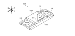
- FIG. 1 is a perspective view showing an external appearance of an electronic module 100 according to a first embodiment.
- FIG. 1 is a side view of an electronic module 100 according to a first embodiment.
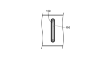
- FIG. 4 is a diagram for explaining the shape of a long hole.
- FIG. 2 is a partial exploded perspective view showing the internal structure of the electronic module 100 according to the first embodiment.
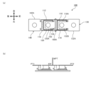
- Fig. 5A is a plan view of the electronic module 100 according to the first embodiment.
- Fig. 5B is a view showing a cross-sectional structure in the vicinity of two semiconductor elements constituting the electronic module 100 of Fig. 5A.
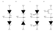
- 6A to 6C are diagrams showing examples of the connection mode when the two semiconductor elements are diodes, and Fig.
- FIG. 6D is a diagram showing an example of the connection mode when only one of the two semiconductor elements is a diode.
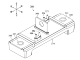
- FIG. 11 is a perspective view showing the appearance of an electronic module 300 according to a second embodiment.
- FIG. 11 is a partial exploded perspective view showing the internal structure of an electronic module 300 according to a second embodiment.
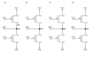
- 9A to 9D are diagrams showing examples of connection modes of two semiconductor elements when the two semiconductor elements are transistors.
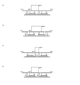
- 10A to 10C are diagrams showing an example of a cross-sectional structure in the vicinity of two semiconductor elements constituting the electronic module 300 according to the second embodiment.
- FIG. 11 is a perspective view showing the appearance of an electronic module 400 according to a third embodiment.
- FIGS. 12A to 12D are diagrams showing an example of a cross-sectional structure in the vicinity of two semiconductor elements constituting the electronic module 400 according to the third embodiment.
- FIG. 13 is a diagram showing an example of a connection mode in the case where the electronic module 100 includes four semiconductor elements.
- FIG. 1 is a diagram for explaining an electronic module according to a conventional technique.
- the long side direction of the electronic module 100 is the front-rear direction
- the short side direction is the left-right direction
- the height direction of the electronic module 100 is the up-down direction. Note that in the following explanation, the terms front, back, left, right, top, and bottom are used for convenience of explanation, and do not specify the orientation in which the electronic module 100 is attached when it is used.
- the electronic module 100 has a generally rectangular parallelepiped shape that is long in the front-to-rear direction and flat in the up-down direction.
- the electronic module 100 includes an insulating substrate 112, a first conductor portion 114 and a second conductor portion 116, a first semiconductor element 118, a second semiconductor element 120, a first power terminal 130, a second power terminal 140, an internal connection frame 152, a third power terminal 160, and a sealing resin 170.
- the insulating substrate 112 is a DCB substrate (Direct Copper Bonding substrate) in which a metal plate for heat dissipation is formed on the lower surface (rear surface) of an insulating ceramic substrate, and a first conductor portion 114 and a second conductor portion 116 are formed on the upper surface.
- the insulating substrate 112 may be a printed circuit board or the like.
- the insulating substrate 112 is formed in a rectangular flat plate shape, and is preferably disposed in the center of the longitudinal direction of the electronic module 100, i.e., the front-rear direction.
- the first conductor portion 114 and the second conductor portion 116 are conductor portions formed on the insulating substrate 112. As shown in FIG. 4, the first semiconductor element 118 is disposed on the first conductor portion 114, and the second semiconductor element 120 is disposed on the second conductor portion 116. Each of the first semiconductor element 118 and the second semiconductor element 120 is a diode.
- the first semiconductor element 118 has a cathode electrode (not shown) formed on one surface (the surface (lower surface) on the insulating substrate 112 side) and an anode electrode 118A formed on the other surface (the surface (upper surface) opposite the insulating substrate 112).
- the second semiconductor element 120 has a cathode electrode (not shown) formed on one surface (the surface (lower surface) on the insulating substrate 112 side) and an anode electrode 120A formed on the other surface (the surface (upper surface) opposite the insulating substrate 112).
- the cathode electrodes of the first semiconductor element 118 and the second semiconductor element 120 are bonded to the first conductor portion 114 and the second conductor portion 116, respectively, by a conductive bonding material.
- the first power terminal 130 and the second power terminal 140 are disposed at the front in the front-rear direction of the electronic module 100, as shown in Figures 1, 2 and 4.
- the first power terminal 130 and the second power terminal 140 are formed from a conductive flat plate material (e.g., copper plate) 132A and a flat plate material (e.g., copper plate) 142A, respectively.
- the first power terminal 130 is made of a conductive flat plate material (e.g., copper plate) 132A
- the second power terminal 140 is made of a conductive flat plate material (e.g., copper plate) 142A.
- the third power terminal 160 is formed from a conductive flat plate material (e.g., a copper plate) 160A.
- the third power terminal 160 is disposed so that the plate thickness direction is in the front-to-rear direction, and has an elongated shape with the vertical direction as the longitudinal direction.
- the third power terminal 160 is disposed above the sealing resin 170, and has a portion exposed from the sealing resin 170 and a portion covered by the sealing resin 170.
- a long hole 156 is formed in the internal connection frame 152, and the left-right width dimension of the third power terminal 160 is set to be slightly smaller than the longitudinal dimension of the long hole 156.
- the long hole 156 formed in the internal connection frame 152 extends along a direction perpendicular to the line connecting the first semiconductor element 118 and the second semiconductor element 120 in the region sandwiched between the anode electrode of the first semiconductor element 118 and the cathode electrode of the second semiconductor element 120 in a plan view.
- the lower portion of the third power terminal 160 is press-fitted into the long hole 156 of the internal connection frame 152.
- the lower portion of the third power terminal 160 is in partial contact with the internal connection frame 152 within the long hole 156 and is electrically connected to the internal connection frame 152.
- the lower end surface of the third power terminal 160 is connected to predetermined electrodes of the first semiconductor element 118 and the second semiconductor element 120 by a conductive bonding material.
- the above embodiment is for a diode module, but if the semiconductor element is a MOS transistor or an IGBT (insulated gate bipolar transistor), a signal terminal (not shown) that functions as a control terminal from the gate electrode constituting the MOS transistor or IGBT is arranged to protrude above the sealing resin 170 and is connected to an external connection member (not shown).
- the semiconductor element is a MOS transistor or an IGBT (insulated gate bipolar transistor)
- a signal terminal (not shown) that functions as a control terminal from the gate electrode constituting the MOS transistor or IGBT is arranged to protrude above the sealing resin 170 and is connected to an external connection member (not shown).
- the first semiconductor element 118 and the second semiconductor element 120 are diodes.
- the elements may be other semiconductor elements such as power MOSFETs (Metal-Oxide-Semiconductor Field-Effect Transistors) and thyristors, which will be described later, or electronic elements.
- Materials such as silicon, SiC, and GaN can be used as materials for the semiconductor elements.
- Specific examples of semiconductor elements being MOS transistors and IGBTs (Insulated Gate Bipolar Transistors) will be described later.
- Fig. 6(a) to Fig. 6(c) are diagrams showing equivalent circuit variations 1 to 3 of the electronic module 100 (diode module), respectively, and Fig. 5(b) is a diagram showing the cross-sectional structure of the diode module corresponding to the equivalent circuit of Fig. 6(a).
- the first semiconductor element 118 is the upper diode in Fig. 6(a)
- the second semiconductor element 120 is the lower diode in Fig. 6(a)
- the first semiconductor element 118 and the second semiconductor element 120 are connected in series via an internal connection frame ICF (corresponding to 150 in Fig. 5(a)) and a contact point (hereinafter referred to as a "node") MP of the midpoint power terminal MPT (corresponding to 160 in Fig. 4).
- the anode electrode A (corresponding to 118A in Fig. 4) of the upper diode is connected to the second power terminal PT2 (corresponding to 130 in Fig.
- the cathode electrode K of the upper diode is connected to the anode electrode A of the lower diode (corresponding to 120A in Fig. 4), and the cathode electrode K of the lower diode is connected to the first power terminal PT1 (corresponding to 140 in Fig. 4).
- the polarity of the lower diode may be reversed so that the cathode electrode K of the upper diode is connected to the cathode electrode K of the lower diode (see FIG. 6(b)).
- a thyristor may be used instead of the diode (see FIG. 6(c)).
- one of the two diodes for example, the upper diode
- the control terminals CT1 and CT2 in FIG. 6(c) and FIG. 6(d) are input/output nodes for control signals.
- the electronic module 100 includes a first semiconductor element 118 having two electrodes, a first electrode and a second electrode, a second semiconductor element 120 having two electrodes, a third electrode and a fourth electrode, a flat first power terminal 130 connected to one of the first and second electrodes, a flat second power terminal 140 connected to one of the third and fourth electrodes, and a flat midpoint power terminal (third power terminal 160) connected to the other of the first and second electrodes and the other of the third and fourth electrodes.
- the electronic module 100 includes a flat internal connection frame 152 that connects the other of the first and second electrodes and the other of the third and fourth electrodes, and has an elongated hole 156 for press-fitting the midpoint power terminal (third power terminal 160).
- the midpoint power terminal (third power terminal 160) is press-fitted into the elongated hole 156 of the internal connection frame 152 and stands vertically.
- the configuration of the first embodiment described above allows an electronic module having two semiconductor elements to have a reduced contact area between the midpoint power terminals of the two semiconductor elements and the internal connection frame 152, and also allows the package to be made smaller, shortening the wiring length, thereby providing an electronic module with reduced inductance and wiring resistance.
- the long hole 156 extends in a direction perpendicular to the line connecting the first semiconductor element 118 and the second semiconductor element 120 in a region sandwiched between the other of the first and second electrodes of the first semiconductor element 118 and the other of the third and fourth electrodes of the second semiconductor element 120 in a plan view. Therefore, by extending in a direction perpendicular to the line connecting the two semiconductor elements, space is created in the front-to-rear region of the internal connection frame 152 that constitutes the electronic module 100, improving the freedom of packaging (package design) and wiring design.
- the first power terminal 130, the second power terminal 140, and the internal connection frame 152 are derived from the same lead frame.
- the wiring length of the connection lines related to the first power terminal 130, the second power terminal 140, and the internal connection frame 152 can be shortened, making it possible to provide an electronic module with reduced inductance and wiring resistance.
- the electronic module 300 according to the second embodiment basically has the same configuration as the electronic module 100 according to the first embodiment, but differs from the electronic module 100 according to the first embodiment in that it uses transistors instead of diodes as semiconductor elements.
- the electronic module 300 has a generally rectangular parallelepiped shape that is long in the front-rear direction and flat in the up-down direction.
- the electronic module 300 includes a semiconductor element 320, a first power terminal 330, a second power terminal 340, a third power terminal 360, a first connection frame (internal connection frame) 332B, a second connection frame 342B, and a sealing resin 370.
- the electronic module 300 includes two semiconductor elements 320A and 320B.
- power MOSFETs Metal-Oxide-Semiconductor Field-Effect Transistors
- the semiconductor elements 320A and 320B may be disposed on one surface of the insulating substrate 312.
- the semiconductor elements 320A and 320B include electrodes (not shown) formed on one surface or both surfaces of the semiconductor substrate.
- the insulating substrate 312 is a ceramic substrate, a DCB substrate (Direct Copper Bonding substrate), with a metal plate for heat dissipation formed on the underside (back surface).
- the two semiconductor elements 320 are formed, for example, on one side of the insulating substrate 312, and a metal for heat dissipation is formed on the other side.
- the insulating substrate 312 may be a printed circuit board or the like.
- the insulating substrate 312 is formed in a rectangular flat plate shape, and is preferably disposed in the center of the front-to-rear direction, which is the longitudinal direction of the electronic module 300.
- the first power terminal 330 is disposed at the front of the electronic module 300 in the front-rear direction.
- the first power terminal 330 is composed of a conductive flat plate material, for example, a plate material 332A formed into a plate shape from a copper plate.
- the first power terminal 330 has a through hole 331 that passes through the first power terminal 330 in the up-down direction. When viewed in the up-down direction, the through hole 331 has, for example, a circular shape.
- the first connection frame 332B is electrically connected to the first power terminal 330.
- the first connection frame 332B is embedded inside the sealing resin 370.
- the first connection frame 332B is integrally formed from the same plate material 332 as the first power terminal 330. In other words, the portion of the plate material 332 that is embedded in the sealing resin 370 corresponds to the first connection frame 332B.
- the first connection frame 332B has a through hole (reference number omitted) that passes through the first connection frame 332B in the vertical direction.
- the through hole has a circular shape when viewed in the vertical direction.
- the upper end of the internal connection terminal 334 is fitted into the through hole.
- the internal connection terminal 334 connects the first connection frame 332B and the electrode of the semiconductor element 320A.
- the internal connection terminal 334 is fixed to the first connection frame 332B by, for example, press fitting.
- the shape of the through hole is not limited to a circular shape, and may be a polygon such as a hexagon.
- the second power terminal 340 is disposed at the rear of the electronic module 300 in the front-to-rear direction, as shown in FIG. 8.
- the second power terminal 340 is composed of a conductive flat plate material, for example, plate material 342A formed from a copper plate.
- the second power terminal 340 has a through hole 341 that passes through the second power terminal 340 in the up-down direction.
- the through hole 341 has, for example, a circular shape when viewed in the up-down direction.
- the second connection frame 342B is electrically connected to the second power terminal 340.
- the second connection frame 342B is embedded inside the sealing resin 370.
- the second connection frame 342B is integrally formed from the same plate material 342 as the second power terminal 340. In other words, the portion of the plate material 342 that is embedded in the sealing resin 370 corresponds to the second connection frame 342B.
- the second connection frame 342B has four through holes (reference numbers omitted) that penetrate the second connection frame 342B in the vertical direction.
- the through holes have a circular shape when viewed in the vertical direction.
- the upper ends of the internal connection electrodes 344 are fitted into each of the four through holes.
- the second connection frame 342B and electrodes (not shown) of the semiconductor element 320B are connected by the four internal connection electrodes 344.
- the internal connection electrodes 344 are fixed to the second connection frame 342B by, for example, press fitting.
- the number of the above-mentioned through holes and internal connection electrodes 344 is not limited to four, and can be any number greater than or equal to one, as long as it is possible to pass the necessary power.
- the electronic module 300 includes a third power terminal 360.
- the third power terminal 360 is formed from a conductive flat plate material, for example, a copper plate.
- the third power terminal 360 is disposed so that the plate thickness direction is in the front-to-rear direction, and has an elongated shape with the vertical direction as the longitudinal direction.
- the third power terminal 360 is disposed above the sealing resin 370, and has a portion exposed from the sealing resin 370 and a portion covered by the sealing resin 370.
- the electronic module 300 includes an internal connection frame 352.
- the internal connection frame 352 is electrically connected to the third power terminal 360.
- the internal connection frame 352 may be disposed on the same plane as the first connection frame 332B and the second connection frame 342B.
- the internal connection frame 352 has through holes (reference numerals omitted) that pass through the internal connection frame 352 in the vertical direction.
- the through holes have a circular shape when viewed in the vertical direction.
- the upper ends of the internal connection terminals 354 are fitted into the through holes.
- the internal connection terminals 354 connect the internal connection frame 352 to electrodes (not shown) of the semiconductor element 320B.
- the internal connection terminals 354 are fixed to the internal connection frame 352 by, for example, press fitting.
- Figure 9(a) is a diagram showing an equivalent circuit of semiconductor elements 320A and 320B that constitute electronic module 300
- Figure 10(a) is a diagram showing the cross-sectional structure of the electronic module corresponding to the equivalent circuit of Figure 9(a).
- the semiconductor element 320B is the first MOS transistor (the upper transistor in Figure 9(a))
- the semiconductor element 320A is the second MOS transistor (the lower transistor in Figure 9(a))
- the first MOS transistor and the second MOS transistor are connected in series via the internal connection frame ICF and the contact point (hereinafter referred to as "node") MP of the midpoint power terminal MPT (corresponding to 360 in Figure 8).
- the drain electrode of the first MOS transistor is connected to the first power terminal PT1 (corresponding to 340 in Figure 8), the source electrode S of the first MOS transistor is connected to the drain electrode D of the second MOS transistor, and the source electrode S of the second MOS transistor is connected to the second power terminal PT2 (corresponding to 330 in Figure 4).
- the source electrode S of the first MOS transistor is connected to the midpoint power terminal MPT (corresponding to 360 in FIG. 4) via the internal connection frame ICF, and the gate electrode G of the first MOS transistor is connected to the control terminal CT1 (382 in FIG. 8). And the gate electrode G of the second MOS transistor is connected to the control terminal CT2 (372 in FIG. 8).
- the polarity of the lower semiconductor element 320A may be reversed so that the source electrode S of the upper semiconductor element 320B is connected to the source electrode S of the lower semiconductor element 320A, as shown in Figures 9(c) and 10(b).
- the polarity of the upper semiconductor element 320B may be reversed so that the drain electrode D of the upper semiconductor element 320B is connected to the drain electrode D of the lower semiconductor element 320A.
- the control terminals CT1 and CT2 in Figures 9(a) to 9(d) are input/output nodes for control signals.
- FIG. 13 shows an equivalent circuit when the electronic module 300 is made up of four semiconductor elements.
- the first IGBT (upper IGBT in Figure 13) and the first SBD (upper SBD in Figure 13) are connected in parallel, and the gate electrode G of the first IGBT is connected to the control terminal CT1.
- the first IGBT and the second IGBT (lower IGBT in Figure 13) are connected in series via the internal connection frame ICF and node MP of the midpoint power terminal MPT (corresponding to 360 in Figure 8).
- the second IGBT and the second SBD (lower SBD in Figure 13) are connected in parallel, and the emitter electrode E of the second IGBT is connected to the second power terminal PT2 (corresponding to 340 in Figure 8).
- the emitter electrode E of the first IGBT is connected to the midpoint power terminal MPT (corresponding to 360 in FIG. 8) via node MP, and the gate electrode G of the first IGBT is connected to a control terminal (pin terminal not shown in FIG. 8) CT1. And the gate electrode G of the second IGBT is connected to a control terminal CT2.
- the electronic module 300 according to the second embodiment differs from the electronic module 100 according to the first embodiment in that transistors are used instead of diodes as semiconductor elements.
- the contact area of the midpoint power terminals of the two semiconductor elements with the internal connection frame 352 can be reduced and the package can be made smaller to shorten the wiring length, thereby making it possible to provide an electronic module with reduced inductance and wiring resistance.
- the long hole extends in a direction perpendicular to the line connecting the first semiconductor element 320A and the second semiconductor element 320B in a region sandwiched between the other electrode of the first semiconductor element 320A and the other electrode of the second semiconductor element 320B in a plan view. Therefore, by extending in a direction perpendicular to the line connecting the two semiconductor elements, space is created in the front-to-rear region of the internal connection frame 352 that constitutes the electronic module 300, improving the freedom of packaging (package design) and wiring design.
- the first power terminal 330, the second power terminal 340, and the internal connection frame 352 are derived from the same lead frame. Therefore, the wiring length of the connection lines connected to the first power terminal 330, the second power terminal 340, and the internal connection frame 352 can be shortened, making it possible to provide an electronic module with reduced inductance and wiring resistance.
- the first semiconductor element 320A further has a first control electrode (gate electrode)
- the second semiconductor element 320B further has a second control electrode (gate electrode)
- the electronic module 300 further includes a control terminal CT2 connected to the first control electrode of the first semiconductor element 320A and a control terminal CT1 connected to the second control electrode of the second semiconductor element 320B. Therefore, the wiring length of the connection lines connected to the first power terminal 330, the second power terminal 340, and the internal connection frame 352 can be shortened, so that an electronic module having a half-bridge structure with reduced inductance and wiring resistance can be provided.
- the long hole 256 extends in a direction parallel to the line connecting the first semiconductor element 118 and the second semiconductor element 120 in a region that does not overlap the other electrode of the first semiconductor element 118 and the other electrode of the second semiconductor element 120 in a plan view.
- the electronic module 400 according to the second embodiment is a diode module
- its cross-sectional structure is as shown in FIG. 12(d).
- the cross-sectional structure is as shown in, for example, FIG. 12(a) and FIG. 12(b).
- the cross-sectional structure is as shown in FIG. 12(c).
- the long hole 256 extends along a direction parallel to the line connecting the first semiconductor element 118 and the second semiconductor element 120 in a region that does not overlap the other of the first and second electrodes of the first semiconductor element 118 and the other of the third and fourth electrodes of the second semiconductor element 120, thereby creating space in the left-right regions of the electronic module (particularly the internal connection frame), thereby improving the freedom of packaging (package design) and wiring design.
Landscapes
- Inverter Devices (AREA)
- Lead Frames For Integrated Circuits (AREA)
Abstract
本発明の電子モジュール100は、第1電極および第2電極の2つの電極を有する第1の半導体素子118と、第3電極および第4電極の2つの電極を有する第2の半導体素子120と、第1電極および第2電極のうち他方の電極と第3電極および第4電極のうち他方の電極に接続された平板状の中点パワー端子160とを備え、第1電極および第2電極のうち他方の電極と第3電極および第4電極のうち他方の電極とを接続する平板状の内部接続フレーム152であって、中点パワー端子160を圧入するための長穴156を有する内部接続フレーム152を備える。中点パワー端子160は、内部接続フレーム152の長穴156に圧入され垂直方向に立設している。 本発明の電子モジュール100によれば、中点パワー端子のフレームに対する接触面積を小さくするとともにパッケージを小さくして配線長を短くしてインダクタンスや配線抵抗が低減される。
Description
本出願は、日本国において、2023年4月28日に出願された特願2023-074805号に基づく優先権を主張するものであり、当該出願に記載された内容はすべて参照によりそのまま本明細書に援用される。
本発明は、電子モジュールに関する。
従来、ハーフブリッジ構造を有する電子モジュール500が知られている(例えば、特許文献1参照)。上記した電子モジュールには、例えば、以下に示すような構成を有するものがある。例えば、図14に記載の電子モジュール500は、ハイサイドの第1トランジスタ(半導体素子)730と、ローサイドの第2トランジスタ(半導体素子)740と、第1トランジスタ730の第1ドレイン電極(図示せず)に接続された第1パワー端子630と、第2トランジスタ740の第2ソース電極(図示せず)に接続された第2パワー端子640と、第1トランジスタ730の第1ソース電極(図示せず)と第2トランジスタ740の第2ドレイン電極(図示せず)に接続された中点パワー端子660とを備え、ハーフブリッジ構造を有する。
しかしながら、インダクタンスや配線抵抗を低減するために、第1パワー端子630、第2パワー端子640及び中点パワー端子660を平面状の端子とするとともにこれら3つの端子にセルナット構造を適用して外部に電流を取り出すようにした場合、外部接続部材と中点パワー端子660との接続領域を確保する必要があるため、第1トランジスタ730と第2トランジスタ740の間に位置する中点パワー端子660の平面積を小さくすることは難しく、第1トランジスタ730と第2トランジスタ740との間隔を狭くすることが難しくなる。その結果、パッケージが大きくなるとともに配線長が長くなり、これに起因してインダクタンスや配線抵抗が増大してしまうという課題が生じる。なお、上記課題は、半導体チップとして、トランジスタの代わりに、トランジスタ以外の3電極半導体チップ(例えばサイリスタ)や2電極半導体チップ(例えばダイオード)を用いた場合にも上記同様の課題が生じる。
そこで、本発明は上記課題に鑑みてなされたものであり、2つの半導体チップを備える電子モジュールにおいて、外部接続部材と中点パワー端子との接続領域を確保しながら、インダクタンスや配線抵抗を低減することが可能な電子モジュールを提供することを目的とする。
本発明の電子モジュールは、第1電極および第2電極の2つの電極を有する第1の半導体素子と、第3電極および第4電極の2つの電極を有する第2の半導体素子と、前記第1電極および前記第2電極のうち一方の電極に接続された平板状の第1パワー端子と、前記第3電極および前記第4電極のうち一方の電極に接続された平板状の第2パワー端子と、前記第1電極および前記第2電極のうち他方の電極と前記第3電極および前記第4電極のうち他方の電極に接続された平板状の中点パワー端子とを備える電子モジュールであって、前記電子モジュールは、前記第1電極および前記第2電極のうち前記他方の電極と前記第3電極および前記第4電極のうち前記他方の電極とを接続する平板状の内部接続フレームであって、前記中点パワー端子を圧入するための長穴を有する内部接続フレームをさらに備え、前記中点パワー端子は、前記内部接続フレームの前記長穴に圧入され垂直方向に立設していることを特徴とする。
本発明の電子モジュールによれば、中点パワー端子が、上記した内部接続フレームの長穴に圧入され垂直方向に立設しているものであることから、外部接続部材と中点パワー端子660との接続領域を確保することができる。
また、第1の半導体素子と第2の半導体素子との設置間隔を狭くできる。このため、パッケージを小さくするとともに配線長も短くできるため、インダクタンスや配線抵抗が低減することができる。
(第1の実施形態)
以下、本発明の第1の実施形態に係る電子モジュールについて、電子モジュールとしてダイオードモジュールを例に挙げて説明する。以下に説明する実施形態は、特許請求の範囲に係る発明を限定するものではない。また、実施形態の中で説明されている諸要素及びその組み合わせの全てが本発明に必須であるとは限らない。
以下、本発明の第1の実施形態に係る電子モジュールについて、電子モジュールとしてダイオードモジュールを例に挙げて説明する。以下に説明する実施形態は、特許請求の範囲に係る発明を限定するものではない。また、実施形態の中で説明されている諸要素及びその組み合わせの全てが本発明に必須であるとは限らない。
以下の説明において、図1~図2に示すように、電子モジュール100の長手方向を前後方向とし、短手方向を左右方向として説明する。また、電子モジュール100の高さ方向を上下方向として説明する。なお、以下の説明における、前、後、左、右、上、下は、説明のために便宜上使用するものであり、電子モジュール100を使用するときに、電子モジュール100が取り付けられる向きを特定するものではない。
電子モジュール100は、図1~図4に示すように、前後方向に長尺で、かつ上下方向に扁平な略直方体形状をなしている。電子モジュール100は、絶縁基板112と、第1導体部114及び第2導体部116と、第1の半導体素子118と、第2の半導体素子120と、第1パワー端子130と、第2パワー端子140と、内部接続フレーム152と、第3パワー端子160と、封止樹脂170とを備えている。
絶縁基板112は、セラミック製の絶縁性基板の下面(裏面)に放熱用の金属板が形成され、上面に第1導体部114及び第2導体部116が形成されたDCB基板(Direct Copper Bonding基板)である。なお、絶縁基板112は、プリント基板等であってもよい。絶縁基板112は、矩形の平板状に形成されており、電子モジュール100の長手方向である前後方向の中央部に配設されていることが好ましい。
第1導体部114及び第2導体部116は、絶縁基板112上に形成された導体部である。図4に示されるように、第1導体部114上には第1の半導体素子118が配置されており、第2導体部116上には第2の半導体素子120が配置されている。第1の半導体素子118および第2の半導体素子120のそれぞれはダイオードである。第1の半導体素子118は一方の面(絶縁基板112側の面(下面))に形成された図示しないカソード電極と、他方の面(絶縁基板112とは反対側の面(上面))に形成されたアノード電極118Aを有している。第2の半導体素子120は一方の面(絶縁基板112側の面(下面))に形成された図示しないカソード電極と、他方の面(絶縁基板112とは反対側の面(上面))に形成されたアノード電極120Aを有している。第1の半導体素子118および第2の半導体素子120のカソード電極は、それぞれ第1導体部114および第2導体部116に対して導電性接合材によって接合されている。
第1パワー端子130および第2パワー端子140は、図1,図2および図4に示すように、電子モジュール100の前後方向の前方に配設されている。第1パワー端子130および第2パワー端子140は、それぞれ導電性を有する平板材(例えば銅板)132Aおよび平板材(例えば銅板)142Aにより形成される。第1パワー端子130は、導電性を有する平板材(例えば銅板)132Aから構成され、第2パワー端子140は、導電性を有する平板材(例えば銅板)142Aから構成される。
第3パワー端子160は、図1,図2および図4に示されるように、導電性を有する平板材(例えば銅板)160Aにより形成される。第3パワー端子160は、前後方向が板厚方向となるように配設されており、上下方向を長手方向とする長尺状をなしている。第3パワー端子160は、封止樹脂170の上側に配設され、封止樹脂170から露出する部分と、封止樹脂170に覆われた部分とを有する。
内部接続フレーム152には図3に示すように長穴156が形成されており、第3パワー端子160の左右方向の幅寸法は長穴156の長手方向寸法より若干小さく設定されている。内部接続フレーム152に形成される長穴156は、平面的に見て第1の半導体素子118のアノード電極と第2の半導体素子120のカソード電極に挟まれた領域において、第1の半導体素子118と第2の半導体素子120とを結ぶ線に直交する方向に沿って延在する。
第3パワー端子160の下側部分は、内部接続フレーム152の長穴156に圧入されている。第3パワー端子160の下側部分は、長穴156内において内部接続フレーム152と部分的に接触しており、内部接続フレーム152と電気的に接続されている。第3パワー端子160の下端面は、導電性接合材によって第1の半導体素子118および第2の半導体素子120の所定の電極と接続されている。
なお、上記した実施形態はダイオードモジュールの場合であるが、半導体素子がMOSトランジスタやIGBT(絶縁ゲート型バイポーラトランジスタ)であるような場合には、MOSトランジスタやIGBTを構成するゲート電極から制御端子として機能する信号端子(図示せず)が、封止樹脂170の上方に突出するよう配設され、図示しない外部接続部材と接続される。
第1の半導体素子118と第2の半導体素子120は、本第1の実施形態では、ダイオードである。素子はダイオード以外にも例えば、後述するパワーMOSFET(Metal-Oxide-Semiconductor Field-Effect Transistor)、サイリスタ等の他の半導体素子や、電子素子であってもよい。また、半導体素子の材料としては、シリコン、SiC、GaN等の素材を用いることができる。なお、半導体素子がMOSトランジスタやIGBT(絶縁ゲート型バイポーラトランジスタ)である場合の具体例は後述する。
(ダイオードモジュールにおける半導体素子の等価回路および断面構造)
以下に、電子モジュールをダイオードモジュールとした場合における半導体素子の等価回路および断面構造について図5(b)、図6(a)~図6(c)を参照して説明する。図6(a)~図6(c)はそれぞれ電子モジュール100(ダイオードモジュール)の等価回路バリエーション1~3を示した図であり、図5(b)は図6(a)の等価回路に対応するダイオードモジュールの断面構造を示した図である。
以下に、電子モジュールをダイオードモジュールとした場合における半導体素子の等価回路および断面構造について図5(b)、図6(a)~図6(c)を参照して説明する。図6(a)~図6(c)はそれぞれ電子モジュール100(ダイオードモジュール)の等価回路バリエーション1~3を示した図であり、図5(b)は図6(a)の等価回路に対応するダイオードモジュールの断面構造を示した図である。
[接続バリエーション]
図5および図6(a)に示すように、第1の半導体素子118を図6(a)の上側ダイオードとし、第2の半導体素子120を図6(a)の下側ダイオードとして、第1の半導体素子118および第2の半導体素子120が内部接続フレームICF(図5(a)の150に相当)および中点パワー端子MPT(図4の160に相当)の接点(以下「ノード」と呼ぶ。)MPを介して直列接続されている。そして上側ダイオードのアノード電極A(図4の118Aに相当)が第2のパワー端子PT2(図4の130に相当)に接続され、上側ダイオードのカソード電極Kが下側ダイオードのアノード電極A(図4の120Aに相当)に接続され、下側ダイオードのカソード電極Kが第1のパワー端子PT1(図4の140に相当)に接続されている。
図5および図6(a)に示すように、第1の半導体素子118を図6(a)の上側ダイオードとし、第2の半導体素子120を図6(a)の下側ダイオードとして、第1の半導体素子118および第2の半導体素子120が内部接続フレームICF(図5(a)の150に相当)および中点パワー端子MPT(図4の160に相当)の接点(以下「ノード」と呼ぶ。)MPを介して直列接続されている。そして上側ダイオードのアノード電極A(図4の118Aに相当)が第2のパワー端子PT2(図4の130に相当)に接続され、上側ダイオードのカソード電極Kが下側ダイオードのアノード電極A(図4の120Aに相当)に接続され、下側ダイオードのカソード電極Kが第1のパワー端子PT1(図4の140に相当)に接続されている。
なお、変形例として下側ダイオードの極性を逆にして上側ダイオードのカソード電極Kが下側ダイオードのカソード電極Kに接続するようにしてもよい(図6(b)参照)。また、他の変形例としてダイオードの代わりにサイリスタを用いてもよい(図6(c)参照)。さらに他の変形例として、純粋なダイオードモジュールではないが2つのダイオードの一方(例えば、上側ダイオード)をMOSトランジスタに代えてもよい(図6(d)参照)。なお、図6(c)および図6(d)の制御端子CT1,CT2は制御信号の入出力ノードである。
[第1の実施形態における効果]
第1の実施形態に係る電子モジュール100は、第1電極および第2電極の2つの電極を有する第1の半導体素子118と、第3電極および第4電極の2つの電極を有する第2の半導体素子120と、第1電極および第2電極のうち一方の電極に接続された平板状の第1パワー端子130と、第3電極および第4電極のうち一方の電極に接続された平板状の第2パワー端子140と、第1電極および第2電極のうち他方の電極と第3電極および第4電極のうち他方の電極に接続された平板状の中点パワー端子(第3パワー端子160)とを備える。電子モジュール100は、第1電極および第2電極のうち他方の電極と第3電極および第4電極のうち他方の電極とを接続する平板状の内部接続フレーム152であって、中点パワー端子(第3パワー端子160)を圧入するための長穴156を有する内部接続フレーム152を備える。中点パワー端子(第3パワー端子160)は、内部接続フレーム152の長穴156に圧入され垂直方向に立設している。
第1の実施形態に係る電子モジュール100は、第1電極および第2電極の2つの電極を有する第1の半導体素子118と、第3電極および第4電極の2つの電極を有する第2の半導体素子120と、第1電極および第2電極のうち一方の電極に接続された平板状の第1パワー端子130と、第3電極および第4電極のうち一方の電極に接続された平板状の第2パワー端子140と、第1電極および第2電極のうち他方の電極と第3電極および第4電極のうち他方の電極に接続された平板状の中点パワー端子(第3パワー端子160)とを備える。電子モジュール100は、第1電極および第2電極のうち他方の電極と第3電極および第4電極のうち他方の電極とを接続する平板状の内部接続フレーム152であって、中点パワー端子(第3パワー端子160)を圧入するための長穴156を有する内部接続フレーム152を備える。中点パワー端子(第3パワー端子160)は、内部接続フレーム152の長穴156に圧入され垂直方向に立設している。
上記した第1の実施形態の構成によれば、2個の半導体素子を備える電子モジュールにおいて、2個の半導体素子の中点パワー端子の内部接続フレーム152に対する接触面積を小さくするとともにパッケージを小さくして配線長を短くすることできるので、インダクタンスや配線抵抗が低減された電子モジュールを提供することができる。
さらに、長穴156は、平面的に見て第1の半導体素子118の第1電極および第2電極のうち他方の電極と第2の半導体素子120の第3電極および第4電極のうち他方の電極とに挟まれた領域において、第1の半導体素子118と第2の半導体素子120とを結ぶ線に直交する方向に沿って延在している。したがって、2個の半導体素子同士を結ぶ線に直交する方向に沿って延在させることによって電子モジュール100を構成する内部接続フレーム152の前後方向の領域にスペースができるためパッケージング(パッケージの設計)や配線設計の自由度が向上する。
さらに、第1パワー端子130、第2パワー端子140及び内部接続フレーム152は、同じリードフレーム由来のものであることが好ましい。すなわち複数のリードフレームにまたがって第1パワー端子130と第2パワー端子140が接続されて場合に比較して、第1パワー端子130、第2パワー端子140及び内部接続フレーム152に関係する接続線の配線長を短くすることできるので、インダクタンスや配線抵抗が低減された電子モジュールを提供することができる。
(第2の実施形態)
第2の実施形態に係る電子モジュール300は、基本的には第1の実施形態に係る電子モジュール100と同様の構成を有するが、半導体素子としてダイオードの代わりにトランジスタを用いる点で第1の実施形態に係る電子モジュール100と異なる。
第2の実施形態に係る電子モジュール300は、基本的には第1の実施形態に係る電子モジュール100と同様の構成を有するが、半導体素子としてダイオードの代わりにトランジスタを用いる点で第1の実施形態に係る電子モジュール100と異なる。
第2の実施形態に係る電子モジュール300は、図7および図8に示すように、前後方向に長尺で、かつ上下方向に扁平な略直方体形状をなしている。電子モジュール300は、半導体素子320と、第1パワー端子330と、第2パワー端子340と、第3パワー端子360と、第1接続フレーム(内部接続フレーム)332Bと、第2接続フレーム342Bと、封止樹脂370とを含んで構成される。
電子モジュール300は、2つの半導体素子320A,320Bを備える。半導体素子320A,320Bとしては、例えば、パワーMOSFET(Metal-Oxide-Semiconductor Field-Effect Transistor)を用いることができる。半導体素子320A,320Bは、絶縁基板312の一方の面上に配設されていてもよい。半導体素子320A,320Bは、半導体基板の一方の面又は両方の面に形成された図示しない電極を備える。
絶縁基板312は、下面(裏面)に放熱用の金属板が形成されたDCB基板(Direct Copper Bonding基板)のセラミックス基板である。2つの半導体素子320は、例えば、絶縁基板312の一方の面に形成され、もう一方の面に放熱用の金属が形成されている。なお、絶縁基板312は、プリント基板等であってもよい。絶縁基板312は、矩形の平板状に形成されており、電子モジュール300の長手方向である前後方向の中央部に配設されていることが好ましい。
第1パワー端子330は、図7に示すように、電子モジュール300の前後方向の前方に配設されている。第1パワー端子330は、導電性を有する平板材、例えば銅板によって板状に形成された板材332Aから構成される。第1パワー端子330は、第1パワー端子330を上下方向に貫通する貫通孔331を備える。貫通孔331は、上下方向に見たとき、例えば、円形形状をなしている。
第1接続フレーム332Bは、第1パワー端子330と電気的に接続されている。第1接続フレーム332Bは、封止樹脂370の内部に埋まっている。電子モジュール300において、第1接続フレーム332Bは、第1パワー端子330と同じ板材332により、一体に形成されている。すなわち、板材332のうち、封止樹脂370に埋まっている部分が第1接続フレーム332Bに該当する。
第1接続フレーム332Bは、第1接続フレーム332Bを上下方向に貫通する貫通孔(符号省略)を備える。貫通孔は、上下方向に見たとき円形形状をなしている。貫通孔には、内部接続端子334の上端部が嵌合している。内部接続端子334により、第1接続フレーム332Bと半導体素子320Aの電極とが接続されている。内部接続端子334は、例えば圧入によって、第1接続フレーム332Bに固定されている。なお、貫通孔の形状は、円形形状に限られず、六角形等の多角形であってもよい。
第2パワー端子340は、図8に示すように、電子モジュール300の前後方向の後方に配設されている。第2パワー端子340は、導電性を有する平板材、例えば銅板から形成された板材342Aから構成される。第2パワー端子340は、第2パワー端子340を上下方向に貫通する貫通孔341を備える。貫通孔341は、上下方向に見たとき、例えば、円形形状をなしている。
第2接続フレーム342Bは、第2パワー端子340と電気的に接続されている。第2接続フレーム342Bは、封止樹脂370の内部に埋まっている。電子モジュール300において、第2接続フレーム342Bは、第2パワー端子340と同じ板材342により、一体に形成されている。すなわち、板材342のうち、封止樹脂370に埋まっている部分が、第2接続フレーム342Bに該当する。
第2接続フレーム342Bは、第2接続フレーム342Bを上下方向に貫通する4つの貫通孔(符号省略)を備える。貫通孔は、上下方向に見たとき円形形状をなしている。4つの貫通孔には、それぞれ、内部接続電極344の上端部が嵌合している。4つの内部接続電極344により、第2接続フレーム342Bと半導体素子320Bの図示しない電極とが接続されている。内部接続電極344は、例えば圧入によって、第2接続フレーム342Bに固定されている。上記した貫通孔及び内部接続電極344の数は、必要な電力を流通することが可能であれば4個に限られず、1個以上の任意の数であることができる。
電子モジュール300は第3パワー端子360を備えている。第3パワー端子360は、図8に示されるように、導電性を有する平板材、例えば、銅板により形成されている。第3パワー端子360は、前後方向が板厚方向となるように配設されており、上下方向を長手方向とする長尺状をなしている。第3パワー端子360は、封止樹脂370の上側に配設され、封止樹脂370から露出する部分と、封止樹脂370に覆われた部分とを有する。
電子モジュール300は、内部接続フレーム352を備えている。内部接続フレーム352は、第3パワー端子360と電気的に接続されている。内部接続フレーム352は、第1接続フレーム332B及び第2接続フレーム342Bと同じ平面上に配設されていてもよい。
内部接続フレーム352は、内部接続フレーム352を上下方向に貫通する貫通孔(符号省略)を備える。貫通孔は、上下方向に見たとき円形形状をなしている。貫通孔には、内部接続端子354の上端部が嵌合している。内部接続端子354により、内部接続フレーム352と半導体素子320Bの図示しない電極とが接続されている。内部接続端子354は、例えば圧入によって、内部接続フレーム352に固定されている。
(接続バリエーション)
以下に、半導体素子がMOSトランジスタである場合における等価回路および断面構造について図9(a)~(d)および図10(a)~(c)を参照して説明する。図9(a)は電子モジュール300を構成する半導体素子320A、320Bの等価回路を示した図であり、図10(a)は図9(a)の等価回路に対応する電子モジュールの断面構造を示した図である。
以下に、半導体素子がMOSトランジスタである場合における等価回路および断面構造について図9(a)~(d)および図10(a)~(c)を参照して説明する。図9(a)は電子モジュール300を構成する半導体素子320A、320Bの等価回路を示した図であり、図10(a)は図9(a)の等価回路に対応する電子モジュールの断面構造を示した図である。
図9(a)および図10(a)に示すように、半導体素子320Bを第1のMOSトランジスタ(図9(a)の上側トランジスタ)とし、半導体素子320Aを第2のMOSトランジスタ(図9(a)の下側トランジスタ)として、第1のMOSトランジスタおよび第2のMOSトランジスタが内部接続フレームICFおよび中点パワー端子MPT(図8では360に相当)の接点(以下「ノード」と呼ぶ。)MPを介して直列接続されている。そして第1のMOSトランジスタのドレイン電極が第1のパワー端子PT1(図8の340に相当)に接続され、第1のMOSトランジスタのソース電極Sが第2のMOSトランジスタのドレイン電極Dに接続され、第2のMOSトランジスタのソース電極Sが第2のパワー端子PT2(図4の330に相当)に接続されている。
また、第1のMOSトランジスタのソース電極Sが内部接続フレームICFを介して中点パワー端子MPT(図4では360に相当)に接続され、第1のMOSトランジスタのゲート電極Gが制御端子(図8の382)CT1に接続されている。そして第2のMOSトランジスタのゲート電極Gが制御端子(図8の372)CT2に接続されている。
なお、変形例として上記した構成が上側の半導体素子320B(上側トランジスタ)と下側の半導体素子320A(下側トランジスタ)が順方向(上側トランジスタのソース電極Sが下側トランジスタのドレイン電極Dに接続)に接続されたものであるのに対し、図9(c)および図10(b)に示すように下側の半導体素子320Aの極性を逆にして上側の半導体素子320Bのソース電極Sが下側の半導体素子320Aのソース電極Sに接続するようにしてもよい。また、他の変形例として図9(d)に示すように、上側の半導体素子320Bの極性を逆にして上側の半導体素子320Bのドレイン電極Dが下側の半導体素子320Aのドレイン電極Dに接続するようにしてもよい。なお、図9(a)~図9(d)の制御端子CT1やCT2は制御信号の入出力ノードである。
次に図9(c)および図10(b)の構成においてMOSトランジスタをIGBTに置き換えた場合における等価回路および断面構造について図9(b)、図10(c)に示されているが、上記トランジスタをIGBTに変えた以外は同じであるので説明を省略する。なお、図示した態様以外の他の接続態様(等価回路及び断面)についても上記同様である。
次に、半導体素子がIGBTとショットキーバリアダイオード(以下、「SBD」と呼ぶ。)である場合における等価回路について図13を参照して説明する。図13は電子モジュール300を構成する半導体素子が4個の場合の等価回路を示した図である。
図13に示すように、第1のIGBT(図13の上側IGBT)と第1のSBD(図13の上側SBD)が並列接続され、第1のIGBTのゲート電極Gが制御端子CT1に接続されている。第1のIGBTおよび第2のIGBT(図13の下側IGBT)は内部接続フレームICFおよび中点パワー端子MPT(図8では360に相当)のノードMPを介して直列接続されている。そして第2のIGBTと第2のSBD(図13の下側SBD)が並列接続され、第2のIGBTのエミッタ電極Eが第2のパワー端子PT2(図8の340に相当)に接続されている。また、第1のIGBTのエミッタ電極EがノードMPを介して中点パワー端子MPT(図8では360に相当)に接続され、第1のIGBTのゲート電極Gが制御端子(図8に図示しないピン端子)CT1に接続されている。そして第2のIGBTのゲート電極Gが制御端子CT2に接続されている。
[第2の実施形態における効果]
このように、第2の実施形態に係る電子モジュール300は、半導体素子としてダイオードの代わりにトランジスタを用いる点で第1の実施形態に係る電子モジュール100とは異なるが、第1の実施形態に係る電子モジュール100と同様に、2個の半導体素子を備える電子モジュールにおいて、2個の半導体素子の中点パワー端子の内部接続フレーム352に対する接触面積を小さくするとともにパッケージを小さくして配線長を短くすることできるので、インダクタンスや配線抵抗が低減された電子モジュールを提供することができる。
このように、第2の実施形態に係る電子モジュール300は、半導体素子としてダイオードの代わりにトランジスタを用いる点で第1の実施形態に係る電子モジュール100とは異なるが、第1の実施形態に係る電子モジュール100と同様に、2個の半導体素子を備える電子モジュールにおいて、2個の半導体素子の中点パワー端子の内部接続フレーム352に対する接触面積を小さくするとともにパッケージを小さくして配線長を短くすることできるので、インダクタンスや配線抵抗が低減された電子モジュールを提供することができる。
さらに、長穴は、平面的に見て第1の半導体素子320Aの他方の電極と第2の半導体素子320Bの他方の電極に挟まれた領域において、第1の半導体素子320Aと第2の半導体素子320Bとを結ぶ線に直交する方向に沿って延在している。したがって、2個の半導体素子同士を結ぶ線に直行する方向に沿って延在させることによって電子モジュール300を構成する内部接続フレーム352の前後方向の領域にスペースができるためパッケージング(パッケージの設計)や配線設計の自由度が向上する。
さらに、第1パワー端子330、第2パワー端子340及び内部接続フレーム352は、同じリードフレーム由来のものであることが好ましい。したがって、第1パワー端子330、第2パワー端子340及び内部接続フレーム352に接続される接続線の配線長を短くすることできるので、インダクタンスや配線抵抗が低減された電子モジュールを提供することができる。
さらに、第1の半導体素子320Aは、第1制御電極(ゲート電極)をさらに有し、第2の半導体素子320Bは、第2制御電極(ゲート電極)をさらに有し、電子モジュール300は、第1の半導体素子320Aの第1制御電極に接続された制御端子CT2と、第2の半導体素子320Bの第2制御電極に接続された制御端子CT1とをさらに備える。したがって、第1パワー端子330、第2パワー端子340及び内部接続フレーム352に接続される接続線の配線長を短くすることできるので、インダクタンスや配線抵抗が低減されたハーフブリッジ構造を有する電子モジュールを提供することができる。
(第3の実施形態)
以下、本発明の第3の実施形態に係る電子モジュールについて、図11、図12(a)~(d)を参照して説明する。なお、この第3の実施形態は、上記した第1の実施形態と以下の点を除いて同様であるので異なる点についてのみ説明し同様の部分の説明は省略する。また、異なる点以外の符号は区別する必要がないため第1の実施形態で用いた符号と同様の符号を用いる。
以下、本発明の第3の実施形態に係る電子モジュールについて、図11、図12(a)~(d)を参照して説明する。なお、この第3の実施形態は、上記した第1の実施形態と以下の点を除いて同様であるので異なる点についてのみ説明し同様の部分の説明は省略する。また、異なる点以外の符号は区別する必要がないため第1の実施形態で用いた符号と同様の符号を用いる。
長穴256は、平面的に見て第1の半導体素子118の他方の電極と第2の半導体素子120の前記他方の電極に重ならない領域において、第1の半導体素子118と第2の半導体素子120とを結ぶ線に平行な方向に沿って延在している。ここで、第2の実施形態に係る電子モジュール400がダイオードモジュールである場合にはその断面構造は図12(d)に示すとおりである。電子モジュール400における2個の半導体素子が共にMOSトランジスタである場合の断面構造は例えば、図12(a)、図12(b)に示すとおりである。電子モジュール400における2個の半導体素子が共にIGBTである場合の断面構造は図12(c)に示すとおりである。
[第3の実施形態における効果]
長穴256は、第1の半導体素子118の第1電極および第2電極のうち他方の電極と第2の半導体素子120の第3電極および第4電極のうち他方の電極に重ならない領域において、第1の半導体素子118と第2の半導体素子120とを結ぶ線に平行な方向に沿って延在しているので、電子モジュール(特に内部接続フレーム)の左右方向の領域にスペースができるためパッケージング(パッケージの設計)や配線設計の自由度が向上する。
長穴256は、第1の半導体素子118の第1電極および第2電極のうち他方の電極と第2の半導体素子120の第3電極および第4電極のうち他方の電極に重ならない領域において、第1の半導体素子118と第2の半導体素子120とを結ぶ線に平行な方向に沿って延在しているので、電子モジュール(特に内部接続フレーム)の左右方向の領域にスペースができるためパッケージング(パッケージの設計)や配線設計の自由度が向上する。
100,300,400…電子モジュール、112,312…絶縁基板、118,120,320A,320B、…半導体素子、130,330…第1パワー端子、132A,142A,160A,332A,342,360…平板材、140,340…第2パワー端子、152,352…内部接続フレーム、156,256,356…長穴、160,360…第3パワー端子、170,370…封止樹脂
Claims (5)
- 第1電極および第2電極の2つの電極を有する第1の半導体素子と、
第3電極および第4電極の2つの電極を有する第2の半導体素子と、
前記第1電極および前記第2電極のうち一方の電極に接続された平板状の第1パワー端子と、
前記第3電極および前記第4電極のうち一方の電極に接続された平板状の第2パワー端子と、
前記第1電極および前記第2電極のうち他方の電極と前記第3電極および前記第4電極のうち他方の電極に接続された平板状の中点パワー端子とを備える電子モジュールであって、
前記電子モジュールは、前記第1電極および前記第2電極のうち前記他方の電極と前記第3電極および前記第4電極のうち前記他方の電極とを接続する平板状の内部接続フレームであって、前記中点パワー端子を圧入するための長穴を有する内部接続フレームをさらに備え、
前記中点パワー端子は、前記内部接続フレームの前記長穴に圧入され垂直方向に立設していることを特徴とする電子モジュール。 - 前記長穴は、平面的に見て前記第1電極および前記第2電極のうち前記他方の電極と前記第3電極および前記第4電極のうち前記他方の電極とに挟まれた領域において、前記第1の半導体素子と前記第2の半導体素子とを結ぶ線に直交する方向に沿って延在することを特徴とする請求項1に記載の電子モジュール。
- 前記長穴は、平面的に見て前記第1電極および前記第2電極のうち前記他方の電極と前記第3電極および前記第4電極のうち前記他方の電極に重ならない領域において、前記第1の半導体素子と前記第2の半導体素子とを結ぶ線に平行な方向に沿って延在することを特徴とする請求項1に記載の電子モジュール。
- 前記第1パワー端子、前記第2パワー端子及び前記内部接続フレームは、同じリードフレーム由来のものであることを特徴とする請求項1に記載の電子モジュール。
- 前記第1の半導体素子は、第1制御電極をさらに有し、
前記第2の半導体素子は、第2制御電極をさらに有し、
前記電子モジュールは、
前記第1の半導体素子の前記第1制御電極に接続された第1制御端子と、
前記第2の半導体素子の前記第2制御電極に接続された第2制御端子とをさらに備え、ハーフブリッジ構造を有することを特徴とする請求項1に記載の電子モジュール。
Priority Applications (2)
| Application Number | Priority Date | Filing Date | Title |
|---|---|---|---|
| DE112024001854.8T DE112024001854T5 (de) | 2023-04-28 | 2024-04-17 | Elektronikmodul |
| CN202480028656.6A CN121014111A (zh) | 2023-04-28 | 2024-04-17 | 电子模块 |
Applications Claiming Priority (2)
| Application Number | Priority Date | Filing Date | Title |
|---|---|---|---|
| JP2023074805A JP2024159062A (ja) | 2023-04-28 | 2023-04-28 | 電子モジュール |
| JP2023-074805 | 2023-04-28 |
Publications (1)
| Publication Number | Publication Date |
|---|---|
| WO2024225129A1 true WO2024225129A1 (ja) | 2024-10-31 |
Family
ID=93256309
Family Applications (1)
| Application Number | Title | Priority Date | Filing Date |
|---|---|---|---|
| PCT/JP2024/015219 Ceased WO2024225129A1 (ja) | 2023-04-28 | 2024-04-17 | 電子モジュール |
Country Status (4)
| Country | Link |
|---|---|
| JP (1) | JP2024159062A (ja) |
| CN (1) | CN121014111A (ja) |
| DE (1) | DE112024001854T5 (ja) |
| WO (1) | WO2024225129A1 (ja) |
Citations (4)
| Publication number | Priority date | Publication date | Assignee | Title |
|---|---|---|---|---|
| WO2014174854A1 (ja) * | 2013-04-25 | 2014-10-30 | 富士電機株式会社 | 半導体装置 |
| JP2017050374A (ja) * | 2015-09-01 | 2017-03-09 | ローム株式会社 | パワーモジュール、パワーモジュールの放熱構造、およびパワーモジュールの接合方法 |
| JP2017204580A (ja) * | 2016-05-12 | 2017-11-16 | ローム株式会社 | パワーモジュール、パワーモジュールの連結構造体、および電気自動車またはハイブリッドカー |
| JP2021068859A (ja) * | 2019-10-28 | 2021-04-30 | 富士電機株式会社 | 半導体モジュール |
-
2023
- 2023-04-28 JP JP2023074805A patent/JP2024159062A/ja active Pending
-
2024
- 2024-04-17 CN CN202480028656.6A patent/CN121014111A/zh active Pending
- 2024-04-17 DE DE112024001854.8T patent/DE112024001854T5/de active Pending
- 2024-04-17 WO PCT/JP2024/015219 patent/WO2024225129A1/ja not_active Ceased
Patent Citations (4)
| Publication number | Priority date | Publication date | Assignee | Title |
|---|---|---|---|---|
| WO2014174854A1 (ja) * | 2013-04-25 | 2014-10-30 | 富士電機株式会社 | 半導体装置 |
| JP2017050374A (ja) * | 2015-09-01 | 2017-03-09 | ローム株式会社 | パワーモジュール、パワーモジュールの放熱構造、およびパワーモジュールの接合方法 |
| JP2017204580A (ja) * | 2016-05-12 | 2017-11-16 | ローム株式会社 | パワーモジュール、パワーモジュールの連結構造体、および電気自動車またはハイブリッドカー |
| JP2021068859A (ja) * | 2019-10-28 | 2021-04-30 | 富士電機株式会社 | 半導体モジュール |
Also Published As
| Publication number | Publication date |
|---|---|
| DE112024001854T5 (de) | 2026-02-12 |
| CN121014111A (zh) | 2025-11-25 |
| JP2024159062A (ja) | 2024-11-08 |
Similar Documents
| Publication | Publication Date | Title |
|---|---|---|
| JP6650061B2 (ja) | スイッチングデバイス | |
| JP7731523B1 (ja) | 半導体モジュール | |
| JP7481343B2 (ja) | 半導体装置 | |
| KR102350735B1 (ko) | 2개의 직렬-연결된 칩들의 스택으로 형성된 집적 회로 | |
| JP7799880B2 (ja) | 半導体装置、および半導体装置の製造方法 | |
| CN110600457B (zh) | 半导体装置 | |
| US20240404977A1 (en) | Semiconductor device and semiconductor module | |
| JP2026015612A (ja) | 半導体装置 | |
| US20240186256A1 (en) | Semiconductor device | |
| WO2022259824A1 (ja) | 接合構造および半導体装置 | |
| US20240047433A1 (en) | Semiconductor device | |
| WO2024225129A1 (ja) | 電子モジュール | |
| JP4695041B2 (ja) | 半導体装置 | |
| JP2024051117A (ja) | 半導体ユニット及び半導体装置 | |
| WO2024029336A1 (ja) | 半導体装置 | |
| WO2023243464A1 (ja) | 半導体装置、半導体モジュール、および半導体モジュールの取付構造 | |
| WO2023017708A1 (ja) | 半導体装置 | |
| US20250167163A1 (en) | Semiconductor device | |
| US20230260869A1 (en) | Semiconductor device | |
| US20240203849A1 (en) | Semiconductor device and mounting structure for semiconductor device | |
| US20260026406A1 (en) | Semiconductor arrangement | |
| US20240136320A1 (en) | Semiconductor device | |
| JP2025185284A (ja) | 半導体装置および半導体モジュール | |
| WO2025258458A1 (ja) | 半導体装置および半導体モジュール | |
| WO2025258436A1 (ja) | 半導体モジュールの製造方法、および半導体モジュール |
Legal Events
| Date | Code | Title | Description |
|---|---|---|---|
| 121 | Ep: the epo has been informed by wipo that ep was designated in this application |
Ref document number: 24796882 Country of ref document: EP Kind code of ref document: A1 |
|
| WWE | Wipo information: entry into national phase |
Ref document number: 112024001854 Country of ref document: DE |
|
| WWP | Wipo information: published in national office |
Ref document number: 112024001854 Country of ref document: DE |