WO2024224941A1 - 配線回路基板、電気的要素実装基板、電子機器および配線回路基板の製造方法 - Google Patents
配線回路基板、電気的要素実装基板、電子機器および配線回路基板の製造方法 Download PDFInfo
- Publication number
- WO2024224941A1 WO2024224941A1 PCT/JP2024/013309 JP2024013309W WO2024224941A1 WO 2024224941 A1 WO2024224941 A1 WO 2024224941A1 JP 2024013309 W JP2024013309 W JP 2024013309W WO 2024224941 A1 WO2024224941 A1 WO 2024224941A1
- Authority
- WO
- WIPO (PCT)
- Prior art keywords
- layer
- hole
- support
- support layer
- terminal
- Prior art date
- Legal status (The legal status is an assumption and is not a legal conclusion. Google has not performed a legal analysis and makes no representation as to the accuracy of the status listed.)
- Ceased
Links
Images








Classifications
-
- H—ELECTRICITY
- H05—ELECTRIC TECHNIQUES NOT OTHERWISE PROVIDED FOR
- H05K—PRINTED CIRCUITS; CASINGS OR CONSTRUCTIONAL DETAILS OF ELECTRIC APPARATUS; MANUFACTURE OF ASSEMBLAGES OF ELECTRICAL COMPONENTS
- H05K1/00—Printed circuits
- H05K1/02—Details
- H05K1/11—Printed elements for providing electric connections to or between printed circuits
- H05K1/115—Via connections; Lands around holes or via connections
-
- H—ELECTRICITY
- H05—ELECTRIC TECHNIQUES NOT OTHERWISE PROVIDED FOR
- H05K—PRINTED CIRCUITS; CASINGS OR CONSTRUCTIONAL DETAILS OF ELECTRIC APPARATUS; MANUFACTURE OF ASSEMBLAGES OF ELECTRICAL COMPONENTS
- H05K1/00—Printed circuits
- H05K1/18—Printed circuits structurally associated with non-printed electric components
- H05K1/181—Printed circuits structurally associated with non-printed electric components associated with surface mounted components
-
- H—ELECTRICITY
- H05—ELECTRIC TECHNIQUES NOT OTHERWISE PROVIDED FOR
- H05K—PRINTED CIRCUITS; CASINGS OR CONSTRUCTIONAL DETAILS OF ELECTRIC APPARATUS; MANUFACTURE OF ASSEMBLAGES OF ELECTRICAL COMPONENTS
- H05K3/00—Apparatus or processes for manufacturing printed circuits
- H05K3/46—Manufacturing multilayer circuits
- H05K3/4611—Manufacturing multilayer circuits by laminating two or more circuit boards
- H05K3/4623—Manufacturing multilayer circuits by laminating two or more circuit boards the circuit boards having internal via connections between two or more circuit layers before lamination, e.g. double-sided circuit boards
-
- H—ELECTRICITY
- H05—ELECTRIC TECHNIQUES NOT OTHERWISE PROVIDED FOR
- H05K—PRINTED CIRCUITS; CASINGS OR CONSTRUCTIONAL DETAILS OF ELECTRIC APPARATUS; MANUFACTURE OF ASSEMBLAGES OF ELECTRICAL COMPONENTS
- H05K3/00—Apparatus or processes for manufacturing printed circuits
- H05K3/46—Manufacturing multilayer circuits
- H05K3/4611—Manufacturing multilayer circuits by laminating two or more circuit boards
- H05K3/4626—Manufacturing multilayer circuits by laminating two or more circuit boards characterised by the insulating layers or materials
-
- H—ELECTRICITY
- H05—ELECTRIC TECHNIQUES NOT OTHERWISE PROVIDED FOR
- H05K—PRINTED CIRCUITS; CASINGS OR CONSTRUCTIONAL DETAILS OF ELECTRIC APPARATUS; MANUFACTURE OF ASSEMBLAGES OF ELECTRICAL COMPONENTS
- H05K2201/00—Indexing scheme relating to printed circuits covered by H05K1/00
- H05K2201/09—Shape and layout
- H05K2201/09818—Shape or layout details not covered by a single group of H05K2201/09009 - H05K2201/09809
- H05K2201/09827—Tapered, e.g. tapered hole, via or groove
Definitions
- the present invention relates to a wiring circuit board, an electrical component mounting board, an electronic device, and a method for manufacturing a wiring circuit board.
- Patent Document 1 describes a printed wiring board having a first main surface and a second main surface that face in opposite directions.
- the printed wiring board has a build-up structure in which multiple wiring layers and multiple insulating layers are alternately stacked.
- a wiring layer including a plurality of conductor pads is formed on the first main surface of the printed wiring board.
- a base plate is attached via an adhesive layer to the area of the first main surface where the wiring layer is not formed.
- a structure for mounting electronic components a surface treatment layer that covers the via conductors
- a structure for electrically connecting the printed wiring board to another wiring board (conductor posts) are provided on the second main surface of the printed wiring board.
- the object of the present invention is to provide a wired circuit board and a method for manufacturing the same that provides highly reliable electrical connections between multiple wiring and multiple terminals and allows for greater freedom in wiring design.
- a wired circuit board is a wired circuit board having a first surface and a second surface facing in opposite directions in a thickness direction, a first terminal formed on the first surface, and a second terminal formed on the second surface and larger than the first terminal, the wired circuit board including a support layer provided between the first surface and the second surface, having a third surface facing the first surface and a fourth surface facing the second surface, and having a first through hole penetrating from the third surface to the fourth surface, a first insulating layer having a lower rigidity than the support layer and formed on the third surface, a second insulating layer having a lower rigidity than the support layer and formed on the fourth surface, a plurality of wiring parts formed on the third surface or the first insulating layer, a first conductor layer electrically connected to the first terminal, and a plurality of wiring parts formed on the fourth surface or the second insulating layer, the second insulating layer having a lower rigidity than the support layer and formed on the fourth surface, and a
- An electrical component mounting board includes the above-mentioned wired circuit board.
- An electronic device includes the electrical component mounting board described above.
- a method for manufacturing a wired circuit board is a method for manufacturing a wired circuit board having a first surface and a second surface facing in opposite directions in a thickness direction, a first terminal formed on the first surface, and a second terminal formed on the second surface and larger than the first terminal, the method comprising the steps of: preparing a support layer having a third surface and a fourth surface facing in opposite directions in the thickness direction and having a first through hole penetrating from the third surface to the fourth surface; forming a first insulating layer having a lower rigidity than the support layer on the third surface of the support layer; forming a second insulating layer having a lower rigidity than the support layer on the fourth surface of the support layer; forming a first conductor layer on the third surface or the first insulating layer, the first conductor layer including a plurality of wiring portions and to be electrically connected to the first terminal; forming a second conductor layer on the fourth surface or the second insulating layer, the second conductor layer
- the present invention improves the reliability of the electrical connections between the multiple wirings and multiple terminals in the wiring circuit board, and expands the freedom of design of the wiring in the wiring circuit board. It also provides an electrical component mounting board and electronic device with high reliability.
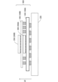
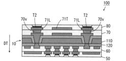
- FIG. 1 is a vertical cross-sectional view of a rewiring board according to an embodiment of the present invention.
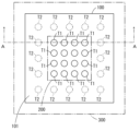
- FIG. 2 is a plan view of the rewiring board of FIG.
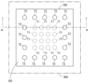
- FIG. 3 is a bottom view of the rewiring board of FIG.
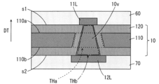
- FIG. 4 is an enlarged vertical cross-sectional view of a portion of the rewiring board of FIG.
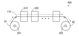
- FIG. 5 is a schematic side view showing an example of a roll-to-roll apparatus 500 used in the manufacturing process of a rewiring substrate.
- FIG. 6 is a schematic cross-sectional view for explaining an example of a method for manufacturing the rewiring board of FIG.
- FIG. 7 is a schematic cross-sectional view for explaining an example of a method for manufacturing the rewiring board of FIG. FIG.
- FIG. 8 is a schematic cross-sectional view for explaining an example of a method for manufacturing the rewiring board of FIG.
- FIG. 9 is a schematic cross-sectional view for explaining an example of a method for manufacturing the rewiring board of FIG.
- FIG. 10 is a schematic cross-sectional view for explaining an example of a method for manufacturing the rewiring board of FIG.
- FIG. 11 is a schematic cross-sectional view for explaining an example of a method for manufacturing the rewiring board of FIG.
- FIG. 12 is a schematic cross-sectional view for explaining an example of a method for manufacturing the rewiring board of FIG.
- FIG. 13 is a schematic cross-sectional view for explaining an example of a method for manufacturing the rewiring board of FIG. FIG.
- FIG. 14 is a schematic cross-sectional view for explaining an example of a method for manufacturing the rewiring board of FIG.
- FIG. 15 is a schematic cross-sectional view for explaining an example of a method for manufacturing the rewiring board of FIG.
- FIG. 16 is a diagram showing an application example of the rewiring board of FIG.
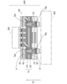
- FIG. 17 is a vertical cross-sectional view of a rewiring board according to another embodiment.
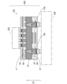
- FIG. 18 is a vertical cross-sectional view of a rewiring board according to still another embodiment.
- FIG. 19 is a vertical cross-sectional view of a rewiring board according to still another embodiment.
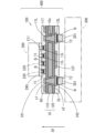
- FIG. 20 is a vertical cross-sectional view of a rewiring board according to still another embodiment.
- FIG. 21 is a schematic cross-sectional view for explaining an example of a method for manufacturing a rewiring substrate according to another embodiment.
- FIG. 22 is a schematic cross-sectional view for explaining an example of a method for manufacturing a rewiring substrate according to another embodiment.
- FIG. 23 is a schematic cross-sectional view for explaining an example of a method for manufacturing a rewiring substrate according to another embodiment.
- FIG. 24 is a schematic cross-sectional view for explaining an example of a method for manufacturing a rewiring substrate according to another embodiment.
- FIG. 25 is a schematic cross-sectional view for explaining an example of a method for manufacturing a rewiring substrate according to another embodiment.
- FIG. 22 is a schematic cross-sectional view for explaining an example of a method for manufacturing a rewiring substrate according to another embodiment.
- FIG. 23 is a schematic cross-sectional view for explaining an example of a method for manufacturing a rewiring substrate according to another embodiment.
- FIG. 26 is a schematic cross-sectional view for explaining an example of a method for manufacturing a rewiring substrate according to another embodiment.
- FIG. 27 is a schematic cross-sectional view for explaining an example of a method for manufacturing a rewiring substrate according to another embodiment.
- FIG. 28 is a schematic cross-sectional view for explaining an example of a method for manufacturing a rewiring substrate according to another embodiment.
- FIG. 29 is a schematic cross-sectional view for explaining an example of a method for manufacturing a rewiring substrate according to another embodiment.
- FIG. 30 is a schematic cross-sectional view for explaining an example of a method for manufacturing a rewiring substrate according to another embodiment.
- FIG. 31 is a schematic cross-sectional view for explaining an example of a method for manufacturing a rewiring substrate according to another embodiment.
- FIG. 32 is a schematic cross-sectional view for explaining an example of a method for manufacturing a rewiring substrate according to another embodiment.
- FIG. 33 is a schematic cross-sectional view for explaining an example of a method for manufacturing a rewiring substrate according to another embodiment.
- a rewired board will be described as an example of a wired circuit board.
- a rewired board is disposed between an electronic component such as a semiconductor element and another wired circuit board such as a rigid printed wiring circuit board (hereinafter abbreviated as a rigid board), and serves to convert the pitch between the fine patterns of the electronic components and the coarse patterns of the other wired circuit board.
- a rewired board is also called an interposer board.
- FIG. 1 is a vertical cross-sectional view of a redistribution substrate according to an embodiment of the present invention.
- FIG. 2 is a plan view of the redistribution substrate 100 of FIG. 1.
- FIG. 3 is a bottom view of the redistribution substrate 100 of FIG. 1.
- FIG. 4 is a partially enlarged vertical cross-sectional view of the redistribution substrate 100 of FIG. 1.
- FIG. 1 shows a cross section taken along line A-A in FIG. 2 and FIG. 3.
- the redistribution substrate 100 has a first surface (upper surface in this example) 101 and a second surface (lower surface in this example) 102 which face in opposite directions in the thickness direction DT of the redistribution substrate 100.
- the thickness direction DT of the redistribution substrate 100 is indicated by an arrow pointing from bottom to top.
- the rewiring substrate 100 is disposed between the semiconductor element 200 and the rigid substrate 300 in the thickness direction DT.
- a plurality of terminals T1 are formed on the first surface 101.
- the plurality of terminals T1 have a circular shape and a common maximum dimension (diameter) in a plan view.
- the diameter of the terminals T1 is, for example, 20 ⁇ m or more and 100 ⁇ m or less, preferably 30 ⁇ m or more and 70 ⁇ m or less, and more preferably 40 ⁇ m or more and 60 ⁇ m or less.
- the semiconductor element 200 has an opposing surface 211 that faces the rewiring substrate 100 when mounted on the rewiring substrate 100.
- the semiconductor element 200 also has a plurality of columnar joints 220 formed to protrude a certain length from the opposing surface 211.
- the tip of the columnar joint 220 constitutes a connection terminal of the semiconductor element 200 and is joined to the terminal T1 of the rewiring substrate 100 that is previously associated with it via solder S.
- Underfill 290 is filled between the opposing surface 211 of the semiconductor element 200 and the first surface 101 of the rewiring substrate 100.
- the underfill 290 is formed of, for example, epoxy resin.
- a lid member (not shown) that covers the semiconductor element 200 may be provided on the first surface 101 of the rewiring substrate 100.
- the semiconductor element 200 is indicated by a dashed line.
- a plurality of terminal portions T2 are formed on the second surface 102 of the rewiring substrate 100.
- the plurality of terminal portions T2 have a circular shape and a common maximum dimension (diameter) in a plan view.
- the diameter of the terminal portion T2 is larger than the diameter of the terminal portion T1, for example, 100 ⁇ m to 300 ⁇ m, preferably 170 ⁇ m to 250 ⁇ m, and more preferably 175 ⁇ m to 230 ⁇ m.
- the rigid substrate 300 has a plurality of electrode pads 301 as a plurality of connection terminals of the rigid substrate 300.
- the electrode pads 301 are joined to the terminal portions T2 of the rewiring substrate 100 to which they are previously associated via solder S. In FIGS.
- the rigid substrate 300 is indicated by a two-dot chain line.
- the semiconductor element mounting substrate 400 is incorporated into the electronic device 800, for example, by being mounted on the rigid substrate 300.
- the electronic device 800 is, for example, a mobile terminal such as a smartphone, a tablet terminal, or a wearable terminal.
- the electronic device 800 is, for example, a desktop or notebook personal computer.
- solder balls are provided on the multiple terminal portions T2 of the rewiring substrate 100.
- a BGA ball grid array
- the rewiring substrate 100 is mainly composed of one support layer 10, multiple insulating layers, and multiple conductor layers.
- the support layer 10 has higher rigidity than the multiple insulating layers.
- the support layer 10 is located approximately in the center of the rewiring substrate 100 in the thickness direction DT, and has a third surface s1 and a fourth surface s2 that face in opposite directions in the thickness direction DT.
- the third surface s1 faces the first surface 101
- the fourth surface s2 faces the second surface 102.
- the support layer 10 in this embodiment specifically includes a metal support 110 and an insulating coating layer 120, and the outer surface of the metal support 110 is covered with the insulating coating layer 120.
- the metal support 110 has a fifth surface 110a and a sixth surface 110b that face in opposite directions in the thickness direction DT.
- the fifth surface 110a faces the first surface 101 (FIG. 1)
- the sixth surface 110b faces the second surface 102 (FIG. 1).
- a plurality of through holes THa are formed in the metal support 110 (see the dotted arrows in FIG. 4).
- Each through hole THa has a circular shape in a plan view.
- the inner surface of the through hole THa is tapered such that the opening cross section perpendicular to the thickness direction DT gradually becomes smaller from the sixth surface 110b toward the fifth surface 110a.
- the inner diameter of the through hole THa from the sixth surface 110b to the fifth surface 110a is in the range of 10 ⁇ m to 80 ⁇ m, preferably in the range of 20 ⁇ m to 70 ⁇ m, and more preferably in the range of 30 ⁇ m to 60 ⁇ m.
- the metal support 110 is formed of, for example, stainless steel. Instead of stainless steel, the metal support 110 may be formed of copper, a copper alloy, aluminum, titanium, or an alloy containing iron and nickel. Examples of alloys containing iron and nickel include Invar, 42 alloy, 45 permalloy, and copper.
- the thickness of the metal support 110 is 10 ⁇ m or more and 100 ⁇ m or less, and preferably 20 ⁇ m or more and 60 ⁇ m or less.
- the insulating coating layer 120 is formed to cover the fifth surface 110a, the sixth surface 110b, and the inner surface of the through hole THa of the metal support 110.
- through holes THb are formed so as to pass through the portions of the metal support 110 where the through holes THa are formed in the thickness direction DT (see the dashed arrows in FIG. 4).
- Each through hole THb has a circular shape in a plan view.
- the inner surface of the through hole THb is formed in a tapered shape in which the opening cross section perpendicular to the thickness direction DT gradually becomes smaller from the fourth surface s2 to the third surface s1.
- the inner diameter of the through hole THb is in the range of 5 ⁇ m to 85 ⁇ m from the fourth surface s2 to the third surface s1, preferably in the range of 15 ⁇ m to 75 ⁇ m, and more preferably in the range of 25 ⁇ m to 65 ⁇ m.
- the insulating coating layer 120 is formed, for example, from photosensitive polyimide and has a thickness of 1 ⁇ m to 25 ⁇ m, preferably 3 ⁇ m to 20 ⁇ m.
- the insulating coating layer 120 may be formed from other photosensitive materials instead of photosensitive polyimide. Examples of such other photosensitive materials include photosensitive resins such as acrylic resin, epoxy resin, polyamide resin, polybenzoxazole resin, and polyvinyl chloride resin. Materials other than photosensitive materials may be used as the material of the insulating coating layer 120.
- inorganic insulating materials or organic insulating materials may be used as the material of the insulating coating layer 120. Specifically, silicon carbide, silicon dioxide, aluminum nitride, aluminum oxide, etc. may be used as the material of the insulating coating layer 120.
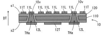
- a via conductor portion 10v made of a conductive material is formed inside the through hole THb of the support layer 10 so as to extend in the thickness direction DT.
- a land portion 11L made of a conductive material is formed on the third surface s1 of the support layer 10 so as to cover the end portion of the via conductor portion 10v on the third surface s1 side.
- the land portion 11L has a circular shape in a plan view.
- the outer diameter of the land portion 11L is approximately 30 ⁇ m larger than the inner diameter of the opening of the through hole THb on the third surface s1.
- the land portion 11L is designed to cover an area of approximately 15 ⁇ m from the inner edge of the through hole THb on the third surface s1.
- a land portion 12L made of a conductive material is formed on the fourth surface s2 of the support layer 10 so as to cover the end of the via conductor portion 10v on the fourth surface s2 side.
- the land portion 12L has a circular shape in a plan view.
- the outer diameter of the land portion 12L is approximately 30 ⁇ m larger than the inner diameter of the opening of the through hole THb on the fourth surface s2.
- the land portion 12L is designed to cover an area of approximately 15 ⁇ m from the inner edge of the through hole THb on the fourth surface s2.
- the land portion 11L that covers the smallest diameter portion of the through hole THb is smaller than the land portion 12L that covers the largest diameter portion of the through hole THb.
- the above-mentioned via conductor portion 10v and the land portions 11L and 12L are part of multiple conductor layers.
- the rewiring substrate 100 of FIG. 1 includes four insulating layers. Two of the four insulating layers are laminated on the third surface s1 of the support layer 10. The remaining two of the four insulating layers are laminated on the fourth surface s2 of the support layer 10.
- the four insulating layers are called the first insulating layer 50, the second insulating layer 60, the third insulating layer 70, and the fourth insulating layer 80, respectively.
- the second insulating layer 60 and the first insulating layer 50 are laminated in this order on the third surface s1 of the support layer 10.
- the third insulating layer 70 and the fourth insulating layer 80 are laminated in this order on the fourth surface s2 of the support layer 10.
- Each of the four insulating layers (50, 60, 70, 80) is formed of a photosensitive material.
- photosensitive polyimide is used as the photosensitive material used for the four insulating layers (50, 60, 70, 80).
- the insulating layers (50, 60, 70, 80) may be formed of other photosensitive resins (acrylic resin, epoxy resin, polyamide resin, polybenzoxazole resin, polyvinyl chloride resin, or other photosensitive resins) instead of photosensitive polyimide.
- each of the insulating layers (50, 60, 70, 80) on the conductor is 2 ⁇ m or more and 25 ⁇ m or less, preferably 4 ⁇ m or more and 20 ⁇ m or less, and more preferably 5 ⁇ m or more and 10 ⁇ m or less.
- the multiple conductor layers include the multiple via conductors 10v and multiple land portions 11L, 12L described above, as well as multiple via conductors 60v, 70v, multiple land portions 61L, 71L, and multiple wiring portions 11T, 12T, 61T, 71T.
- the wiring portion 11T is formed on the third surface s1 of the support layer 10 together with a plurality of land portions 11L.
- the second insulating layer 60 is formed on the third surface s1 of the support layer 10 so as to cover the plurality of land portions 11L and the wiring portion 11T.
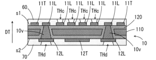
- the second insulating layer 60 has a plurality of through holes THc (see FIG. 12 described later) extending in the thickness direction DT formed as via holes. Via conductor portions 60v are formed in the plurality of through holes THc.
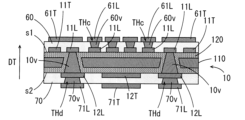
- the land portions 61L are formed on the second insulating layer 60 so as to cover the via conductor portions 60v.
- the wiring portion 61T is formed on the second insulating layer 60 together with the land portions 61L.
- the first insulating layer 50 is formed on the second insulating layer 60 so as to cover the land portions 61L and the wiring portion 61T.
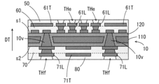
- the first insulating layer 50 has a plurality of through holes THe (see FIG. 14 described later) for exposing each of the land portions 61L on the first surface 101 of the rewiring substrate 100.
- a terminal portion T1 is formed in each through hole THe.
- the terminal portion T1 may be formed of a part of the land portion 61L, or may be formed by subjecting a part of the land portion 61L to a surface treatment.
- the terminal portion T1 may be formed by subjecting a part of the land portion 61L to an anti-rust treatment.
- the terminal portion T1 may be formed by growing a plating layer of a metal having excellent corrosion resistance, such as gold, on a part of the land portion 61L.
- Each of the multiple land portions 11L, 61L and wiring portions 11T, 61T formed between the first surface 101 and the support layer 10 in the above-mentioned rewiring substrate 100 is electrically connected, directly or indirectly, to one of the multiple terminal portions T1. Also, each of the multiple land portions 11L, 61L and multiple wiring portions 11T, 61T is electrically connected, directly or indirectly, to one of the multiple via conductor portions 10v.
- the wiring portion 12T is formed on the fourth surface s2 of the support layer 10 together with the multiple land portions 12L.
- the third insulating layer 70 is formed on the fourth surface s2 of the support layer 10 so as to cover the multiple land portions 12L and the wiring portion 12T.
- the third insulating layer 70 has multiple through holes THd (see FIG. 12 described later) extending in the thickness direction DT formed as via holes. Via conductor portions 70v are formed in the multiple through holes THd.
- the plurality of land portions 71L are formed on the third insulating layer 70 so as to cover the plurality of via conductor portions 70v.
- the plurality of wiring portions 71T are formed on the third insulating layer 70 together with the plurality of land portions 71L.
- the fourth insulating layer 80 is formed on the third insulating layer 70 so as to cover the plurality of land portions 71L and the wiring portion 71T.
- the fourth insulating layer 80 is formed with a plurality of through holes THf (see FIG. 14 described later) for exposing each of the plurality of land portions 71L on the second surface 102 of the rewiring substrate 100.
- a terminal portion T2 is formed in each through hole THf.
- the terminal portion T2 may be formed of a part of the land portion 71L, or may be formed by subjecting a part of the land portion 71L to a surface treatment.
- the terminal portion T2 may be formed by subjecting a part of the land portion 71L to an anti-rust treatment.
- the terminal portion T2 may be formed by growing a plating layer of a metal having excellent corrosion resistance, such as gold, on a part of the land portion 71L.
- Each of the multiple land portions 12L, 71L and wiring portions 12T, 71T formed between the second surface 102 and the support layer 10 in the above-mentioned rewiring substrate 100 is electrically connected directly or indirectly to one of the multiple terminal portions T2. Also, each of the multiple land portions 12L, 71L and multiple wiring portions 12T, 71T is electrically connected directly or indirectly to one of the multiple via conductor portions 10v.
- Each of the multiple conductor layers is basically formed by growing a plating layer on a seed layer by electrolytic plating.
- the seed layer forming the conductor layer is, for example, made of a chromium thin film and a copper thin film.
- the seed layer is made of a copper thin film.
- the seed layer may contain either nickel or palladium.
- the plating layer is formed of a metal or alloy containing one or more of copper, gold, silver, platinum, lead, tin, nickel, cobalt, indium, rhodium, chromium, tungsten, and ruthenium. In this embodiment, the plating layer is copper.
- each of the above-mentioned land portions 11L, 61L and wiring portions 11T, 61T is 20 ⁇ m or more and 120 ⁇ m or less, preferably 40 ⁇ m or more and 100 ⁇ m or less, and more preferably 60 ⁇ m or more and 80 ⁇ m or less. Furthermore, the thickness of each of the above-mentioned land portions 12L, 71L and wiring portions 12T, 71T is 20 ⁇ m or more and 300 ⁇ m or less, preferably 50 ⁇ m or more and 250 ⁇ m or less, and more preferably 70 ⁇ m or more and 200 ⁇ m or less.
- the number of the multiple terminal portions T1 located on the first surface 101 of the redistribution substrate 100 is equal to the number of the multiple terminal portions T2 located on the second surface 102 of the redistribution substrate 100, but the present invention is not limited to this.
- the number of the multiple terminal portions T1 located on the first surface 101 of the redistribution substrate 100 does not have to be equal to the number of the multiple terminal portions T2 located on the second surface 102 of the redistribution substrate 100.
- the redistribution substrate 100 is manufactured by, for example, a roll-to-roll method.
- Fig. 5 is a schematic side view showing an example of a roll-to-roll apparatus 500 used in the manufacturing process of the redistribution substrate 100.
- the roll-to-roll device 500 includes an unwinding section 501, a winding section 502, and a number of processing sections 510, 520, ....
- a roll (unwinding roll) R1 on which the long metal support 110 is wound is prepared and set in the unwinding section 501 of the roll-to-roll device 500.
- the metal support 110 is unwound from a prepared unwinding roll R1.
- the unwound metal support 110 is then wound onto another roll (winding roll) R2 set in the winding section 502, as shown by the dotted arrow in FIG. 5.
- multiple processing sections 510, 520, ... are arranged between two rolls (R1, R2) in the direction of movement of the metal support 110.
- the multiple processing sections 510, 520, ... form an insulating coating layer 120 on the long metal support 110 moving between the two rolls (R1, R2).
- the multiple insulating layers and multiple conductor layers, etc. are formed in each area of the metal support 110 on which the insulating coating layer 120 is formed.
- multiple rewiring substrates 100 are formed on the metal support 110 that is wound up on the winding roll R2.
- the manufacturing method for the rewiring substrate 100 is described in detail below.
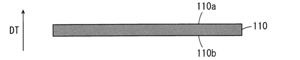
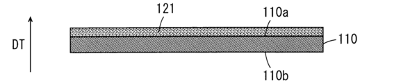
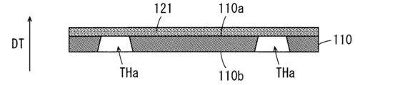
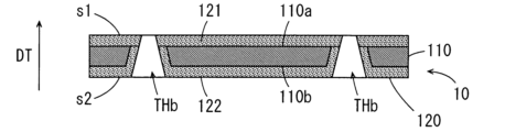
- FIGS. 6 to 15 are schematic cross-sectional views for explaining an example of a method for manufacturing the redistribution substrate 100 of FIG. 1.
- the schematic cross-sectional views shown in FIG. 6 to FIG. 15 correspond to the schematic cross-sectional view of the redistribution substrate 100 of FIG. 1.
- Each of FIG. 6 to FIG. 15 shows the thickness direction DT of FIG. 1.
- FIG. 5 shows a cross section of a portion of the paid-out metal support 110.
- the metal support 110 has a fifth surface 110a and a sixth surface 110b that face in opposite directions in the thickness direction DT.
- a photosensitive polyimide precursor is applied to one surface (fifth surface 110a in this example) of the metal support 110 so as to cover the entire fifth surface 110a.
- the applied photosensitive polyimide precursor is exposed to light and developed.
- a first temporary coating layer 121 is formed on the fifth surface 110a of the metal support 110.
- the formed first temporary coating layer 121 is subjected to a curing process.
- the first temporary coating layer 121 may be formed by attaching a film made of photosensitive polyimide instead of applying a photosensitive polyimide precursor to the fifth surface 110a.
- an etching resist having a predetermined pattern is formed on the other surface (sixth surface 110b in this example) of the metal support 110. Furthermore, the portions of the sixth surface 110b of the metal support 110 that are exposed through the openings in the etching resist are etched, and a plurality of through holes THa are formed in the metal support 110. Thereafter, the etching resist is peeled off from the metal support 110.
- each through hole THa is formed so that the inner diameter gradually decreases from the sixth surface 110b toward the fifth surface 110a.
- the etching solution used to etch the metal support 110 does not dissolve the first temporary coating layer 121. Therefore, one end of each through hole THa is blocked by the first temporary coating layer 121.
- the multiple through holes THa in the metal support 110 may be formed by, for example, laser processing, rather than by etching.
- the metal support 110 is irradiated with laser light so as to travel from the sixth surface 110b toward the fifth surface 110a, without penetrating the first temporary coating layer 121.
- each through hole THa is formed so that the inner diameter gradually decreases from the sixth surface 110b toward the fifth surface 110a. Also, one end of each through hole THa is blocked by the first temporary coating layer 121.
- a photosensitive polyimide precursor is applied to the other surface (sixth surface 110b in this example) of the metal support 110 so as to cover the entire surface and to penetrate into each through hole THa.
- the applied photosensitive polyimide precursor is exposed to light and developed.
- a second temporary coating layer 122 is formed so as to cover the sixth surface 110b of the metal support 110 and the inner surfaces of the multiple through holes THa and to fill the multiple through holes THa.
- the formed second temporary coating layer 122 is subjected to a curing process.
- the second temporary coating layer 122 may be formed by attaching a film made of photosensitive polyimide instead of applying a photosensitive polyimide precursor to the sixth surface 110b.
- a plurality of through holes THb are formed in a plurality of portions of the metal support 110 so as to extend in the thickness direction DT through the interior of each through hole THa of the metal support 110.
- These through holes THb are formed, for example, by etching or laser processing.
- the etching or laser processing is performed so that a hole is formed from the sixth surface 110b toward the fifth surface 110a.
- each through hole THb is formed so that the inner diameter gradually becomes smaller from the sixth surface 110b toward the fifth surface 110a. In this way, the support layer 10 is completed.
- a seed layer is formed on a predetermined region of the third surface s1 of the support layer 10, a predetermined region of the fourth surface s2 of the support layer 10, and the inner surface of the through hole THb, and a plating layer is formed on the seed layer.
- a plurality of land portions 11L and a plurality of wiring portions 11T are formed on the third surface s1 of the support layer 10.
- a plurality of land portions 12L and a plurality of wiring portions 12T are formed on the fourth surface s2 of the support layer 10.
- a plurality of via conductor portions 10v are formed inside the plurality of through holes THa of the support layer 10.
- a second insulating layer 60 is formed on the third surface s1 of the support layer 10 so as to cover the multiple land portions 11L and the multiple wiring portions 11T.
- a multiple number of through holes THc are formed in the second insulating layer 60 so that some of the multiple land portions 11L are exposed on the second insulating layer 60.
- a third insulating layer 70 is formed on the fourth surface s2 of the support layer 10 so as to cover the multiple land portions 12L and the wiring portions 12T.
- a multiple number of through holes THd are formed in the third insulating layer 70 so that some of the multiple land portions 12L are exposed on the third insulating layer 70.
- a seed layer is formed on a predetermined region of the exposed surface of the second insulating layer 60 and a predetermined region of the exposed surface of the third insulating layer 70.
- a seed layer is also formed on the inner circumferential surfaces of the through holes THc, THd and the exposed portions of the land portions 11L, 12L.
- a plating layer is formed on the formed seed layer.
- a plurality of land portions 61L and a plurality of wiring portions 61T are formed on the second insulating layer 60.
- a plurality of land portions 71L and a plurality of wiring portions 71T are formed on the third insulating layer 70.
- a plurality of via conductor portions 60v are formed inside the plurality of through holes THc of the second insulating layer 60, and a plurality of via conductor portions 70v are formed inside the plurality of through holes THd of the third insulating layer 70.
- a first insulating layer 50 is formed on the second insulating layer 60 so as to cover the multiple land portions 61L and the multiple wiring portions 61T.
- a multiple number of through holes THe are formed in the first insulating layer 50 so that some of the multiple land portions 61L are exposed on the first insulating layer 50.
- a fourth insulating layer 80 is formed on the third insulating layer 70 so as to cover the multiple land portions 71L and the wiring portions 71T.
- a multiple number of through holes THf are formed in the fourth insulating layer 80 so that some of the multiple land portions 71L are exposed on the fourth insulating layer 80.
- terminal portions T1 are formed on the portions of the land portions 61L that are exposed through the through holes THe.
- Terminal portions T2 are formed on the portions of the land portions 71L that are exposed through the through holes THf. This completes the rewiring substrate 100 of FIG. 1.
- the support layer 10 has higher rigidity than the insulating layers (50, 60, 70, 80). As a result, the rewiring substrate 100 has higher handleability than a substrate not including the support layer 10.
- each through hole THb formed in the support layer 10 is tapered so that the opening cross section perpendicular to the thickness direction DT gradually becomes smaller from the fourth surface s2 toward the third surface s1.
- the opening area of the through hole THb on the third surface s1 of the support layer 10 is smaller than the opening area of the through hole THb on the fourth surface s2.
- the land portion 11L formed on the third surface s1 of the support layer 10 is smaller than the land portion 12L formed on the fourth surface s2.
- the land portions 11L and 12L located at both ends of the via conductor portion 10v in the thickness direction DT are formed according to the opening area of the through hole THb.
- the reliability of the electrical connection between the via conductor portion 10v and one of the land portions 11L is ensured, and the reliability of the electrical connection between the via conductor portion 10v and the other land portion 12L is ensured.
- the portion of the rewiring substrate 100 located closer to the first surface 101 than the support layer 10 is referred to as the first substrate portion.
- the portion of the rewiring substrate 100 located closer to the second surface 102 than the support layer 10 is referred to as the second substrate portion.
- the land portion 11L formed on the first substrate portion is smaller than the land portion 12L formed on the second substrate portion.
- the terminal portion T1 formed on the first substrate portion is smaller than the terminal portion T2 formed on the second substrate portion.
- the area required to form the land portion 11L and the terminal portion T1 on the first substrate portion can be reduced compared to the area required to form the land portion 12L and the terminal portion T2 on the second substrate portion.
- the second substrate portion can be connected to a rigid substrate 300, which does not require a high wiring density.
- a rewiring substrate 100 is realized that has high reliability of electrical connection and increased freedom of wiring design. Therefore, the semiconductor element mounting substrate 400 and electronic device 800 that include the rewiring substrate 100 described above have high reliability.
- the support layer 10 includes a metal support 110. This makes it easier for the support layer 10 to ensure the rigidity required for the rewiring substrate 100.
- each through hole THb formed in the support layer 10 is tapered so that the opening cross section perpendicular to the thickness direction DT gradually becomes smaller from the fourth surface s2 toward the third surface s1. Furthermore, in the support layer 10, each through hole THa of the metal support 110 covered by the insulating coating layer 120 is also tapered so that the opening cross section perpendicular to the thickness direction DT gradually becomes smaller from the fourth surface s2 toward the third surface s1.
- the shape of the inner circumferential surface of the through hole THb formed by the insulating coating layer 120 and the shape of the inner circumferential surface of the through hole THa formed by the metal support 110 roughly match.
- the portion of the insulating coating layer 120 that forms the inner circumferential surface of the through hole THb is appropriately reinforced by the inner circumferential surface of the through hole THa of the metal support 110. Therefore, the mechanical strength of the through hole THb and the surrounding area in the support layer 10 is improved, and the reliability of the electrical conduction in the via conductor portion 10v is improved.
- FIG. 16 is a diagram showing an application example of the redistribution substrate 100 of FIG. 1.
- FIG. 16 an example is shown in which the redistribution substrate 100 of FIG. 1 is applied to a stacked semiconductor device.
- the semiconductor device 900 of FIG. 16 is an example of a semiconductor element mounting substrate, and includes two redistribution substrates 100 and two semiconductor elements 200, and is mounted on a rigid substrate 300.
- one redistribution substrate 100 is called the first redistribution substrate 100A
- the other redistribution substrate 100 is called the second redistribution substrate 100B
- one semiconductor element 200 is called the first semiconductor element 200A
- the other semiconductor element 200 is called the second semiconductor element 200B.
- a first semiconductor element 200A is mounted on a first redistribution substrate 100A by flip chip bonding.
- a second redistribution substrate 100B is stacked on the first redistribution substrate 100A so as to cover the first semiconductor element 200A.
- a second semiconductor element 200B is mounted on the second redistribution substrate 100B by flip chip bonding.
- electrical continuity between the multiple wirings is ensured by using multiple solder balls.
- electrical continuity between the multiple wirings is ensured by using multiple solder balls.
- the first semiconductor element 200A exchanges electrical signals with the second semiconductor element 200B mounted on the second rewiring substrate 100B, and also exchanges electrical signals with other electronic components mounted on the rigid substrate 300. Therefore, on the side of the first rewiring substrate 100A on which the first semiconductor element 200A is mounted, a large number of wires are required for the first semiconductor element 200A to exchange electrical signals with the second semiconductor element 200B and other electronic devices on the rigid substrate 300.
- the rewiring substrate 100 of FIG. 1 can have a high wiring density on the first surface 101 side. Therefore, the first semiconductor element 200A is mounted on the first surface 101, and the second rewiring substrate 100B is stacked. This makes it possible to ensure a highly reliable wiring structure for the first semiconductor element 200A while preventing the substrate from becoming too large. In this way, the rewiring substrate 100 of FIG. 1 can be effectively used in a configuration that utilizes package-on-package technology.
- FIG. 17 is a longitudinal sectional view of a rewiring substrate 100 according to another embodiment. Regarding the rewiring substrate 100 in Fig. 17, differences from the rewiring substrate 100 in Fig. 1 will be described.
- the through holes THa of the metal support 110 are not tapered.
- each of the through holes THa of the metal support 110 has a constant inner diameter from the fourth surface s2 to the third surface s1.
- the through holes THb (through holes THb of the support layer 10) formed in the insulating coating layer 120 are tapered such that the opening cross section perpendicular to the thickness direction DT gradually becomes smaller from the fourth surface s2 to the third surface s1. This makes it possible to ensure a reliable electrical connection between the multiple conductor layers and to increase the freedom of wiring design, as with the rewiring substrate 100 according to the above embodiment.
- Figure 18 is a vertical cross-sectional view of a rewiring substrate 100 according to yet another embodiment.
- the rewiring substrate 100 in Figure 18 is different from the rewiring substrate 100 in Figure 1.
- the through hole THb is formed so as to be partially constricted, as indicated by the hollow arrow. Even in such a case, it is sufficient that the inner diameter of the opening of the through hole THb on the third surface s1 is smaller than the inner diameter of the opening of the through hole THb on the fourth surface s2. This makes it possible to ensure a highly reliable electrical connection between multiple conductor layers and to increase the freedom of wiring design, similar to the rewiring substrate 100 according to the above embodiment.
- Figure 19 is a vertical cross-sectional view of a rewiring substrate 100 according to yet another embodiment.
- the rewiring substrate 100 in Figure 19 will be described in terms of differences from the rewiring substrate 100 in Figure 1.
- the support layer 10 only needs to have a higher rigidity than the multiple insulating layers (50, 60, 70, 80). Therefore, in the rewiring substrate 100 of FIG. 19, a single member that does not include the metal support 110 of FIG. 1 is used as the support layer 10.
- Materials that can be used for the support layer 10 in this example include, for example, organic materials, inorganic materials, organic-inorganic hybrid materials, or composite materials that have a higher rigidity than the multiple insulating layers (50, 60, 70, 80).
- polyimide or the like can be used as the organic material.
- ceramics such as glass can be used as the inorganic material.
- materials composed of epoxy resin and silica filler, or materials composed of epoxy resin and glass fiber can be used as the organic-inorganic hybrid material and composite material.
- the support layer 10 can be made of a material (FR4) made by impregnating a cloth made of glass fiber with epoxy resin and hardening it. In this case, the process of covering the metal support 110 with the insulating coating layer 120 is not necessary. Alternatively, it is possible to use a ready-made product. This simplifies the manufacturing process of the support layer 10.
- FR4 a material made by impregnating a cloth made of glass fiber with epoxy resin and hardening it.
- Figure 20 is a vertical cross-sectional view of a rewiring substrate 100 according to yet another embodiment.
- the rewiring substrate 100 in Figure 20 is different from the rewiring substrate 100 in Figure 1.
- the second insulating layer 60 is formed on the third surface s1 of the support layer 10, but the first insulating layer 50 of FIG. 1 is not formed on the second insulating layer 60.
- the third insulating layer 70 is formed on the fourth surface s2 of the support layer 10, but the fourth insulating layer 80 of FIG. 1 is not formed on the third insulating layer 70. Therefore, in the first substrate portion of the rewiring substrate 100 on the first surface 101 side of the support layer 10, multiple conductor layers (land portion 11L and wiring portion 11T) are formed in a single surface.
- the second substrate portion of the rewiring substrate 100 on the second surface 102 side of the support layer 10 multiple conductor layers (land portion 12L and wiring portion 12T) are formed in a single surface. Even in such a configuration, the density of the wiring portion 11T formed in the first substrate portion can be increased.
- the rewiring substrate 100 according to the above embodiment is not limited to the examples shown in FIGS. 6 to 15, and may be manufactured by the following method. Note that in the manufacturing method of the rewiring substrate 100 described below, the rewiring substrate 100 is also manufactured by, for example, a roll-to-roll method.
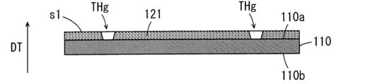
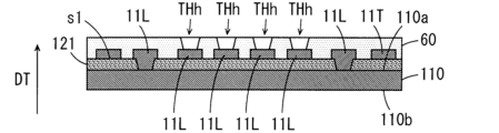
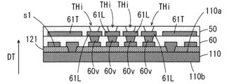
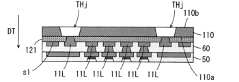
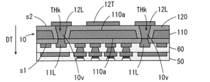
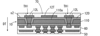
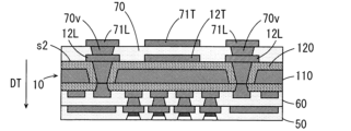
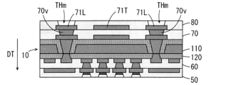
- FIGS. 21 to 33 are schematic cross-sectional views for explaining an example of a manufacturing method for a redistribution substrate 100 according to another embodiment.
- the schematic cross-sectional views shown in FIG. 21 to FIG. 33 correspond to the schematic cross-sectional view of the redistribution substrate 100 in FIG. 1, as in the examples of FIG. 6 to FIG. 15.
- Each of FIG. 21 to FIG. 33 shows the thickness direction DT in FIG. 1.
- the direction of the arrow in the thickness direction DT in FIG. 21 to FIG. 33 is the direction from the rigid substrate 300 to the semiconductor element 200 when the redistribution substrate 100 is disposed between the semiconductor element 200 and the rigid substrate 300.
- the metal support 110 of FIG. 6 having a fifth surface 110a and a sixth surface 110b is prepared.
- a first temporary coating layer 121 is formed on the fifth surface 110a of the metal support 110.
- one or more (two in this example) through holes THg are formed in the first temporary coating layer 121.
- the exposed surface of the first temporary coating layer 121 becomes the third surface s1 of the support layer 10.
- the first temporary coating layer 121 is formed by applying a precursor of photosensitive polyimide or by attaching a film made of photosensitive polyimide onto the fifth surface 110a.
- One or more through holes THg may be formed by exposing the photosensitive polyimide using a specific photomask and developing it, or by etching or laser processing a part of the first temporary coating layer 121 that has been hardened.
- a seed layer is formed on a predetermined region of the third surface s1 and on the inner surface of the through hole THg, and a plating layer is formed on the seed layer.
- a plurality of land portions 11L and a plurality of wiring portions 11T are formed on the third surface s1.
- a plurality of via conductor portions are formed inside the plurality of through holes THg of the first temporary coating layer 121.
- a second insulating layer 60 is formed on the third surface s1 so as to cover the multiple land portions 11L and the multiple wiring portions 11T.
- multiple through holes THh are formed in the second insulating layer 60 so that some of the multiple land portions 11L are exposed on the second insulating layer 60.
- a seed layer is formed in a predetermined region of the exposed surface of the second insulating layer 60.
- a seed layer is also formed on the inner surfaces of the multiple through holes THh and the exposed portions of the multiple land portions 11L.
- a plating layer is formed on the formed seed layer.
- multiple land portions 61L and multiple wiring portions 61T are formed on the second insulating layer 60.
- multiple via conductor portions 60v are formed inside the multiple through holes THh of the second insulating layer 60. After the land portions 61L, wiring portions 61T and via conductor portions 60v are formed, the seed layer is removed.
- a first insulating layer 50 is formed on the second insulating layer 60 so as to cover the land portions 61L and the wiring portions 61T. Furthermore, a plurality of through holes THi are formed in the first insulating layer 50 so that some of the land portions 61L are exposed on the first insulating layer 50. Thereafter, as shown in FIG. 26, terminal portions T1 are formed on the portions of the land portions 61L exposed through the through holes THi.
- the portion of the rewiring substrate 100 located on the sixth surface 110b of the metal support 110 (the portion on the rigid substrate 300 side in FIG. 1) is fabricated.
- the orientation of the thickness direction DT in the schematic cross-sectional views is inverted vertically relative to the schematic cross-sectional views in FIGS. 22 to 26 so that it is easy to understand that the portion of the rewiring substrate 100 on the rigid substrate 300 side is being fabricated.
- a plurality of through holes THj are formed in a plurality of predetermined portions of the metal support 110.
- Each of the plurality of through holes THj exposes a portion of the via conductor portion formed inside the plurality of through holes THg (FIG. 21) of the first temporary coating layer 121 through the through hole THj on the sixth surface 110b of the metal support 110.
- each through hole THj is formed so that the inner diameter gradually decreases from the sixth surface 110b toward the fifth surface 110a.
- a second temporary coating layer 122 is formed on the sixth surface 110b of the metal support 110 so as to cover the entire sixth surface 110b of the metal support 110 and fill the multiple through holes THj. Further through holes THk are formed in the portions of the second temporary coating layer 122 in each through hole THj. This completes the insulating coating layer 120 that covers the fifth surface 110a, the sixth surface 110b of the metal support 110, and the inner surfaces of the through holes THj (FIG. 27) of the metal support 110, as shown in FIG. 28.
- the support layer 10 is formed by the metal support 110 and the insulating coating layer 120.
- the exposed surface of the second temporary coating layer 122 becomes the fourth surface s2 of the support layer 10.
- Inside each through hole THk a portion of the conductor layer (via conductor portion) formed in the through hole THg of the first temporary coating layer 121 is exposed.
- the method of forming the second temporary coating layer 122 and the method of forming the multiple through holes THk are basically the same as the method of forming the first temporary coating layer 121 and the method of forming the multiple through holes THg.
- a seed layer is formed on a predetermined region of the fourth surface s2, on the inner surfaces of the multiple through holes THk, and on the portions of the conductor layer (via conductor portion) exposed within each through hole THk, and a plating layer is formed on the seed layer.
- a seed layer is formed on a predetermined region of the fourth surface s2, on the inner surfaces of the multiple through holes THk, and on the portions of the conductor layer (via conductor portion) exposed within each through hole THk, and a plating layer is formed on the seed layer.
- multiple land portions 12L and wiring portions 12T are formed on the fourth surface s2.
- multiple via conductor portions 10v are formed inside the multiple through holes THk.
- a third insulating layer 70 is formed on the fourth surface s2 so as to cover the multiple land portions 12L and the wiring portion 12T.
- multiple through holes TH1 are formed in the third insulating layer 70 so that some of the multiple land portions 12L are exposed on the third insulating layer 70.
- a seed layer is formed in a predetermined region of the exposed surface of the third insulating layer 70.
- a seed layer is also formed on the inner circumferential surfaces of the multiple through holes TH1 and the exposed portions of the multiple land portions 12L.
- a plating layer is formed on the formed seed layer.
- multiple land portions 71L and wiring portions 71T are formed on the third insulating layer 70.
- multiple via conductor portions 70v are formed inside the multiple through holes TH1 of the third insulating layer 70. After the land portions 71L, wiring portions 71T and via conductor portions 70v are formed, the seed layer is removed.
- a fourth insulating layer 80 is formed on the third insulating layer 70 so as to cover the multiple land portions 71L and wiring portions 71T.
- multiple through holes THm are formed in the fourth insulating layer 80 so that some of the multiple land portions 71L are exposed on the fourth insulating layer 80.
- terminal portions T2 are formed on the portions of the multiple land portions 71L that are exposed through the multiple through holes THm. This completes the rewiring substrate 100 according to another embodiment.
- the method of forming the multiple insulating layers (50, 60, 70, 80) and the method of forming the multiple through holes (THi, THh, THl, THm) in each insulating layer are basically the same as the method of forming the first temporary coating layer 121 and the method of forming the multiple through holes THg.
- the part of the redistribution substrate 100 on the semiconductor element 200 side with respect to the metal support 110 as a reference, and the part of the redistribution substrate 100 on the rigid substrate 300 side with respect to the metal support 110 as a reference are formed separately. This makes it easier to adjust the positioning and processing conditions when forming each part, compared to when the part of the redistribution substrate 100 on the semiconductor element 200 side and the part on the rigid substrate 300 side are formed simultaneously. As a result, it becomes possible to form each part with high precision relative to the design dimensions. Furthermore, since complex processing is not required, there is no need to prepare expensive manufacturing equipment.
- a conductor layer including a land portion and a wiring portion and an insulating layer are alternately formed on the first temporary covering layer 121.
- the portion of the redistribution substrate 100 facing the semiconductor element 200 may be produced as follows.
- a dry film resist is laminated onto the third surface s1 without removing the seed layer used to form these conductor layers.
- the laminated dry film resist is then exposed to light in a desired pattern and developed to form openings of a predetermined pattern in the dry film resist.
- the predetermined pattern of the openings is determined so as to expose a portion of the multiple land portions 11L.
- the seed layer remaining on the third surface s1 is used to form an additional plating layer on the land portion 11L exposed through the opening in the dry film resist. After that, the dry film resist is removed, and the seed layer is removed.
- the additional plating layer protrudes a predetermined distance from the land portion 11L on which the plating layer is formed in the direction toward the third surface s1.
- the additional plating layer formed on the land portion 11L is called a plating protrusion.
- an insulating layer can be formed relatively easily on the third surface s1 in the area excluding the plating protrusion. Therefore, a second insulating layer 60 is formed on the third surface s1 to cover the area other than the plating protrusion. Alternatively, the second insulating layer 60 is formed on the entire third surface s1 including the plating protrusion, and then an opening is formed in the portion of the second insulating layer 60 that overlaps the plating protrusion. In these cases, a terminal portion T1 can be formed at the tip of the plating protrusion.
- each of the terminal portion T1 and the terminal portion T2 has a circular shape in a plan view, but the present invention is not limited to this.
- Each of the terminal portion T1 and the terminal portion T2 may have a shape other than a circle (an elliptical shape or a polygonal shape) in a plan view.
- the through holes THa and THb each have a circular shape in a planar view, but the present invention is not limited to this.
- the through holes THa and THb each may have a shape other than a circle (an ellipse or a polygon) in a planar view.
- the wiring portions 11T, 12T, 61T, and 71T are formed to correspond to each of the multiple insulating layers (50, 60, 70, and 80), but the present invention is not limited to this.
- the wiring portion may be formed to correspond to only some of the insulating layers (50, 60, 70, 80).
- the wiring portion 71T may not be provided.
- the wiring portion 12T may not be provided.
- the rewiring substrate 100 is manufactured by a roll-to-roll method, but the present invention is not limited to this.
- the rewiring substrate 100 may be manufactured by a method other than the roll-to-roll method. For example, it may be manufactured by a sheet-by-sheet method in which processing is performed sequentially on a single sheet.
- the redistribution substrate 100 is an example of a wiring circuit substrate
- the first surface 101 is an example of a first surface
- the second surface 102 is an example of a second surface
- the terminal portion T1 is an example of a first terminal
- the terminal portion T2 is an example of a second terminal
- the third surface s1 is an example of a third surface
- the fourth surface s2 is an example of a fourth surface.
- the support layer 10 is an example of a support layer
- the through hole THb is an example of a first through hole
- the first insulating layer 50 and the second insulating layer 60 are examples of a first insulating layer
- the third insulating layer 70 and the fourth insulating layer 80 are examples of a second insulating layer
- the land portions 11L, 61L and the wiring portions 11T, 61T are examples of a first conductor layer
- the land portions 12L, 71L and the wiring portions 12T, 71T are examples of a second conductor layer
- the via conductor portion 10v is an example of a third conductor layer.
- land portion 11L is an example of a first land portion
- land portion 12L is an example of a second land portion
- fifth surface 110a is an example of a fifth surface
- sixth surface 110b is an example of a sixth surface
- metal support 110 is an example of a metal support
- insulating coating layer 120 is an example of an insulating coating layer
- semiconductor element mounting board 400 and semiconductor device 900 are examples of electrical element mounting boards
- electronic device 800 is an example of an electronic device.
- the printed circuit board according to the first embodiment is A wired circuit board having a first surface and a second surface facing in opposite directions in a thickness direction, the wired circuit board including a first terminal formed on the first surface and a second terminal formed on the second surface and larger than the first terminal, a support layer provided between the first surface and the second surface, the support layer having a third surface facing the first surface and a fourth surface facing the second surface, and a first through hole penetrating from the third surface to the fourth surface; a first insulating layer having a lower rigidity than the support layer and formed on the third surface; a second insulating layer having a lower rigidity than the support layer and formed on the fourth surface; a first conductor layer including a plurality of wiring portions formed on the third surface or the first insulating layer and electrically connected to the first terminal; a second conductor layer including a plurality of wiring portions formed on the fourth surface or the second insulating layer and electrically connected to the second terminal; a third conductor layer formed to extend
- the support layer has higher rigidity than the first insulating layer and the second insulating layer. This makes the wired circuit board easier to handle than one that does not include the support layer.
- the inner circumferential surface of the first through hole in the support layer is at least partially tapered. This allows the opening area of the first through hole in the third surface of the support layer to be smaller than the opening area of the first through hole in the fourth surface of the support layer. Therefore, the relationship between the size of the first end and the size of the second end in the third conductor layer matches the relationship between the size of the first land portion and the size of the second land portion. This ensures the reliability of the electrical connection between the third conductor layer and the first land portion, and ensures the reliability of the electrical connection between the third conductor layer and the second land portion.
- the portion of the wired circuit board located on the first surface side of the support layer is called the first substrate portion.
- the first land portion is formed on the first substrate portion together with the first terminal.
- the portion of the wired circuit board located on the second surface side of the support layer is called the second substrate portion.
- the second land portion is formed on the second substrate portion together with the second terminal.
- the first terminal is smaller than the second terminal, and the first land portion is smaller than the second land portion.
- the area required for forming the first land portion and the first terminal portion in the first substrate portion can be reduced compared to the area required for forming the second land portion and the second terminal portion in the second substrate portion.
- an electrical element such as a semiconductor chip that requires high wiring density
- the second substrate portion on another electrical element such as a rigid printed wiring circuit board that does not require high wiring density
- the above-mentioned wiring circuit board can also be used as a rewiring board.
- a wiring circuit board is realized that has highly reliable electrical connections and allows greater freedom in wiring design.
- the support layer is a metal support provided between the third surface and the fourth surface, the metal support having a fifth surface facing the third surface and a sixth surface facing the fourth surface, and a second through hole penetrating from the fifth surface to the sixth surface; an insulating coating layer that covers the fifth surface and the sixth surface of the support layer and covers an inner circumferential surface of the second through hole and is made of an insulating material; An inner circumferential surface of the first through hole may be formed by a portion of the insulating coating layer that covers an inner circumferential surface of the second through hole.
- the support layer includes a metal support, it is easy to ensure the rigidity required for the wiring circuit board.
- At least a part of an inner circumferential surface of the second through hole may be formed in a tapered shape such that an opening cross section perpendicular to the thickness direction gradually becomes smaller from the sixth surface toward the fifth surface.
- the shape of at least a portion of the inner circumferential surface of the first through hole generally coincides with the shape of at least a portion of the inner circumferential surface of the second through hole. This allows the portion of the insulating coating layer that forms the inner circumferential surface of the first through hole to be appropriately reinforced by the inner circumferential surface of the second through hole in the metal support. This improves the mechanical strength of the first through hole and its neighboring portion in the support layer, improving the reliability of electrical conduction in the third conductor layer.
- the support layer may be made of an organic material, an inorganic material, an organic-inorganic hybrid material, or a composite material.
- the support layer can be made of a single material by using an insulating organic material, inorganic material, organic-inorganic hybrid material, or composite material. This can reduce the materials and work steps required to create the support layer.
- the electrical component mounting board pertaining to clause 5 includes any one of the electrical component mounting boards pertaining to clauses 1 to 4.
- the electronic device pertaining to clause 6 includes the electrical component mounting board pertaining to clause 5.
- a method for producing a printed circuit board according to the 7th aspect of the present invention comprises the steps of: A method for manufacturing a wired circuit board having a first surface and a second surface facing in opposite directions in a thickness direction, the wired circuit board including a first terminal formed on the first surface and a second terminal formed on the second surface and larger than the first terminal, the method comprising the steps of: preparing a support layer having a third surface and a fourth surface facing in opposite directions in the thickness direction and a first through hole penetrating from the third surface to the fourth surface; forming a first insulating layer on the third surface of the support layer, the first insulating layer having a stiffness lower than that of the support layer; forming a second insulating layer on the fourth surface of the support layer, the second insulating layer having a lower stiffness than the support layer; forming a first conductor layer on the third surface or the first insulating layer, the first conductor layer including a plurality of wiring portions and electrically connected to the first terminal; forming
- the support layer has higher rigidity than the first insulating layer and the second insulating layer. As a result, the wired circuit board is easier to handle than one that does not include the support layer.
- the inner circumferential surface of the first through hole in the support layer is at least partially tapered. This allows the opening area of the first through hole in the third surface of the support layer to be smaller than the opening area of the first through hole in the fourth surface of the support layer. Therefore, the relationship between the size of the first end and the size of the second end in the third conductor layer matches the relationship between the size of the first land portion and the size of the second land portion. This ensures the reliability of the electrical connection between the third conductor layer and the first land portion, and ensures the reliability of the electrical connection between the third conductor layer and the second land portion.
- the portion of the wired circuit board located on the first surface side of the support layer is called the first substrate portion.
- the first land portion is formed on the first substrate portion together with the first terminal.
- the portion of the wired circuit board located on the second surface side of the support layer is called the second substrate portion.
- the second land portion is formed on the second substrate portion together with the second terminal.
- the first terminal is smaller than the second terminal, and the first land portion is smaller than the second land portion.
- the area required for forming the first land portion and the first terminal portion in the first substrate portion can be reduced compared to the area required for forming the second land portion and the second terminal portion in the second substrate portion.
- an electrical element such as a semiconductor chip that requires high wiring density
- the second substrate portion on another electrical element such as a rigid printed wiring circuit board that does not require high wiring density
- the above-mentioned wiring circuit board can also be used as a rewiring board.
- a wiring circuit board is realized that has highly reliable electrical connections and allows greater freedom in wiring design.
- the support layer is a metal support provided between the third surface and the fourth surface, the metal support having a fifth surface facing the third surface and a sixth surface facing the fourth surface, and a second through hole penetrating from the fifth surface to the sixth surface; an insulating coating layer that covers the fifth surface and the sixth surface of the support layer and covers an inner circumferential surface of the second through hole and is made of an insulating material;
- the step of preparing a support layer includes: providing a metal plate having the fifth surface and the sixth surface; forming the second through hole from the fifth surface toward the sixth surface of the metal plate to form the metal support; forming the third surface and the fourth surface by covering the fifth surface and the sixth surface of the formed metal support, respectively, and forming a temporary insulating coating layer on an outer surface of the metal support so as to fill the second through hole;
- the method may further include forming the insulating coating layer by forming the first through hole in a portion of the temporary insulating layer inside the
- the support layer includes a metal support, it is easy to ensure the rigidity required for the wiring circuit board.
- At least a part of an inner circumferential surface of the second through hole may be formed in a tapered shape such that an opening cross section perpendicular to the thickness direction gradually becomes smaller from the sixth surface toward the fifth surface.
- the shape of at least a portion of the inner circumferential surface of the first through hole generally coincides with the shape of at least a portion of the inner circumferential surface of the second through hole. This allows the portion of the insulating coating layer that forms the inner circumferential surface of the first through hole to be appropriately reinforced by the inner circumferential surface of the second through hole in the metal support. This improves the mechanical strength of the first through hole and its neighboring portion in the support layer, improving the reliability of electrical conduction in the third conductor layer.
- the support layer may be made of an organic material, an inorganic material, an organic-inorganic hybrid material, or a composite material.
- the support layer can be made of a single material by using an insulating organic material, inorganic material, organic-inorganic hybrid material, or composite material. This can reduce the materials and work steps required to create the support layer.
Landscapes
- Engineering & Computer Science (AREA)
- Microelectronics & Electronic Packaging (AREA)
- Manufacturing & Machinery (AREA)
- Production Of Multi-Layered Print Wiring Board (AREA)
Abstract
再配線基板において、支持層の第3の面上に第2の絶縁層および第1の絶縁層が積層形成され、それらの層内に複数の導体層が形成される。支持層の第4の面上に第3の絶縁層および第4の絶縁層が積層形成され、それらの層内に複数の導体層が形成される。支持層には、第4の面から第3の面に向かって漸次小さくなる貫通孔が形成されている。その内部にビア導体部が形成されている。第3の面上でビア導体部の一端を覆うように第1のランド部が形成されている。第4の面上でビア導体部の他端を覆うように第1のランド部よりも大きい第2のランド部が形成されている。
Description
本発明は、配線回路基板、電気的要素実装基板、電子機器および配線回路基板の製造方法に関する。
パッケージオンパッケージ技術に利用可能な配線回路基板の一例として、特許文献1には、互いに逆方向を向く第1の主面および第2の主面を有するプリント配線板が記載されている。そのプリント配線板は、複数の配線層と複数の絶縁層とが交互に積層されたビルドアップ構造を有する。
プリント配線板の第1の主面上には、複数の導体パッドを含む配線層が形成されている。第1の主面の配線層が形成されていない領域に、接着層を介してベース板が貼り付けられている。プリント配線板の第2の主面上には、電子部品を実装するための構成(ビア導体を被覆する表面処理層)、および当該プリント配線板を他の配線板と電気的に接続するための構成(導体ポスト)が設けられている。
上記のプリント配線板のように、一の配線回路基板の一の主面上に、電子部品を実装するとともに、他の配線回路基板との電気的接続のための構成を設ける場合を想定する。この場合、当該一の主面上には高密度で多数の配線および多数の端子が形成されることが望ましい。それにより、配線回路基板における配線の設計の自由度が拡大される。
また、上記のように、配線回路基板において配線の高密度化を図る場合、複数の配線および複数の端子間の電気的な接続には、高い信頼性が求められる。
本発明の目的は、複数の配線および複数の端子間の電気的な接続の信頼性が高く、配線の設計の自由度が拡大された配線回路基板およびその製造方法を提供することである。
本発明の一局面に従う配線回路基板は、厚み方向において互いに逆方向を向く第1の面および第2の面を有し、前記第1の面に形成される第1の端子と、前記第2の面に形成され、前記第1の端子よりも大きい第2の端子とを含む配線回路基板であって、前記第1の面と前記第2の面との間に設けられ、前記第1の面に対向する第3の面および前記第2の面に対向する第4の面を有するとともに前記第3の面から前記第4の面に貫通する第1の貫通孔を有する支持層と、前記支持層よりも低い剛性を有し、前記第3の面上に形成される第1の絶縁層と、前記支持層よりも低い剛性を有し、前記第4の面上に形成される第2の絶縁層と、前記第3の面上または前記第1の絶縁層上に形成される複数の配線部を含み、前記第1の端子に電気的に接続された第1の導体層と、前記第4の面上または前記第2の絶縁層上に形成される複数の配線部を含み、前記第2の端子に電気的に接続された第2の導体層と、前記支持層の前記第1の貫通孔の内部で前記厚み方向に延びるように形成され、前記第3の面側に位置する第1の端部および前記第4の面側に位置する第2の端部を有する第3の導体層とを備え、前記第1の導体層は、前記支持層の前記第3の面上で前記第3の導体層の前記第1の端部を覆うとともに、前記第1の導体層または前記第1の端子が電気的に接続される第1のランド部を含み、前記第2の導体層は、前記支持層の前記第4の面上で前記第3の導体層の前記第2の端部を覆うとともに、前記第2の導体層または前記第2の端子が電気的に接続される第2のランド部を含み、前記第1の貫通孔の内周面の少なくとも一部は、前記第4の面から前記第3の面に向かって、前記厚み方向に直交する開口断面が漸次小さくなるテーパ状に形成され、前記第1のランド部は、前記第2のランド部よりも小さい。
本発明の他の局面に従う電気的要素実装基板は、上記の配線回路基板を含む。
本発明のさらに他の局面に従う電子機器は、上記の電気的要素実装基板を含む。
本発明のさらに他の局面に従う配線回路基板の製造方法は、厚み方向において互いに逆方向を向く第1の面および第2の面を有し、前記第1の面に形成される第1の端子と、前記第2の面に形成され、前記第1の端子よりも大きい第2の端子とを含む配線回路基板の製造方法であって、前記厚み方向において互いに逆方向を向く第3の面および第4の面を有するとともに前記第3の面から前記第4の面に貫通する第1の貫通孔を有する支持層を用意する工程と、前記支持層よりも低い剛性を有する第1の絶縁層を前記支持層の前記第3の面上に形成する工程と、前記支持層よりも低い剛性を有する第2の絶縁層を前記支持層の前記第4の面上に形成する工程と、前記第3の面上または前記第1の絶縁層上に複数の配線部を含み、前記第1の端子に電気的に接続されることになる第1の導体層を形成する工程と、前記第4の面上または前記第2の絶縁層上に複数の配線部を含み、前記第2の端子に電気的に接続されることになる第2の導体層を形成する工程と、前記支持層の前記第1の貫通孔の内部で前記厚み方向に延びる第3の導体層を形成する工程とを含み、前記第1の導体層を形成する工程は、前記支持層の前記第3の面上で前記第3の導体層のうち前記第3の面側に位置する第1の端部を覆うとともに、前記第1の導体層または前記第1の端子と電気的に接続されることになる第1のランド部を形成することを含み、前記第2の導体層を形成する工程は、前記支持層の前記第4の面上で前記第3の導体層のうち前記第4の面側に位置する第2の端部を覆うとともに、前記第2の導体層または前記第2の端子と電気的に接続されることになる第2のランド部を形成することを含み、前記支持層の前記第3の面は、前記第1の面に対向し、前記支持層の前記第4の面は、前記第2の面に対向し、前記第1の貫通孔の内周面の少なくとも一部は、前記第4の面から前記第3の面に向かって、前記厚み方向に直交する開口断面が漸次小さくなるテーパ状に形成され、前記第1のランド部は、前記第2のランド部よりも小さい。
本発明によれば、配線回路基板における複数の配線および複数の端子間の電気的な接続の信頼性が向上するとともに、配線回路基板における配線の設計の自由度が拡大される。また、高い信頼性を有する電気的要素実装基板および電子機器が得られる。
以下、本発明の一実施の形態に係る配線回路基板、電気的要素実装基板、電子機器および配線回路基板の製造方法について図面を参照しつつ説明する。配線回路基板の一例として、再配線基板を説明する。再配線基板は、例えば半導体素子等の電子部品とリジッドプリント配線回路基板(以下、リジッド基板と略記する。)等の他の配線回路基板との間に配置され、電子部品の微細パターンと他の配線回路基板の粗パターンとのピッチを変換する役割を担う。再配線基板は、インターポーザ基板とも呼ばれる。
1.再配線基板の基本構成
図1は、本発明の一実施の形態に係る再配線基板の縦断面図である。図2は、図1の再配線基板100の平面図である。図3は、図1の再配線基板100の底面図である。図4は、図1の再配線基板100の一部拡大縦断面図である。図1は、図2および図3のA-A線断面を表す。図1に示すように、再配線基板100は、その厚み方向DTにおいて互いに逆の方向を向く第1の面(本例では上面)101および第2の面(本例では下面)102を有する。図1において、再配線基板100の厚み方向DTは、下から上に向く矢印で示される。
図1は、本発明の一実施の形態に係る再配線基板の縦断面図である。図2は、図1の再配線基板100の平面図である。図3は、図1の再配線基板100の底面図である。図4は、図1の再配線基板100の一部拡大縦断面図である。図1は、図2および図3のA-A線断面を表す。図1に示すように、再配線基板100は、その厚み方向DTにおいて互いに逆の方向を向く第1の面(本例では上面)101および第2の面(本例では下面)102を有する。図1において、再配線基板100の厚み方向DTは、下から上に向く矢印で示される。
再配線基板100は、その厚み方向DTにおいて半導体素子200とリジッド基板300との間に配置される。第1の面101上には、複数の端子部T1が形成されている。複数の端子部T1は、円形状を有し、平面視で共通の最大寸法(直径)を有する。端子部T1の直径は例えば20μm以上100μm以下であり、30μm以上70μm以下であることが好ましく、40μm以上60μm以下であることがより好ましい。半導体素子200は、再配線基板100に実装された状態で再配線基板100に対向する対向面211を有する。また、半導体素子200は、対向面211から一定長さ突出するように形成された複数の柱状接合部220を有する。柱状接合部220の先端部は、半導体素子200の接続端子を構成し、予め対応付けられた再配線基板100の端子部T1に半田Sを介して接合される。
半導体素子200の対向面211と再配線基板100の第1の面101との間には、アンダーフィル290が充填されている。アンダーフィル290は、例えばエポキシ樹脂により形成される。再配線基板100の第1の面101上には、半導体素子200を覆う蓋部材(図示せず)が設けられてもよい。図1および図2では、半導体素子200が一点鎖線で示される。再配線基板100の第1の面101上に半導体素子200が実装されることにより、半導体素子実装基板400が形成される。
再配線基板100の第2の面102上には、複数の端子部T2が形成されている。複数の端子部T2は、円形状を有し、平面視で共通の最大寸法(直径)を有する。端子部T2の直径は、端子部T1の直径よりも大きく、例えば100μm以上300μm以下であり、170μm以上250μm以下であることが好ましく、175μm以上230μm以下であることがより好ましい。リジッド基板300は、当該リジッド基板300の複数の接続端子として複数の電極パッド301を有する。電極パッド301は、予め対応付けられた再配線基板100の端子部T2に半田Sを介して接合される。図1~図3では、リジッド基板300が二点鎖線で示される。図1に太い破線で示すように、半導体素子実装基板400は、例えばリジッド基板300上に実装されることにより、電子機器800に組み込まれる。本実施の形態においては、電子機器800は、例えば、スマートフォン、タブレット端末またはウェアラブル端末等の携帯端末である。あるいは、電子機器800は、例えば、据え置き型またはノート型のパーソナルコンピュータである。
なお、本実施の形態においては、再配線基板100の複数の端子部T2に半田ボールが設けられる。これにより、再配線基板100の第2の面102上には、例えばBGA(ボールグリッドアレイ)が形成される。
再配線基板100は、主として一の支持層10、複数の絶縁層および複数の導体層から構成される。支持層10は、複数の絶縁層よりも高い剛性を有する。また、支持層10は、厚み方向DTにおいて再配線基板100の略中央部に位置し、厚み方向DTにおいて互いに逆方向を向く第3の面s1および第4の面s2を有する。第3の面s1は第1の面101に対向し、第4の面s2は第2の面102に対向する。
本実施の形態に係る支持層10は、具体的には、金属支持体110および絶縁被覆層120を含み、金属支持体110の外表面が絶縁被覆層120により覆われた構成を有する。
図4に示すように、金属支持体110は、厚み方向DTにおいて互いに逆方向を向く第5の面110aおよび第6の面110bを有する。第5の面110aは第1の面101(図1)に対向し、第6の面110bは第2の面102(図1)に対向する。金属支持体110には、複数の貫通孔THaが形成されている(図4の点線の矢印参照)。各貫通孔THaは、平面視で円形状を有する。その貫通孔THaの内周面は、第6の面110bから第5の面110aに向かって、厚み方向DTに直交する開口断面が漸次小さくなるテーパ状に形成されている。貫通孔THaの内径は、第6の面110bから第5の面110aにかけて10μm以上80μm以下の範囲内にあり、20μm以上70μm以下の範囲内にあることが好ましく、30μm以上60μm以下の範囲内にあることがより好ましい。
金属支持体110は、例えばステンレス鋼で形成される。なお、金属支持体110は、ステンレス鋼に代えて、銅、銅合金、アルミニウム、チタン、または、鉄およびニッケルを含む合金のいずれかにより形成されてもよい。鉄およびニッケルを含む合金としては、インバー、42アロイ、45パーマロイおよびコパール等が挙げられる。金属支持体110の厚みは、10μm以上100μm以下であり、20μm以上60μm以下であることが好ましい。
絶縁被覆層120は、金属支持体110の第5の面110a、第6の面110bおよび貫通孔THaの内周面を覆うように形成されている。支持層10の複数の部分においては、金属支持体110の貫通孔THaの形成部分を厚み方向DTに通過するように、貫通孔THbが形成されている(図4の一点差鎖線の矢印参照)。各貫通孔THbは、平面視で円形状を有する。その貫通孔THbの内周面は、第4の面s2から第3の面s1に向かって、厚み方向DTに直交する開口断面が漸次小さくなるテーパ状に形成されている。貫通孔THbの内径は、第4の面s2から第3の面s1にかけて5μm以上85μm以下の範囲内にあり、15μm以上75μm以下の範囲内にあることが好ましく、25μm以上65μm以下の範囲内にあることがより好ましい。
絶縁被覆層120は、例えば感光性ポリイミドにより形成され、1μm以上25μm以下の厚みを有し、3μm以上20μm以下の厚みを有することが好ましい。なお、絶縁被覆層120は、感光性ポリイミドに代えて、他の感光性材料で形成されてもよい。このような他の感光性材料としては、例えばアクリル樹脂、エポキシ樹脂、ポリアミド樹脂、ポリベンゾオキサゾール樹脂またはポリ塩化ビニル樹脂等の感光性樹脂が挙げられる。なお、絶縁被覆層120の材料として、感光性材料以外の材料が用いられてもよい。例えば、絶縁被覆層120の材料としては、無機絶縁材料または有機絶縁材料を用いることもできる。具体的には、絶縁被覆層120の材料としては、炭化ケイ素、二酸化ケイ素、窒化アルミニウムまたは酸化アルミニウム等を用いることもできる。
支持層10の貫通孔THbの内部には、厚み方向DTに延びるように、導電性材料からなるビア導体部10vが形成されている。支持層10の第3の面s1上には、ビア導体部10vの第3の面s1側の端部を覆うように導電性材料からなるランド部11Lが形成されている。本実施の形態においては、ランド部11Lは、平面視で円形状を有する。そのランド部11Lの外径は、第3の面s1における貫通孔THbの開口部の内径よりも30μm程度大きい。例えば、ランド部11Lは、第3の面s1において、貫通孔THbの内縁から約15μmの範囲をカバーするように設計される。
支持層10の第4の面s2上には、ビア導体部10vの第4の面s2側の端部を覆うように導電性材料からなるランド部12Lが形成されている。本実施の形態においては、ランド部12Lは、平面視で円形状を有する。そのランド部12Lの外径は、第4の面s2における貫通孔THbの開口部の内径よりも30μm程度大きい。例えば、ランド部12Lは、第4の面s2において、貫通孔THbの内縁から約15μmの範囲をカバーするように設計される。
上記のような構成により、貫通孔THbのうち最小径の部分をカバーするランド部11Lは、貫通孔THbのうち最大径の部分をカバーするランド部12Lよりも小さい。上記のビア導体部10vおよびランド部11L,12Lは、複数の導体層の一部である。
図1の再配線基板100は、4つの絶縁層を含む。4つの絶縁層のうち2つの絶縁層は、支持層10の第3の面s1上に積層形成されている。4つの絶縁層のうち残りの2つの絶縁層は、支持層10の第4の面s2上に積層形成されている。以下の説明では、図1の再配線基板100を構成する4つの絶縁層を区別する場合に、4つの絶縁層をそれぞれ第1の絶縁層50、第2の絶縁層60、第3の絶縁層70および第4の絶縁層80と呼ぶ。第2の絶縁層60および第1の絶縁層50は、この順で支持層10の第3の面s1上に積層形成されている。第3の絶縁層70および第4の絶縁層80は、この順で支持層10の第4の面s2上に積層形成されている。
4つの絶縁層(50,60,70,80)の各々は、感光性材料で形成される。4つの絶縁層(50,60,70,80)に用いられる感光性材料としては、本実施の形態では感光性ポリイミドが用いられる。なお、絶縁層(50,60,70,80)は、感光性ポリイミドに代えて、他の感光性樹脂(アクリル樹脂、エポキシ樹脂、ポリアミド樹脂、ポリベンゾオキサゾール樹脂またはポリ塩化ビニル樹脂等の他の感光性樹脂)により形成されてもよい。絶縁層(50,60,70,80)の各々の導体上の厚みは、2μm以上25μm以下であり、4μm以上20μm以下であることが好ましく、5μm以上10μm以下であることがより好ましい。
複数の導体層は、上記の複数のビア導体部10vおよび複数のランド部11L,12Lに加えて、複数のビア導体部60v,70v、複数のランド部61L,71Lおよび複数の配線部11T,12T,61T,71Tを含む。
配線部11Tは、複数のランド部11Lとともに支持層10の第3の面s1上に形成されている。第2の絶縁層60は、複数のランド部11Lおよび配線部11Tを覆うように支持層10の第3の面s1上に形成されている。第2の絶縁層60には、厚み方向DTに延びる複数の貫通孔THc(後述する図12参照)がビアホールとして形成されている。それらの複数の貫通孔THc内に、ビア導体部60vが形成されている。
複数のランド部61Lは、複数のビア導体部60vを覆うように第2の絶縁層60上に形成されている。配線部61Tは、複数のランド部61Lとともに第2の絶縁層60上に形成されている。第1の絶縁層50は、複数のランド部61Lおよび配線部61Tを覆うように第2の絶縁層60上に形成されている。第1の絶縁層50には、複数のランド部61Lの各々を再配線基板100の第1の面101上に露出させるための複数の貫通孔THe(後述する図14参照)が形成されている。各貫通孔THe内に端子部T1が形成されている。端子部T1は、ランド部61Lの一部で構成されてもよいし、ランド部61Lの一部に表面処理を施すことにより形成されてもよい。例えば、端子部T1は、ランド部61Lの一部に防錆処理を施すことにより形成されてもよい。あるいは、端子部T1は、ランド部61Lの一部に、金等の耐食性に優れた金属のめっき層を成長させることにより形成されてもよい。
上記の再配線基板100において第1の面101と支持層10との間に形成される複数のランド部11L,61Lおよび配線部11T,61Tの各々は、直接的または間接的に、複数の端子部T1のいずれかに電気的に接続されている。また、複数のランド部11L,61Lおよび複数の配線部11T,61Tの各々は、直接的または間接的に、複数のビア導体部10vのいずれかに電気的に接続されている。
配線部12Tは、複数のランド部12Lとともに支持層10の第4の面s2上に形成されている。第3の絶縁層70は、複数のランド部12Lおよび配線部12Tを覆うように支持層10の第4の面s2上に形成されている。第3の絶縁層70には、厚み方向DTに延びる複数の貫通孔THd(後述する図12参照)がビアホールとして形成されている。それらの複数の貫通孔THd内に、ビア導体部70vが形成されている。
複数のランド部71Lは、複数のビア導体部70vを覆うように第3の絶縁層70上に形成されている。複数の配線部71Tは、複数のランド部71Lとともに第3の絶縁層70上に形成されている。第4の絶縁層80は、複数のランド部71Lおよび配線部71Tを覆うように第3の絶縁層70上に形成されている。第4の絶縁層80には、複数のランド部71Lの各々を再配線基板100の第2の面102上に露出させるための複数の貫通孔THf(後述する図14参照)が形成されている。各貫通孔THf内に端子部T2が形成されている。端子部T2は、ランド部71Lの一部で構成されてもよいし、ランド部71Lの一部に表面処理を施すことにより形成されてもよい。例えば、端子部T2は、ランド部71Lの一部に防錆処理を施すことにより形成されてもよい。あるいは、端子部T2は、ランド部71Lの一部に、金等の耐食性に優れた金属のめっき層を成長させることにより形成されてもよい。
上記の再配線基板100において第2の面102と支持層10との間に形成される複数のランド部12L,71Lおよび配線部12T,71Tの各々は、直接的または間接的に、複数の端子部T2のいずれかに電気的に接続されている。また、複数のランド部12L,71Lおよび複数の配線部12T,71Tの各々は、直接的または間接的に、複数のビア導体部10vのいずれかに電気的に接続されている。
複数の導体層の各々は、基本的には、シード層上に電解めっき法によりめっき層を成長させることにより形成される。導体層を形成するシード層は、例えばクロム薄膜および銅薄膜からなる。または、シード層は銅薄膜からなる。あるいは、シード層は、ニッケルおよびパラジウムのいずれかを含んでもよい。一方、めっき層は、銅、金、銀、白金、鉛、錫、ニッケル、コバルト、インジウム、ロジウム、クロム、タングステンおよびルテニウム等のうち1種または複数種を含む金属または合金により形成される。本実施の形態においては、めっき層は銅である。上記のランド部11L,61Lおよび配線部11T,61Tの各々の厚みは、20μm以上120μm以下であり、40μm以上100μm以下であることが好ましく、60μm以上80μm以下であることがより好ましい。また、上記のランド部12L,71Lおよび配線部12T,71Tの各々の厚みは、20μm以上300μm以下であり、50μm以上250μm以下であることが好ましく、70μm以上200μm以下であることがより好ましい。
なお、本実施の形態では、再配線基板100の第1の面101に位置する複数の端子部T1の数と、再配線基板100の第2の面102に位置する複数の端子部T2の数とは一致するが、本発明はこれに限定されない。再配線基板100の第1の面101に位置する複数の端子部T1の数と、再配線基板100の第2の面102に位置する複数の端子部T2の数とは一致しなくてもよい。
2.再配線基板100の製造方法
本実施の形態においては、再配線基板100は、例えばロール・ツー・ロール方式により製造される。図5は、再配線基板100の製造工程で用いられるロール・ツー・ロール装置500の一例を示す模式的側面図である。
本実施の形態においては、再配線基板100は、例えばロール・ツー・ロール方式により製造される。図5は、再配線基板100の製造工程で用いられるロール・ツー・ロール装置500の一例を示す模式的側面図である。
図5に示すように、ロール・ツー・ロール装置500は、巻き出し部501、巻き取り部502および複数の処理部510,520,…を含む。まず、長尺状の金属支持体110が巻回されたロール(繰り出しロール)R1が用意され、ロール・ツー・ロール装置500の巻き出し部501にセットされる。
用意された繰り出しロールR1から金属支持体110が繰り出される。繰り出された金属支持体110は、図5に点線の矢印で示すように、巻き取り部502にセットされた他のロール(巻き取りロール)R2に巻き取られる。
ロール・ツー・ロール装置500においては、複数の処理部510,520,…が、2つのロール(R1,R2)の間で、金属支持体110の移動方向に沿って並ぶように設けられている。複数の処理部510,520,…は、2つのロール(R1,R2)間を移動する長尺状の金属支持体110に絶縁被覆層120を形成する。また、絶縁被覆層120が形成された金属支持体110の各領域に、上記の複数の絶縁層および複数の導体層等をそれぞれ形成する。それにより、巻き取りロールR2に巻き取られる金属支持体110に、複数の再配線基板100が形成される。
以下、再配線基板100の製造方法について詳細を説明する。
図6~図15は、図1の再配線基板100の製造方法の一例を説明するための模式的断面図である。図6~図15に示される模式的断面図は、図1の再配線基板100の模式的断面図に対応する。図6~図15の各図には、図1の厚み方向DTが示される。
上記のように、金属支持体110が巻回された繰り出しロールR1(図5)が用意され、当該繰り出しロールR1から金属支持体110が繰り出される。図6に、繰り出された金属支持体110の一部の断面が示される。上記のように、金属支持体110は、厚み方向DTにおいて互いに逆の方向を向く第5の面110aおよび第6の面110bを有する。
まず、金属支持体110の一面(本例では、第5の面110a)全体を覆うように、当該第5の面110a上に感光性ポリイミドの前駆体が塗布される。また、塗布された感光性ポリイミドの前駆体が、露光され、現像される。それにより、図7に示すように、金属支持体110の第5の面110a上に第1の仮被覆層121が形成される。形成された第1の仮被覆層121は硬化処理される。なお、第1の仮被覆層121は、第5の面110a上に感光性ポリイミドの前駆体を塗布することに代えて、感光性ポリイミドからなるフィルムを貼り付けることにより形成されてもよい。
次に、金属支持体110の他面(本例では、第6の面110b)上に所定パターンのエッチングレジストが形成される。また、金属支持体110の第6の面110bのうち、エッチングレジストの開口部を通して露出する部分がエッチングされ、金属支持体110に複数の貫通孔THaが形成される。その後、エッチングレジストが金属支持体110から剥離される。
上記のように、金属支持体110は、第6の面110bから第5の面110aに向かってエッチングされる。この場合、図8に示すように、各貫通孔THaは、第6の面110bから第5の面110aに向かって内径が漸次小さくなるように形成される。金属支持体110のエッチングに用いられるエッチング液は、第1の仮被覆層121を溶解しない。そのため、各貫通孔THaの一端部は、第1の仮被覆層121によって塞がれる。
なお、金属支持体110の複数の貫通孔THaは、エッチングに限らず、例えばレーザ加工により形成されてもよい。この場合、レーザ光は、第6の面110bから第5の面110aに向かって進行するようにかつ第1の仮被覆層121を貫通しないように、金属支持体110に照射される。これにより、各貫通孔THaは、第6の面110bから第5の面110aに向かって内径が漸次小さくなるように形成される。また、各貫通孔THaの一端部は、第1の仮被覆層121によって塞がれる。
次に、金属支持体110の他面(本例では、第6の面110b)全体を覆うようにかつ各貫通孔THaの内部に進入するように、当該第6の面110b上に感光性ポリイミドの前駆体が塗布される。また、塗布された感光性ポリイミドの前駆体が、露光され、現像される。それにより、図9に示すように、金属支持体110の第6の面110bおよび複数の貫通孔THaの内周面を覆うとともに、複数の貫通孔THaを埋めるように、第2の仮被覆層122が形成される。形成された第2の仮被覆層122は硬化処理される。なお、第2の仮被覆層122は、第6の面110b上に感光性ポリイミドの前駆体を塗布することに代えて、感光性ポリイミドからなるフィルムを貼り付けることにより形成されてもよい。
その後、図10に示すように、金属支持体110の各貫通孔THaの内部を通って厚み方向DTに延びるように、金属支持体110の複数の部分に複数の貫通孔THbがそれぞれ形成される。これらの複数の貫通孔THbは、例えばエッチングまたはレーザ加工により形成される。ここで、各貫通孔THbの形成時において、エッチングまたはレーザ加工は、第6の面110bから第5の面110aに向かって孔が形成されるように行われる。これにより、各貫通孔THbは、第6の面110bから第5の面110aに向かって内径が漸次小さくなるように形成される。このようにして、支持層10が完成する。
次に、支持層10の第3の面s1のうち予め定められた領域、支持層10の第4の面s2のうち予め定められた領域、および貫通孔THbの内周面に、シード層が形成され、シード層上にめっき層が形成される。それにより、図11に示すように、支持層10の第3の面s1上に、複数のランド部11Lおよび複数の配線部11Tが形成される。また、支持層10の第4の面s2上に、複数のランド部12Lおよび配線部12Tが形成される。さらに、支持層10の複数の貫通孔THaの内部に複数のビア導体部10vが形成される。
次に、図12に示すように、支持層10の第3の面s1上に、複数のランド部11Lおよび複数の配線部11Tを覆うように第2の絶縁層60が形成される。また、複数のランド部11Lのうち一部が第2の絶縁層60上に露出するように、第2の絶縁層60に複数の貫通孔THcが形成される。さらに、支持層10の第4の面s2上に、複数のランド部12Lおよび配線部12Tを覆うように第3の絶縁層70が形成される。また、複数のランド部12Lのうち一部が第3の絶縁層70上に露出するように、第3の絶縁層70に複数の貫通孔THdが形成される。
次に、露出する第2の絶縁層60の表面のうち予め定められた領域、および露出する第3の絶縁層70の表面のうち予め定められた領域にシード層が形成される。また、複数の貫通孔THc,THdの内周面および複数のランド部11L,12Lのうち露出する部分にシード層が形成される。形成されたシード層上にめっき層が形成される。それにより、図13に示すように、第2の絶縁層60上に、複数のランド部61Lおよび複数の配線部61Tが形成される。また、第3の絶縁層70上に、複数のランド部71Lおよび配線部71Tが形成される。さらに、第2の絶縁層60の複数の貫通孔THcの内部に複数のビア導体部60vが形成され、第3の絶縁層70の複数の貫通孔THdの内部に複数のビア導体部70vが形成される。
次に、図14に示すように、第2の絶縁層60上に、複数のランド部61Lおよび複数の配線部61Tを覆うように第1の絶縁層50が形成される。また、複数のランド部61Lのうち一部が第1の絶縁層50上に露出するように、第1の絶縁層50に複数の貫通孔THeが形成される。さらに、第3の絶縁層70上に、複数のランド部71Lおよび配線部71Tを覆うように第4の絶縁層80が形成される。また、複数のランド部71Lのうち一部が第4の絶縁層80上に露出するように、第4の絶縁層80に複数の貫通孔THfが形成される。
最後に、図15に示すように、複数のランド部61Lのうち複数の貫通孔THeを介して露出する部分に端子部T1が形成される。また、複数のランド部71Lのうち複数の貫通孔THfを介して露出する部分に端子部T2が形成される。それにより、図1の再配線基板100が完成する。
3.効果
(a)上記の再配線基板100においては、支持層10は、複数の絶縁層(50,60,70,80)よりも高い剛性を有する。それにより、上記の再配線基板100は、支持層10を含まない場合に比べて高い取り扱い性を有する。
(a)上記の再配線基板100においては、支持層10は、複数の絶縁層(50,60,70,80)よりも高い剛性を有する。それにより、上記の再配線基板100は、支持層10を含まない場合に比べて高い取り扱い性を有する。
支持層10に形成された各貫通孔THbの内周面は、第4の面s2から第3の面s1に向かって、厚み方向DTに直交する開口断面が漸次小さくなるテーパ状に形成されている。それにより、支持層10の第3の面s1における貫通孔THbの開口面積は、第4の面s2における貫通孔THbの開口面積よりも小さい。また、支持層10の第3の面s1に形成されるランド部11Lは、第4の面s2に形成されるランド部12Lよりも小さい。このように、厚み方向DTにおけるビア導体部10vの両端に位置するランド部11L,12Lが、貫通孔THbの開口面積に応じて形成されている。それにより、ビア導体部10vと一方のランド部11Lとの間の電気的な接続の信頼性が確保され、ビア導体部10vと他方のランド部12Lとの間の電気的な接続の信頼性が確保される。
ここで、再配線基板100のうち支持層10よりも第1の面101側に位置する部分を、第1の基板部と呼ぶ。また、再配線基板100のうち支持層10よりも第2の面102側に位置する部分を、第2の基板部と呼ぶ。
第1の基板部に形成されるランド部11Lは、第2の基板部に形成されるランド部12Lよりも小さい。また、第1の基板部に形成される端子部T1は、第2の基板部に形成される端子部T2よりも小さい。この場合、第1の基板部においては、第2の基板部でランド部12Lおよび端子部T2を形成するために必要となる領域に比べて、ランド部11Lおよび端子部T1を形成するために必要となる領域を低減することができる。
それにより、複数の配線部11T,61Tを高い密度で第1の基板部に形成することができる。したがって、高い配線密度を要する半導体素子200を第1の面101上に実装することが可能になる。また、高い配線密度を要しないリジッド基板300上に第2の基板部を接続することができる。
これらの結果、電気的な接続の信頼性が高く、配線の設計の自由度が拡大された再配線基板100が実現される。したがって、上記の再配線基板100を含む半導体素子実装基板400および電子機器800は、高い信頼性を有する。
(b)上記の再配線基板100においては、支持層10が金属支持体110を含む。それにより、支持層10において、再配線基板100に要求される剛性を確保しやすい。
(c)上記のように、支持層10に形成された各貫通孔THbの内周面は、第4の面s2から第3の面s1に向かって、厚み方向DTに直交する開口断面が漸次小さくなるテーパ状に形成されている。さらに、支持層10においては、絶縁被覆層120により被覆される金属支持体110の各貫通孔THaも、第4の面s2から第3の面s1に向かって、厚み方向DTに直交する開口断面が漸次小さくなるテーパ状に形成されている。
この場合、絶縁被覆層120により形成される貫通孔THbの内周面の形状と、金属支持体110により形成される貫通孔THaの内周面の形状とが概ね一致する。これにより、貫通孔THbの内周面を形成する絶縁被覆層120の部分が、金属支持体110の貫通孔THaの内周面により適切に補強される。したがって、支持層10における貫通孔THbおよびその近傍部分の機械的強度が向上し、ビア導体部10vにおける電気的導通の信頼性が向上する。
4.図1の再配線基板100の適用例
図16は、図1の再配線基板100の適用例を示す図である。図16では、図1の再配線基板100を積層型の半導体装置に適用した例が示される。図16の半導体装置900は、半導体素子実装基板の一例であり、2つの再配線基板100および2つの半導体素子200を備え、リジッド基板300上に実装される。
図16は、図1の再配線基板100の適用例を示す図である。図16では、図1の再配線基板100を積層型の半導体装置に適用した例が示される。図16の半導体装置900は、半導体素子実装基板の一例であり、2つの再配線基板100および2つの半導体素子200を備え、リジッド基板300上に実装される。
ここで、図16の2つの再配線基板100を区別する場合に、一方の再配線基板100を第1の再配線基板100Aと呼び、他方の再配線基板100を第2の再配線基板100Bと呼ぶ。また、図16の2つの半導体素子200を区別する場合に、一方の半導体素子200を第1の半導体素子200Aと呼び、他方の半導体素子200を第2の半導体素子200Bと呼ぶ。
半導体装置900においては、第1の再配線基板100A上に第1の半導体素子200Aがフリップチップボンディングにより実装されている。また、第1の再配線基板100A上に、第1の半導体素子200Aを覆うように、第2の再配線基板100Bが積層配置されている。さらに、第2の再配線基板100B上に第2の半導体素子200Bがフリップチップボンディングにより実装されている。第1の再配線基板100Aと第2の再配線基板100Bとの間では、複数の半田ボールを用いて複数の配線間の電気的導通が確保されている。また、第1の再配線基板100Aとリジッド基板300との間でも、複数の半田ボールを用いて複数の配線間の電気的導通が確保されている。
第1の半導体素子200Aは、第2の再配線基板100B上に実装された第2の半導体素子200Bとの間で電気信号の授受を行うとともに、リジッド基板300上に実装された他の電子部品と電気信号の授受を行う。そのため、第1の再配線基板100Aのうち第1の半導体素子200Aが実装される面側では、第1の半導体素子200Aが第2の半導体素子200Bおよびリジッド基板300上の他の電子機器と電気信号の授受を行うための多数の配線が必要になる。
図1の再配線基板100は、上記のように、第1の面101側で配線密度を高くすることができる。そこで、第1の面101上に第1の半導体素子200Aを実装するとともに第2の再配線基板100Bを積層配置する。それにより、大型化を抑制しつつ、第1の半導体素子200Aに対する信頼性の高い配線構造を確保することができる。このように、図1の再配線基板100は、パッケージオンパッケージ技術を利用した構成に有効に利用することができる。
5.他の実施の形態
(a)図17は、他の実施の形態に係る再配線基板100の縦断面図である。図17の再配線基板100について、図1の再配線基板100と異なる点を説明する。
(a)図17は、他の実施の形態に係る再配線基板100の縦断面図である。図17の再配線基板100について、図1の再配線基板100と異なる点を説明する。
図17の再配線基板100においては、白抜きの矢印で示すように、金属支持体110の複数の貫通孔THaがテーパ状に形成されていない。換言すれば、金属支持体110の複数の貫通孔THaの各々は、第4の面s2から第3の面s1にかけて一定の内径を有する。しかしながら、絶縁被覆層120に形成される貫通孔THb(支持層10の貫通孔THb)は、第4の面s2から第3の面s1に向かって、厚み方向DTに直交する開口断面が漸次小さくなるテーパ状に形成されている。これにより、上記実施の形態に係る再配線基板100と同様に、複数の導体層間で信頼性の高い電気的接続を確保するとともに配線の設計の自由度を拡大することが可能になる。
(b)図18は、さらに他の実施の形態に係る再配線基板100の縦断面図である。図18の再配線基板100について、図1の再配線基板100と異なる点を説明する。
図18の再配線基板100においては、白抜きの矢印で示すように、貫通孔THbが一部くびれるように形成されている。このような場合でも、第3の面s1における貫通孔THbの開口部の内径が、第4の面s2における貫通孔THbの開口部の内径よりも小さければよい。これにより、上記実施の形態に係る再配線基板100と同様に、複数の導体層間で信頼性の高い電気的接続を確保するとともに配線の設計の自由度を拡大することが可能になる。
(c)図19は、さらに他の実施の形態に係る再配線基板100の縦断面図である。図19の再配線基板100について、図1の再配線基板100と異なる点を説明する。
支持層10は、複数の絶縁層(50,60,70,80)よりも高い剛性を有すればよい。そこで、図19の再配線基板100においては、支持層10として図1の金属支持体110を含まない単一部材が用いられる。本例の支持層10にもちいられる材料としては、例えば複数の絶縁層(50,60,70,80)よりも高い剛性を有する有機材料、無機材料、有機無機ハイブリッド材料または複合材料が挙げられる。
この場合、有機材料としては、ポリイミド等を用いることができる。また、無機材料としては、ガラス等のセラミックを用いることができる。また、有機無機ハイブリッド材料および複合材料としては、エポキシ樹脂とシリカフィラーとで構成される材料、またはエポキシ樹脂とガラス繊維とで構成される材料(いわゆるガラスエポキシ)等を用いることができる。
上記の他、支持層10には、ガラス繊維で構成された布にエポキシ樹脂を含浸させて硬化させることにより作製された材料(FR4)等を用いることもできる。この場合、金属支持体110を絶縁被覆層120で被覆する工程が不要になる。あるいは、既製品を用いることが可能になる。それにより、支持層10の製造工程が単純化される。
(d)図20は、さらに他の実施の形態に係る再配線基板100の縦断面図である。図20の再配線基板100について、図1の再配線基板100と異なる点を説明する。
図20の再配線基板100においては、支持層10の第3の面s1上に第2の絶縁層60が形成されているが、第2の絶縁層60上には図1の第1の絶縁層50が形成されていない。また、支持層10の第4の面s2上に第3の絶縁層70が形成されているが、第3の絶縁層70上には図1の第4の絶縁層80が形成されていない。そのため、再配線基板100のうち支持層10よりも第1の面101側の第1の基板部には、単一面内に複数の導体層(ランド部11Lおよび配線部11T)が形成されている。また、再配線基板100のうち支持層10よりも第2の面102側の第2の基板部にも、単一面内に複数の導体層(ランド部12Lおよび配線部12T)が形成されている。このような構成においても、第1の基板部に形成される配線部11Tの密度を高くすることができる。
(e)上記実施の形態に係る再配線基板100は、図6~図15に示される例に限らず、以下の方法で作製されてもよい。なお、以下に説明する再配線基板100の製造方法においても、再配線基板100は、例えばロール・ツー・ロール方式により作製される。
図21~図33は、他の実施の形態に係る再配線基板100の製造方法の一例を説明するための模式的断面図である。図21~図33に示される模式的断面図は、図6~図15の例と同様に、図1の再配線基板100の模式的断面図に対応する。図21~図33の各図には、図1の厚み方向DTが示される。図21~図33の厚み方向DTの矢印の向きは、再配線基板100が半導体素子200とリジッド基板300との間に配置される場合にリジッド基板300から半導体素子200に向く方向であるものとする。
まず、第5の面110aおよび第6の面110bを有する図6の金属支持体110が用意される。次に、図21に示すように、金属支持体110の第5の面110a上に、第1の仮被覆層121が形成される。また、第1の仮被覆層121に1または複数(本例では2つ)の貫通孔THgが形成される。第1の仮被覆層121の露出する一面が、支持層10の第3の面s1となる。
第1の仮被覆層121は、第5の面110a上に感光性ポリイミドの前駆体を塗布することまたは感光性ポリイミドからなるフィルムを貼り付けることにより形成される。1または複数の貫通孔THgは、所定のフォトマスクを用いて感光性ポリイミドを露光し、現像することにより形成されてもよいし、硬化処理された第1の仮被覆層121の一部をエッチングまたはレーザ加工することにより形成されてもよい。
次に、第3の面s1のうち予め定められた領域および貫通孔THgの内周面に、シード層が形成され、シード層上にめっき層が形成される。それにより、図22に示すように、第3の面s1上に、複数のランド部11Lおよび複数の配線部11Tが形成される。さらに、第1の仮被覆層121の複数の貫通孔THgの内部に複数のビア導体部が形成される。ランド部11L、配線部11Tおよびビア導体部の形成後、シード層は除去される。
次に、図23に示すように、第3の面s1上に、複数のランド部11Lおよび複数の配線部11Tを覆うように第2の絶縁層60が形成される。また、複数のランド部11Lのうち一部が第2の絶縁層60上に露出するように、第2の絶縁層60に複数の貫通孔THhが形成される。
次に、露出する第2の絶縁層60の表面のうち予め定められた領域にシード層が形成される。また、複数の貫通孔THhの内周面および複数のランド部11Lのうち露出する部分にシード層が形成される。形成されたシード層上にめっき層が形成される。それにより、図24に示すように、第2の絶縁層60上に、複数のランド部61Lおよび複数の配線部61Tが形成される。また、第2の絶縁層60の複数の貫通孔THhの内部に複数のビア導体部60vが形成される。ランド部61L、配線部61Tおよびビア導体部60vの形成後、シード層は除去される。
次に、図25に示すように、第2の絶縁層60上に、複数のランド部61Lおよび複数の配線部61Tを覆うように第1の絶縁層50が形成される。また、複数のランド部61Lのうち一部が第1の絶縁層50上に露出するように、第1の絶縁層50に複数の貫通孔THiが形成される。その後、図26に示すように、複数のランド部61Lのうち複数の貫通孔THiを介して露出する部分に端子部T1が形成される。上記の図22~図26の処理で、再配線基板100のうち金属支持体110の第5の面110a上に位置する部分(図1の半導体素子200側の部分)が完成する。
続いて、再配線基板100のうち金属支持体110の第6の面110b上に位置する部分(図1のリジッド基板300側の部分)が作製される。図27~図33では、再配線基板100のうちリジッド基板300側の部分を作製していることが理解しやすいように、模式的断面図の厚み方向DTの向きを図22~図26の模式的断面図に対して上下方向で反転させている。
まず、図27に示すように、金属支持体110の予め定められた複数の部分に複数の貫通孔THjが形成される。複数の貫通孔THjの各々は、第1の仮被覆層121の複数の貫通孔THg(図21)内部に形成されたビア導体部の一部を当該貫通孔THjを通して金属支持体110の第6の面110b上に露出させる。
ここで、金属支持体110の複数の貫通孔THjの形成方法は、上記実施の形態で説明した金属支持体110の複数の貫通孔THaの形成方法と同じである。そのため、各貫通孔THjは、第6の面110bから第5の面110aに向かって内径が漸次小さくなるように形成される。
次に、金属支持体110の第6の面110bの全体を覆うとともに複数の貫通孔THjが埋まるように、金属支持体110の第6の面110b上に第2の仮被覆層122が形成される。また、各貫通孔THj内の第2の仮被覆層122の部分にさらに貫通孔THkが形成される。それにより、図28に示すように、金属支持体110の第5の面110a、第6の面110bおよび金属支持体110の貫通孔THj(図27)の内周面を覆う絶縁被覆層120が完成する。
金属支持体110および絶縁被覆層120により支持層10が形成される。第2の仮被覆層122の露出する一面が、支持層10の第4の面s2となる。各貫通孔THkの内部では、第1の仮被覆層121の貫通孔THg内に形成された導体層(ビア導体部)の一部が露出する。なお、第2の仮被覆層122の形成方法および複数の貫通孔THkの形成方法は、基本的に第1の仮被覆層121の形成方法および複数の貫通孔THgの形成方法と同じである。
次に、第4の面s2のうち予め定められた領域、複数の貫通孔THkの内周面および各貫通孔THk内で露出する導体層(ビア導体部)の部分に、シード層が形成され、シード層上にめっき層が形成される。それにより、図29に示すように、第4の面s2上に、複数のランド部12Lおよび配線部12Tが形成される。また、複数の貫通孔THkの内部に複数のビア導体部10vが形成される。ランド部12L、配線部12Tおよびビア導体部10vの形成後、シード層は除去される。
次に、図30に示すように、第4の面s2上に、複数のランド部12Lおよび配線部12Tを覆うように第3の絶縁層70が形成される。また、複数のランド部12Lのうち一部が第3の絶縁層70上に露出するように、第3の絶縁層70に複数の貫通孔THlが形成される。
次に、露出する第3の絶縁層70の表面のうち予め定められた領域にシード層が形成される。また、複数の貫通孔THlの内周面および複数のランド部12Lのうち露出する部分にシード層が形成される。形成されたシード層上にめっき層が形成される。それにより、図31に示すように、第3の絶縁層70上に、複数のランド部71Lおよび配線部71Tが形成される。また、第3の絶縁層70の複数の貫通孔THlの内部に複数のビア導体部70vが形成される。ランド部71L、配線部71Tおよびビア導体部70vの形成後、シード層は除去される。
次に、図32に示すように、第3の絶縁層70上に、複数のランド部71Lおよび配線部71Tを覆うように第4の絶縁層80が形成される。また、複数のランド部71Lのうち一部が第4の絶縁層80上に露出するように、第4の絶縁層80に複数の貫通孔THmが形成される。その後、図33に示すように、複数のランド部71Lのうち複数の貫通孔THmを介して露出する部分に端子部T2が形成される。それにより、他の実施の形態に係る再配線基板100が完成する。
なお、本例の再配線基板100の製造方法において、複数の絶縁層(50,60,70,80)の形成方法および各絶縁層の複数の貫通孔(THi,THh,THl,THm)の形成方法は、基本的に第1の仮被覆層121の形成方法および複数の貫通孔THgの形成方法と同じである。
図21~図33の製造方法によれば、再配線基板100のうち金属支持体110を基準として半導体素子200側の部分と、再配線基板100のうち金属支持体110を基準としてリジッド基板300側の部分とが個別に形成される。それにより、再配線基板100のうち半導体素子200側の部分とリジッド基板300側の部分とを同時に形成する場合に比べて、各部の形成時の位置決めおよび処理条件の調整が容易になる。その結果、設計寸法に対して高い精度で各部を形成することが可能になる。また、複雑な処理が必要ないので、高価な製造装置を用意する必要がない。
上記のように、図22~図26に示される製造方法の例では、第1の仮被覆層121上に、ランド部および配線部を含む導体層の形成と絶縁層の形成とが交互に行われる。それにより、再配線基板100のうち半導体素子200側の部分が作製され、半導体素子200用の複数の端子部T1が形成される。しかしながら、再配線基板100における複数の端子部T1の形状または配線のレイアウトによっては、再配線基板100の半導体素子200側の部分は、以下のように作製されてもよい。
まず、図22に示すように、第3の面s1上に、複数のランド部11Lおよび複数の配線部11Tが形成された状態で、それらの導体層の形成に用いたシード層を除去することなく、第3の面s1上にドライフィルムレジストを貼り合わせる。その上で、貼り合わされたドライフィルムレジストを所望のパターンで露光し、現像し、ドライフィルムレジストに所定パターンの開口部を形成する。ここで、開口部の所定パターンは、複数のランド部11Lの一部を露出させるように定められる。
次に、第3の面s1上に残留するシード層を用いて、ドライフィルムレジストの開口部で露出するランド部11L上に追加のめっき層を形成する。その後、ドライフィルムレジストを除去し、シード層を除去する。
上記の追加のめっき層は、当該めっき層が形成されたランド部11Lから第3の面s1が向く方向に所定距離突出する。ランド部11L上に形成される追加のめっき層を、めっき突出部と呼ぶ。
めっき突出部が形成された後の第3の面s1上では、当該めっき突出部を除く領域に比較的容易に絶縁層を形成することができる。そこで、第3の面s1上でめっき突出部以外の部分を覆うように、第2の絶縁層60を形成する。あるいは、めっき突出部を含む第3の面s1上の全体に第2の絶縁層60を形成した後、当該第2の絶縁層60のうちめっき突出部に重なる部分に開口を形成する。これらの場合、めっき突出部の先端部に端子部T1を形成することができる。
(f)上記実施の形態に係る再配線基板100においては、端子部T1および端子部T2の各々が平面視で円形状を有するが、本発明はこれに限定されない。端子部T1および端子部T2の各々は、平面視で円形状以外の形状(楕円形状または多角形状)を有してもよい。
(g)上記実施の形態に係る再配線基板100においては、貫通孔THaおよび貫通孔THbの各々が平面視で円形状を有するが、本発明はこれに限定されない。貫通孔THaおよび貫通孔THbの各々は、平面視で円形状以外の形状(楕円形状または多角形状)を有してもよい。
(h)上記実施の形態に係る再配線基板100においては、複数の絶縁層(50,60,70,80)の各々に対応するように配線部11T,12T,61T,71Tが形成されているが、本発明はこれに限定されない。
複数の絶縁層(50,60,70,80)のうち一部の絶縁層にのみ対応するように配線部が形成されてもよい。例えば、図1の再配線基板100においては、配線部71Tは設けられなくてもよい。また、図1の再配線基板100においては、配線部12Tは設けられなくてもよい。
(i)上記実施の形態では、再配線基板100は、ロール・ツー・ロール方式により製造されるが、本発明はこれに限定されない。再配線基板100は、ロール・ツー・ロール方式以外の方式で作製されてもよい。例えば、1枚のシートに順次処理を行う枚葉方式で作製されてもよい。
(j)上記実施の形態は本発明を再配線基板に適用した例であるが、これに限らず、複数の絶縁層および複数の導体層が積層形成された他の配線回路基板に本発明を適用してもよい。
6.請求項の各構成要素と実施の形態の各部との対応関係
以下、請求項の各構成要素と実施の形態の各要素との対応の例について説明するが、本発明は下記の例に限定されない。請求項の各構成要素として、請求項に記載されている構成または機能を有する他の種々の要素を用いることもできる。
以下、請求項の各構成要素と実施の形態の各要素との対応の例について説明するが、本発明は下記の例に限定されない。請求項の各構成要素として、請求項に記載されている構成または機能を有する他の種々の要素を用いることもできる。
上記実施の形態では、再配線基板100が配線回路基板の例であり、第1の面101が第1の面の例であり、第2の面102が第2の面の例であり、端子部T1が第1の端子の例であり、端子部T2が第2の端子の例であり、第3の面s1が第3の面の例であり、第4の面s2が第4の面の例である。
また、支持層10が支持層の例であり、貫通孔THbが第1の貫通孔の例であり、第1の絶縁層50および第2の絶縁層60が第1の絶縁層の例であり、第3の絶縁層70および第4の絶縁層80が第2の絶縁層の例であり、ランド部11L,61Lおよび配線部11T,61Tが第1の導体層の例であり、ランド部12L,71Lおよび配線部12T,71Tが第2の導体層の例であり、ビア導体部10vが第3の導体層の例である。
また、ランド部11Lが第1のランド部の例であり、ランド部12Lが第2のランド部の例であり、第5の面110aが第5の面の例であり、第6の面110bが第6の面の例であり、金属支持体110が金属支持体の例であり、絶縁被覆層120が絶縁被覆層の例であり、半導体素子実装基板400および半導体装置900が電気的要素実装基板の例であり、電子機器800が電子機器の例である。
7.実施の形態の総括
(第1項)第1項に係る配線回路基板は、
厚み方向において互いに逆方向を向く第1の面および第2の面を有し、前記第1の面に形成される第1の端子と、前記第2の面に形成され、前記第1の端子よりも大きい第2の端子とを含む配線回路基板であって、
前記第1の面と前記第2の面との間に設けられ、前記第1の面に対向する第3の面および前記第2の面に対向する第4の面を有するとともに前記第3の面から前記第4の面に貫通する第1の貫通孔を有する支持層と、
前記支持層よりも低い剛性を有し、前記第3の面上に形成される第1の絶縁層と、
前記支持層よりも低い剛性を有し、前記第4の面上に形成される第2の絶縁層と、
前記第3の面上または前記第1の絶縁層上に形成される複数の配線部を含み、前記第1の端子に電気的に接続された第1の導体層と、
前記第4の面上または前記第2の絶縁層上に形成される複数の配線部を含み、前記第2の端子に電気的に接続された第2の導体層と、
前記支持層の前記第1の貫通孔の内部で前記厚み方向に延びるように形成され、前記第3の面側に位置する第1の端部および前記第4の面側に位置する第2の端部を有する第3の導体層とを備え、
前記第1の導体層は、前記支持層の前記第3の面上で前記第3の導体層の前記第1の端部を覆うとともに、前記第1の導体層または前記第1の端子が電気的に接続される第1のランド部を含み、
前記第2の導体層は、前記支持層の前記第4の面上で前記第3の導体層の前記第2の端部を覆うとともに、前記第2の導体層または前記第2の端子が電気的に接続される第2のランド部を含み、
前記第1の貫通孔の内周面の少なくとも一部は、前記第4の面から前記第3の面に向かって、前記厚み方向に直交する開口断面が漸次小さくなるテーパ状に形成され、
前記第1のランド部は、前記第2のランド部よりも小さい。
その配線回路基板においては、支持層は、第1の絶縁層および第2の絶縁層よりも高い剛性を有する。それにより、上記の配線回路基板は、支持層を含まない場合に比べて高い取り扱い性を有する。
支持層の第1の貫通孔の内周面は、少なくとも一部がテーパ状に形成される。それにより、支持層の第3の面における当該第1の貫通孔の開口面積を、支持層の第4の面における当該第1の貫通孔の開口面積よりも小さくすることができる。そのため、第3の導体層における第1の端部の大きさと第2の端部の大きさとの関係が、第1のランド部の大きさと第2のランド部の大きさとの関係に一致する。したがって、第3の導体層と第1のランド部との間の電気的な接続の信頼性が確保され、第3の導体層と第2のランド部との間の電気的な接続の信頼性が確保される。
配線回路基板のうち支持層よりも第1の面側に位置する部分を、第1の基板部と呼ぶ。第1のランド部は、第1の端子とともに第1の基板部に形成されている。配線回路基板のうち支持層よりも第2の面側に位置する部分を、第2の基板部と呼ぶ。第2のランド部は、第2の端子とともに第2の基板部に形成されている。第1の端子は第2の端子よりも小さく、第1のランド部は第2のランド部よりも小さい。
この場合、第1の基板部においては、第2の基板部で第2のランド部および第2の端子部を形成するために必要となる領域に比べて、第1のランド部および第1の端子部を形成するために必要となる領域を低減することができる。それにより、第1の導体層を構成する複数の配線部を高い密度で第1の基板部に形成することができる。したがって、高い配線密度を要する半導体チップ等の一の電気的要素を第1の面上に実装することが可能になる。また、高い配線密度を要しないリジッドプリント配線回路基板等の他の電気的要素上に第2の基板部を実装することにより、上記の配線回路基板は再配線基板として用いることもできる。
これらの結果、電気的な接続の信頼性が高く、配線の設計の自由度が拡大された配線回路基板が実現される。
(第2項)第1項に記載の配線回路基板において、
前記支持層は、
前記第3の面と前記第4の面との間に設けられ、前記第3の面に対向する第5の面および前記第4の面に対向する第6の面を有するとともに前記第5の面から前記第6の面に貫通する第2の貫通孔を有する金属支持体と、
前記支持層の前記第5の面および前記第6の面を覆うとともに前記第2の貫通孔の内周面を覆い、絶縁性材料からなる絶縁被覆層とを含み、
前記第1の貫通孔の内周面は、前記絶縁被覆層のうち前記第2の貫通孔の内周面を覆う部分により形成されてもよい。
前記支持層は、
前記第3の面と前記第4の面との間に設けられ、前記第3の面に対向する第5の面および前記第4の面に対向する第6の面を有するとともに前記第5の面から前記第6の面に貫通する第2の貫通孔を有する金属支持体と、
前記支持層の前記第5の面および前記第6の面を覆うとともに前記第2の貫通孔の内周面を覆い、絶縁性材料からなる絶縁被覆層とを含み、
前記第1の貫通孔の内周面は、前記絶縁被覆層のうち前記第2の貫通孔の内周面を覆う部分により形成されてもよい。
この場合、支持層が金属支持体を含むので、配線回路基板に要求される剛性を確保しやすい。
(第3項)第2項に記載の配線回路基板において、
前記第2の貫通孔の内周面の少なくとも一部は、前記第6の面から前記第5の面に向かって、前記厚み方向に直交する開口断面が漸次小さくなるテーパ状に形成されてもよい。
前記第2の貫通孔の内周面の少なくとも一部は、前記第6の面から前記第5の面に向かって、前記厚み方向に直交する開口断面が漸次小さくなるテーパ状に形成されてもよい。
この場合、第1の貫通孔の内周面の少なくとも一部の形状と、第2の貫通孔の内周面の少なくとも一部の形状とが概ね一致する。これにより、第1の貫通孔の内周面を形成する絶縁被覆層の部分が、金属支持体の第2の貫通孔の内周面により適切に補強される。したがって、支持層における第1の貫通孔およびその近傍部分の機械的強度が向上し、第3の導体層における電気的導通の信頼性が向上する。
(第4項)第1項に記載の配線回路基板において、
前記支持層は、有機材料、無機材料、有機無機ハイブリッド材料または複合材料からなってもよい。
前記支持層は、有機材料、無機材料、有機無機ハイブリッド材料または複合材料からなってもよい。
この場合、絶縁性の有機材料、無機材料、有機無機ハイブリッド材料または複合材料を用いることにより、支持層を単一部材で構成することができる。それにより、支持層の作製に要する材料および作業工程を低減することができる。
(第5項)第5項に係る電気的要素実装基板は、第1項~第4項のいずれか一項に係る電気的要素実装基板を含む。
(第6項)第6項に係る電子機器は、第5項に係る電気的要素実装基板を含む。
(第7項)第7項に係る配線回路基板の製造方法は、
厚み方向において互いに逆方向を向く第1の面および第2の面を有し、前記第1の面に形成される第1の端子と、前記第2の面に形成され、前記第1の端子よりも大きい第2の端子とを含む配線回路基板の製造方法であって、
前記厚み方向において互いに逆方向を向く第3の面および第4の面を有するとともに前記第3の面から前記第4の面に貫通する第1の貫通孔を有する支持層を用意する工程と、
前記支持層よりも低い剛性を有する第1の絶縁層を前記支持層の前記第3の面上に形成する工程と、
前記支持層よりも低い剛性を有する第2の絶縁層を前記支持層の前記第4の面上に形成する工程と、
前記第3の面上または前記第1の絶縁層上に複数の配線部を含み、前記第1の端子に電気的に接続されることになる第1の導体層を形成する工程と、
前記第4の面上または前記第2の絶縁層上に複数の配線部を含み、前記第2の端子に電気的に接続されることになる第2の導体層を形成する工程と、
前記支持層の前記第1の貫通孔の内部で前記厚み方向に延びる第3の導体層を形成する工程とを含み、
前記第1の導体層を形成する工程は、前記支持層の前記第3の面上で前記第3の導体層のうち前記第3の面側に位置する第1の端部を覆うとともに、前記第1の導体層または前記第1の端子と電気的に接続されることになる第1のランド部を形成することを含み、
前記第2の導体層を形成する工程は、前記支持層の前記第4の面上で前記第3の導体層のうち前記第4の面側に位置する第2の端部を覆うとともに、前記第2の導体層または前記第2の端子と電気的に接続されることになる第2のランド部を形成することを含み、
前記支持層の前記第3の面は、前記第1の面に対向し、
前記支持層の前記第4の面は、前記第2の面に対向し、
前記第1の貫通孔の内周面の少なくとも一部は、前記第4の面から前記第3の面に向かって、前記厚み方向に直交する開口断面が漸次小さくなるテーパ状に形成され、
前記第1のランド部は、前記第2のランド部よりも小さい。
その製造方法により作製される配線回路基板においては、支持層は、第1の絶縁層および第2の絶縁層よりも高い剛性を有する。それにより、上記の配線回路基板は、支持層を含まない場合に比べて高い取り扱い性を有する。
支持層の第1の貫通孔の内周面は、少なくとも一部がテーパ状に形成される。それにより、支持層の第3の面における当該第1の貫通孔の開口面積を、支持層の第4の面における当該第1の貫通孔の開口面積よりも小さくすることができる。そのため、第3の導体層における第1の端部の大きさと第2の端部の大きさとの関係が、第1のランド部の大きさと第2のランド部の大きさとの関係に一致する。したがって、第3の導体層と第1のランド部との間の電気的な接続の信頼性が確保され、第3の導体層と第2のランド部との間の電気的な接続の信頼性が確保される。
配線回路基板のうち支持層よりも第1の面側に位置する部分を、第1の基板部と呼ぶ。第1のランド部は、第1の端子とともに第1の基板部に形成されている。配線回路基板のうち支持層よりも第2の面側に位置する部分を、第2の基板部と呼ぶ。第2のランド部は、第2の端子とともに第2の基板部に形成されている。第1の端子は第2の端子よりも小さく、第1のランド部は第2のランド部よりも小さい。
この場合、第1の基板部においては、第2の基板部で第2のランド部および第2の端子部を形成するために必要となる領域に比べて、第1のランド部および第1の端子部を形成するために必要となる領域を低減することができる。それにより、第1の導体層を構成する複数の配線部を高い密度で第1の基板部に形成することができる。したがって、高い配線密度を要する半導体チップ等の一の電気的要素を第1の面上に実装することが可能になる。また、高い配線密度を要しないリジッドプリント配線回路基板等の他の電気的要素上に第2の基板部を実装することにより、上記の配線回路基板は再配線基板として用いることもできる。
これらの結果、電気的な接続の信頼性が高く、配線の設計の自由度が拡大された配線回路基板が実現される。
(第8項)第7項に係る配線回路基板の製造方法において、
前記支持層は、
前記第3の面と前記第4の面との間に設けられ、前記第3の面に対向する第5の面および前記第4の面に対向する第6の面を有するとともに前記第5の面から前記第6の面に貫通する第2の貫通孔を有する金属支持体と、
前記支持層の前記第5の面および前記第6の面を覆うとともに前記第2の貫通孔の内周面を覆い、絶縁性材料からなる絶縁被覆層とを含み、
前記支持層を用意する工程は、
前記第5の面および前記第6の面を有する金属板を用意する工程と、
前記金属板の前記第5の面から前記第6の面に向かって前記第2の貫通孔を形成することにより前記金属支持体を形成することと、
形成された前記金属支持体の前記第5の面および前記第6の面をそれぞれ覆うことにより前記第3の面および前記第4の面を形成するとともに、前記第2の貫通孔を埋めるように、前記金属支持体の外表面に仮絶縁被覆層を形成することと、
前記第2の貫通孔の内部の仮絶縁層の部分に前記第1の貫通孔を形成することにより前記絶縁被覆層を形成することとを含んでもよい。
この場合、支持層が金属支持体を含むので、配線回路基板に要求される剛性を確保しやすい。
(第9項)第8項に係る配線回路基板の製造方法において、
前記第2の貫通孔の内周面の少なくとも一部は、前記第6の面から前記第5の面に向かって、前記厚み方向に直交する開口断面が漸次小さくなるテーパ状に形成されてもよい。
前記第2の貫通孔の内周面の少なくとも一部は、前記第6の面から前記第5の面に向かって、前記厚み方向に直交する開口断面が漸次小さくなるテーパ状に形成されてもよい。
この場合、第1の貫通孔の内周面の少なくとも一部の形状と、第2の貫通孔の内周面の少なくとも一部の形状とが概ね一致する。これにより、第1の貫通孔の内周面を形成する絶縁被覆層の部分が、金属支持体の第2の貫通孔の内周面により適切に補強される。したがって、支持層における第1の貫通孔およびその近傍部分の機械的強度が向上し、第3の導体層における電気的導通の信頼性が向上する。
(第10項)第7項に係る配線回路基板の製造方法において、前記支持層は、有機材料、無機材料、有機無機ハイブリッド材料または複合材料からなってもよい。
この場合、絶縁性の有機材料、無機材料、有機無機ハイブリッド材料または複合材料を用いることにより、支持層を単一部材で構成することができる。それにより、支持層の作製に要する材料および作業工程を低減することができる。
Claims (10)
- 厚み方向において互いに逆方向を向く第1の面および第2の面を有し、前記第1の面に形成される第1の端子と、前記第2の面に形成され、前記第1の端子よりも大きい第2の端子とを含む配線回路基板であって、
前記第1の面と前記第2の面との間に設けられ、前記第1の面に対向する第3の面および前記第2の面に対向する第4の面を有するとともに前記第3の面から前記第4の面に貫通する第1の貫通孔を有する支持層と、
前記支持層よりも低い剛性を有し、前記第3の面上に形成される第1の絶縁層と、
前記支持層よりも低い剛性を有し、前記第4の面上に形成される第2の絶縁層と、
前記第3の面上または前記第1の絶縁層上に形成される複数の配線部を含み、前記第1の端子に電気的に接続された第1の導体層と、
前記第4の面上または前記第2の絶縁層上に形成される複数の配線部を含み、前記第2の端子に電気的に接続された第2の導体層と、
前記支持層の前記第1の貫通孔の内部で前記厚み方向に延びるように形成され、前記第3の面側に位置する第1の端部および前記第4の面側に位置する第2の端部を有する第3の導体層とを備え、
前記第1の導体層は、前記支持層の前記第3の面上で前記第3の導体層の前記第1の端部を覆うとともに、前記第1の導体層または前記第1の端子が電気的に接続される第1のランド部を含み、
前記第2の導体層は、前記支持層の前記第4の面上で前記第3の導体層の前記第2の端部を覆うとともに、前記第2の導体層または前記第2の端子が電気的に接続される第2のランド部を含み、
前記第1の貫通孔の内周面の少なくとも一部は、前記第4の面から前記第3の面に向かって、前記厚み方向に直交する開口断面が漸次小さくなるテーパ状に形成され、
前記第1のランド部は、前記第2のランド部よりも小さい、配線回路基板。 - 前記支持層は、
前記第3の面と前記第4の面との間に設けられ、前記第3の面に対向する第5の面および前記第4の面に対向する第6の面を有するとともに前記第5の面から前記第6の面に貫通する第2の貫通孔を有する金属支持体と、
前記支持層の前記第5の面および前記第6の面を覆うとともに前記第2の貫通孔の内周面を覆い、絶縁性材料からなる絶縁被覆層とを含み、
前記第1の貫通孔の内周面は、前記絶縁被覆層のうち前記第2の貫通孔の内周面を覆う部分により形成される、請求項1記載の配線回路基板。 - 前記第2の貫通孔の内周面の少なくとも一部は、前記第6の面から前記第5の面に向かって、前記厚み方向に直交する開口断面が漸次小さくなるテーパ状に形成された、請求項2記載の配線回路基板。
- 前記支持層は、有機材料、無機材料、有機無機ハイブリッド材料または複合材料からなる、請求項1記載の配線回路基板。
- 請求項1~4のいずれか一項に記載の配線回路基板を含む、電気的要素実装基板。
- 請求項5に記載の電気的要素実装基板を含む、電子機器。
- 厚み方向において互いに逆方向を向く第1の面および第2の面を有し、前記第1の面に形成される第1の端子と、前記第2の面に形成され、前記第1の端子よりも大きい第2の端子とを含む配線回路基板の製造方法であって、
前記厚み方向において互いに逆方向を向く第3の面および第4の面を有するとともに前記第3の面から前記第4の面に貫通する第1の貫通孔を有する支持層を用意する工程と、
前記支持層よりも低い剛性を有する第1の絶縁層を前記支持層の前記第3の面上に形成する工程と、
前記支持層よりも低い剛性を有する第2の絶縁層を前記支持層の前記第4の面上に形成する工程と、
前記第3の面上または前記第1の絶縁層上に複数の配線部を含み、前記第1の端子に電気的に接続されることになる第1の導体層を形成する工程と、
前記第4の面上または前記第2の絶縁層上に複数の配線部を含み、前記第2の端子に電気的に接続されることになる第2の導体層を形成する工程と、
前記支持層の前記第1の貫通孔の内部で前記厚み方向に延びる第3の導体層を形成する工程とを含み、
前記第1の導体層を形成する工程は、前記支持層の前記第3の面上で前記第3の導体層のうち前記第3の面側に位置する第1の端部を覆うとともに、前記第1の導体層または前記第1の端子と電気的に接続されることになる第1のランド部を形成することを含み、
前記第2の導体層を形成する工程は、前記支持層の前記第4の面上で前記第3の導体層のうち前記第4の面側に位置する第2の端部を覆うとともに、前記第2の導体層または前記第2の端子と電気的に接続されることになる第2のランド部を形成することを含み、
前記支持層の前記第3の面は、前記第1の面に対向し、
前記支持層の前記第4の面は、前記第2の面に対向し、
前記第1の貫通孔の内周面の少なくとも一部は、前記第4の面から前記第3の面に向かって、前記厚み方向に直交する開口断面が漸次小さくなるテーパ状に形成され、
前記第1のランド部は、前記第2のランド部よりも小さい、配線回路基板の製造方法。 - 前記支持層は、
前記第3の面と前記第4の面との間に設けられ、前記第3の面に対向する第5の面および前記第4の面に対向する第6の面を有するとともに前記第5の面から前記第6の面に貫通する第2の貫通孔を有する金属支持体と、
前記支持層の前記第5の面および前記第6の面を覆うとともに前記第2の貫通孔の内周面を覆い、絶縁性材料からなる絶縁被覆層とを含み、
前記支持層を用意する工程は、
前記第5の面および前記第6の面を有する金属板を用意する工程と、
前記金属板の前記第5の面から前記第6の面に向かって前記第2の貫通孔を形成することにより前記金属支持体を形成することと、
形成された前記金属支持体の前記第5の面および前記第6の面をそれぞれ覆うことにより前記第3の面および前記第4の面を形成するとともに、前記第2の貫通孔を埋めるように、前記金属支持体の外表面に仮絶縁被覆層を形成することと、
前記第2の貫通孔の内部の仮絶縁層の部分に前記第1の貫通孔を形成することにより前記絶縁被覆層を形成することとを含む、請求項7記載の配線回路基板の製造方法。 - 前記第2の貫通孔の内周面の少なくとも一部は、前記第6の面から前記第5の面に向かって、前記厚み方向に直交する開口断面が漸次小さくなるテーパ状に形成された、請求項8記載の配線回路基板の製造方法。
- 前記支持層は、有機材料、無機材料、有機無機ハイブリッド材料または複合材料からなる、請求項7記載の配線回路基板の製造方法。
Priority Applications (2)
| Application Number | Priority Date | Filing Date | Title |
|---|---|---|---|
| CN202480028693.7A CN121128326A (zh) | 2023-04-28 | 2024-03-29 | 布线电路基板、电气元件安装基板、电子设备、以及布线电路基板的制造方法 |
| KR1020257037146A KR20260002850A (ko) | 2023-04-28 | 2024-03-29 | 배선 회로 기판, 전기적 요소 실장 기판, 전자 기기 및 배선 회로 기판의 제조 방법 |
Applications Claiming Priority (2)
| Application Number | Priority Date | Filing Date | Title |
|---|---|---|---|
| JP2023075193A JP2024159298A (ja) | 2023-04-28 | 2023-04-28 | 配線回路基板およびその製造方法 |
| JP2023-075193 | 2023-04-28 |
Publications (1)
| Publication Number | Publication Date |
|---|---|
| WO2024224941A1 true WO2024224941A1 (ja) | 2024-10-31 |
Family
ID=93256100
Family Applications (1)
| Application Number | Title | Priority Date | Filing Date |
|---|---|---|---|
| PCT/JP2024/013309 Ceased WO2024224941A1 (ja) | 2023-04-28 | 2024-03-29 | 配線回路基板、電気的要素実装基板、電子機器および配線回路基板の製造方法 |
Country Status (5)
| Country | Link |
|---|---|
| JP (1) | JP2024159298A (ja) |
| KR (1) | KR20260002850A (ja) |
| CN (1) | CN121128326A (ja) |
| TW (1) | TW202510643A (ja) |
| WO (1) | WO2024224941A1 (ja) |
Citations (5)
| Publication number | Priority date | Publication date | Assignee | Title |
|---|---|---|---|---|
| JP2003020257A (ja) * | 2001-07-04 | 2003-01-24 | Hitachi Ltd | 配線基板および半導体装置及びそれらの製造方法 |
| JP2003046022A (ja) * | 2001-05-22 | 2003-02-14 | Hitachi Ltd | 電子装置 |
| JP2003197811A (ja) * | 2001-12-27 | 2003-07-11 | Hitachi Ltd | ガラス基板及びその製造方法、並びに配線基板、半導体モジュール |
| JP2004111915A (ja) * | 2002-07-11 | 2004-04-08 | Dainippon Printing Co Ltd | 多層配線基板およびその製造方法 |
| JP2013187255A (ja) * | 2012-03-06 | 2013-09-19 | Ngk Spark Plug Co Ltd | 配線基板の製造方法 |
Family Cites Families (1)
| Publication number | Priority date | Publication date | Assignee | Title |
|---|---|---|---|---|
| JP2017152536A (ja) | 2016-02-24 | 2017-08-31 | イビデン株式会社 | プリント配線板及びその製造方法 |
-
2023
- 2023-04-28 JP JP2023075193A patent/JP2024159298A/ja active Pending
-
2024
- 2024-03-29 WO PCT/JP2024/013309 patent/WO2024224941A1/ja not_active Ceased
- 2024-03-29 CN CN202480028693.7A patent/CN121128326A/zh active Pending
- 2024-03-29 KR KR1020257037146A patent/KR20260002850A/ko active Pending
- 2024-04-10 TW TW113113284A patent/TW202510643A/zh unknown
Patent Citations (5)
| Publication number | Priority date | Publication date | Assignee | Title |
|---|---|---|---|---|
| JP2003046022A (ja) * | 2001-05-22 | 2003-02-14 | Hitachi Ltd | 電子装置 |
| JP2003020257A (ja) * | 2001-07-04 | 2003-01-24 | Hitachi Ltd | 配線基板および半導体装置及びそれらの製造方法 |
| JP2003197811A (ja) * | 2001-12-27 | 2003-07-11 | Hitachi Ltd | ガラス基板及びその製造方法、並びに配線基板、半導体モジュール |
| JP2004111915A (ja) * | 2002-07-11 | 2004-04-08 | Dainippon Printing Co Ltd | 多層配線基板およびその製造方法 |
| JP2013187255A (ja) * | 2012-03-06 | 2013-09-19 | Ngk Spark Plug Co Ltd | 配線基板の製造方法 |
Also Published As
| Publication number | Publication date |
|---|---|
| CN121128326A (zh) | 2025-12-12 |
| TW202510643A (zh) | 2025-03-01 |
| KR20260002850A (ko) | 2026-01-06 |
| JP2024159298A (ja) | 2024-11-08 |
Similar Documents
| Publication | Publication Date | Title |
|---|---|---|
| JP5280309B2 (ja) | 半導体装置及びその製造方法 | |
| US9723729B2 (en) | Printed wiring board | |
| TWI505756B (zh) | 印刷電路板及其製造方法 | |
| TWI708541B (zh) | 線路載板及其製作方法 | |
| TWI624912B (zh) | 於層狀基版上具有嵌埋墊的積體電路封裝系統及其製造方法 | |
| JP2017152536A (ja) | プリント配線板及びその製造方法 | |
| US12057384B2 (en) | Wiring substrate and semiconductor device | |
| TW201639422A (zh) | 印刷電路板、其製造方法及電子元件模組 | |
| JP2018082084A (ja) | プリント配線板およびプリント配線板の製造方法 | |
| US11749596B2 (en) | Wiring substrate | |
| US11935822B2 (en) | Wiring substrate having metal post offset from conductor pad and method for manufacturing wiring substrate | |
| US20220013455A1 (en) | Wiring substrate and method for manufacturing wiring substrate | |
| JP2013058775A (ja) | 半導体パッケージ基板の製造方法 | |
| JP2024159298A (ja) | 配線回路基板およびその製造方法 | |
| CN118538700A (zh) | 电子封装件及其制法 | |
| JP4835141B2 (ja) | 多層配線基板 | |
| KR101920434B1 (ko) | 인쇄회로기판 및 그 제조방법 | |
| JP2022029731A (ja) | 配線基板及び部品内蔵配線基板 | |
| US20250294673A1 (en) | Wiring substrate | |
| JP2021118225A (ja) | 配線板 | |
| KR20260002937A (ko) | 배선 회로 기판, 반도체 패키지 기판, 전자 기기 및 배선 회로 기판의 제조 방법 | |
| JP2021039979A (ja) | プリント配線板およびその製造方法 | |
| JP2025008669A (ja) | 配線回路基板および配線回路基板の製造方法 | |
| WO2024143520A1 (ja) | 配線回路基板、電気的要素実装基板、電子機器、配線回路基板の製造方法および電気的要素実装基板の製造方法 | |
| KR20250008592A (ko) | 반도체 장치 및 그 제조 방법 |
Legal Events
| Date | Code | Title | Description |
|---|---|---|---|
| 121 | Ep: the epo has been informed by wipo that ep was designated in this application |
Ref document number: 24796699 Country of ref document: EP Kind code of ref document: A1 |
|
| NENP | Non-entry into the national phase |
Ref country code: DE |
|
| 122 | Ep: pct application non-entry in european phase |
Ref document number: 24796699 Country of ref document: EP Kind code of ref document: A1 |