WO2024224902A1 - 点灯回路、および車両用灯具 - Google Patents
点灯回路、および車両用灯具 Download PDFInfo
- Publication number
- WO2024224902A1 WO2024224902A1 PCT/JP2024/011621 JP2024011621W WO2024224902A1 WO 2024224902 A1 WO2024224902 A1 WO 2024224902A1 JP 2024011621 W JP2024011621 W JP 2024011621W WO 2024224902 A1 WO2024224902 A1 WO 2024224902A1
- Authority
- WO
- WIPO (PCT)
- Prior art keywords
- voltage
- light source
- circuit
- terminal
- power supply
- Prior art date
- Legal status (The legal status is an assumption and is not a legal conclusion. Google has not performed a legal analysis and makes no representation as to the accuracy of the status listed.)
- Ceased
Links
Images



Classifications
-
- B—PERFORMING OPERATIONS; TRANSPORTING
- B60—VEHICLES IN GENERAL
- B60Q—ARRANGEMENT OF SIGNALLING OR LIGHTING DEVICES, THE MOUNTING OR SUPPORTING THEREOF OR CIRCUITS THEREFOR, FOR VEHICLES IN GENERAL
- B60Q1/00—Arrangement of optical signalling or lighting devices, the mounting or supporting thereof or circuits therefor
-
- B—PERFORMING OPERATIONS; TRANSPORTING
- B60—VEHICLES IN GENERAL
- B60Q—ARRANGEMENT OF SIGNALLING OR LIGHTING DEVICES, THE MOUNTING OR SUPPORTING THEREOF OR CIRCUITS THEREFOR, FOR VEHICLES IN GENERAL
- B60Q11/00—Arrangement of monitoring devices for devices provided for in groups B60Q1/00 - B60Q9/00
-
- H—ELECTRICITY
- H05—ELECTRIC TECHNIQUES NOT OTHERWISE PROVIDED FOR
- H05B—ELECTRIC HEATING; ELECTRIC LIGHT SOURCES NOT OTHERWISE PROVIDED FOR; CIRCUIT ARRANGEMENTS FOR ELECTRIC LIGHT SOURCES, IN GENERAL
- H05B45/00—Circuit arrangements for operating light-emitting diodes [LED]
- H05B45/10—Controlling the intensity of the light
-
- H—ELECTRICITY
- H05—ELECTRIC TECHNIQUES NOT OTHERWISE PROVIDED FOR
- H05B—ELECTRIC HEATING; ELECTRIC LIGHT SOURCES NOT OTHERWISE PROVIDED FOR; CIRCUIT ARRANGEMENTS FOR ELECTRIC LIGHT SOURCES, IN GENERAL
- H05B45/00—Circuit arrangements for operating light-emitting diodes [LED]
- H05B45/30—Driver circuits
- H05B45/37—Converter circuits
-
- H—ELECTRICITY
- H05—ELECTRIC TECHNIQUES NOT OTHERWISE PROVIDED FOR
- H05B—ELECTRIC HEATING; ELECTRIC LIGHT SOURCES NOT OTHERWISE PROVIDED FOR; CIRCUIT ARRANGEMENTS FOR ELECTRIC LIGHT SOURCES, IN GENERAL
- H05B45/00—Circuit arrangements for operating light-emitting diodes [LED]
- H05B45/50—Circuit arrangements for operating light-emitting diodes [LED] responsive to malfunctions or undesirable behaviour of LEDs; responsive to LED life; Protective circuits
-
- H—ELECTRICITY
- H05—ELECTRIC TECHNIQUES NOT OTHERWISE PROVIDED FOR
- H05B—ELECTRIC HEATING; ELECTRIC LIGHT SOURCES NOT OTHERWISE PROVIDED FOR; CIRCUIT ARRANGEMENTS FOR ELECTRIC LIGHT SOURCES, IN GENERAL
- H05B47/00—Circuit arrangements for operating light sources in general, i.e. where the type of light source is not relevant
- H05B47/20—Responsive to malfunctions or to light source life; for protection
Definitions
- the present invention relates to a lighting circuit and a vehicle lamp.
- a vehicle is provided with multiple light sources (high beam lamps, low beam lamps, DRLs (Daytime Running Lamps), clearance lamps, turn signal lamps, etc.) depending on the purpose and function.
- a lighting circuit that turns on each light source is provided corresponding to each of the multiple light sources (see, for example, Figure 1 of Patent Document 1).
- Costs can be reduced by configuring a multi-function lamp that uses one light source for multiple functions (sharing the light source and lighting circuit).
- sharing can be difficult depending on the type of light source. For example, turn signal lamps can be turned on even when the engine is off, and a disconnection is detected based on the amount of input current when the lamp is turned on, so it was necessary to provide a light source and lighting circuit specifically for turn signal lamps.
- the object of the present invention is to provide a lighting circuit that can reduce costs.
- the main invention for achieving the above object is a lighting circuit for lighting a light source, comprising: a first terminal to which a first power supply voltage is applied; a second terminal to which a second power supply voltage is applied; a power output circuit that outputs a first voltage corresponding to the first power supply voltage when the first power supply voltage is applied to the first terminal, regardless of whether the second power supply voltage is applied to the second terminal, and outputs a second voltage corresponding to the second power supply voltage when the first power supply voltage is not applied to the first terminal and the second power supply voltage is applied to the second terminal; and a drive circuit that supplies a first current to the light source based on the first voltage when the first voltage is output from the power output circuit, and supplies a second current to the light source based on the second voltage when the second voltage is output from the power output circuit, and the lighting circuit is configured such that an input current used for disconnection detection of the light source flows through the first terminal when the first power supply voltage is applied.
- the present invention provides a lighting circuit that can reduce costs.
- FIG. 1 is a block diagram showing a configuration of a typical vehicle lamp 1A.
- 5A to 5C are diagrams for explaining the operation of the vehicle lamp 1A.
- 1 is a block diagram showing a configuration of a vehicle lamp 1 according to an embodiment of the present invention;
- FIG. 2 is a diagram showing an example of the configuration of a power output circuit 11.
- FIG. 2 is a diagram showing an example of the configuration of a dimming circuit 13A.
- 4A to 4C are diagrams for explaining the operation of the vehicle lamp 1.
- 7A to 7D are explanatory diagrams of the current flowing through the light source 20.
- connection refers to a state in which two components are electrically connected unless otherwise specified. Therefore, “connection” includes cases in which two components are connected not only through wiring, but also through, for example, a resistor.
- FIG. 1 is a block diagram showing the configuration of a typical vehicle lamp 1A.
- the vehicle lamp 1A includes a light source 20A, a light source 20B, and a lighting module 30.
- Light source 20A is a light source for a turn signal lamp (directional indicator light), and lights up (blinks) intermittently when the direction indicator is operated by the vehicle user (e.g. the driver).
- Light source 20A has multiple light-emitting elements (here, light-emitting diodes (LEDs)) connected in series, and is connected between terminals Td and Te of lighting module 30. Terminal Te is grounded, and light source 20A lights up when a drive current is supplied from turn signal lighting circuit 31 (described later) via terminal Td.
- LEDs light-emitting diodes
- Light source 20B is a light source for clearance lamps (sidelights) that inform surroundings of the vehicle's width and presence, and is used, for example, when it is dim outside the vehicle. Clearance lamps are often provided in close proximity to turn signal lamps, and may be provided in the same housing. Clearance lamps are also called “small lamps” or “position lamps.” Light source 20B has multiple light-emitting elements (here, light-emitting diodes (LEDs)) connected in series, and is connected between terminals Tf and Tg of lighting module 30. Terminal Tg is grounded, and light source 20B is illuminated by a drive current supplied via terminal Tf from clearance lighting circuit 32, which will be described later.
- LEDs light-emitting diodes
- the lighting module 30 is a module for controlling the light source 20A and the light source 20B, and includes a turn lighting circuit 31, a clearance lighting circuit 32, a dimming circuit 33, and terminals Ta to Tg.
- the turn signal lighting circuit 31 turns on or off the light source 20A based on the turn signal power supply voltage Vt applied to the terminal Ta via the power supply line L1.
- a switch (not shown), such as a mechanical contact relay or a contactless relay using a semiconductor element, is provided between the power supply line L1 and the vehicle battery.
- the switch is controlled to turn on and off at a predetermined cycle based on the driver of the vehicle operating the turn signal and hazard button.
- the battery voltage e.g., 12 V
- the switch is turned off, the battery voltage is no longer applied to the power supply line L1.
- the voltage of the power supply line L1 drops to zero due to the influence of resistors and circuits, not shown, of the lighting module 30.
- the turn power supply voltage Vt is therefore a pulsed (rectangular) voltage that alternates between a high level (hereafter referred to as H level) and a low level (hereafter referred to as L level) at a predetermined cycle.
- H level high level
- L level low level
- the turn power supply voltage Vt is also referred to as the turn voltage Vt.
- the turn voltage Vt is applied to the terminal Ta by turning the switch on and off, regardless of the state of the vehicle's engine.
- the clearance lighting circuit 32 turns on (specifically, dims as described below) or off the light source 20B based on the clearance power supply voltage Vc applied to the terminal Tb via the power supply line L2 and the output signal of the dimming circuit 33.
- An ignition switch (not shown) is provided between the power supply line L2 and the vehicle battery, and when the vehicle engine is turned on, the battery voltage (e.g., 12 V) is applied to the power supply line L2.
- the clearance power supply voltage Vc is at H level when the vehicle engine is on (ON) and at L level when the engine is off (OFF).
- the clearance power supply voltage Vc is also referred to as the CLL voltage Vc.
- both the turn voltage Vt and the CLL voltage Vc are voltages supplied from the vehicle battery.
- the clearance lighting instruction signal Sc applied to terminal Tc is a signal output by an ECU (not shown) and is, for example, a L level signal when clearance is OFF (light source 20B is off) and is a H level signal when clearance is ON (light source 20B is on).
- the clearance lighting instruction signal Sc can be switched between the L level and the H level manually (for example, by an operation by the driver) or automatically (for example, automatically switched depending on the brightness outside the vehicle).
- the dimmer circuit 33 outputs a signal to turn on the light source 20B to the clearance lighting circuit 32 based on the clearance lighting instruction signal Sc. Specifically, when the clearance lighting instruction signal Sc is at H level, the dimmer circuit 33 outputs a signal having a predetermined duty ratio (for example, a duty ratio of 15%) to the clearance lighting circuit 32. When the CLL voltage Vc is at H level, the clearance lighting circuit 32 dims the light source 20B according to the duty ratio of the signal from the dimmer circuit 33. On the other hand, when the clearance lighting instruction signal Sc is at L level, the dimmer circuit 33 sets the duty ratio of the signal it outputs to L level (0%). As a result, the clearance lighting circuit 32 turns off the light source 20B even when the CLL voltage Vc is at H level.
- a predetermined duty ratio for example, a duty ratio of 15%
- a vehicle incorporating a light source 20A (turn signal lamp) is provided with a disconnection detection device 100 so as to monitor a current (input current) flowing from the vehicle side (specifically, the battery) to a terminal Ta.
- the disconnection detection device 100 monitors the input current when the light source 20A is driven, and detects that there is a disconnection in any of the multiple light-emitting elements (LEDs) of the light source 20A when the current value of the input current is smaller than a predetermined threshold value.
- the disconnection detection device 100 When the disconnection detection device 100 detects a disconnection, it notifies the vehicle's ECU, etc., of the fact. Based on this, a display or the like is performed on the vehicle side, so that the driver of the vehicle can be informed of the occurrence of an abnormality (disconnection).
- ⁇ Operation of Vehicle Lamp 1A>> 2 is a diagram for explaining the operation of the vehicle lamp 1A. The operation of the vehicle lamp 1A will be explained with reference to FIGS.
- the light source 20A is provided so as to flash even when the engine is off, for example, in the hazard light state.
- the light source 20A is made to flash (ON, OFF) with the engine off (clearance is also off)
- the light source 20A is alternately turned on and off in state No. (1) and state No. (2) in FIG. 2.
- the CLL voltage Vc is at "L level”.
- the clearance lighting instruction signal Sc is at "L level”.
- the clearance lighting circuit 32 turns off the light source 20B.
- the turn lighting circuit 31 turns on the light source 20A based on the turn voltage Vt during the period when the turn voltage Vt is at the H level (state No. (2)), and turns off the light source 20A during the period when the turn voltage Vt is at the L level (state No. (1)).
- the turn lighting circuit 31 since the turn voltage Vt is at the L level, the turn lighting circuit 31 turns off the light source 20A.
- the clearance lighting circuit 32 turns on (dimmed) the light source 20B based on the CLL voltage Vc and the signal (duty ratio 15%) from the dimming circuit 33 (state No. (4)).
- the turn lighting circuit 31 turns on the light source 20A based on the turn voltage Vt, and the clearance lighting circuit 32 turns on (dimmed) the light source 20B based on the CLL voltage Vc and the signal from the dimming circuit 33 (duty ratio 15%) (state No. (6)).
- the turn lighting circuit 31 turns off the light source 20A, and the clearance lighting circuit 32 turns on (dimmed) the light source 20B based on the CLL voltage Vc and the signal (duty ratio 15%) from the dimming circuit 33 (state No. (4)).
- the disconnection detection device 100 detects a disconnection based on the input current flowing from the vehicle side (outside the vehicle lamp 1A) to the power supply line L1 (in other words, terminal Ta).
- the light source 20A is also configured to light up (blink) even when the engine is off, for example when the hazard lights are on.
- turn signal lamps have such unique functions, it is necessary to provide separate lighting circuits (turn lighting circuit 31, clearance lighting circuit 32) and light sources (light sources 20A, 20B) for the turn signals and clearance, which is costly.
- the light source and lighting circuit are shared between the turn signal and clearance lights while providing the above functions. This helps to reduce costs.
- FIG. 3 is a block diagram showing the configuration of the vehicle lamp 1 of this embodiment.
- the vehicle lamp 1 of this embodiment includes a lighting module 10 and a light source 20 .
- the lighting module 10 lights up the light source 20 as a turn signal lamp and a clearance lamp. Details of the lighting module 10 will be described later, but the lighting module 10 is a module in which multiple circuits for turning on the light source 20 and terminals T1 to T5 are attached to a board. In this embodiment, the lighting module 10 corresponds to a "lighting circuit.”
- the light source 20 is a photoelectric element used as a turn signal lamp and a clearance lamp.
- the light source 20 has a number of light-emitting elements (here, light-emitting diodes (LEDs)) connected in series, and is connected between terminals T4 and T5 of the lighting circuit 10. Terminal T5 is grounded, and the light source 20 is illuminated by the supply of a drive current from the lighting circuit 10 via terminal T4.
- LEDs light-emitting diodes
- the lighting module 10 includes a power output circuit 11, a drive circuit 13, a control IC 15, and terminals T1 to T5.
- the terminals T1 to T3 correspond to the terminals Ta to Tc in FIG. 1, respectively. That is, the terminal T1 is connected to the power line L1, and a pulsed turn voltage Vt is applied to the terminal T1.
- the terminal T2 is connected to the power line L2, and a CLL voltage Vc is applied to the terminal T2.
- the clearance lighting instruction signal Sc is applied to the terminal T3.
- the turn voltage Vt corresponds to the "first power supply voltage”
- the terminal T1 corresponds to the "first terminal”.
- the CLL voltage Vc corresponds to the "second power supply voltage”
- the terminal T2 corresponds to the "second terminal”.
- the power output circuit 11 is a circuit that switches the voltage to be output to the downstream drive circuit 13 based on the turn voltage Vt applied to terminal T1 and the CLL voltage Vc applied to terminal T2. Details of the power output circuit 11 will be described later.
- the drive circuit 13 supplies a drive current to the light source 20 based on the output voltage Vdd of the power output circuit 11 and the clearance lighting instruction signal Sc, and lights up the light source 20 (multiple light-emitting elements) at an appropriate timing and brightness.
- the drive circuit 13 in this embodiment includes a dimming circuit 13A and a current supply circuit 13B.
- the dimming circuit 13A outputs a signal S1 having a duty ratio based on the state (lighting state) of the light source 20 in response to the turn voltage Vt and the clearance lighting instruction signal Sc.
- the signal S1 corresponds to a "signal.” Details of the dimming circuit 13A will be described later.
- the current supply circuit 13B generates a power supply voltage for driving the light source 20 based on the output voltage Vdd of the power output circuit 11, while generating a drive current according to the duty ratio of the signal S1 output from the dimming circuit 13A, and supplies this to the light source 20 via the terminal T4.
- the drive current corresponds to a "current that increases as the duty ratio increases" and is minimum (zero) when the duty ratio is zero% (L level) and maximum (drive current I1, described later) when the duty ratio is 100% (H level).
- the power supply voltage generated in the current supply circuit 13B is the voltage required to light the light source 20 (multiple light-emitting elements connected in series). For example, if the light source 20 has four light-emitting elements (LEDs) and the voltage required to light one light-emitting element is 3V, 12V is required to light all of them.
- the voltage of the vehicle battery is, for example, 12V, so the output voltage Vdd of the power output circuit 11 is boosted to a sufficiently high voltage (for example, about 15V).
- a sufficiently high voltage for example, about 15V
- the control IC 15 is an integrated circuit that controls the operation of the lighting module 10, and in this case, controls the operation of the current supply circuit 13B of the drive circuit 13.
- the control IC 15 also includes a power supply circuit 151.
- the power supply circuit 151 generates a predetermined power supply voltage Vcc (e.g., 7 V) based on the output voltage Vdd of the power output circuit 11.
- FIG. 4 is a diagram showing an example of the configuration of the power output circuit 11. As shown in FIG.
- the power output circuit 11 shown in FIG. 4 includes diodes D1 and D2, a PMOS transistor Q1, and a switch control circuit 111.
- Diodes D1 and D2 are diodes for preventing reverse current.
- the anode of diode D1 is connected to terminal T1, and the cathode is connected to the drain of PMOS transistor Q1.
- Diode D1 corresponds to the "first diode.”
- the anode of diode D2 is connected to terminal T2, and the cathode is connected to the source of PMOS transistor Q1.
- Diode D2 corresponds to the "second diode.”
- the PMOS transistor Q1 is connected between the cathode of the diode D1 and the cathode of the diode D2.
- the gate of the PMOS transistor Q1 is connected to the switch control circuit 111.
- the PMOS transistor Q1 corresponds to a "switch.”
- the switch control circuit 111 is a circuit that controls the on/off state of the PMOS transistor Q1, and includes resistors R1 to R4, an NPN transistor Q2, and a PNP transistor Q3.
- Resistors R1 and R2 are connected in series, a turn voltage Vt is applied to resistor R1, and resistor R2 is grounded.
- NPN transistor Q2 The base of NPN transistor Q2 is connected to the junction of resistors R1 and R2.
- the collector of NPN transistor Q2 is connected to the base of PNP transistor Q3, and the emitter of NPN transistor Q2 is grounded.
- Resistors R3 and R4 are connected in series between the cathode of diode D2 and ground.
- the emitter of the PNP transistor Q3 is connected to the cathode of the diode D2.
- the collector of the PNP transistor Q3 is connected to the connection between the resistors R3 and R4, and is also connected to the gate of the PMOS transistor Q1.
- the NPN transistor Q2 of the switch control circuit 111 When the turn voltage Vt is at H level, the NPN transistor Q2 of the switch control circuit 111 is turned on. Also, when the NPN transistor Q2 is turned on, the PNP transistor Q3 is turned on. As a result, the gate and source of the PMOS transistor Q1 are at the same potential, so that the PMOS transistor Q1 is turned off. That is, regardless of the value (H level, L level) of the CLL voltage Vc, the PMOS transistor Q1 is turned off.
- the switch control circuit 111 controls the PMOS transistor Q1 to be turned off so that a voltage corresponding to the turn voltage Vt (specifically, a voltage lowered by the forward voltage of the diode D1 (for example, 0.7 V)) is output from the power output circuit 11.
- the diode D2 prevents a current from flowing to the terminal T2 (reverse flow to the vehicle side) through the parasitic diode of the PMOS transistor Q1.
- the output voltage Vdd (voltage corresponding to the turn voltage Vt) of the power output circuit 11 at this time corresponds to the "first voltage".
- the NPN transistor Q2 of the switch control circuit 111 When the turn voltage Vt is at the L level and the CLL voltage Vc is at the H level, the NPN transistor Q2 of the switch control circuit 111 is turned off. Also, when the NPN transistor Q2 is turned off, the PNP transistor Q3 is also turned off. Therefore, a voltage corresponding to the CLL voltage Vc (specifically, a voltage lowered by the forward voltage (e.g., 0.7 V) of the diode D2) is divided by the resistors R3 and R4, and the divided voltage is applied to the gate of the PMOS transistor Q1. As a result, the gate-source voltage of the PMOS transistor Q1 exceeds the threshold value, and the PMOS transistor Q1 is turned on.
- the CLL voltage Vc specifically, a voltage lowered by the forward voltage (e.g., 0.7 V) of the diode D2
- a voltage corresponding to the CLL voltage Vc (the voltage via the diode D2 and the PMOS transistor Q1) is output from the power output circuit 11.
- the switch control circuit 111 controls the PMOS transistor Q1 to be turned on so that a voltage corresponding to the CLL voltage Vc is output from the power output circuit 11.
- the diode D1 prevents current from flowing to the terminal T1 (reverse current to the vehicle side).
- the output voltage Vdd (voltage corresponding to the CLL voltage Vc) of the power output circuit 11 at this time corresponds to the "second voltage".
- the NPN transistor Q2, the PNP transistor Q3, and the PMOS transistor Q1 are all turned off, and the output voltage Vdd of the power supply output circuit 11 also becomes the L level.
- the power output circuit 11 when the turn voltage Vt is at H level, the power output circuit 11 outputs a voltage according to the turn voltage Vt regardless of the CLL voltage Vc, and when the turn voltage Vt is at L level and the CLL voltage Vc is at H level, the power output circuit 11 outputs a voltage according to the CLL voltage Vc.
- ⁇ Configuration of dimming circuit 13A> 5 is a diagram showing an example of the configuration of the light control circuit 13A.
- the light control circuit 13A includes an oscillator circuit 131, resistors R10 to R14, NPN transistors Q4, Q5, and Q7, and a PNP transistor Q6.
- the oscillator circuit 131 is a typical oscillator circuit equipped with an operational amplifier OP1 and a capacitor C2, and is equipped with an operational amplifier OP1, capacitors C1 and C2, and resistors R5 to R9.
- Capacitor C1 is a capacitor provided to maintain the operation of operational amplifier OP1 during the period when power supply voltage Vcc is not being supplied, and is connected between the supply line of power supply voltage Vcc to operational amplifier OP1 and ground.
- Resistor R5 is a resistor for pulling up the output of operational amplifier OP1, with one end connected to the power supply voltage Vcc and the other end connected to the output of operational amplifier OP1.
- a capacitor C2 is connected between the inverting input terminal (- terminal) of the operational amplifier OP1 and ground.
- the - terminal of the operational amplifier OP1 is connected to the output of the operational amplifier OP1 via a resistor R9.
- the non-inverting input terminal (+ terminal) of the operational amplifier OP1 is connected to the connection point of resistors R7 and R8 connected in series, and is also connected to the output of the operational amplifier OP1 via resistor R6.
- the power supply voltage Vcc is applied to resistor R7, and resistor R8 is grounded.
- the resistance values of resistors R6, R7, and R8 are all the same.
- the operational amplifier OP1 outputs a high level (power supply voltage Vcc) if the voltage at the + terminal is higher than the voltage at the - terminal, and outputs a low level (ground voltage) if the voltage at the + terminal is lower than the voltage at the - terminal.
- Vcc power supply voltage
- ground voltage ground voltage
- the resistor R6 is connected in parallel with the resistor R7. That is, the voltage at the + terminal of the operational amplifier OP1 becomes higher than the divided voltage of the power supply voltage Vcc by only the resistors R7 and R8.
- the resistance values of the resistors R6, R7, and R8 are all the same, the voltage at the + terminal of the operational amplifier OP1 becomes 2/3 Vcc (approximately 4.6 V when Vcc is 7 V).
- capacitor C1 is charged because the output of operational amplifier OP1 (power supply voltage Vcc) is applied through resistor R9. As a result, the voltage at the negative terminal of operational amplifier OP1 rises. Capacitor C1 is charged until it reaches the voltage at the positive terminal of operational amplifier OP1 (4.6V in this case), and when it reaches the voltage at the positive terminal of operational amplifier OP1, the output of operational amplifier OP1 switches (becomes L level).
- the resistor R6 is connected in parallel with the resistor R8. That is, the voltage at the + terminal of the operational amplifier OP1 becomes lower than the divided voltage of the power supply voltage Vcc by only the resistors R7 and R8.
- the resistance values of the resistors R6, R7, and R8 are all the same, the voltage at the + terminal of the operational amplifier OP1 becomes 1/3 Vcc (approximately 2.3 V when Vcc is 7 V).
- the capacitor C1 is discharged through resistor R9. As a result, the voltage at the - terminal of the operational amplifier OP1 drops. The capacitor C1 is discharged until it reaches the voltage at the + terminal of the operational amplifier OP1 (2.3V in this case), and when it reaches the voltage at the + terminal of the operational amplifier OP1, the output of the operational amplifier OP1 switches (to H level).
- the clearance lighting instruction signal Sc is applied to the base of the NPN transistor Q4, and the power supply voltage Vcc is applied to the collector via resistor R10.
- the emitter of the NPN transistor Q4 is also grounded.
- NPN transistor Q5 The base of NPN transistor Q5 is connected to the collector of NPN transistor Q4.
- the collector of NPN transistor Q5 is also connected to the base of PNP transistor Q6 via resistor R11, and the emitter of NPN transistor Q5 is grounded.
- the power supply voltage Vcc is applied to the emitter of the PNP transistor Q6 via resistor R12.
- the collector of the PNP transistor Q6 is connected to the negative terminal (and capacitor C2) of the operational amplifier OP1 of the oscillator circuit 131.
- Resistors R13 and R14 are connected in series, with a turn voltage Vt applied to resistor R13 and resistor R14 grounded.
- the base of NPN transistor Q7 is connected to the connection point between resistors R13 and R14.
- the resistance values of resistors R13 and R14 are set so that NPN transistor Q7 is on when the turn voltage Vt is at H level and is off when the turn voltage Vt is at L level.
- NPN transistor Q7 The collector of NPN transistor Q7 is connected to the negative terminal (and capacitor C2) of operational amplifier OP1 in oscillator circuit 131, and the emitter of NPN transistor Q7 is grounded.
- the lighting module 10 (current supply circuit 13B) turns on the light source 20 based on the turn voltage Vt.
- the state when the light source 20 is turned on based on the turn voltage Vt corresponds to the "first state”
- the duty ratio (100%) of the signal S1 at this time corresponds to the "first duty ratio”.
- the NPN transistor Q7 is turned off. Also, since the clearance lighting instruction signal Sc is at the H level, the NPN transistor Q4 is turned on, and the NPN transistor Q5 is turned off because no current is supplied to its base. As a result, the PNP transistor Q6 is also turned off.
- the output (signal S1) of the dimming circuit 13A becomes a signal having a duty ratio (e.g., 15%) set in the oscillator circuit 131.
- the lighting module 10 current supply circuit 13B
- the state when the light source 20 is turned on based on the CLL voltage Vc corresponds to the "third state”
- the duty ratio (15%) of the signal S1 at this time corresponds to the "second duty ratio”.
- the NPN transistor Q7 is turned off as described above. Also, because the clearance lighting instruction signal Sc is at the L level, the NPN transistor Q4 is turned off, and a current is supplied to the base of the NPN transistor Q5 from the power supply voltage Vcc via the resistor R10, so that the NPN transistor Q5 is turned on.
- the PNP transistor Q6 is turned on, and a current flows from the power supply voltage Vcc through the resistor R12 and the PNP transistor Q6 to the capacitor C2 of the oscillation circuit 131, so that the capacitor C2 is charged.
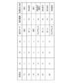
- Fig. 6 is a diagram for explaining the operation of the vehicle lamp 1 of this embodiment.
- Fig. 7A to Fig. 7D are explanatory diagrams of the current flowing through the light source 20. Note that the vertical axis of Fig. 7A to Fig. 7D indicates the value of the current flowing through the light source 20, and the horizontal axis indicates time.
- the output voltage Vdd of the power supply output circuit 11 in FIG. 4 becomes a voltage corresponding to the turn voltage Vt.
- the signal S1 output from the dimming circuit 13A in FIG. 5 becomes H level (duty ratio is 100%).
- the current supply circuit 13B in FIG. 3 supplies a drive current I1 to the light source 20 based on the output voltage Vdd of the power supply output circuit 11 and the signal S1, and lights it up as a turn signal lamp (state No. (2) in FIGS. 6 and 7A). This drive current I1 corresponds to the "first current.”
- the CLL voltage Vc is also at the L level, so the output voltage Vdd of the power supply output circuit 11 in FIG. 4 becomes L level.
- the signal S1 output from the dimming circuit 13A in FIG. 5 also becomes L level (duty ratio is zero%).
- the current supply circuit 13B in FIG. 3 stops supplying drive current to the light source 20 based on the output voltage Vdd (L level) of the power supply output circuit 11 and the signal S1. This causes the light source 20 to turn off (state No. (1) in FIGS. 6 and 7A).
- the light source 20 intermittently lights up (blinks) as a turn signal lamp, as shown in FIG. 7A. Also, when the light source 20 is turned on (when the turn voltage Vt is at H level), the open circuit detection device 100 in FIG. 3 monitors whether the input current flowing through the terminal T1 is greater than a predetermined threshold (performs open circuit detection).
- the output voltage Vdd of the power supply output circuit 11 in FIG. 4 becomes a voltage that corresponds to the CLL voltage Vc.
- the signal S1 output from the dimming circuit 13A in FIG. 5 becomes a signal with a predetermined duty ratio (for example, 15%).
- the current supply circuit 13B in FIG. 3 supplies the light source 20 with a drive current I2 ( ⁇ drive current I1) according to the duty ratio based on the output voltage Vdd of the power output circuit 11 and the signal S1, and turns on the light source 20 with a dim light as a clearance lamp (state No. (4) in FIG. 6 and FIG. 7D).
- This drive current I2 corresponds to the "second current".
- the turn voltage Vt is at L level, the break detection device 100 does not detect a break.
- the output voltage Vdd of the power supply output circuit 11 in FIG. 4 becomes a voltage corresponding to the turn voltage Vt, regardless of the CLL voltage Vc.
- the signal S1 output from the dimming circuit 13A in FIG. 5 becomes the H level (duty ratio is 100%).
- the current supply circuit 13B in FIG. 3 supplies the drive current I1 to the light source 20 based on the output voltage Vdd of the power supply output circuit 11 and the signal S1, and lights it up as a turn signal lamp (state No. (5) in FIG. 6 and FIG. 7C).
- the CLL voltage Vc When the turn voltage Vt is at the L level, the CLL voltage Vc is at the H level, so the output voltage Vdd of the power output circuit 11 in FIG. 4 becomes a voltage according to the CLL voltage Vc.
- the signal S1 output from the dimming circuit 13A in FIG. 5 also becomes at the L level (duty ratio is zero%).
- the current supply circuit 13B in FIG. 3 stops supplying the drive current to the light source 20 based on the signal S1 at the L level (duty ratio is zero%). This causes the light source 20 to turn off (state No. (3) in FIGS. 6 and 7C).
- the light source 20 intermittently lights up (blinks) as a turn signal lamp, as shown in FIG. 7C. Also, when the light source 20 is turned on (when the turn voltage Vt is at H level), the disconnection detection device 100 in FIG. 3 monitors whether the input current flowing through the terminal T1 is greater than a predetermined threshold (performs disconnection detection).
- the output voltage Vdd of the power supply output circuit 11 in FIG. 4 becomes a voltage corresponding to the turn voltage Vt, regardless of the CLL voltage Vc.
- the signal S1 output from the dimming circuit 13A in FIG. 5 becomes the H level (duty ratio is 100%).
- the current supply circuit 13B in FIG. 3 supplies the drive current I1 to the light source 20 based on the output voltage Vdd of the power supply output circuit 11 and the signal S1, and turns on the light source 20 as a turn signal lamp (state No. (6) in FIG. 6 and FIG. 7D). Also, at this time, the disconnection detection device 100 monitors whether the input current flowing through the terminal T1 is greater than a predetermined threshold value (performs disconnection detection).
- the light source 20 were to be turned on based on the CLL voltage Vc, the input current would not flow to the terminal T1 even though the turn voltage Vt is at the H level, which could cause the disconnection detection device 100 to make an erroneous detection.
- the turn voltage Vt and the CLL voltage Vc are both at the H level, the light source 20 is turned on based on the turn voltage Vt (priority is given to the turn voltage Vt), which can prevent erroneous detection.
- the output voltage Vdd of the power supply output circuit 11 in FIG. 4 becomes a voltage corresponding to the CLL voltage Vc.
- the signal S1 output from the dimming circuit 13A in FIG. 5 becomes a signal having a predetermined duty ratio (for example, 15%).
- the current supply circuit 13B in FIG. 3 supplies the light source 20 with a drive current I2 ( ⁇ drive current I1) corresponding to the duty ratio based on the output voltage Vdd of the power supply output circuit 11 and the signal S1, and turns on the light source 20 with a dimmed light as a clearance lamp (state No. (4) in FIG. 6 and FIG. 7D). Note that because the turn voltage Vt is at the L level, the break detection device 100 does not detect a break.
- the light source 20 lights up as a turn signal lamp when the turn voltage Vt is at the H level, and lights up (dimmed) as a clearance lamp when the turn voltage Vt is at the L level.
- the lighting module 10 is a lighting circuit that lights the light source 20 of the vehicle lamp 1, and includes a terminal T1 to which a turn voltage Vt is applied, a terminal T2 to which a CLL voltage Vc is applied, a power output circuit 11, and a drive circuit 13.
- the power output circuit 11 When the turn voltage Vt is applied to the terminal T1, the power output circuit 11 outputs a voltage corresponding to the turn voltage Vt regardless of whether the CLL voltage Vc is applied to the terminal T2, and when the turn voltage Vt is not applied to the terminal T1 and the CLL voltage Vc is applied to the terminal T2, the drive circuit 13 outputs a voltage corresponding to the CLL voltage Vc.
- the drive circuit 13 When a voltage corresponding to the turn voltage Vt is output from the power output circuit 11, the drive circuit 13 supplies a drive current I1 to the light source 20 based on the voltage, and when a voltage corresponding to the CLL voltage Vc is output from the power output circuit 11, the drive circuit 13 supplies a drive current I2 to the light source 20 based on the voltage. In addition, when the turn voltage Vt is applied to the terminal T1, an input current used for disconnection detection of the light source 20 flows. This allows the lighting module 10 (lighting circuit) and the light source 20 to realize two functions (a turn signal lamp function and a clearance lamp function), thereby reducing costs.
- the disconnection detection device 100 detects a disconnection based on the current flowing from the vehicle side (outside the vehicle lamp 1) to the power supply line L1 (in other words, terminal T1). This allows the disconnection detection to be performed appropriately and prevents erroneous detection.
- the lighting module 10 is applied to a vehicle lamp 1, and the turn voltage Vt is a voltage that turns on (blinks) the light source 20 as a turn signal lamp, and the CLL voltage Vc is a voltage that turns on the light source 20 as a clearance lamp. This allows the light source 20 to be turned on as both a turn signal lamp and a clearance lamp.
- the power output circuit 11 also includes a diode D1 with its anode connected to terminal T1, a diode D2 with its anode connected to terminal T2, a PMOS transistor Q1 connected between the cathode of diode D2 and the cathode of diode D1, and a switch control circuit 111.
- the switch control circuit 111 turns off the PMOS transistor Q1 so that a voltage corresponding to the turn voltage Vt is output.
- the switch control circuit 111 turns on the PMOS transistor Q1 so that a voltage corresponding to the CLL voltage Vc is output. This makes it possible to switch the output voltage while preventing reverse current flow to the vehicle side.
- the driving circuit 13 also has a dimming circuit 13A that outputs a signal S1 with a duty ratio based on the state of the light source 20, and a current supply circuit 13B that generates a current that increases as the duty ratio of the signal S1 increases and supplies it to the light source 20.
- the dimming circuit 13A outputs a signal S1 with a duty ratio of 100% (H level) in states No. (2), (5), and (6) in which the light source 20 is turned on based on the turn voltage Vt, outputs a signal S1 with a duty ratio of zero (L level) in states No.
- the vehicle lamp 1 of this embodiment can achieve two functions (turn signal lamp and clearance lamp functions) by using the lighting module 10 and the light source 20.
- the vehicle lamp 1 in the above embodiment is a common turn signal lamp and clearance lamp, but this is not limited to this.
- it can also be used as a tail lamp and brake lamp (stop lamp), etc.
- the light source 20 has multiple light-emitting elements (LEDs) connected in series, but this is not limited to this.
- LEDs light-emitting elements
- multiple light-emitting elements may be connected in parallel.
- the number of light-emitting elements may be one.
Landscapes
- Engineering & Computer Science (AREA)
- Mechanical Engineering (AREA)
- Circuit Arrangement For Electric Light Sources In General (AREA)
Abstract
Description
この出願は、2023年4月24日に出願された日本特許出願、特願2023-071084に基づく優先権を主張し、その内容を援用する。
本実施形態の車両用灯具について説明する前に、一般的な車両用灯具の構成について説明する。
図1は、一般的な車両用灯具1Aの構成を示すブロック図である。
車両用灯具1Aは、光源20A、光源20B、及び点灯モジュール30を備えている。
図1に示すように、光源20A(ターンシグナルランプ)が組み込まれる車両には、車両側(具体的にはバッテリー)から端子Taに流れる電流(入力電流)をモニタできるように断線検知装置100が設けられる。断線検知装置100は、光源20Aが駆動されている際の入力電流を監視し、入力電流の電流値が所定の閾値より小さい場合、光源20Aの複数の発光素子(LED)の何れかに断線があることを検知する。
図2は、車両用灯具1Aの動作を説明するための図である。図1及び図2を参照しつつ、車両用灯具1Aの動作について説明する。
光源20Aは、例えば、ハザードなど、エンジンOFFの状態でも点滅するように設けられている。エンジンOFF(クリアランスもOFF)において、光源20Aを点滅(ON、OFF)させる場合、図2の状態No(1)と状態No(2)で光源20Aの点灯と消灯が交互に繰り返される。具体的には、エンジンOFFにより、CLL電圧Vcは「Lレベル」である。また、クリアランスOFFにより、クリアランス点灯指示信号Scは「Lレベル」である。これにより、クリアランス用点灯回路32は、光源20Bを消灯させる。また、ターン用点灯回路31は、ターン電圧VtがHレベルの期間に、当該ターン電圧Vtに基づいて光源20Aを点灯させ(状態No(2))、ターン電圧VtがLレベルの期間には、光源20Aを消灯させる(状態No(1))。
クリアランスランプ用の光源20Bを点灯させる場合には、エンジンがONの状態となっており、端子Tbに印加されるCLL電圧Vcは「Hレベル」である。また、前述したように光源20Bを点灯させる際に、クリアランス点灯指示信号Scは「Hレベル」となる。クリアランス点灯指示信号Scが「Hレベル」であることにより、調光回路33は、所定のデューティ比(例えば15%)の信号を出力する。また、ターンOFFにより、端子Taに印加される電圧(ターン電圧Vt)は「Lレベル」である。
エンジンON(CLL電圧Vcが「Hレベル」)の状態において、光源20Aのみを点灯(点滅)させる場合、クリアランス点灯指示信号Scは「Lレベル」である。クリアランス点灯指示信号Scが「Lレベル」であることにより、クリアランス用点灯回路32は、光源20Bを消灯させる。また、ターン用点灯回路31は、ターン電圧VtがHレベルの期間に、当該ターン電圧Vtに基づいて光源20Aを点灯させ(状態No(5))、ターン電圧VtがLレベルの期間には、光源20Aを消灯させる(状態No(3))。
エンジンON(CLL電圧Vcが「Hレベル」)の状態において、光源20Aと光源20Bの両方を点灯させる場合、クリアランス点灯指示信号Scは「Hレベル」となり、調光回路33は、所定のデューティ比(例えば15%)の信号を出力する。
図3は、本実施形態の車両用灯具1の構成を示すブロック図である。
本実施形態の車両用灯具1は、点灯モジュール10と光源20を備えている。
点灯モジュール10は、図3に示すように電源出力回路11、駆動回路13、制御IC15、及び端子T1~T5を備えている。なお、端子T1~T3は、図1の端子Ta~Tcにそれぞれ対応している。つまり、端子T1は電源ラインL1に接続されており、パルス状のターン電圧Vtが印加される。また、端子T2は電源ラインL2に接続されており、CLL電圧Vcが印加される。また、端子T3にはクリアランス点灯指示信号Scが印加される。本実施形態において、ターン電圧Vtは「第1電源電圧」に相当し、端子T1は「第1端子」に相当する。また、CLL電圧Vcは「第2電源電圧」に相当し、端子T2は「第2端子」に相当する。
図4は、電源出力回路11の構成の一例を示す図である。
図4に示す電源出力回路11は、ダイオードD1,D2、PMOSトランジスタQ1、及びスイッチ制御回路111を備えている。
ターン電圧VtがHレベルのとき、スイッチ制御回路111のNPNトランジスタQ2がオンする。また、NPNトランジスタQ2がオンすることにより、PNPトランジスタQ3がオンする。これにより、PMOSトランジスタQ1のゲート・ソース間が同電位となるためPMOSトランジスタQ1はオフする。つまり、CLL電圧Vcの値(Hレベル,Lレベル)に関わらず、PMOSトランジスタQ1はオフとなる。換言すると、ターン電圧Vtが端子T1に印加された場合には、スイッチ制御回路111は、電源出力回路11からターン電圧Vtに応じた電圧(具体的には、ダイオードD1の順方向電圧(例えば0.7V)低下した電圧)が出力されるようPMOSトランジスタQ1をオフに制御する。この際、ダイオードD2は、PMOSトランジスタQ1の寄生ダイオードを介して、端子T2へ電流が流れること(車両側への逆流)を防止する。なお、このときの電源出力回路11の出力電圧Vdd(ターン電圧Vtに応じた電圧)は「第1電圧」に相当する。
ターン電圧VtがLレベルのとき、スイッチ制御回路111のNPNトランジスタQ2がオフする。またNPNトランジスタQ2がオフすることにより、PNPトランジスタQ3もオフする。よって、CLL電圧Vcに応じた電圧(具体的には、ダイオードD2の順方向電圧(例えば0.7V)低下した電圧)が、抵抗R3と抵抗R4で分圧され、その分圧電圧がPMOSトランジスタQ1のゲートに印加される。これにより、PMOSトランジスタQ1のゲート・ソース間電圧が閾値を超えてPMOSトランジスタQ1がオンする。よって、電源出力回路11からはCLL電圧Vcに応じた電圧(ダイオードD2およびPMOSトランジスタQ1を介した電圧)が出力される。換言すると、スイッチ制御回路111は、ターン電圧Vtが端子T1に印加されずに、CLL電圧Vcが端子T2に印加された場合、電源出力回路11からCLL電圧Vcに応じた電圧が出力されるようPMOSトランジスタQ1をオンに制御する。この際、ダイオードD1は、端子T1へ電流が流れること(車両側への逆流)を防止する。なお、このときの電源出力回路11の出力電圧Vdd(CLL電圧Vcに応じた電圧)は「第2電圧」に相当する。
図5は、調光回路13Aの構成の一例を示す図である。調光回路13Aは、発振回路131、抵抗R10~R14、NPNトランジスタQ4,Q5,Q7、PNPトランジスタQ6を備えている。
この場合、上述したようにオペアンプOP1の出力がHレベル(電源電圧Vcc)となるため、抵抗R6は、抵抗R7と並列に接続された状態となる。すなわち、オペアンプOP1の+端子の電圧は、抵抗R7と抵抗R8のみによる電源電圧Vccの分圧電圧よりも高くなる。ここでは、抵抗R6,R7,R8の抵抗値が全て同じであるため、オペアンプOP1の+端子の電圧は、2/3Vcc(Vccが7Vの場合、約4.6V)となる。
この場合、上述したようにオペアンプOP1の出力がLレベル(接地電圧)となるため、抵抗R6は、抵抗R8と並列に接続された状態となる。すなわち、オペアンプOP1の+端子の電圧は、抵抗R7と抵抗R8のみによる電源電圧Vccの分圧電圧よりも低くなる。ここでは、抵抗R6,R7,R8の抵抗値が全て同じであるため、オペアンプOP1の+端子の電圧は、1/3Vcc(Vccが7Vの場合、約2.3V)となる。
次に、調光回路13Aの動作について説明する。
ターン電圧VtがHレベルのとき、NPNトランジスタQ7がオンする。NPNトランジスタQ7がオンすることにより、発振回路131のコンデンサC2に蓄えられた電荷が放出(コンデンサC2が放電)される。
ターン電圧VtがLレベルのとき、NPNトランジスタQ7はオフする。また、クリアランス点灯指示信号ScがHレベルであることにより、NPNトランジスタQ4がオンし、NPNトランジスタQ5はベースに電流が供給されないためオフする。これにより、PNPトランジスタQ6もオフする。
ターン電圧VtがLレベルのとき、上述したようにNPNトランジスタQ7はオフする。また、クリアランス点灯指示信号ScがLレベルであることにより、NPNトランジスタQ4がオフし、NPNトランジスタQ5のベースには、電源電圧Vccから抵抗R10を介して電流が供給されるのでNPNトランジスタQ5がオンする。NPNトランジスタQ5がオンすることにより、PNPトランジスタQ6がオンし、電源電圧Vccから、抵抗R12、PNPトランジスタQ6を介して発振回路131のコンデンサC2に電流が流れ、コンデンサC2が充電される。
図6は、本実施形態の車両用灯具1の動作を説明するための図である。また、図7A~図7Dは、光源20に流れる電流の説明図である。なお、図7A~図7Dの縦軸は光源20に流れる電流値を示しており、横軸は時間を示している。
前述したように、この場合、CLL電圧Vcが「Lレベル」、クリアランス点灯指示信号Scが「Lレベル」であり、ターン電圧Vtは所定周期で「Hレベル」と「Lレベル」を交互に繰り返す。
前述したように、この場合、CLL電圧Vcは「Hレベル」であり、クリアランス点灯指示信号Scも「Hレベル」である。また、ターンOFFにより、端子Taに印加される電圧(ターン電圧Vt)は「Lレベル」である。
前述したように、この場合、CLL電圧Vcは「Hレベル」、クリアランス点灯指示信号Scは「Lレベル」である。また、ターン電圧Vtは所定周期で「Hレベル」と「Lレベル」を交互に繰り返す。
前述したように、この場合、CLL電圧Vcは「Hレベル」、クリアランス点灯指示信号Scは「Hレベル」である。また、ターン電圧Vtは所定周期で「Hレベル」と「Lレベル」を交互に繰り返す。
以上、本実施形態の点灯モジュール10について説明した。点灯モジュール10は、車両用灯具1の光源20を点灯させる点灯回路であって、ターン電圧Vtが印加される端子T1と、CLL電圧Vcが印加される端子T2と、電源出力回路11と、駆動回路13とを備えている。電源出力回路11は、ターン電圧Vtが端子T1に印加された場合、CLL電圧Vcが端子T2に印加されるか否かにかかわらず、ターン電圧Vtに応じた電圧を出力し、ターン電圧Vtが端子T1に印加されずに、CLL電圧Vcが端子T2に印加されるとCLL電圧Vcに応じた電圧を出力する。駆動回路13は、電源出力回路11からターン電圧Vtに応じた電圧が出力される場合、その電圧に基づいて光源20に駆動電流I1を供給し、電源出力回路11からCLL電圧Vcに応じた電圧出力される場合、その電圧に基づいて光源20に駆動電流I2を供給する。また、端子T1には、ターン電圧Vtが印加される際に、光源20の断線検知に用いられる入力電流が流れる。これにより、点灯モジュール10(点灯回路)と光源20で、2つの機能(ターンシグナルランプの機能,クリアランスランプの機能)を実現できる。よって、コストの低減を図ることができる。
上記の実施形態は、本発明の理解を容易にするためのものであり、本発明を限定して解釈するためのものではない。また、本発明は、その趣旨を逸脱することなく、変更や改良され得るとともに、本発明にはその等価物が含まれるのはいうまでもない。
10 点灯モジュール
11 電源出力回路
13 駆動回路
13A 調光回路
13B 電流供給回路
15 制御IC
20,20A,20B 光源
30 点灯モジュール
31 ターン用点灯回路
32 クリアランス用点灯回路
33 調光回路
100 断線検知装置
111 スイッチ制御回路
131 発振回路
151 電源回路
C1,C2 コンデンサ
T1~T5,Ta~Tg 端子
L1,L2 電源ライン
OP1 オペアンプ
Q1 PMOSトランジスタ
Q2,Q4,Q5,Q7 NPNトランジスタ
Q3,Q6 PNPトランジスタ
R1~R14 抵抗
Vt ターン用電源電圧(ターン電圧)
Vc クリアランス用電源電圧(CLL電圧)
Vcc 電源電圧
Sc クリアランス点灯指示信号
Claims (6)
- 光源を点灯させる点灯回路であって、
第1電源電圧が印加される第1端子と、
第2電源電圧が印加される第2端子と、
前記第1電源電圧が前記第1端子に印加された場合、前記第2電源電圧が前記第2端子に印加されるか否かにかかわらず、前記第1電源電圧に応じた第1電圧を出力し、前記第1電源電圧が前記第1端子に印加されずに、前記第2電源電圧が前記第2端子に印加された場合、前記第2電源電圧に応じた第2電圧を出力する電源出力回路と、
前記電源出力回路から前記第1電圧が出力される場合、前記第1電圧に基づいて前記光源に第1電流を供給し、前記電源出力回路から前記第2電圧が出力される場合、前記第2電圧に基づいて前記光源に第2電流を供給する駆動回路と、
を備え、
前記第1端子には、前記第1電源電圧が印加される際に、前記光源の断線検知に用いられる入力電流が流れる、
点灯回路。 - 請求項1に記載の点灯回路であって、
前記第1電流の電流値は、前記第2電流の電流値よりも大きい、
点灯回路。 - 請求項1に記載の点灯回路であって、
前記電源出力回路は、
前記第1端子にアノードが接続された第1ダイオードと、
前記第2端子にアノードが接続された第2ダイオードと、
前記第2ダイオードのカソードと、前記第1ダイオードのカソードとの間に接続されたスイッチと、
前記第1電源電圧が前記第1端子に印加された場合には、前記第1電圧が出力されるよう前記スイッチをオフし、前記第1電源電圧が前記第1端子に印加されずに、前記第2電源電圧が前記第2端子に印加された場合、前記第2電圧が出力されるよう前記スイッチをオンするスイッチ制御回路と、
を含む点灯回路。 - 請求項1に記載の点灯回路であって、
前記駆動回路は、
前記光源の状態に基づいたデューティ比の信号を出力する調光回路と、
前記デューティ比の上昇に応じて大きくなる電流を生成し、前記光源に供給する電流供給回路と、
を有し、
前記調光回路は、
前記第1電源電圧に基づいて前記光源を点灯させる第1状態には、第1デューティ比を有する前記信号を出力し、
前記光源を消灯させる第2状態には、前記デューティ比がゼロとなる前記信号を出力し、
前記第2電源電圧に基づいて前記光源を点灯させる第3状態には、前記第1デューティ比よりも小さい第2デューティ比を有する前記信号を出力する、
点灯回路。 - 車両用灯具に適用される請求項1に記載の点灯回路であって、
前記第1電源電圧は、前記光源をターンシグナルランプとして点灯させる電圧であり、
前記第2電源電圧は、前記光源をクリアランスランプとして点灯させる電圧である、
点灯回路。 - 請求項1~5の何れか一項に記載の点灯回路と、
前記光源と、
を備える車両用灯具。
Priority Applications (1)
| Application Number | Priority Date | Filing Date | Title |
|---|---|---|---|
| JP2025516612A JPWO2024224902A1 (ja) | 2023-04-24 | 2024-03-25 |
Applications Claiming Priority (2)
| Application Number | Priority Date | Filing Date | Title |
|---|---|---|---|
| JP2023-071084 | 2023-04-24 | ||
| JP2023071084 | 2023-04-24 |
Publications (1)
| Publication Number | Publication Date |
|---|---|
| WO2024224902A1 true WO2024224902A1 (ja) | 2024-10-31 |
Family
ID=93256145
Family Applications (1)
| Application Number | Title | Priority Date | Filing Date |
|---|---|---|---|
| PCT/JP2024/011621 Ceased WO2024224902A1 (ja) | 2023-04-24 | 2024-03-25 | 点灯回路、および車両用灯具 |
Country Status (2)
| Country | Link |
|---|---|
| JP (1) | JPWO2024224902A1 (ja) |
| WO (1) | WO2024224902A1 (ja) |
Citations (2)
| Publication number | Priority date | Publication date | Assignee | Title |
|---|---|---|---|---|
| JP2006062591A (ja) * | 2004-08-30 | 2006-03-09 | Yazaki Corp | 車室外ランプ制御システム |
| WO2013001574A1 (ja) * | 2011-06-29 | 2013-01-03 | 三菱電機株式会社 | Led点灯装置 |
-
2024
- 2024-03-25 WO PCT/JP2024/011621 patent/WO2024224902A1/ja not_active Ceased
- 2024-03-25 JP JP2025516612A patent/JPWO2024224902A1/ja active Pending
Patent Citations (2)
| Publication number | Priority date | Publication date | Assignee | Title |
|---|---|---|---|---|
| JP2006062591A (ja) * | 2004-08-30 | 2006-03-09 | Yazaki Corp | 車室外ランプ制御システム |
| WO2013001574A1 (ja) * | 2011-06-29 | 2013-01-03 | 三菱電機株式会社 | Led点灯装置 |
Also Published As
| Publication number | Publication date |
|---|---|
| JPWO2024224902A1 (ja) | 2024-10-31 |
Similar Documents
| Publication | Publication Date | Title |
|---|---|---|
| US10420196B2 (en) | Lighting circuit and vehicle lamp having the same | |
| JP3633522B2 (ja) | 負荷駆動回路 | |
| JP2006103404A (ja) | 車両用灯具の点灯制御回路 | |
| US9162607B2 (en) | Vehicular lamp | |
| CN108924989B (zh) | 点灯电路及使用该点灯电路的车辆用灯具 | |
| JP2016122643A (ja) | 点灯回路およびそれを用いた車両用灯具 | |
| JP6302706B2 (ja) | 車両用灯具およびその駆動装置 | |
| JP6173874B2 (ja) | 車両用灯具 | |
| US10368405B2 (en) | Two stage indicator dimming circuit controlled by PWM backlighting back feed and backlight control | |
| CN114982379B (zh) | 点亮电路以及车辆用方向指示灯 | |
| WO2024224902A1 (ja) | 点灯回路、および車両用灯具 | |
| US10728985B2 (en) | Vehicle lamp and lighting circuit | |
| JP7796728B2 (ja) | 車両用灯具 | |
| JP2022118963A (ja) | 点灯回路 | |
| CN111405702B (zh) | 灯光系统 | |
| US12167518B2 (en) | Light source module and lighting circuit | |
| WO2023106199A1 (ja) | 点灯回路、及び車両用灯具 | |
| US20120092151A1 (en) | Electronic Control Circuit for Lamps of a Vehicle | |
| JP2011073509A (ja) | 車載ランプ点灯制御回路 | |
| JP7675637B2 (ja) | 点灯回路、及び車両用灯具 | |
| JP4468983B2 (ja) | 負荷制御装置 | |
| JP2025084555A (ja) | 点灯回路 | |
| JP2025035188A (ja) | 点灯回路 | |
| JP6249555B2 (ja) | 車両用灯具 | |
| WO2024080187A1 (ja) | 点灯回路 |
Legal Events
| Date | Code | Title | Description |
|---|---|---|---|
| 121 | Ep: the epo has been informed by wipo that ep was designated in this application |
Ref document number: 24796660 Country of ref document: EP Kind code of ref document: A1 |
|
| ENP | Entry into the national phase |
Ref document number: 2025516612 Country of ref document: JP Kind code of ref document: A |
|
| WWE | Wipo information: entry into national phase |
Ref document number: 2025516612 Country of ref document: JP |
|
| NENP | Non-entry into the national phase |
Ref country code: DE |
|
| 122 | Ep: pct application non-entry in european phase |
Ref document number: 24796660 Country of ref document: EP Kind code of ref document: A1 |