WO2024219268A1 - 基板 - Google Patents
基板 Download PDFInfo
- Publication number
- WO2024219268A1 WO2024219268A1 PCT/JP2024/014235 JP2024014235W WO2024219268A1 WO 2024219268 A1 WO2024219268 A1 WO 2024219268A1 JP 2024014235 W JP2024014235 W JP 2024014235W WO 2024219268 A1 WO2024219268 A1 WO 2024219268A1
- Authority
- WO
- WIPO (PCT)
- Prior art keywords
- layer
- electrode
- substrate
- sample
- substrate according
- Prior art date
- Legal status (The legal status is an assumption and is not a legal conclusion. Google has not performed a legal analysis and makes no representation as to the accuracy of the status listed.)
- Ceased
Links
Images




Classifications
-
- C—CHEMISTRY; METALLURGY
- C23—COATING METALLIC MATERIAL; COATING MATERIAL WITH METALLIC MATERIAL; CHEMICAL SURFACE TREATMENT; DIFFUSION TREATMENT OF METALLIC MATERIAL; COATING BY VACUUM EVAPORATION, BY SPUTTERING, BY ION IMPLANTATION OR BY CHEMICAL VAPOUR DEPOSITION, IN GENERAL; INHIBITING CORROSION OF METALLIC MATERIAL OR INCRUSTATION IN GENERAL
- C23C—COATING METALLIC MATERIAL; COATING MATERIAL WITH METALLIC MATERIAL; SURFACE TREATMENT OF METALLIC MATERIAL BY DIFFUSION INTO THE SURFACE, BY CHEMICAL CONVERSION OR SUBSTITUTION; COATING BY VACUUM EVAPORATION, BY SPUTTERING, BY ION IMPLANTATION OR BY CHEMICAL VAPOUR DEPOSITION, IN GENERAL
- C23C28/00—Coating for obtaining at least two superposed coatings either by methods not provided for in a single one of groups C23C2/00 - C23C26/00 or by combinations of methods provided for in subclasses C23C and C25C or C25D
-
- C—CHEMISTRY; METALLURGY
- C23—COATING METALLIC MATERIAL; COATING MATERIAL WITH METALLIC MATERIAL; CHEMICAL SURFACE TREATMENT; DIFFUSION TREATMENT OF METALLIC MATERIAL; COATING BY VACUUM EVAPORATION, BY SPUTTERING, BY ION IMPLANTATION OR BY CHEMICAL VAPOUR DEPOSITION, IN GENERAL; INHIBITING CORROSION OF METALLIC MATERIAL OR INCRUSTATION IN GENERAL
- C23C—COATING METALLIC MATERIAL; COATING MATERIAL WITH METALLIC MATERIAL; SURFACE TREATMENT OF METALLIC MATERIAL BY DIFFUSION INTO THE SURFACE, BY CHEMICAL CONVERSION OR SUBSTITUTION; COATING BY VACUUM EVAPORATION, BY SPUTTERING, BY ION IMPLANTATION OR BY CHEMICAL VAPOUR DEPOSITION, IN GENERAL
- C23C28/00—Coating for obtaining at least two superposed coatings either by methods not provided for in a single one of groups C23C2/00 - C23C26/00 or by combinations of methods provided for in subclasses C23C and C25C or C25D
- C23C28/02—Coating for obtaining at least two superposed coatings either by methods not provided for in a single one of groups C23C2/00 - C23C26/00 or by combinations of methods provided for in subclasses C23C and C25C or C25D only coatings only including layers of metallic material
-
- C—CHEMISTRY; METALLURGY
- C25—ELECTROLYTIC OR ELECTROPHORETIC PROCESSES; APPARATUS THEREFOR
- C25B—ELECTROLYTIC OR ELECTROPHORETIC PROCESSES FOR THE PRODUCTION OF COMPOUNDS OR NON-METALS; APPARATUS THEREFOR
- C25B11/00—Electrodes; Manufacture thereof not otherwise provided for
- C25B11/04—Electrodes; Manufacture thereof not otherwise provided for characterised by the material
- C25B11/051—Electrodes formed of electrocatalysts on a substrate or carrier
- C25B11/052—Electrodes comprising one or more electrocatalytic coatings on a substrate
- C25B11/053—Electrodes comprising one or more electrocatalytic coatings on a substrate characterised by multilayer electrocatalytic coatings
-
- C—CHEMISTRY; METALLURGY
- C25—ELECTROLYTIC OR ELECTROPHORETIC PROCESSES; APPARATUS THEREFOR
- C25B—ELECTROLYTIC OR ELECTROPHORETIC PROCESSES FOR THE PRODUCTION OF COMPOUNDS OR NON-METALS; APPARATUS THEREFOR
- C25B11/00—Electrodes; Manufacture thereof not otherwise provided for
- C25B11/04—Electrodes; Manufacture thereof not otherwise provided for characterised by the material
- C25B11/051—Electrodes formed of electrocatalysts on a substrate or carrier
- C25B11/055—Electrodes formed of electrocatalysts on a substrate or carrier characterised by the substrate or carrier material
- C25B11/057—Electrodes formed of electrocatalysts on a substrate or carrier characterised by the substrate or carrier material consisting of a single element or compound
- C25B11/067—Inorganic compound e.g. ITO, silica or titania
-
- C—CHEMISTRY; METALLURGY
- C25—ELECTROLYTIC OR ELECTROPHORETIC PROCESSES; APPARATUS THEREFOR
- C25B—ELECTROLYTIC OR ELECTROPHORETIC PROCESSES FOR THE PRODUCTION OF COMPOUNDS OR NON-METALS; APPARATUS THEREFOR
- C25B11/00—Electrodes; Manufacture thereof not otherwise provided for
- C25B11/04—Electrodes; Manufacture thereof not otherwise provided for characterised by the material
- C25B11/051—Electrodes formed of electrocatalysts on a substrate or carrier
- C25B11/073—Electrodes formed of electrocatalysts on a substrate or carrier characterised by the electrocatalyst material
- C25B11/075—Electrodes formed of electrocatalysts on a substrate or carrier characterised by the electrocatalyst material consisting of a single catalytic element or catalytic compound
- C25B11/081—Electrodes formed of electrocatalysts on a substrate or carrier characterised by the electrocatalyst material consisting of a single catalytic element or catalytic compound the element being a noble metal
-
- C—CHEMISTRY; METALLURGY
- C25—ELECTROLYTIC OR ELECTROPHORETIC PROCESSES; APPARATUS THEREFOR
- C25B—ELECTROLYTIC OR ELECTROPHORETIC PROCESSES FOR THE PRODUCTION OF COMPOUNDS OR NON-METALS; APPARATUS THEREFOR
- C25B11/00—Electrodes; Manufacture thereof not otherwise provided for
- C25B11/04—Electrodes; Manufacture thereof not otherwise provided for characterised by the material
- C25B11/051—Electrodes formed of electrocatalysts on a substrate or carrier
- C25B11/073—Electrodes formed of electrocatalysts on a substrate or carrier characterised by the electrocatalyst material
- C25B11/075—Electrodes formed of electrocatalysts on a substrate or carrier characterised by the electrocatalyst material consisting of a single catalytic element or catalytic compound
- C25B11/089—Alloys
-
- C—CHEMISTRY; METALLURGY
- C25—ELECTROLYTIC OR ELECTROPHORETIC PROCESSES; APPARATUS THEREFOR
- C25B—ELECTROLYTIC OR ELECTROPHORETIC PROCESSES FOR THE PRODUCTION OF COMPOUNDS OR NON-METALS; APPARATUS THEREFOR
- C25B11/00—Electrodes; Manufacture thereof not otherwise provided for
- C25B11/04—Electrodes; Manufacture thereof not otherwise provided for characterised by the material
- C25B11/051—Electrodes formed of electrocatalysts on a substrate or carrier
- C25B11/073—Electrodes formed of electrocatalysts on a substrate or carrier characterised by the electrocatalyst material
- C25B11/091—Electrodes formed of electrocatalysts on a substrate or carrier characterised by the electrocatalyst material consisting of at least one catalytic element and at least one catalytic compound; consisting of two or more catalytic elements or catalytic compounds
- C25B11/097—Electrodes formed of electrocatalysts on a substrate or carrier characterised by the electrocatalyst material consisting of at least one catalytic element and at least one catalytic compound; consisting of two or more catalytic elements or catalytic compounds comprising two or more noble metals or noble metal alloys
-
- H—ELECTRICITY
- H05—ELECTRIC TECHNIQUES NOT OTHERWISE PROVIDED FOR
- H05K—PRINTED CIRCUITS; CASINGS OR CONSTRUCTIONAL DETAILS OF ELECTRIC APPARATUS; MANUFACTURE OF ASSEMBLAGES OF ELECTRICAL COMPONENTS
- H05K1/00—Printed circuits
- H05K1/02—Details
- H05K1/09—Use of materials for the conductive, e.g. metallic pattern
Definitions
- the present disclosure relates to a substrate that is used under conditions in which at least a portion of the electrode is in contact with a solution containing an electrolyte.
- Patent Document 1 discloses a wiring board having a plurality of first pads with copper exposed on the surface and a plurality of second pads with a gold plating layer deposited on the surface.
- the substrate according to one embodiment of the present disclosure comprises a ceramic base having a first surface and an electrode located on the first surface, the electrode including a conductor layer including an Au layer and a Pt layer deposited on the conductor layer, and is used under conditions in which at least a portion of the electrode is in contact with a solution including an electrolyte.
- FIG. 1 is a schematic cross-sectional view of a pump including a substrate according to a first embodiment of the present disclosure.
- FIG. 2 is a partial cross-sectional view of a substrate according to a first embodiment of the present disclosure.
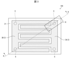
- FIG. 2 is a top view of the substrate according to the first embodiment of the present disclosure.
- FIG. 2 is a bottom view of the substrate according to the first embodiment of the present disclosure.
- FIG. 11 is a top view of a substrate according to a second embodiment of the present disclosure.
- FIG. 1 is a schematic diagram of a test device and a sample used in a voltage application test. 1 is a current-potential curve showing the results of LSV measurement. 13 is a graph showing a change in current when the voltage is changed in increments of 0.5 V.
- FIG. 1 is a graph showing the change in current over time when a constant voltage of 5 V is applied.
- FIG. 4 is a diagram showing measurement points in an electrode portion of a sample.
- 11 is a graph showing the results of measuring the thickness over time at each measurement point shown in FIG. 10 for each layer of the sample.
- 11 is a graph showing the results of measuring the thickness over time at each measurement point shown in FIG. 10 for each layer of the sample.
- the wiring board is to be used in applications such as actuator pumps, it is necessary to consider the possibility of exposing at least a portion of the electrodes to a condition in which they come into contact with a solution containing an electrolyte.
- One aspect of the present disclosure provides a substrate that can be used under conditions in which at least a portion of the electrode is in contact with a solution containing an electrolyte.
- a substrate that can be used under conditions in which at least a portion of the electrode is in contact with a solution containing an electrolyte.
- top and bottom is for convenience and does not limit the top and bottom when the substrate is actually used.
- the first surface 21 on which the electrode 3 is provided in the substrate 100 is defined as the top surface.
- the dimensions of each component and the dimensional ratio between each component may differ from the actual ones.
- the structure of the electrode 3 and the external electrode 5 may be exaggerated in thickness to facilitate the explanation of the laminated structure.
- FIG. 1 is a schematic cross-sectional view of a pump 900 including a substrate 100 according to the present disclosure.
- the substrate 100 according to the present disclosure may be used as a component of a pump 900, for example, as shown in FIG. 1.
- the pump 900 includes a substrate 100 having electrodes 3, and a liquid delivery section 9.
- the liquid delivery section 9 includes a conductive liquid storage section 91 that stores the conductive liquid EL, a liquid storage section 93 that stores the liquid agent ML, which is the liquid to be ejected, and a partition wall 92 located between the conductive liquid storage section 91 and the liquid agent storage section 93.
- a conductive liquid EL for example, a NaCl solution such as saline can be used.
- the partition wall 92 is made of, for example, silicone rubber, and can transmit the oscillation of the conductive liquid EL to the liquid agent ML.
- the pump 900 is an actuator-type pump that applies a voltage via the external electrode 5 of the substrate 100 to oscillate the conductive liquid EL and push up the partition 92, thereby discharging the liquid agent ML.
- the voltage applied to the substrate 100 may be approximately 3 V.
- the electrode 3 of the substrate 100 comes into contact with a conductive liquid EL that contains an electrolyte.
- Fig. 2 is a partial cross-sectional view of the substrate 100 according to embodiment 1.
- Fig. 3 is a top view of the substrate 100.
- Fig. 4 is a bottom view of the substrate 100.
- Fig. 2 shows a cross section of a region R in Fig. 3 .
- the substrate 100 has a ceramic base 2 having a first surface 21 and a second surface 22 located opposite the first surface 21, and an electrode 3 located on the first surface 21.
- the electrode 3 includes an anode 3A and a cathode 3B.
- a bonding layer 4 may be located between the electrode 3 and the ceramic base 2.
- An external electrode 5 is located on the second surface 22. The external electrode 5 is electrically connected to the electrode 3 via a through conductor 6.
- the ceramic base 2 may be an insulator made of an insulating material containing a ceramic material.
- the ceramic base 2 may be an insulator made of a ceramic material containing 70% or more by mass of alumina.
- the ceramic base 2 may be a composite ceramic containing 70% or more by mass of alumina and 5 to 30% by mass of zirconia.
- the substrate 100 is used under conditions in which it comes into contact with a solution containing an electrolyte, and in this case, some materials may have low resistance to the solution.
- the ceramic base 2 out of a ceramic material containing 70% or more by mass of alumina, it is possible to improve the resistance to the solution. Also, by making it a composite ceramic containing zirconia, it is possible to improve the strength and toughness of the ceramic base 2.
- the bonding layer 4 is a layer provided to improve the bonding between the ceramic base 2 and the electrode 3.
- the thickness of the bonding layer 4 may be 0.01 ⁇ m or more and 0.30 ⁇ m or less.
- the bonding layer 4 may be, for example, a Ti layer containing 10 mass % or more of Ti.
- the Ti layer may be a layer made of Ti.
- Ti can effectively function as a main component constituting the bonding layer because it can strengthen the bond between the ceramic base 2 and the metal layer contained in the electrode 3.
- the bonding strength between the ceramic base 2 and the electrode 3 can be improved.
- the function of the bonding layer 4 can be sufficiently ensured.
- the electrode 3 may be a pair of comb-shaped electrodes including an anode 3A and a cathode 3B.
- the structure of the electrode 3 described below is common to the anode 3A and the cathode 3B unless otherwise specified.
- the electrode 3 has a layered structure including a conductor layer 31 and a Pt layer 32 deposited on the conductor layer 31.
- the conductor layer 31 includes an Au layer 311.
- the Au layer 311 may be a layer mainly composed of Au. Specifically, the Au layer 311 may be a layer containing 98% or more by mass of Au, more preferably 99.99% or more by mass. Alternatively, the Au layer 311 may be a layer made of Au. Au is a metal with low resistance. By including an Au layer in the conductor layer 31, a high-quality electrode and substrate with low resistance can be realized.
- the thickness of the entire electrode 3 is generally 1.0 ⁇ m or more and 3.0 ⁇ m or less.
- the thickness of the Au layer may be, for example, 0.05 ⁇ m or more and 2.00 ⁇ m or less.
- the conductor layer 31 By including an Au layer with a thickness of 0.05 ⁇ m or more and 2.00 ⁇ m or less in the conductor layer 31, a high-quality electrode with low resistance can be realized.
- the Au layer may be thicker than the other metal layers.
- the Au layer 311 may have a thickness three or more times that of the other metal layers contained in the conductor layer 31.
- the conductor layer 31 may include a second Pt layer 312 located in contact with the bonding layer 4.
- the conductor layer 31 may include an Au layer 311 and a second Pt layer 312 located between the Au layer 311 and the bonding layer 4.
- the second Pt layer 312 may be a layer containing Pt as a main component.
- the second Pt layer 312 may be a layer containing 98% by mass or more of Pt, more preferably 99.9% by mass or more.
- the second Pt layer 312 may be a layer made of Pt.
- the thickness of the second Pt layer 312 may be, for example, 0.05 ⁇ m or more and 0.50 ⁇ m or less. By making the thickness of the second Pt layer 312 0.05 ⁇ m or more, it is possible to easily form the second Pt layer 312. In addition, by making the thickness of the second Pt layer 312 0.50 ⁇ m or less, it is possible to prevent excessive use of expensive Pt.
- the conductor layer 31 may include a Pd layer instead of the second Pt layer 312.
- the Pd layer may be a layer mainly composed of Pd.
- the Pd layer may be a layer made of Pd.
- the Pd layer is located between the Au layer 311 and the bonding layer 4, thereby further improving the bonding strength between the conductor layer 31 and the bonding layer 4.
- the thickness of the Pd layer may be, for example, 0.05 ⁇ m or more and 0.50 ⁇ m or less. The thickness of the Pd layer being 0.05 ⁇ m or more makes it easier to form the Pd layer. In addition, the thickness of the Pd layer being 0.50 ⁇ m or less makes it possible to suppress excessive use of expensive precious metals such as Pt.
- the Pt layer 32 is a layer located on the outermost surface of the electrode 3.
- the Pt layer 32 may be a layer made of Pt.
- the Pt layer 32 may be a layer containing 98% by mass or more of Pt, more preferably 99.9% by mass or more.
- the Pt layer 32 is deposited on the conductor layer 31 so as to cover the upper surface of the conductor layer 31.
- the Pt layer 32 may cover the entire exposed surface of the conductor layer 31.
- the thickness of the Pt layer may be 0.05 ⁇ m or more and 0.50 ⁇ m or less.
- Electrode 3 When at least a portion of electrode 3 is in contact with a solution containing an electrolyte and a voltage equal to or greater than a certain voltage is applied, the Au contained in electrode 3 may come into contact with the solution, causing Au to dissolve into the solution.
- the inventors have found that Pt dissolves very little or not at all in solution even under the same conditions as Au.
- the solution containing an electrolyte is a NaCl solution
- the mechanism by which Au dissolves into the solution is due to the chemical reaction shown in the following chemical formula (1). Tests related to this finding are described in detail in the section entitled "Demonstration Tests" below.
- the electrode 3 is composed of the conductor layer 31 and the Pt layer 32 covering the conductor layer 31, the contact area between the Au layer included in the conductor layer 31 and the solution is significantly reduced. However, even when the electrode 3 is used under conditions in which at least a part of the electrode 3 is in contact with a solution containing an electrolyte, dissolution of the metal constituting the electrode 3 can be significantly reduced, and the quality of the substrate can be maintained. In this way, a substrate that can be stably used under conditions in which at least a part of the electrode 3 is in contact with a solution containing an electrolyte can be realized. The thickness necessary for protection can be ensured. By making the thickness of the Pt layer 32 0.50 ⁇ m or less, excessive use of expensive Pt can be suppressed.
- the external electrodes 5 are electrodes to which a potential corresponding to the voltage supplied to the substrate 100 is applied.
- the substrate 100 has four external electrodes 5. Two of the four external electrodes 5 are electrically connected to the anode 3A via the through conductors 6, and the remaining two are electrically connected to the cathode 3B via the through conductors 6. In Figures 3 and 4, the positions of the through conductors 6 are indicated by dashed lines.
- the four external electrodes may be located at each corner of the second surface 22 of the rectangular ceramic base 2.
- the external electrode 5 has a conductor layer 31.
- a bonding layer 4 may be located between the external electrode 5 and the ceramic substrate 2.
- the bonding layer 4 and the conductor layer 31 may have the same configuration as the bonding layer 4 and the conductor layer 31 of the electrode 3.
- the external electrode 5 since the external electrode 5 is located on the second surface 22, it is unlikely to come into contact with a solution containing an electrolyte. Therefore, the external electrode 5 may not have a Pt layer 32 covering the conductor layer 31.
- the external electrode 5 may include a conductor layer 31 including an Au layer 311, and the conductor layer 31 may be formed on the outermost surface and exposed.
- the outermost layer of the electrode 3 may be an Au layer. Since the external electrode 5 is located on the second surface 22 opposite to the first surface 21 that contacts the solution, there is no need to provide a Pt layer 32 on the outermost layer of the external electrode 5. This can reduce manufacturing costs.
- FIG. 5 is a top view of the substrate 100A according to the second embodiment.
- the substrate 100A differs from the first embodiment in that the external electrode 5A is located on the first surface 21.
- the external electrode 5A is located in an area of the first surface 21 that does not come into contact with the solution.
- the area that comes into contact with the solution may be within the range of area P shown by the dashed line in FIG. 5.
- the external electrode 5A may be provided adjacent to and continuous with the electrode 3 as shown in FIG. 5.
- the external electrode 5A and the electrode 3 may be spaced apart and connected by a metallization that allows electrical connection between the external electrode 5A and the electrode 3.
- invention 2 allows the external electrode 5A to be provided on the same surface as the electrode 3. Furthermore, by positioning the external electrode 5A on the first surface 21, it is possible to connect the electrode 3 and the external electrode 5A without the need to provide wiring such as a through conductor 6 inside the ceramic base 2.
- sample S2 which has an electrode whose outermost layer is an Au layer
- sample S1 which has an electrode whose outermost layer is a Pt layer
- the electrode of sample S1 has a film configuration in which a Pt layer is deposited on a Ti layer.
- an electrode having the configuration of sample S1 may be referred to as a TiPt electrode.
- the electrode of sample S2 has a film configuration in which an Au layer is deposited on the electrode of sample S1.
- an electrode having the configuration of sample S2 may be referred to as a TiPtAu electrode.
- FIG. 6 is a schematic diagram of the test equipment and sample S1 used in the voltage application test.
- Reference numeral 6001 in FIG. 6 is a schematic diagram of the test equipment used in the voltage application test.
- Reference numeral 6002 in FIG. 6 is a schematic diagram showing the structure of sample S1 used in the voltage application test.
- Sample S1 has an electrode portion S11 and an external electrode portion S12 formed on an alumina substrate S15.
- the external electrode portion S12 is a portion to which a power supply terminal is connected.
- the electrode portion S11 and the external electrode portion S12 are electrically connected by a connection portion S13.
- the connection portion S13 is covered and hidden by a masking tape S14.
- the size of the electrode portion S11 is a square of 10 mm on each side.
- the electrode portion S11, the external electrode portion S12, and the connection portion S13 all have the same film configuration.
- Sample S2 has the same configuration as sample S1 except for the film configuration.
- the electrodes of samples S1 and S2 were set to be immersed in a 0.9 wt% NaCl solution.
- a power supply terminal was connected to each external electrode, and a voltage of 6 V was applied.
- a few seconds after the voltage was applied air bubbles were generated from the electrode of sample S2.
- peeling (disappearance) of the Au layer occurred from the outer periphery of sample S2, and after 30 minutes, peeling (disappearance) occurred over the entire surface of the Au layer.
- a black precipitate was confirmed in the beaker after the test. However, no change was observed in sample S1.
- FIG. 7 shows the current-potential curves showing the results of the LSV measurements. The dashed line in the graph indicates the area where bubbles were generated during the test.
- Figure 8 is a graph showing the change in current when the voltage is changed in increments of 0.5 V. As shown in the graph in Figure 8, sample S2 generated a current at 2 V, and sample S1 generated a current at 4.5 V. From these results, it is believed that when a voltage of more than 1.5 V is applied to a TiPtAu electrode, the metal that constitutes the electrode dissolves in the solution, potentially generating a dissolution current. For the TiPt electrode, the generation of a current was confirmed in the voltage range of more than 4 V, but this current is not believed to be a dissolution current.
- Figure 9 is a graph showing the change in current over time when a constant voltage of 5 V is applied. As shown in the graph in Figure 9, when the potential was fixed, the current flowing was greater in sample S2 than in sample S1. This result is believed to demonstrate that the metal that constitutes the electrode is more easily dissolved in a TiPtAu electrode than in a TiPt electrode.
- Figure 10 shows the measurement points on the electrode part of sample S1. Measurements were also performed at the same points on sample S2.
- Figure 11 is a graph showing the results of measuring the thickness over time at each measurement point shown in Figure 10 for each layer of sample S1.
- Figure 12 is a graph showing the results of measuring the thickness over time at each measurement point shown in Figure 10 for each layer of sample S2.
- each layer was measured by pulling the sample out of the solution at each measurement time and using the X-ray fluorescence method (XRF).
- XRF X-ray fluorescence
- the substrate 100 according to the first embodiment can be used under conditions in which at least a portion of the electrode is in contact with a solution containing an electrolyte.
- the substrate 100 according to the first embodiment includes a ceramic base 2 having a first surface 21, and an electrode 3 located on the first surface 21.
- the electrode 3 includes a conductor layer 31 including an Au layer 311, and a Pt layer 32 deposited on the conductor layer 31.
- the above-mentioned demonstration test demonstrated that the Pt layer and Ti layer do not generally dissolve even when a voltage is applied under conditions in which they come into contact with a solution containing an electrolyte.
- the substrate 100 has the Pt layer 32 on the outermost layer, even when used under conditions in which at least a portion of the electrode 3 comes into contact with a solution containing an electrolyte, dissolution of the metal that constitutes the electrode is significantly reduced, and the quality of the substrate can be maintained. This makes it possible to realize a substrate that can be used stably under conditions in which at least a portion of the electrode comes into contact with a solution containing an electrolyte.
- the substrate 100 according to the first embodiment may be used under conditions where at least a portion of the electrode is in contact with a solution containing an electrolyte and a voltage of 2 V or more is applied.
- the Au layer of the TiPtAu electrode dissolves when a voltage of 2 V or more is applied under conditions where the electrode is in contact with a solution containing an electrolyte, and therefore the electrode may deteriorate under conditions where a voltage of 2 V or more is applied.
- the substrate 100 according to the first embodiment has a Pt layer, not an Au layer, on the outermost surface, and therefore can be used stably under conditions where a voltage of 2 V or more is applied.
- a substrate according to a first aspect of the present disclosure comprises a ceramic base having one surface and an electrode located on the first surface, the electrode including a conductor layer including an Au layer and a Pt layer deposited on the conductor layer, and is used under conditions in which at least a portion of the electrode is in contact with a solution containing an electrolyte.
- the substrate according to the second aspect of the present disclosure is the substrate according to the first aspect above, which includes a bonding layer located between the ceramic base and the electrode.
- a substrate according to a third aspect of the present disclosure is the substrate according to aspect 2 above, in which the bonding layer is a Ti layer containing 10% or more Ti.
- a substrate according to a fourth aspect of the present disclosure is the substrate according to aspect 2 or 3 above, in which the conductor layer includes a second Pt layer or Pd layer located in contact with the bonding layer.
- a substrate according to a fifth aspect of the present disclosure is a substrate according to any one of aspects 1 to 4 above, in which the thickness of the Au layer is 0.05 ⁇ m or more and 2.00 ⁇ m or less.
- a substrate according to a sixth aspect of the present disclosure is a substrate according to any one of aspects 1 to 5 above, in which the thickness of the Pt layer is 0.05 ⁇ m or more and 0.50 ⁇ m or less.
- a substrate according to a seventh aspect of the present disclosure is a substrate according to any one of aspects 2 to 4 above, in which the thickness of the bonding layer is 0.01 ⁇ m or more and 0.30 ⁇ m or less.
- the substrate according to the eighth aspect of the present disclosure is the substrate according to any one of the above aspects 1 to 7, in which the ceramic base is made of a ceramic material containing 70% by mass or more of alumina.
- a ninth aspect of the present disclosure is a substrate according to any one of aspects 1 to 8 above, in which the ceramic base has a second surface located opposite the first surface, and an external electrode electrically connected to the electrode is located on the second surface.
- a substrate according to a tenth aspect of the present disclosure is the substrate according to the ninth aspect, in which the external electrode includes a conductor layer including an Au layer, and the conductor layer is exposed.
- the substrate according to the eleventh aspect of the present disclosure is the substrate according to any one of the above aspects 1 to 8, in which an external electrode electrically connected to the electrode is located on the first surface.
- the substrate according to the twelfth aspect of the present disclosure is used under conditions in which a voltage of 2 V or more is applied to the substrate according to any one of the above aspects 1 to 11.
- Electrode 31 Conductor layer 311... Au layer 312... Second Pt layer 32. Pt layer 3A... Anode 3B. ...Cathode 4...Joining layer 5,5A...External electrode 6...Through conductor
Landscapes
- Chemical & Material Sciences (AREA)
- Engineering & Computer Science (AREA)
- Metallurgy (AREA)
- Organic Chemistry (AREA)
- Chemical Kinetics & Catalysis (AREA)
- Materials Engineering (AREA)
- Electrochemistry (AREA)
- Mechanical Engineering (AREA)
- Inorganic Chemistry (AREA)
- Microelectronics & Electronic Packaging (AREA)
- Parts Printed On Printed Circuit Boards (AREA)
- Laminated Bodies (AREA)
- Electrodes For Compound Or Non-Metal Manufacture (AREA)
- Thermistors And Varistors (AREA)
Priority Applications (1)
| Application Number | Priority Date | Filing Date | Title |
|---|---|---|---|
| JP2025515170A JPWO2024219268A1 (https=) | 2023-04-18 | 2024-04-08 |
Applications Claiming Priority (2)
| Application Number | Priority Date | Filing Date | Title |
|---|---|---|---|
| JP2023068000 | 2023-04-18 | ||
| JP2023-068000 | 2023-04-18 |
Publications (1)
| Publication Number | Publication Date |
|---|---|
| WO2024219268A1 true WO2024219268A1 (ja) | 2024-10-24 |
Family
ID=93152343
Family Applications (1)
| Application Number | Title | Priority Date | Filing Date |
|---|---|---|---|
| PCT/JP2024/014235 Ceased WO2024219268A1 (ja) | 2023-04-18 | 2024-04-08 | 基板 |
Country Status (3)
| Country | Link |
|---|---|
| JP (1) | JPWO2024219268A1 (https=) |
| TW (1) | TWI879532B (https=) |
| WO (1) | WO2024219268A1 (https=) |
Citations (4)
| Publication number | Priority date | Publication date | Assignee | Title |
|---|---|---|---|---|
| JPH0580020A (ja) * | 1991-09-24 | 1993-03-30 | Hitachi Ltd | 炭酸ガスセンサ |
| WO2006082770A1 (ja) * | 2005-02-07 | 2006-08-10 | Kabushiki Kaisha Toshiba | セラミックス配線基板とその製造方法、およびそれを用いた半導体装置 |
| JP2010048867A (ja) * | 2008-08-19 | 2010-03-04 | Canon Inc | 反射型表示装置 |
| US20140342255A1 (en) * | 2012-01-10 | 2014-11-20 | The Regents Of The University Of California | Microstructured cathode for self-regulated oxygen generation and consumption |
Family Cites Families (1)
| Publication number | Priority date | Publication date | Assignee | Title |
|---|---|---|---|---|
| JP3413090B2 (ja) * | 1997-12-26 | 2003-06-03 | キヤノン株式会社 | 陽極化成装置及び陽極化成処理方法 |
-
2024
- 2024-04-08 JP JP2025515170A patent/JPWO2024219268A1/ja active Pending
- 2024-04-08 WO PCT/JP2024/014235 patent/WO2024219268A1/ja not_active Ceased
- 2024-04-15 TW TW113113934A patent/TWI879532B/zh active
Patent Citations (4)
| Publication number | Priority date | Publication date | Assignee | Title |
|---|---|---|---|---|
| JPH0580020A (ja) * | 1991-09-24 | 1993-03-30 | Hitachi Ltd | 炭酸ガスセンサ |
| WO2006082770A1 (ja) * | 2005-02-07 | 2006-08-10 | Kabushiki Kaisha Toshiba | セラミックス配線基板とその製造方法、およびそれを用いた半導体装置 |
| JP2010048867A (ja) * | 2008-08-19 | 2010-03-04 | Canon Inc | 反射型表示装置 |
| US20140342255A1 (en) * | 2012-01-10 | 2014-11-20 | The Regents Of The University Of California | Microstructured cathode for self-regulated oxygen generation and consumption |
Also Published As
| Publication number | Publication date |
|---|---|
| TW202446176A (zh) | 2024-11-16 |
| JPWO2024219268A1 (https=) | 2024-10-24 |
| TWI879532B (zh) | 2025-04-01 |
Similar Documents
| Publication | Publication Date | Title |
|---|---|---|
| KR101496494B1 (ko) | 이방 도전성 접합 패키지의 제조방법 | |
| CA2630535C (en) | Method and apparatus for using flex circuit technology to create an electrode | |
| US9520509B2 (en) | Sheet assembly with aluminum based electrodes | |
| CN101911232B (zh) | 触摸屏传感器 | |
| JP5220766B2 (ja) | 実装基板 | |
| TW572806B (en) | Material for electronic components, method of connecting material for electronic components, ball grid array type electronic components and method of connecting ball grid array type electronic components | |
| JP4008388B2 (ja) | 半導体キャリア用フィルムおよびそれを用いた半導体装置、液晶モジュール | |
| KR100215181B1 (ko) | 도전성 은/증합체 복합체의 부식 및 용해 방지구조물 | |
| WO2024219268A1 (ja) | 基板 | |
| US4031291A (en) | Hydrogen-oxidizing catalyst, and fuel cell electrode using same | |
| TWI332040B (en) | Chemical structure and compositions of ecp additives to reduce pit defects | |
| KR20090031441A (ko) | 배선용 적층막 및 배선 회로 | |
| US6601754B2 (en) | Method of connecting circuit boards | |
| CN102150264A (zh) | 电子元件以及其制造方法 | |
| US20050152097A1 (en) | Capacitor, circuit board with built-in capacitor and method of manufacturing the same | |
| JP4590527B2 (ja) | 薄膜電極基板の作製方法 | |
| JPS6117126A (ja) | 液晶セル | |
| JP2009194200A (ja) | 固体電解コンデンサ | |
| JP5032791B2 (ja) | 電子部品の製造方法 | |
| Oner et al. | Comparative Study of Planar Ag/AgCl Quasi-Reference Electrodes Developed on PCB | |
| JPH01232714A (ja) | 固体電解コンデンサ | |
| Dreezen et al. | Solder Alternative Electrically Conductive Adhesives with Stable Contact Resistance in Combination with Non-Noble Metallisations for Automotive Electronic Assembly | |
| KR102148295B1 (ko) | 전기적 접촉 단자 | |
| JP2006005166A (ja) | 半導体装置の製造方法 | |
| JPH0779060A (ja) | 配線パターン形成方法及びレジスト除去装置 |
Legal Events
| Date | Code | Title | Description |
|---|---|---|---|
| 121 | Ep: the epo has been informed by wipo that ep was designated in this application |
Ref document number: 24792543 Country of ref document: EP Kind code of ref document: A1 |
|
| ENP | Entry into the national phase |
Ref document number: 2025515170 Country of ref document: JP Kind code of ref document: A |
|
| WWE | Wipo information: entry into national phase |
Ref document number: 2025515170 Country of ref document: JP |
|
| NENP | Non-entry into the national phase |
Ref country code: DE |
|
| 122 | Ep: pct application non-entry in european phase |
Ref document number: 24792543 Country of ref document: EP Kind code of ref document: A1 |