WO2024219267A1 - 電子部品 - Google Patents
電子部品 Download PDFInfo
- Publication number
- WO2024219267A1 WO2024219267A1 PCT/JP2024/014223 JP2024014223W WO2024219267A1 WO 2024219267 A1 WO2024219267 A1 WO 2024219267A1 JP 2024014223 W JP2024014223 W JP 2024014223W WO 2024219267 A1 WO2024219267 A1 WO 2024219267A1
- Authority
- WO
- WIPO (PCT)
- Prior art keywords
- coil
- magnetic portion
- element body
- magnetic
- patterns
- Prior art date
- Legal status (The legal status is an assumption and is not a legal conclusion. Google has not performed a legal analysis and makes no representation as to the accuracy of the status listed.)
- Ceased
Links
Images





Classifications
-
- H—ELECTRICITY
- H01—ELECTRIC ELEMENTS
- H01F—MAGNETS; INDUCTANCES; TRANSFORMERS; SELECTION OF MATERIALS FOR THEIR MAGNETIC PROPERTIES
- H01F17/00—Fixed inductances of the signal type
-
- H—ELECTRICITY
- H01—ELECTRIC ELEMENTS
- H01F—MAGNETS; INDUCTANCES; TRANSFORMERS; SELECTION OF MATERIALS FOR THEIR MAGNETIC PROPERTIES
- H01F17/00—Fixed inductances of the signal type
- H01F17/04—Fixed inductances of the signal type with magnetic core
-
- H—ELECTRICITY
- H01—ELECTRIC ELEMENTS
- H01F—MAGNETS; INDUCTANCES; TRANSFORMERS; SELECTION OF MATERIALS FOR THEIR MAGNETIC PROPERTIES
- H01F27/00—Details of transformers or inductances, in general
-
- H—ELECTRICITY
- H01—ELECTRIC ELEMENTS
- H01F—MAGNETS; INDUCTANCES; TRANSFORMERS; SELECTION OF MATERIALS FOR THEIR MAGNETIC PROPERTIES
- H01F27/00—Details of transformers or inductances, in general
- H01F27/28—Coils; Windings; Conductive connections
- H01F27/29—Terminals; Tapping arrangements for signal inductances
Definitions
- This disclosure relates to an electronic component having multiple coils embedded therein.
- Patent Document 1 discloses a technology that prevents common mode noise from flowing from the power supply circuit into the differential signal line by connecting two coils with opposite winding directions between the differential signal line and the power supply circuit.
- This disclosure describes a technique for reducing the differences in the characteristics of multiple coils in an electronic component that has a structure in which the coils are embedded.
- An electronic component comprises an element body, first and second coils embedded in the element body, with a first direction as an axial direction and arranged in a second direction perpendicular to the first direction, first and second terminal electrodes exposed from the element body and connected to one end and the other end of the first coil, respectively, and third and fourth terminal electrodes exposed from the element body and connected to one end and the other end of the second coil, respectively.
- the element body includes a magnetic portion made of a magnetic material and a non-magnetic portion made of a non-magnetic material, and the surface of the element body includes first and second surfaces opposed to each other in the second direction.
- the first coil projection surface that overlaps with at least the first coil when viewed from the second direction exposes the non-magnetic portion without exposing the magnetic portion
- the second coil projection surface that overlaps with at least the second coil when viewed from the second direction exposes the non-magnetic portion without exposing the magnetic portion
- This disclosure provides a technology that reduces the difference in characteristics between multiple coils in an electronic component that has a structure in which the coils are embedded.
- FIG. 1 is a schematic perspective view for explaining a structure of a coil component 100 according to an embodiment of the technology disclosed herein.
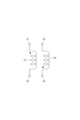
- FIG. 2 is an equivalent circuit diagram of the coil device 100.
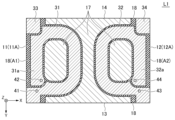
- FIG. 3 is a schematic plan view showing the shape of the conductor pattern formed on the conductor layer L1.
- FIG. 4 is a schematic plan view showing the shape of the conductor pattern formed on the conductor layer L2.
- FIG. 5 is a schematic plan view showing the shape of the conductor pattern formed on the conductor layer L3.
- FIG. 6 is a schematic plan view showing the shape of a conductor bump formed on the conductor layer L4.
- FIG. 7 is a schematic plan view showing the shape of a conductor bump formed on the conductor layer L4 according to a first modified example.
- FIG. 1 is a schematic perspective view for explaining a structure of a coil component 100 according to an embodiment of the technology disclosed herein.
- FIG. 2 is an equivalent circuit diagram of the coil device 100.
- FIG. 3 is a schematic plan view showing the
- FIG. 8 is a schematic plan view showing the shape of a conductor pattern formed on the conductor layer L1 according to a second modified example.
- FIG. 9 is a schematic plan view showing the shape of a conductor pattern formed on the conductor layer L2 according to a second modified example.
- FIG. 10 is a schematic plan view showing the shape of a conductor pattern formed on the conductor layer L3 according to a second modified example.
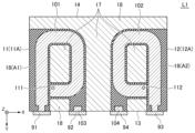
- FIG. 11 is a schematic plan view showing the shape of a conductor pattern formed on the conductor layer L1 according to a third modified example.
- FIG. 12 is a schematic plan view showing the shape of a conductor pattern formed on the conductor layer L2 according to a third modified example.
- FIG. 13 is a schematic plan view showing the shape of a conductor pattern formed on the conductor layer L3 according to a third modified example.
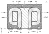
- FIG. 14 is a schematic plan view showing the shape of a conductor pattern formed on the conductor layer L1 according to a fourth modified example.
- FIG. 15 is a schematic plan view showing the shape of a conductor pattern formed on the conductor layer L2 according to a fourth modified example.
- FIG. 16 is a schematic plan view showing the shape of a conductor pattern formed on the conductor layer L3 according to a fourth modified example.
- FIG. 1 is a schematic perspective view for explaining the structure of an electronic component (coil component 100) according to one embodiment of the technology disclosed herein.
- FIG. 2 is an equivalent circuit diagram of coil component 100.
- the coil component 100 is a four-terminal chip component, and includes an element body 10 and two coils C1 and C2 embedded in the element body 10.
- the element body 10 has surfaces 11 and 12 that form a YZ plane and are located opposite each other, surfaces 13 and 14 that form an XZ plane and are located opposite each other, and a mounting surface 15 and a top surface 16 (opposing surfaces that face the mounting surface) that form an XY plane and are located opposite each other.
- the mounting surface 15 is the surface that faces the circuit board when mounted, and four terminal electrodes 21 to 24 are exposed.
- the terminal electrode 24 is not shown in FIG. 1.
- the X direction is the longitudinal direction
- the Y direction is the transverse direction.
- the terminal electrodes 21 and 22 are adjacent to each other in the Y direction, and the terminal electrodes 23 and 24 are adjacent to each other in the Y direction.
- the terminal electrodes 21 and 23 are adjacent to each other in the X direction, and the terminal electrodes 22 and 24 are adjacent to each other in the X direction.
- the element body 10 is embedded with multiple conductor layers L1 to L4 stacked in the Z direction, with coils C1 and C2 formed by conductor patterns located on conductor layers L1 to L3, and terminal electrodes 21 to 24 formed by conductor bumps located on conductor layer L4.
- the axial directions of coils C1 and C2 are both in the Z direction. Furthermore, coils C1 and C2 are arranged in the longitudinal direction, the X direction.
- Figures 3 to 6 are schematic plan views showing the shapes of the conductor patterns or conductor bumps formed on the conductor layers L1 to L4, respectively.
- the conductor patterns provided on the conductor layer L1 include coil patterns 31, 32 and dummy patterns 33, 34.
- the coil patterns 31, 32 are conductor patterns that wrap around for approximately one turn, and one end of each is disposed at a position that overlaps with the terminal electrodes 22, 24, respectively, in a plan view seen from the Z direction.
- the dummy patterns 33, 34 are provided independently of the coil patterns 31, 32, and are disposed at a position that overlaps with the terminal electrodes 21, 23, respectively, in a plan view seen from the Z direction.
- One end and the other end of the coil pattern 31 are connected to the upper conductor layer L2 via via conductors 41, 42.
- One end and the other end of the coil pattern 32 are connected to the upper conductor layer L2 via via conductors 43, 44.
- the conductor patterns provided on the conductor layer L2 include coil patterns 51 and 52, dummy patterns 53 and 54, and connection patterns 55 and 56.
- the coil patterns 51 and 52 are conductor patterns that wrap around for about one turn.
- One end of the coil patterns 51 and 52 is connected to the other end of the coil patterns 31 and 32 via via conductors 42 and 44, respectively.
- the dummy patterns 53 and 54 are provided independently of the coil patterns 51 and 52, and are arranged at positions that overlap the terminal electrodes 21 and 23, respectively, in a plan view seen from the Z direction.
- the connection patterns 55 and 56 are provided independently of the coil patterns 51 and 52, and are arranged at positions that overlap the terminal electrodes 22 and 24, respectively, in a plan view seen from the Z direction.
- the connection patterns 55 and 56 are connected to one end of the coil patterns 31 and 32 via via conductors 41 and 43, respectively.
- the conductor pattern provided on the conductor layer L3 includes coil patterns 71, 72 and connection patterns 73, 74.
- the coil patterns 71, 72 are conductor patterns that wrap around for approximately one turn.
- One end of the coil patterns 71, 72 is connected to the other end of the coil patterns 51, 52 via via conductors 62, 64, respectively.
- the other ends of the coil patterns 71, 72 are arranged at positions that overlap the terminal electrodes 21, 23, respectively, in a plan view seen from the Z direction.
- the connection patterns 73, 74 are provided independently of the coil patterns 71, 72, and are arranged at positions that overlap the terminal electrodes 22, 24, respectively, in a plan view seen from the Z direction.
- the connection patterns 73, 74 are connected to the connection patterns 55, 56 via via conductors 61, 63, respectively.
- the conductor bumps provided on the conductor layer L4 include conductor bumps B1 to B4.
- Conductor bumps B1 to B4 are connected to the other end of coil pattern 71, connection pattern 73, the other end of coil pattern 72, and connection pattern 74 via via conductors 81 to 84, respectively.
- the surfaces exposed from the base body 10 form terminal electrodes 21 to 24.
- coil patterns 31, 51, 71 are connected in series between terminal electrodes 21, 22, thereby forming coil C1.
- the portions (31a, 51a, 71a) of coil patterns 31, 51, 71 that are arranged on the surface 11 side of the element body in the X direction are sometimes referred to as the first outer periphery.
- Coil patterns 32, 52, 72 are connected in series between terminal electrodes 23, 24, thereby forming coil C2.
- the portions (32a, 52a, 72a) of coil patterns 32, 52, 72 that are arranged on the surface 12 side of the element body in the X direction are sometimes referred to as the second outer periphery.
- the winding direction of coil C1 starting from terminal electrode 21 is opposite to the winding direction of coil C2 starting from terminal electrode 23. Therefore, for example, when terminal electrodes 21 and 23 are connected to a pair of differential signal lines, and terminal electrodes 22 and 24 are connected to a power supply circuit, the differential components (signal components) flowing through the differential signal lines are prevented from flowing into the power supply circuit by coil component 100, while the DC power supply components pass through coil component 100.
- the base body 10 includes a magnetic portion 17 made of a magnetic material and a non-magnetic portion 18 made of a non-magnetic material.
- the magnetic portion 17 is made of a composite magnetic member containing a metal magnetic filler made of a magnetic material such as iron (Fe) or permalloy and a resin binder.
- the non-magnetic portion 18 is made of a non-magnetic material containing an inorganic filler such as silica and a resin binder. All of the conductor patterns formed on the conductor layers L1 to L3 are in contact with the non-magnetic portion 18, but are not in contact with the magnetic portion 17.
- each of the conductor patterns formed on the conductor layers L1 to L3 is covered by the magnetic portion 17 via the non-magnetic portion 18.
- the side surface of the conductor bump formed on the conductor layer L4 may also be covered by the non-magnetic portion 18.
- the outer regions of the coils C1 and C2 in the X direction are all made of nonmagnetic parts 18.
- the surface region A1 located between the coil C1 and the coil projection surface 11A overlapping the coil C1 as viewed from the X direction on the surface 11 of the element body 10 and the coil projection surface 12A overlapping the coil C2 as viewed from the X direction on the surface 12 of the element body 10 and the coil projection surface 12A overlapping the coil C2 as viewed from the X direction on the surface 12 of the element body 10 is all made of nonmagnetic parts 18.
- the volume of the nonmagnetic portion 18 is unlikely to affect the characteristics (e.g., inductance) of the coils C1 and C2. This reduces the difference in the characteristic value (inductance value in this case) between the coils C1 and C2 caused by manufacturing variations.
- the entire surface regions A1, A2 are made of nonmagnetic parts 18. It is sufficient that the coil projection surface 11A of the surface 11 of the element body 10, which overlaps with the coil C1 when viewed from the X direction, is made of nonmagnetic parts 18, and the coil projection surface 12A of the surface 12 of the element body 10, which overlaps with the coil C2 when viewed from the X direction, is made of nonmagnetic parts 18. In other words, as long as the magnetic parts 17 are not exposed on the coil projection surfaces 11A, 12A, it is acceptable for magnetic parts 17 to be included in part of the surface regions A1, A2.
- the surface region A5 of the base body 10 that constitutes the mounting surface 15 may be entirely made of the magnetic part 17.
- the support region A6 of the base body 10 that is located between the coils C1, C2 and the top surface 16 may be entirely made of the magnetic part 17.
- the surface regions A1, A2 of the base body 10 located on the outer side of the coils C1, C2 in the X direction are made of nonmagnetic parts 18, making it possible to reduce the difference in inductance value between the coils C1, C2 due to manufacturing variations.
- the nonmagnetic parts 18 may be provided in the surface region A5 of the base body 10 constituting the mounting surface 15, which overlaps with the surface regions A1, A2 in a plan view seen from the Z direction. This makes it possible to further reduce the difference in inductance value between the coils C1, C2.
- FIGS. 8 to 10 are schematic plan views showing the shapes of the conductor patterns formed on the conductor layers L1 to L3 according to the second modified example.
- the surface region A3 located between the coil projection surface 13A overlapping the coils C1 and C2 when viewed from the Y direction and the coils C1 and C2 on the surface 13 of the element body 10 is entirely made of nonmagnetic parts 18, and the surface region A4 located between the coil projection surface 14A overlapping the coils C1 and C2 when viewed from the Y direction and the coils C1 and C2 on the surface 14 of the element body 10 is entirely made of nonmagnetic parts 18.
- the coil projection surfaces 13A and 14A overlapping the coils C1 and C2 are made of nonmagnetic parts 18, so that the volume of the magnetic parts 17 in the surface regions A3 and A4 does not change even if the dicing position is shifted in the Y direction, and it is possible to reduce the characteristic difference between the individual coil components 100.
- Figures 11 to 13 are schematic plan views showing the shapes of the conductor patterns formed on the conductor layers L1 to L3 according to the third modified example.
- the terminal electrodes 91 to 94 are all exposed on the surface 13.
- the surface 13 that is horizontal to the stacking direction constitutes the mounting surface.
- the conductor patterns provided on the conductor layer L1 include coil patterns 101, 102 and dummy patterns 103, 104.
- the coil patterns 101, 102 are conductor patterns that wrap around for approximately one turn, and one end of each is connected to the terminal electrodes 91, 93, respectively.
- the dummy patterns 103, 104 are provided independently of the coil patterns 101, 102, and are connected to the terminal electrodes 92, 94, respectively.
- the conductor patterns provided on the conductor layer L2 include coil patterns 121, 122 and dummy patterns 123 to 126.
- the coil patterns 121, 122 are conductor patterns that wrap around for about one turn.
- One end of the coil patterns 121, 122 is connected to the other end of the coil patterns 101, 102 via via conductors 111, 112, respectively.
- the dummy patterns 123 to 126 are provided independently of the coil patterns 121, 122.
- the dummy patterns 123, 124 are connected to the terminal electrodes 91, 93, respectively, and are arranged at positions overlapping one end of the coil patterns 121, 122, respectively, in a plan view seen from the Z direction.
- the dummy patterns 125, 126 are connected to the terminal electrodes 92, 94, respectively, and are arranged at positions overlapping the dummy patterns 103, 104, respectively, in a plan view seen from the Z direction.
- the conductor patterns provided on the conductor layer L3 include coil patterns 141, 142 and dummy patterns 143, 144.
- the coil patterns 141, 142 are conductor patterns that wrap around for approximately one turn.
- One end of the coil patterns 141, 142 is connected to the other end of the coil patterns 121, 122 via via conductors 131, 132, respectively.
- the other ends of the coil patterns 141, 142 are connected to terminal electrodes 92, 94, respectively.
- the dummy patterns 143, 144 are provided independently of the coil patterns 141, 142, are connected to the terminal electrodes 91, 93, respectively, and are positioned so as to overlap with the dummy patterns 123, 124, respectively, in a plan view seen from the Z direction.
- coil patterns 101, 121, and 141 are connected in series between terminal electrodes 91 and 92, thereby forming coil C1. Furthermore, coil patterns 102, 122, and 142 are connected in series between terminal electrodes 93 and 94, thereby forming coil C2.
- the winding direction of coil C1 starting from terminal electrode 91 is opposite to the winding direction of coil C2 starting from terminal electrode 93.
- the base body 10 also includes a magnetic portion 17 made of a magnetic material and a non-magnetic portion 18 made of a non-magnetic material. Most of the inner diameter region surrounded by the coils C1 and C2 and most of the outer region located radially outward of the coils C1 and C2 are made of the magnetic portion 17. And, in the example shown in FIGS. 11 to 13, the surface regions A1 and A2 located outward in the X direction of the coils C1 and C2 are all made of the non-magnetic portion 18.
- Figures 14 to 16 are schematic plan views showing the shapes of the conductor patterns formed on the conductor layers L1 to L3 according to the fourth modified example.
- the coil projection surface 13A overlapping the coils C1, C2 when viewed from the Y direction and the surface region A3 located between the coils C1, C2 are entirely made of nonmagnetic parts 18, and on the surface 14 of the element body 10, the coil projection surface 14A overlapping the coils C1, C2 when viewed from the Y direction and the surface region A4 located between the coils C1, C2 are entirely made of nonmagnetic parts 18.
- the volume of the magnetic parts 17 in the surface regions A3, A4 does not change even if the dicing position is shifted in the Y direction, so that it is possible to reduce the characteristic differences between the individual coil components 100.
- An electronic component comprises a base body, first and second coils embedded in the base body, with a first direction as an axial direction and arranged in a second direction perpendicular to the first direction, first and second terminal electrodes exposed from the base body and connected respectively to one end and the other end of the first coil, and third and fourth terminal electrodes exposed from the base body and connected respectively to one end and the other end of the second coil, the base body including a magnetic portion made of a magnetic material and a non-magnetic portion made of a non-magnetic material, the surface of the base body including first and second surfaces facing in the second direction, the first coil projection surface of the first surface overlapping at least the first coil when viewed from the second direction exposes the non-magnetic portion without exposing the magnetic portion, and the second coil projection surface of the second surface overlapping at least the second coil when viewed from the second direction exposes the non-magnetic portion without exposing the magnetic portion.
- the first surface region of the element body located between the first coil projection surface on the first surface and the first coil may be formed of a non-magnetic portion without a magnetic portion
- the second surface region of the element body located between the second coil projection surface on the second surface and the second coil may be formed of a non-magnetic portion without a magnetic portion.
- the surface of the body has a mounting surface and an opposing surface that face each other in the first direction, the mounting surface is formed so that the first to fourth terminal electrodes are exposed, and the portion of the mounting surface that overlaps with the first and second surface regions when viewed from the first direction may be made of a non-magnetic portion. This makes it possible to further reduce the difference in inductance value between the first and second coils.
- the surface of the body further includes third and fourth surfaces that face each other in a third direction perpendicular to the first and second directions, and the third surface may have a third coil projection surface that overlaps at least the first and second coils when viewed from the third direction exposing the non-magnetic portion without exposing the magnetic portion, and the fourth surface may have a fourth coil projection surface that overlaps at least the first and second coils when viewed from the third direction exposing the non-magnetic portion without exposing the magnetic portion.
- the first terminal electrode and the third terminal electrode are adjacent to each other in the second direction, and the winding direction of the first coil starting from the first terminal electrode may be opposite to the winding direction of the second coil starting from the third terminal electrode. This allows the first and third terminal electrodes to be connected to a pair of differential signal lines, respectively, and the second and fourth terminal electrodes to be connected to a power supply circuit for use.
- An electronic component includes an element body, and first and second coils embedded in the element body, with a first direction as an axial direction and arranged in a second direction perpendicular to the first direction, the element body includes a magnetic portion made of a magnetic material and a non-magnetic portion made of a non-magnetic material, the surface of the element body includes first and second surfaces facing in the second direction, the first coil has a first outer periphery disposed on the first surface side of the element body in the second direction, the second coil has a second outer periphery disposed on the second surface side of the element body in the second direction, the non-magnetic portion is disposed between the first outer periphery and the first surface without a magnetic portion, and the non-magnetic portion is disposed between the second outer periphery and the second surface without a magnetic portion.
Landscapes
- Engineering & Computer Science (AREA)
- Power Engineering (AREA)
- Microelectronics & Electronic Packaging (AREA)
- Coils Or Transformers For Communication (AREA)
Priority Applications (2)
| Application Number | Priority Date | Filing Date | Title |
|---|---|---|---|
| CN202480026938.2A CN120981870A (zh) | 2023-04-21 | 2024-04-08 | 电子部件 |
| JP2025515169A JPWO2024219267A1 (https=) | 2023-04-21 | 2024-04-08 |
Applications Claiming Priority (2)
| Application Number | Priority Date | Filing Date | Title |
|---|---|---|---|
| JP2023-069917 | 2023-04-21 | ||
| JP2023069917 | 2023-04-21 |
Publications (1)
| Publication Number | Publication Date |
|---|---|
| WO2024219267A1 true WO2024219267A1 (ja) | 2024-10-24 |
Family
ID=93152340
Family Applications (1)
| Application Number | Title | Priority Date | Filing Date |
|---|---|---|---|
| PCT/JP2024/014223 Ceased WO2024219267A1 (ja) | 2023-04-21 | 2024-04-08 | 電子部品 |
Country Status (3)
| Country | Link |
|---|---|
| JP (1) | JPWO2024219267A1 (https=) |
| CN (1) | CN120981870A (https=) |
| WO (1) | WO2024219267A1 (https=) |
Citations (1)
| Publication number | Priority date | Publication date | Assignee | Title |
|---|---|---|---|---|
| JP2006093603A (ja) * | 2004-09-27 | 2006-04-06 | Mitsubishi Materials Corp | 積層型コモンモードチョークコイルアレイ |
-
2024
- 2024-04-08 JP JP2025515169A patent/JPWO2024219267A1/ja active Pending
- 2024-04-08 WO PCT/JP2024/014223 patent/WO2024219267A1/ja not_active Ceased
- 2024-04-08 CN CN202480026938.2A patent/CN120981870A/zh active Pending
Patent Citations (1)
| Publication number | Priority date | Publication date | Assignee | Title |
|---|---|---|---|---|
| JP2006093603A (ja) * | 2004-09-27 | 2006-04-06 | Mitsubishi Materials Corp | 積層型コモンモードチョークコイルアレイ |
Also Published As
| Publication number | Publication date |
|---|---|
| JPWO2024219267A1 (https=) | 2024-10-24 |
| CN120981870A (zh) | 2025-11-18 |
Similar Documents
| Publication | Publication Date | Title |
|---|---|---|
| KR101075318B1 (ko) | 적층형 트랜스 부품 | |
| CN112289540B (zh) | 电感器 | |
| JP7139666B2 (ja) | コイル部品 | |
| JP7452507B2 (ja) | インダクタ | |
| WO2020110692A1 (ja) | コモンモードノイズフィルタ | |
| US11521787B2 (en) | Coil component | |
| US20230317358A1 (en) | Coil component | |
| CN116052974A (zh) | 线圈零件 | |
| JP2012169410A (ja) | コイル部品 | |
| WO2024219267A1 (ja) | 電子部品 | |
| US20230253141A1 (en) | Common mode filter | |
| JP7151268B2 (ja) | コイル部品 | |
| JP2012182286A (ja) | コイル部品 | |
| US20230245813A1 (en) | Electronic component | |
| JP6547655B2 (ja) | コイル部品 | |
| JP7441647B2 (ja) | コイルユニットのコイル構造及びトランス | |
| WO2024241912A1 (ja) | 電子部品 | |
| US20250125077A1 (en) | Coil component | |
| US20250104898A1 (en) | Coil component | |
| JP2024154856A (ja) | 電子部品 | |
| WO2025069662A1 (ja) | 電子部品 | |
| WO2024070406A1 (ja) | コイル部品 | |
| WO2025197462A1 (ja) | 電子部品 | |
| US20240145161A1 (en) | Inductor component | |
| JP2005109082A (ja) | コイル部品 |
Legal Events
| Date | Code | Title | Description |
|---|---|---|---|
| 121 | Ep: the epo has been informed by wipo that ep was designated in this application |
Ref document number: 24792542 Country of ref document: EP Kind code of ref document: A1 |
|
| WWE | Wipo information: entry into national phase |
Ref document number: 2025515169 Country of ref document: JP |
|
| NENP | Non-entry into the national phase |
Ref country code: DE |
|
| 122 | Ep: pct application non-entry in european phase |
Ref document number: 24792542 Country of ref document: EP Kind code of ref document: A1 |