WO2024219244A1 - 半導体装置 - Google Patents
半導体装置 Download PDFInfo
- Publication number
- WO2024219244A1 WO2024219244A1 PCT/JP2024/013901 JP2024013901W WO2024219244A1 WO 2024219244 A1 WO2024219244 A1 WO 2024219244A1 JP 2024013901 W JP2024013901 W JP 2024013901W WO 2024219244 A1 WO2024219244 A1 WO 2024219244A1
- Authority
- WO
- WIPO (PCT)
- Prior art keywords
- island
- recess
- semiconductor device
- resin
- thickness direction
- Prior art date
- Legal status (The legal status is an assumption and is not a legal conclusion. Google has not performed a legal analysis and makes no representation as to the accuracy of the status listed.)
- Ceased
Links
Images


Classifications
-
- H—ELECTRICITY
- H10—SEMICONDUCTOR DEVICES; ELECTRIC SOLID-STATE DEVICES NOT OTHERWISE PROVIDED FOR
- H10W—GENERIC PACKAGES, INTERCONNECTIONS, CONNECTORS OR OTHER CONSTRUCTIONAL DETAILS OF DEVICES COVERED BY CLASS H10
- H10W72/00—Interconnections or connectors in packages
-
- H—ELECTRICITY
- H10—SEMICONDUCTOR DEVICES; ELECTRIC SOLID-STATE DEVICES NOT OTHERWISE PROVIDED FOR
- H10W—GENERIC PACKAGES, INTERCONNECTIONS, CONNECTORS OR OTHER CONSTRUCTIONAL DETAILS OF DEVICES COVERED BY CLASS H10
- H10W74/00—Encapsulations, e.g. protective coatings
Definitions
- the present invention relates to a semiconductor device.
- Patent Document 1 discloses an example of a conventional semiconductor device.
- the semiconductor device disclosed in this document comprises a first lead, a semiconductor element, and a sealing resin.
- the first lead comprises an island portion and a terminal portion.
- the semiconductor element is mounted on the island portion.
- the sealing resin covers a part of the island portion and the semiconductor element.
- the island portion is large compared to the terminal portion. For this reason, the position of the island portion may be unintentionally shifted during the manufacturing process of the semiconductor device. If the sealing resin is formed with the island portion shifted, there is a concern that, for example, the thickness of the sealing resin may not be adequately secured.
- An object of the present disclosure is to provide a semiconductor device that is an improvement over conventional semiconductor devices.
- an object of the present disclosure is to provide a semiconductor device that can suppress misalignment between the sealing resin and the island portion.
- the semiconductor device provided by the first aspect of the present disclosure includes a first lead having an island portion, a semiconductor element mounted on the island portion, and a sealing resin covering at least a portion of the island portion and the semiconductor element.
- the island portion has an island main surface facing a first side in the thickness direction and on which the semiconductor element is mounted, an island back surface facing a second side in the thickness direction, a first side surface facing a first side in a first direction intersecting the thickness direction, and an island recess recessed from the island back surface to the first side in the thickness direction and from the first side surface to the second side in the first direction.
- the sealing resin has a resin back surface facing the second side in the thickness direction, and a resin recess recessed from the resin back surface to the first side in the thickness direction. When viewed in the thickness direction, at least a portion of the resin recess is accommodated in the island recess.
- the above configuration makes it possible to prevent misalignment between the sealing resin and the island portion.
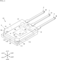
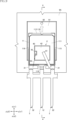
- FIG. 1 is a perspective view showing a semiconductor device according to a first embodiment of the present disclosure.
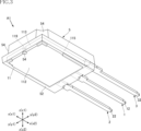
- FIG. 2 is a perspective view showing the semiconductor device according to the first embodiment of the present disclosure.
- FIG. 3 is a perspective view showing the semiconductor device according to the first embodiment of the present disclosure.
- FIG. 4 is a perspective view showing the semiconductor device according to the first embodiment of the present disclosure.
- FIG. 5 is a plan view showing the semiconductor device according to the first embodiment of the present disclosure.
- FIG. 6 is a bottom view showing the semiconductor device according to the first embodiment of the present disclosure.
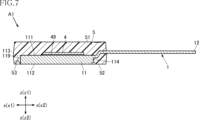
- FIG. 7 is a cross-sectional view taken along line VII-VII in FIG.
- FIG. 8 is a partially enlarged cross-sectional view showing the semiconductor device according to the first embodiment of the present disclosure.
- FIG. 1 is a perspective view showing a semiconductor device according to a first embodiment of the present disclosure.
- FIG. 2 is a perspective view showing the semiconductor device according to the first embodiment of the present disclosure.
- FIG. 3 is
- FIG. 9 is a partial plan view showing an example of a method for manufacturing a semiconductor device according to the first embodiment of the present disclosure.
- FIG. 10 is a cross-sectional view taken along line XX in FIG.
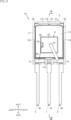
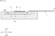
- FIG. 11 is a cross-sectional view showing an example of the method for manufacturing the semiconductor device according to the first embodiment of the present disclosure.
- FIG. 12 is a cross-sectional view showing an example of a method for manufacturing a semiconductor device according to the first embodiment of the present disclosure.
- FIG. 13 is a cross-sectional view showing an example of a method for manufacturing a semiconductor device according to the first embodiment of the present disclosure.
- FIG. 14 is a partial enlarged cross-sectional view showing a first modified example of the semiconductor device according to the first embodiment of the present disclosure.
- FIG. 10 is a cross-sectional view taken along line XX in FIG.
- FIG. 11 is a cross-sectional view showing an example of the method for manufacturing the semiconductor device according to the first embodiment of the present disclosure.
- FIG. 15 is a partial enlarged cross-sectional view showing a second modified example of the semiconductor device according to the first embodiment of the present disclosure.
- FIG. 16 is a plan view showing a third modified example of the semiconductor device according to the first embodiment of the present disclosure.
- FIG. 17 is a plan view showing a semiconductor device according to the second embodiment of the present disclosure.
- FIG. 18 is a plan view showing a semiconductor device according to a third embodiment of the present disclosure.
- an object A is formed on an object B" and “an object A is formed on an object B” include “an object A is formed directly on an object B” and “an object A is formed on an object B with another object interposed between the object A and the object B” unless otherwise specified.
- an object A is disposed on an object B” and “an object A is disposed on an object B” include “an object A is disposed directly on an object B” and “an object A is disposed on an object B with another object interposed between the object A and the object B" unless otherwise specified.
- an object A is located on an object B includes “an object A is located on an object B in contact with an object B” and “an object A is located on an object B with another object interposed between the object A and the object B” unless otherwise specified.
- an object A overlaps an object B when viewed in a certain direction includes “an object A overlaps the entire object B” and “an object A overlaps a part of an object B.”
- a surface A faces in direction B is not limited to the case where the angle of surface A with respect to direction B is 90 degrees, but also includes the case where surface A is tilted with respect to direction B.
- First embodiment: 1 to 8 show a semiconductor device according to a first embodiment of the present disclosure.
- a semiconductor device A1 of this embodiment includes a first lead 1, a second lead 2, a third lead 3, a semiconductor element 4, a sealing resin 5, and conductive members 61 and 62.
- the sealing resin 5 is shown by imaginary lines in Fig. 2 and Figs. 4 to 6.
- one direction is referred to as the z direction, the first side in the z direction as the z1 side, and the second side opposite the first side in the z direction as the z2 side.
- one direction perpendicular to the z direction is referred to as the x direction, the first side in the x direction as the x1 side, and the second side opposite the x1 side as the x2 side.
- the direction perpendicular to the z direction and the x direction is referred to as the y direction, the first side in the y direction as the y1 side, and the second side opposite the y1 side as the y2 side.
- the z direction corresponds to the thickness direction
- the x direction corresponds to the first direction in this disclosure
- the y direction corresponds to the second direction in this disclosure.
- the first lead 1 is a portion that supports the semiconductor element 4.
- the first lead 1 is also electrically connected to a first electrode 41 of the semiconductor element 4, which will be described later.
- the first lead 1 contains, for example, Cu (copper), Ni (nickel), Fe (iron), and alloys thereof.
- a plating layer (not shown) containing, for example, Ag (silver), Ni (nickel), Pd (palladium), etc. may be formed in an appropriate location on the surface of the first lead 1.
- the first lead 1 has an island portion 11 and a first terminal portion 12.
- the island portion 11 has an island main surface 111, an island back surface 112, side surfaces 113, 114, 115, 116, and an island recess 119.
- the island main surface 111 faces the z1 side in the z direction.
- the island back surface 112 faces the z2 side in the z direction.
- Side 113 is located between island main surface 111 and island back surface 112 in the z direction, and faces the x1 side in the x direction.
- side 113 corresponds to the first side in this disclosure.
- Side 114 is located between island main surface 111 and island back surface 112 in the z direction, and faces the x2 side in the x direction.
- Side 115 is located between island main surface 111 and island back surface 112 in the z direction, and faces the y1 side in the y direction.
- Side 116 is located between island main surface 111 and island back surface 112 in the z direction, and faces the y2 side in the y direction.
- the island recess 119 is recessed from the island back surface 112 toward the z1 side in the z direction, and from the side surface 113 toward the x2 side in the x direction.
- the specific shape of the island recess 119 is not limited in any way.
- the island recess 119 reaches the island back surface 112 and the island main surface 111.
- the island recess 119 has a shape that has a concave surface that curves toward the x2 side in the x direction.
- this concave surface is, for example, an arc shape.
- the island recess 119 is not limited to a shape that has a concave surface, and may, for example, have a bent concave surface.
- the first terminal 12 extends from the island 11 to the x2 side in the x direction.
- the first terminal 12 is used when mounting the semiconductor device A1.
- the size of the island 11 in the y direction is greater than the size of the first terminal 12 in the y direction.
- the size of the island 11 in the z direction is greater than the size of the first terminal 12 in the z direction.
- the first terminal 12 has a bent portion.
- the second lead 2 is electrically connected to a second electrode 42 of the semiconductor element 4 described below.
- the second lead 2 contains, for example, Cu (copper), Ni (nickel), Fe (iron), and alloys thereof.
- a plating layer (not shown) containing, for example, Ag (silver), Ni (nickel), Pd (palladium), etc. may be formed in an appropriate location on the surface of the second lead 2.
- the specific configuration of the second lead 2 is not limited in any way, and in this embodiment, the second lead 2 has a bonding portion 21 and a second terminal portion 22.
- the bonding portion 21 is disposed on the x2 side of the island portion 11 in the x direction, and is located on the y1 side of the first terminal portion 12 in the y direction.
- the bonding portion 21 has a shape with the y direction as its longitudinal direction.
- the second terminal portion 22 extends from the bonding portion 21 to the x2 side in the x direction, and is located on the y1 side in the y direction relative to the first terminal portion 12.
- the second terminal portion 22 is used when mounting the semiconductor device A1.
- the size of the bonding portion 21 in the y direction is larger than the size of the second terminal portion 22 in the y direction.
- the size of the bonding portion 21 in the z direction is the same as the size of the second terminal portion 22 in the z direction.
- the third lead 3 is electrically connected to a third electrode 43 of the semiconductor element 4 described below.
- the third lead 3 contains, for example, Cu (copper), Ni (nickel), Fe (iron) and alloys thereof.
- a plating layer (not shown) containing, for example, Ag (silver), Ni (nickel), Pd (palladium) or the like may be formed at an appropriate location on the surface of the third lead 3.
- the specific configuration of the third lead 3 is not limited in any way, and in this embodiment, it has a bonding portion 31 and a third terminal portion 32.
- the bonding portion 31 is disposed on the x2 side of the island portion 11 in the x direction, and is located on the y2 side of the first terminal portion 12 in the y direction.
- the bonding portion 31 has a shape with the y direction as its longitudinal direction.
- the third terminal portion 32 extends from the bonding portion 31 to the x2 side in the x direction, and is located on the y2 side in the y direction relative to the first terminal portion 12.
- the third terminal portion 32 is used when mounting the semiconductor device A1.
- the size of the bonding portion 31 in the y direction is greater than the size of the third terminal portion 32 in the y direction.
- the size of the bonding portion 31 in the z direction is the same as the size of the third terminal portion 32 in the z direction.
- the semiconductor element 4 is an element that performs the main electrical function of the semiconductor device A1.
- the specific configuration of the semiconductor element 4 is not limited in any way, and may be, for example, a switching element, a diode, or the like.
- the semiconductor element 4 is, for example, a transistor such as a vertical-structure MOSFET (Metal-Oxide-Semiconductor Field-Effect Transistor) or an IGBT (Insulated Gate Bipolar Transistor).
- MOSFET Metal-Oxide-Semiconductor Field-Effect Transistor
- IGBT Insulated Gate Bipolar Transistor
- the semiconductor element 4 has an element body 40, a first electrode 41, a second electrode 42 and a third electrode 43.
- the element body 40 includes a semiconductor material.
- the semiconductor material is, for example, silicon carbide (SiC).
- Other semiconductor materials that may be used include silicon (Si) or gallium nitride (GaN).
- the first electrode 41 is disposed on the z2 side of the element body 40 in the z direction.
- the first electrode 41 is conductively joined to the island main surface 111 of the island portion 11 by a conductive bonding material 49.
- the conductive bonding material 49 is not limited in any way and may be, for example, solder, Ag (silver) paste, or a sintered metal material.
- the second electrode 42 and the third electrode 43 are disposed on the z1 side of the element body 40 in the z direction. In the illustrated example, the second electrode 42 is larger than the third electrode 43.
- the semiconductor element 4 is a MOSFET
- the first electrode 41 is the drain
- the second electrode 42 is the source
- the third electrode 43 is the gate electrode.
- Conductive members 61, 62 The conductive member 61 is joined to the second electrode 42 of the semiconductor element 4 and the bonding portion 21 of the second lead 2.
- the conductive member 61 electrically connects the second electrode 42 and the second lead 2.
- the specific configuration of the conductive member 61 is not limited in any way, and various forms may be adopted, such as a wire or a strip-shaped member.
- the conductive member 61 is a strip-shaped member.
- the conductive member 61 includes, for example, Au (gold), Al (aluminum), Cu (copper), and alloys thereof.
- the conductive member 62 is bonded to the third electrode 43 of the semiconductor element 4 and the bonding portion 31 of the third lead 3.
- the conductive member 62 provides electrical conductivity between the third electrode 43 and the third lead 3.
- the specific configuration of the conductive member 62 is not limited in any way, and various forms may be adopted, such as a wire or a strip-shaped member.
- the conductive member 62 is a wire.
- the conductive member 62 includes, for example, Au (gold), Al (aluminum), Cu (copper), and alloys thereof.
- the sealing resin 5 covers parts of the first lead 1, the second lead 2, and the third lead 3, the semiconductor element 4, and the conductive members 61 and 62.
- the sealing resin 5 contains an insulating material, such as a black epoxy resin.
- the specific configuration of the sealing resin 5 is not limited in any way, and in this embodiment, the sealing resin 5 has a resin main surface 51, a resin back surface 52, a resin recess 53, and a corner recess 54.
- the resin main surface 51 faces the z1 side in the z direction.
- the resin back surface 52 faces the z2 side in the z direction.
- the island back surface 112 of the island portion 11 is exposed from the resin back surface 52.
- the resin back surface 52 and the island back surface 112 are flush with each other.
- the resin recess 53 is recessed from the resin back surface 52 toward the z1 side in the z direction. As shown in Figures 1 to 8, when viewed in the z direction, at least a portion of the resin recess 53 is housed in the island recess 119. In the illustrated example, a portion of the resin recess 53 is housed in the island recess 119, and another portion protrudes from the island recess 119 to the z1 side in the z direction. In the illustrated example, the edge of the resin recess 53 on the z2 side in the z direction and the edge of the island recess 119 on the z2 side in the z direction partially coincide with each other.
- the portion of the edge of the resin recess 53 on the z2 side in the z direction that is located on the x2 side in the x direction coincides with the edge of the island recess 119 on the z2 side in the z direction.
- the size of the resin recess 53 in the z direction is smaller than the size of the island recess 119 in the z direction.
- the specific shape of the resin recess 53 is not limited in any way.
- the resin recess 53 has a shape in which the size of a cross section perpendicular to the z direction decreases from the z2 side toward the z1 side in the z direction, for example, a cone shape.
- the resin recess 53 may also have an elliptical cone shape, a pyramid shape, or the like. Note that the resin recess 53 does not have to have a so-called tapered shape.
- the radius of curvature of the edge of the resin recess 53 on the z2 side in the z direction and the radius of curvature of the edge of the island recess 119 on the z2 side in the z direction are approximately the same.
- the first lead 1 shown in Figures 9 and 10 is prepared.
- the specific form of the first lead 1 in the manufacturing process of the semiconductor device A1 is not limited in any way.
- the semiconductor element 4 is mounted on the first lead 1.
- the lower mold 9A constitutes the mold 9 for molding the sealing resin 5.
- the lower mold 9A has a mold main surface 91 and a mold convex portion 92.
- the mold main surface 91 is a noodle that faces the island back surface 112 of the island portion 11 during molding.
- the mold convex portion 92 protrudes from the mold main surface 91 to the z1 side in the z direction.
- the mold convex portion 92 is a portion for forming the resin recess 53 of the sealing resin 5.
- the position, shape, size, etc. of the resin recess 53 are set corresponding to the position, shape, size, etc. of the resin recess 53. In the illustrated example, the resin recess 53 is cone-shaped.
- the first lead 1 is placed on the lower mold 9A.
- the island recess 119 of the island portion 11 is brought close to the mold protrusion 92.
- the island recess 119 is brought close to the mold protrusion 92 from the z1 side in the z direction and the x2 side in the x direction, toward the z2 side in the z direction and the x1 side in the x direction.
- the island recess 119 and the mold protrusion 92 come into contact with each other.
- the island back surface 112 and the mold main surface 91 come into contact with each other.
- at least a portion of the mold protrusion 92 is accommodated in the island recess 119.
- a portion of the mold protrusion 92 protrudes from the island recess 119 to the x1 side in the x direction, and another portion of the mold protrusion 92 is accommodated in the island recess 119.
- the portion of the edge of the mold protrusion 92 on the z2 side in the z direction on the x2 side in the x direction comes into contact with the edge of the island recess 119 on the z2 side in the z direction.
- the mold 9 has a cavity 90.
- the cavity 90 is a space that is filled with a resin material to form the sealing resin 5.
- the cavity 90 is filled with a resin material, and the resin material is cured. This forms the sealing resin 5.
- the semiconductor device A1 is obtained by appropriately performing a process for removing unnecessary parts of the lead frame as described above.
- the resin recess 53 is housed in the island recess 119 when viewed in the z direction.
- the resin recess 53 is a portion recessed from the resin back surface 52 toward the z1 side in the z direction.
- the lower die 9A of the die 9 has a die protrusion 92 as shown in FIG. 13. By abutting this die protrusion 92 with the island recess 119, it is possible to set the position of the island portion 11 more accurately with respect to the die 9. Therefore, the positional deviation between the sealing resin 5 and the island portion 11 can be reduced.
- the resin recess 53 has a so-called tapered shape in which the size of the cross section perpendicular to the z direction decreases from the z2 side toward the z2 side in the z direction.
- the size of the island portion 11 in the y direction is greater than the size of the first terminal portion 12 in the y direction, and the size of the island portion 11 in the z direction is greater than the size of the first terminal portion 12 in the z direction. For this reason, the island portion 11 accounts for a large portion of the weight of the first lead 1, and is prone to misalignment known as swaying.
- the island recess 119 and the resin recess 53 are located on the opposite side of the first terminal portion 12 in the x direction. This makes it possible to reduce the swaying behavior of the island portion 11 when molding the sealing resin 5 with a die.
- FIGS. 14 to 18 show other embodiments of the present invention.
- elements that are the same as or similar to those in the above embodiment are given the same reference numerals as in the above embodiment.
- the configurations of each part in each modified example and each embodiment can be combined with each other as appropriate to the extent that no technical contradictions arise.
- First Modification of First Embodiment 14 shows a first modified example of the semiconductor device A1.
- the shape of the resin recess 53 is different from that of the semiconductor device A1 described above.
- the resin recess 53 has a constant size of a cross section perpendicular to the z direction in the portion on the z2 side in the z direction.
- the portion on the z1 side in the z direction of the resin recess 53 is formed as a hemispherical curved surface.
- This modified example also reduces the misalignment between the sealing resin 5 and the island portion 11.
- the shape of the resin recess 53 is not limited in any way.
- Second Modification of First Embodiment 15 shows a second modified example of the semiconductor device A1.
- the semiconductor device A12 of this modified example has a different configuration of the island recess 119 from the above-mentioned example.
- the island recess 119 does not reach the island main surface 111 and is spaced apart from the island main surface 111.
- a part of the side surface 113 is interposed between the island recess 119 and the island main surface 111.
- the size of the resin recess 53 in the z direction is smaller than the size of the island recess 119 in the z direction.
- This modified example also reduces the misalignment between the sealing resin 5 and the island portion 11.
- the specific configuration of the island recess 119 is not limited in any way.
- Second Modification of First Embodiment 16 shows a third modified example of the semiconductor device A1.
- the relationship between the island recess 119 and the resin recess 53 is different from that of the above-mentioned example.
- the entire resin recess 53 is accommodated in the island recess 119 when viewed in the z direction.
- the island recess 119 has a shape having a concave curved surface located on the x1 side in the x direction and two flat surfaces interposed between the concave curved surface and the side surface 113.
- This modified example also reduces the misalignment between the sealing resin 5 and the island portion 11.
- the resin recess 53 is configured so that at least a portion of it is housed in the island recess 119 when viewed in the z direction. Only a portion of the resin recess 53 may be housed in the island recess 119, or the entire resin recess 53 may be housed in the island recess 119.
- Second embodiment: 17 shows a semiconductor device according to a second embodiment of the present disclosure.
- a semiconductor device A2 according to this embodiment has an island portion 11 having a different configuration from the above-described embodiments.
- the island portion 11 has two side surfaces 118.
- the two side surfaces 118 face the x1 side in the x direction.
- the two side surfaces 118 are located on either side of the side surface 113 in the y direction.
- the two side surfaces 118 are located on the x2 side of the side surface 113 in the x direction.
- the part of the island portion 11 that includes the side surface 113 protrudes toward the x1 side in the x direction relative to the two side surfaces 118.
- This embodiment also reduces misalignment between the sealing resin 5 and the island portion 11.
- Third embodiment: 18 shows a semiconductor device according to a third embodiment of the present disclosure.
- the island portion 11 has two island recesses 119.
- One of the two island recesses 119 is recessed from the side surface 115 toward the y2 side in the y direction.
- the side surface 115 corresponds to the first side surface of the present disclosure
- the y direction corresponds to the first direction.
- the other of the two island recesses 119 is recessed from the side surface 116 toward the y1 side in the y direction.
- the side surface 116 corresponds to the first side surface of the present disclosure
- the y direction corresponds to the first direction.
- the sealing resin 5 has two resin recesses 53.
- the two resin recesses 53 are arranged apart from each other in the y direction. When viewed in the z direction, at least a portion of each of the two resin recesses 53 is individually accommodated in two island recesses 119.
- This embodiment also reduces misalignment between the sealing resin 5 and the island portion 11.
- the number and arrangement of the island recesses 119 and the resin recesses 53 are not limited in any way.
- the semiconductor device according to the present invention is not limited to the above-mentioned embodiment.
- the specific configuration of each part of the semiconductor device according to the present invention can be freely designed in various ways.
- Appendix 1 a first lead having an island portion; A semiconductor element mounted on the island portion; a sealing resin that covers at least a portion of the island portion and the semiconductor element, the island portion has an island main surface facing a first side in a thickness direction and on which the semiconductor element is mounted, an island back surface facing a second side in the thickness direction, a first side surface facing a first side in a first direction intersecting the thickness direction, and an island recess recessed from the island back surface to the first side in the thickness direction and from the first side surface to a second side in the first direction, the sealing resin has a resin back surface facing the second side in the thickness direction and a resin recessed portion recessed from the resin back surface to the first side in the thickness direction, When viewed in the thickness direction, at least a portion of the resin recess is accommodated in the island recess.
- Appendix 2 2. The semiconductor device according to claim 1, wherein a portion of the resin recess protrudes from the island recess when viewed in the thickness direction. Appendix 3. 2. The semiconductor device according to claim 1, wherein, when viewed in the thickness direction, the resin recess is entirely contained in the island recess. Appendix 4. 4. The semiconductor device according to claim 1, wherein an edge of the resin recess and an edge of the island recess are partially aligned. Appendix 5. 5. 5. The semiconductor device according to claim 1, wherein the back surface of the island and the back surface of the resin are flush with each other. Appendix 6. 6. 6.
- the resin recess has a shape in which the size of a cross section perpendicular to the thickness direction decreases as the cross section moves from the second side to the first side in the thickness direction.
- Appendix 7. The semiconductor device according to claim 6, wherein the resin recess is cone-shaped.
- Appendix 8. The semiconductor device according to claim 1, wherein the size of the resin recess in the thickness direction is smaller than the size of the island recess in the thickness direction.
- Appendix 9. 9.
- Appendix 10. 9. The semiconductor device of claim 8, wherein the island recess is spaced from the island main surface. Appendix 11. 11.
- the semiconductor element is a switching element having a first electrode conductively joined to the island portion, a second electrode provided on the first side in the thickness direction, and a third electrode for controlling a conductive state of the first electrode and the second electrode.
- Appendix 16. 16 The semiconductor device of claim 15, further comprising a second lead electrically connected to the second electrode. Appendix 17.
- the island portion has an island main surface facing a first side in a thickness direction and on which the semiconductor element is mounted, an island back surface facing a second side in the thickness direction, a first side surface facing a first side in a first direction intersecting the thickness direction, and an island recess recessed from the island back surface to the first side in the thickness direction and from the first side surface to a second side in the first direction, the mold has a mold main surface facing the island main surface and a mold protrusion protruding from the mold main surface, In the step of forming the sealing resin, the island recess and the mold protrusion are brought into contact with each other.
Landscapes
- Structures Or Materials For Encapsulating Or Coating Semiconductor Devices Or Solid State Devices (AREA)
Priority Applications (1)
| Application Number | Priority Date | Filing Date | Title |
|---|---|---|---|
| JP2025515156A JPWO2024219244A1 (https=) | 2023-04-21 | 2024-04-04 |
Applications Claiming Priority (2)
| Application Number | Priority Date | Filing Date | Title |
|---|---|---|---|
| JP2023070164 | 2023-04-21 | ||
| JP2023-070164 | 2023-04-21 |
Publications (1)
| Publication Number | Publication Date |
|---|---|
| WO2024219244A1 true WO2024219244A1 (ja) | 2024-10-24 |
Family
ID=93152872
Family Applications (1)
| Application Number | Title | Priority Date | Filing Date |
|---|---|---|---|
| PCT/JP2024/013901 Ceased WO2024219244A1 (ja) | 2023-04-21 | 2024-04-04 | 半導体装置 |
Country Status (2)
| Country | Link |
|---|---|
| JP (1) | JPWO2024219244A1 (https=) |
| WO (1) | WO2024219244A1 (https=) |
Citations (8)
| Publication number | Priority date | Publication date | Assignee | Title |
|---|---|---|---|---|
| JPH02290032A (ja) * | 1989-12-14 | 1990-11-29 | Hitachi Ltd | レジンモールド型半導体装置の製造方法 |
| JPH06314765A (ja) * | 1993-04-30 | 1994-11-08 | Nec Corp | リードフレーム、半導体装置および半導体装置の製造方法 |
| JPH08204099A (ja) * | 1995-01-31 | 1996-08-09 | Rohm Co Ltd | 半導体装置の構造及び形成方法 |
| JP2010034349A (ja) * | 2008-07-30 | 2010-02-12 | Sanyo Electric Co Ltd | 半導体装置の製造方法およびリードフレーム |
| JP2010109254A (ja) * | 2008-10-31 | 2010-05-13 | Sanyo Electric Co Ltd | 半導体装置およびその製造方法 |
| JP2016082065A (ja) * | 2014-10-16 | 2016-05-16 | 新電元工業株式会社 | 半導体装置の製造方法、半導体装置、金型およびリードフレーム |
| WO2020059751A1 (ja) * | 2018-09-19 | 2020-03-26 | ローム株式会社 | 半導体装置 |
| WO2022014300A1 (ja) * | 2020-07-13 | 2022-01-20 | ローム株式会社 | 半導体装置、および半導体装置の製造方法 |
-
2024
- 2024-04-04 JP JP2025515156A patent/JPWO2024219244A1/ja active Pending
- 2024-04-04 WO PCT/JP2024/013901 patent/WO2024219244A1/ja not_active Ceased
Patent Citations (8)
| Publication number | Priority date | Publication date | Assignee | Title |
|---|---|---|---|---|
| JPH02290032A (ja) * | 1989-12-14 | 1990-11-29 | Hitachi Ltd | レジンモールド型半導体装置の製造方法 |
| JPH06314765A (ja) * | 1993-04-30 | 1994-11-08 | Nec Corp | リードフレーム、半導体装置および半導体装置の製造方法 |
| JPH08204099A (ja) * | 1995-01-31 | 1996-08-09 | Rohm Co Ltd | 半導体装置の構造及び形成方法 |
| JP2010034349A (ja) * | 2008-07-30 | 2010-02-12 | Sanyo Electric Co Ltd | 半導体装置の製造方法およびリードフレーム |
| JP2010109254A (ja) * | 2008-10-31 | 2010-05-13 | Sanyo Electric Co Ltd | 半導体装置およびその製造方法 |
| JP2016082065A (ja) * | 2014-10-16 | 2016-05-16 | 新電元工業株式会社 | 半導体装置の製造方法、半導体装置、金型およびリードフレーム |
| WO2020059751A1 (ja) * | 2018-09-19 | 2020-03-26 | ローム株式会社 | 半導体装置 |
| WO2022014300A1 (ja) * | 2020-07-13 | 2022-01-20 | ローム株式会社 | 半導体装置、および半導体装置の製造方法 |
Also Published As
| Publication number | Publication date |
|---|---|
| JPWO2024219244A1 (https=) | 2024-10-24 |
Similar Documents
| Publication | Publication Date | Title |
|---|---|---|
| US12406910B2 (en) | Packaging of a semiconductor device with a plurality of leads | |
| TWI378543B (en) | Semiconductor package having dimpled plate interconnections | |
| US20090079006A1 (en) | Semiconductor apparatus | |
| JP7594950B2 (ja) | 半導体装置 | |
| US20110163432A1 (en) | Semiconductor device and method of manufacturing the same | |
| US8581378B2 (en) | Semiconductor device and method of manufacturing the same | |
| KR101644913B1 (ko) | 초음파 용접을 이용한 반도체 패키지 및 제조 방법 | |
| US20180211930A1 (en) | Semiconductor device and method for manufacturing the same | |
| WO2024219244A1 (ja) | 半導体装置 | |
| CN114520203A (zh) | 用于半导体器件封装的接触夹 | |
| JP4694594B2 (ja) | 半導体装置 | |
| JP7460051B2 (ja) | 半導体装置 | |
| JP7824231B2 (ja) | 半導体装置の製造方法および半導体装置 | |
| JP2005311099A (ja) | 半導体装置及びその製造方法 | |
| JP2023127285A (ja) | 半導体装置 | |
| JP2007165442A (ja) | モールドパッケージ | |
| US11823985B2 (en) | Leadframe, semiconductor device, and method for manufacturing semiconductor device | |
| US20240282690A1 (en) | Semiconductor device | |
| WO2024057876A1 (ja) | 半導体装置 | |
| WO2025142395A1 (ja) | 半導体装置 | |
| WO2026014325A1 (ja) | 半導体装置 | |
| JP2025075374A (ja) | 電子装置及び実装構造体 | |
| WO2024181293A1 (ja) | 半導体装置 | |
| WO2024150668A1 (ja) | 半導体装置 | |
| JP2026034900A (ja) | 半導体装置 |
Legal Events
| Date | Code | Title | Description |
|---|---|---|---|
| 121 | Ep: the epo has been informed by wipo that ep was designated in this application |
Ref document number: 24792519 Country of ref document: EP Kind code of ref document: A1 |
|
| ENP | Entry into the national phase |
Ref document number: 2025515156 Country of ref document: JP Kind code of ref document: A |
|
| WWE | Wipo information: entry into national phase |
Ref document number: 2025515156 Country of ref document: JP |
|
| NENP | Non-entry into the national phase |
Ref country code: DE |
|
| 122 | Ep: pct application non-entry in european phase |
Ref document number: 24792519 Country of ref document: EP Kind code of ref document: A1 |