WO2024219184A1 - 放熱部材、放熱部材の製造方法および真空バルブ - Google Patents
放熱部材、放熱部材の製造方法および真空バルブ Download PDFInfo
- Publication number
- WO2024219184A1 WO2024219184A1 PCT/JP2024/012718 JP2024012718W WO2024219184A1 WO 2024219184 A1 WO2024219184 A1 WO 2024219184A1 JP 2024012718 W JP2024012718 W JP 2024012718W WO 2024219184 A1 WO2024219184 A1 WO 2024219184A1
- Authority
- WO
- WIPO (PCT)
- Prior art keywords
- layer
- heat dissipation
- coating layer
- dissipation member
- copper
- Prior art date
- Legal status (The legal status is an assumption and is not a legal conclusion. Google has not performed a legal analysis and makes no representation as to the accuracy of the status listed.)
- Ceased
Links
Images


Classifications
-
- H—ELECTRICITY
- H10—SEMICONDUCTOR DEVICES; ELECTRIC SOLID-STATE DEVICES NOT OTHERWISE PROVIDED FOR
- H10W—GENERIC PACKAGES, INTERCONNECTIONS, CONNECTORS OR OTHER CONSTRUCTIONAL DETAILS OF DEVICES COVERED BY CLASS H10
- H10W40/00—Arrangements for thermal protection or thermal control
- H10W40/20—Arrangements for cooling
- H10W40/25—Arrangements for cooling characterised by their materials
- H10W40/255—Arrangements for cooling characterised by their materials having a laminate or multilayered structure, e.g. direct bond copper [DBC] ceramic substrates
-
- H—ELECTRICITY
- H01—ELECTRIC ELEMENTS
- H01H—ELECTRIC SWITCHES; RELAYS; SELECTORS; EMERGENCY PROTECTIVE DEVICES
- H01H1/00—Contacts
- H01H1/62—Heating or cooling of contacts
-
- H—ELECTRICITY
- H01—ELECTRIC ELEMENTS
- H01H—ELECTRIC SWITCHES; RELAYS; SELECTORS; EMERGENCY PROTECTIVE DEVICES
- H01H33/00—High-tension or heavy-current switches with arc-extinguishing or arc-preventing means
- H01H33/60—Switches wherein the means for extinguishing or preventing the arc do not include separate means for obtaining or increasing flow of arc-extinguishing fluid
- H01H33/66—Vacuum switches
- H01H33/662—Housings or protective screens
-
- H—ELECTRICITY
- H01—ELECTRIC ELEMENTS
- H01H—ELECTRIC SWITCHES; RELAYS; SELECTORS; EMERGENCY PROTECTIVE DEVICES
- H01H9/00—Details of switching devices, not covered by groups H01H1/00 - H01H7/00
- H01H9/52—Cooling of switch parts
-
- H—ELECTRICITY
- H05—ELECTRIC TECHNIQUES NOT OTHERWISE PROVIDED FOR
- H05K—PRINTED CIRCUITS; CASINGS OR CONSTRUCTIONAL DETAILS OF ELECTRIC APPARATUS; MANUFACTURE OF ASSEMBLAGES OF ELECTRICAL COMPONENTS
- H05K7/00—Constructional details common to different types of electric apparatus
- H05K7/20—Modifications to facilitate cooling, ventilating, or heating
-
- H—ELECTRICITY
- H10—SEMICONDUCTOR DEVICES; ELECTRIC SOLID-STATE DEVICES NOT OTHERWISE PROVIDED FOR
- H10W—GENERIC PACKAGES, INTERCONNECTIONS, CONNECTORS OR OTHER CONSTRUCTIONAL DETAILS OF DEVICES COVERED BY CLASS H10
- H10W40/00—Arrangements for thermal protection or thermal control
- H10W40/01—Manufacture or treatment
- H10W40/03—Manufacture or treatment of arrangements for cooling
-
- H—ELECTRICITY
- H10—SEMICONDUCTOR DEVICES; ELECTRIC SOLID-STATE DEVICES NOT OTHERWISE PROVIDED FOR
- H10W—GENERIC PACKAGES, INTERCONNECTIONS, CONNECTORS OR OTHER CONSTRUCTIONAL DETAILS OF DEVICES COVERED BY CLASS H10
- H10W40/00—Arrangements for thermal protection or thermal control
- H10W40/20—Arrangements for cooling
- H10W40/25—Arrangements for cooling characterised by their materials
- H10W40/258—Metallic materials
-
- H—ELECTRICITY
- H10—SEMICONDUCTOR DEVICES; ELECTRIC SOLID-STATE DEVICES NOT OTHERWISE PROVIDED FOR
- H10W—GENERIC PACKAGES, INTERCONNECTIONS, CONNECTORS OR OTHER CONSTRUCTIONAL DETAILS OF DEVICES COVERED BY CLASS H10
- H10W40/00—Arrangements for thermal protection or thermal control
- H10W40/20—Arrangements for cooling
- H10W40/25—Arrangements for cooling characterised by their materials
- H10W40/259—Ceramics or glasses
Definitions
- This disclosure relates to a heat dissipation member, a method for manufacturing a heat dissipation member, and a vacuum valve.
- Patent Document 1 discloses a heat dissipation material that is characterized by a substrate formed from a composite material made of ceramics and aluminum, and an anodized aluminum layer formed on at least one surface of the substrate.
- Patent Document 1 makes it possible to impart infrared radiation performance by forming a metal oxide coating on the surface of a component made of a light metal (Al, Mg), it is difficult to impart infrared radiation performance by forming a metal oxide coating on the surface of a heavy metal such as copper, which is often used as a conductive component in electrical and electronic devices.
- This disclosure discloses technology to solve the problems described above, and aims to provide a heat dissipation member that has excellent adhesion between the substrate and the coating layer and has high emissivity without reducing the conductivity of the substrate, a method for manufacturing the heat dissipation member, and a vacuum valve.
- the heat dissipation member of the present disclosure is A heat dissipation component having a base material whose main component is copper and a coating layer covering the surface of the base material, the coating layer having a ceramic layer whose main component is an oxide of a metal element having a greater ionization tendency than copper, and a diffusion layer at the interface between the base material and the coating layer in which the metal element is diffused into the copper, the metal element being zinc or nickel.
- the heat dissipation member of the present disclosure is A heat dissipation member having a base material mainly composed of copper and a coating layer covering a surface of the base material, the coating layer having a ceramic layer mainly composed of an oxide of a metal element having a higher ionization tendency than copper, and a diffusion layer in which the metal element is diffused into the copper at the interface between the base material and the coating layer,
- the coating layer has a metal layer made of the metal element between the substrate and the ceramic layer.
- a method for producing a heat dissipation member according to the present disclosure includes the steps of: The method includes the steps of forming a metal plating layer as the coating layer on the substrate, and oxidizing the metal plating layer by heat treatment to form the ceramic layer.
- the vacuum valve of the present disclosure further comprises: The heat dissipating member is provided on the surface of at least one of the fixed electrode bar and the movable electrode bar.
- the method for manufacturing the heat dissipation member, and the vacuum valve of the present disclosure It is possible to provide a heat dissipation member having excellent adhesion between a substrate and a coating layer and high emissivity without reducing the electrical conductivity of the substrate, a method for manufacturing a heat dissipation member, and a vacuum interrupter.
- FIG. 2 is a schematic cross-sectional view of a heat dissipation member according to the first embodiment.
- FIG. 4 is a schematic cross-sectional view showing another example of the coating layer according to the first embodiment.
- FIG. 3 is a schematic cross-sectional view showing an example of a crystal of a coating layer according to embodiment 1.
- FIG. 4 is a schematic cross-sectional view showing another example of crystals of the coating layer according to embodiment 1.
- FIG. 3 is a schematic cross-sectional view showing an alloy layer formed in a diffusion layer of the heat dissipation member according to the first embodiment.
- FIG. 4 is a schematic cross-sectional view showing another example of the alloy layer according to the first embodiment.
- FIG. 3 is a schematic cross-sectional view of a heat dissipation member in which a metal layer remains on a coating layer according to the first embodiment.
- FIG. 4 is a flowchart showing a manufacturing process of the heat dissipation member according to the first embodiment.
- 5A to 5C are diagrams showing configurations of a heat dissipation member according to a first embodiment of the present invention; 11A to 11C are diagrams showing configurations of examples 6 to 8 of the heat dissipation member according to the first embodiment; 1 is a diagram showing the configuration of heat dissipation members according to Comparative Examples 1 to 3; 6 is a schematic cross-sectional view of a vacuum interrupter according to a second embodiment.
- FIG. 13A to 13B are diagrams showing configurations of a heat dissipation member according to embodiment 3;
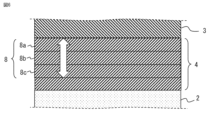
- FIG. 1 is a schematic cross-sectional view of a heat dissipation member 100 according to the first embodiment.
- the heat dissipation member 100 is made up of a copper base material 2 (hereinafter simply referred to as the base material 2 ), a coating layer 3 , and a diffusion layer 4 .
- the substrate 2 constituting the heat dissipation member 100 is preferably a copper-based material, since it has excellent thermal and electrical conductivity and is cost-effective.
- copper alloys such as brass and cupro-nickel can be used.
- pure copper is preferred, with a volume resistivity of preferably 2.5 ⁇ cm or less, and more preferably 1.8 ⁇ cm or less.
- oxygen-free copper is preferred when use in a high vacuum is anticipated. By using oxygen-free copper, it is possible to prevent a decrease in the degree of vacuum due to the release of oxygen dissolved in the copper.
- sputtering which requires a complicated vacuum process
- thermal spraying which requires an ultra-high temperature process
- a plating film made of a metal element is formed on the surface of the substrate 2, and the plating film is oxidized in air to easily form a ceramic coating layer 3 on the substrate 2.
- the coating layer 3 refers to the portion of the plating film applied to the substrate 2, and the oxidized portion of the coating layer 3 is specifically referred to as the ceramic layer.
- the entire coating layer 3 is a ceramic layer, and in other cases, only a portion of the coating layer 3 is a ceramic layer, as described below.
- the heat dissipation member 100 of the present embodiment 1 has excellent adhesion of the coating layer 3 without reducing the conductivity of the substrate 2, and has high emissivity and excellent heat dissipation properties.
- the coating layer 3 constituting the heat dissipation member 100 plays a role in improving the infrared radiation performance of the heat dissipation member 100.
- it is preferably made of a ceramic material made of a material with high emissivity.
- it is preferable that it is an oxide of a metal element that has a greater ionization tendency than copper.
- ceramic materials such as zinc oxide, silica, and nickel oxide are used.
- FIG. 2 is a schematic cross-sectional view showing another example of the coating layer 3.
- the coating layer 3 may have a laminated structure of a coating layer 3A (first coating layer) and a coating layer 3B (second coating layer) made of two different ceramic materials.
- the coating layer 3 By forming the coating layer 3 into a laminated structure of two layers, it is possible to form the coating layer 3A, which has a thermal expansion coefficient closer to that of the substrate 2 than the coating layer 3B, which is the upper layer, on the substrate 2 side, in the lower layer, and to form the coating layer 3B, which has a higher emissivity than the coating layer 3A, in the upper layer.
- the ceramic layer that is the coating layer 3 of the heat dissipation member of this embodiment is crystalline.
- the thermal conductivity inside the ceramic layer increases, and heat is efficiently transferred to the ceramic layer responsible for radiation, making it easier to improve radiation performance.
- the crystalline state of the ceramic layer can be confirmed by X-ray diffraction. When diffraction peaks due to the crystal structure are observed in the X-ray diffraction pattern, it can be confirmed as crystalline, and when only a halo pattern is observed, it can be confirmed as amorphous.
- the thickness of the coating layer 3 is preferably 0.5 ⁇ m or more and 20 ⁇ m or less, and more preferably 1 ⁇ m or more and 10 ⁇ m or less. If the thickness is less than 0.5 ⁇ m, sufficient radiation performance may not be obtained. On the other hand, if the film thickness exceeds 20 ⁇ m, the ceramic layer becomes brittle and problems such as peeling may occur during long-term use.
- FIG. 3 is a schematic cross-sectional view showing an example of a crystal particle 6 of the coating layer 3.
- FIG. 4 is a schematic cross-sectional view showing another example of the crystal grains 6 of the coating layer 3.
- the form of the ceramic layer which is the coating layer 3 may be a dense film made of polycrystals of crystal grains 6 as shown in Fig. 3, or a porous film containing many voids 7 (micropores) between the crystal grains 6 as shown in Fig. 4, so long as it does not impair the radiation performance. From the viewpoint of adhesion to the substrate 2, it is advisable to use different ceramic layers according to the material of the ceramic layer. When using a ceramic layer having a large difference in thermal expansion coefficient from the substrate 2, a porous ceramic layer is preferred for the purpose of alleviating thermal stress which is a factor impairing adhesion.
- the ceramic layer of the coating layer 3 when zinc oxide, which has a small coefficient of thermal expansion, is used for the ceramic layer of the coating layer 3, making the ceramic layer porous reduces the apparent elastic modulus of the ceramic layer, making it less likely for thermal stress to occur due to the difference in thermal expansion between the substrate 2 and the ceramic layer. This makes it possible to further strengthen the adhesion to the substrate 2.
- the thermal stress generated at the interface with the substrate 2 is small, even if the ceramic layer is not made porous, and it is unlikely to become a cause of peeling.
- a diffusion layer 4 is formed at the interface between the substrate 2 and the coating layer 3, in which the metal components of the oxides of the metal elements that make up the coating layer 3 are diffused.
- a ternary metal oxide of Ni, Cu, and O may be formed in the diffusion layer 4.
- FIG. 5 is a schematic cross-sectional view showing the alloy layer 8 formed in the diffusion layer 4 of the heat dissipation member 100.
- FIG. 6 is a schematic cross-sectional view showing another example of the alloy layer 8.
- an alloy layer 8 of copper and a metal component of an oxide of a metal element constituting the coating layer 3 is formed in the diffusion layer 4. Stronger chemical adhesion can be obtained by forming the alloy layer 8.
- the alloy layer 8 does not have to be formed as a continuous film of uniform thickness at the interface between the substrate 2 and the coating layer 3, and may be formed partially.
- the alloy layer 8 is a Cu-Ni alloy.
- Cu and Ni form a complete solid solution, so the ratio of Cu to Ni in the Cu-Ni alloy can be any ratio.
- the ratio of Cu to Ni in the Cu-Ni alloy may not only be a single ratio, but may also have a gradation in which the copper ratio gradually increases from the upper alloy layer 8a to the alloy layer 8b and alloy layer 8c on the substrate 2 side, as shown in Figure 6.
- the thermal expansion coefficient of the entire alloy layer 8 also has a gradation, so it acts as a buffer layer for thermal stress relaxation, and further contributes to improving the adhesion between the substrate 2 and the coating layer 3.
- the alloy layer is a Cu-Zn alloy.
- FIG. 7 is a schematic cross-sectional view of a heat dissipation member 100 in which a metal layer 5 remains on a coating layer 3.
- the heat dissipation member 100 is formed such that a metal layer 5 made of the same metal component as that of the coating layer 3 remains between the substrate 2 and the ceramic layer 3S, which is an oxide layer constituting the coating layer 3.
- the metal layer 5 is a lower layer of the metal plated to form the coating layer 3 that remains unoxidized during the oxidation treatment.
- the metal layer 5 which has a thermal expansion coefficient intermediate between the thermal expansion coefficients of the substrate 2 and the ceramic layer 3S, remains beneath the coating layer 3, which has the effect of alleviating thermal stress caused by the difference in thermal expansion coefficients between the substrate 2 and the coating layer 3, and further improves adhesion between the substrate 2 and the metal layer 5.
- the metal layer is a nickel layer.
- the metal layer 5 is a zinc layer.
- a nickel layer which has a lower vapor pressure than copper, is preferred to prevent evaporation of the metal layer 5.
- a thickness of 1 ⁇ m or more and 10 ⁇ m or less is preferred.
- FIG. 8 is a flowchart showing the manufacturing process of the heat dissipation member 100.
- copper is processed into a desired shape and dimensions to produce the substrate 2 (step S01).
- the substrate 2 may have any shape, such as a plate shape, a cylindrical shape, or a fin shape, as long as it functions as a heat dissipation member.
- the dimensions of the substrate 2 are determined taking into consideration the thickness of the coating layer 3 to be formed in a later process.
- the substrate 2 may be coated with another metal and then surface polished to fine-tune the dimensions. By carrying out a surface grinding process, it is possible to improve the smoothness of the surface and the dimensional accuracy.
- the material of the substrate 2 is preferably a copper-based material, and in addition to pure copper, copper alloys such as brass and cupronickel can be used.
- pure copper is preferred, with a volume resistivity of 2.5 ⁇ cm or less being preferred, and 1.8 ⁇ cm or less being even more preferred.
- oxygen-free copper is preferred among pure copper.
- the plating film formed on the surface of the substrate 2 is preferably made of a metal element having a greater ionization tendency than copper, and examples of such a metal element include zinc, silica, and nickel.
- a plating film made of a metal element having a greater ionization tendency than copper when oxidized in air, only the plating film oxidizes and the substrate 2 does not oxidize, and there is also the effect that neither the thermal conductivity nor the electrical conductivity of the substrate 2 decreases.
- a known method may be used for plating, and electroless plating or electrolytic plating may be used. From the viewpoint of adhesion between the substrate 2 and the plating layer, it is more preferable to use electrolytic plating. Furthermore, pretreatment for the plating process may be performed by known methods such as degreasing, acid cleaning, and water rinsing according to the type of plating selected. For example, electrolytic nickel plating may be performed by a plating method using a Watts bath or a sulfamic acid bath, but from the viewpoint of cost, plating using a Watts bath is preferable.
- the plating layer may be formed in a single plating process or multiple plating processes. Furthermore, as shown in FIG. 2, the coating layer 3 may be formed as a laminated structure of ceramic layers made of different materials, so that the plating layer may have a laminated structure of plating films made of different materials.
- the thickness of the plating layer in the electrolytic plating process can be adjusted appropriately depending on conditions such as the applied electric field strength and the immersion time in the treatment solution, and is preferably 1 ⁇ m to 30 ⁇ m, and more preferably 2 ⁇ m to 20 ⁇ m.
- the plating layer is heat-treated in air and oxidized to form the coating layer 3 (ceramic layer 3S) (step S03).
- the heat treatment method should be able to oxidize the plating layer in the presence of oxygen, and a batch-type electric furnace, belt-type electric furnace, etc. can be used.
- the temperature of the oxidation treatment can be selected appropriately depending on the type of plating film selected, and can also be determined with reference to the Ellingham diagram, which is an index of the oxidation-reduction temperature of metals.
- the oxidation treatment is preferably performed at 400°C to 600°C, and more preferably 450°C to 550°C.
- the temperature is preferably 600°C to 850°C, and more preferably 650°C to 750°C.
- the thickness of the ceramic layer formed by oxidizing the plating layer is preferably 0.5 ⁇ m to 20 ⁇ m, and more preferably 1 ⁇ m to 10 ⁇ m. The thickness of the ceramic layer can be adjusted appropriately by adjusting the temperature and time of the oxidation treatment.
- the metal layer 5 between the substrate 2 and the ceramic layer 3S can be formed by selecting heat treatment conditions that do not completely oxidize the plating layer.
- the diffusion layer 4 is formed during oxidation treatment when the metal elements of the substrate 2 and the plating layer diffuse into each other near the interface between the substrate 2 and the plating layer. Depending on the heat treatment conditions, the mutually diffused metal elements can chemically react to form an alloy layer 8 in the diffusion layer 4.
- FIG. 9 is a diagram showing the configurations of the heat dissipation member 100 according to the first to fifth embodiments.
- FIG. 10 is a diagram showing the configurations of the heat dissipation member 100 according to the sixth to eighth embodiments.
- FIG. 11 is a diagram showing the configuration of the heat dissipation members of Comparative Examples 1 to 3. As shown in FIG. Each figure shows the configuration of the heat dissipation member, including the substrate, coating layer, and the presence or absence of a diffusion layer, the presence or absence of an alloy layer, and the presence or absence of a metal layer.
- Example 1 A plate material (50 mm ⁇ 50 mm ⁇ 5 mm) of oxygen-free copper (C1020) was prepared as the substrate 2, and a nickel plating layer was formed on the surface of the substrate 2 by electrolytic plating to a thickness of 0.3 ⁇ m. Next, the plating layer was oxidized by heat treatment in air at 700°C for 40 minutes using a batch-type electric furnace, thereby obtaining a heat dissipation member 100 for evaluation having a coating layer 3 (all ceramic layers) with a thickness of 0.3 ⁇ m and an alloy layer 8.
- Example 2 The same procedure as in Example 1 was followed, except that the nickel plating layer was formed to a thickness of 3 ⁇ m, heat treatment was performed in air at 700° C. for 9 hours, and a coating layer 3 (all ceramic layers) having a thickness of 3 ⁇ m was provided.
- Example 3 The same procedure as in Example 1 was followed, except that the nickel plating layer was formed to a thickness of 18 ⁇ m, heat treatment was performed in air at 800° C. for 13 hours, and a coating layer 3 (all ceramic layers) having a thickness of 18 ⁇ m was provided.
- Example 4 The same procedure as in Example 1 was followed, except that the nickel plating layer was formed to a thickness of 25 ⁇ m, heat treatment was performed in air at 800° C. for 18 hours, and a coating layer 3 (all ceramic layers) was provided with a thickness of 25 ⁇ m.
- Example 5 The same procedure as in Example 1 was followed, except that the nickel plating layer was formed to a thickness of 3 ⁇ m, heat-treated in air at 500° C. for 4 hours, and the coating layer 3 was composed of a ceramic layer 3S having a thickness of 1.5 ⁇ m and a metal layer 5 having a thickness of 1.5 ⁇ m.
- Example 6 The same procedure as in Example 1 was followed, except that the nickel plating layer was formed to a thickness of 8 ⁇ m, heat-treated in air at 700° C. for 7.5 hours, and had a coating layer 3 consisting of a ceramic layer 3S having a thickness of 2.5 ⁇ m and a metal layer 5 having a thickness of 5.5 ⁇ m.
- Example 7 A plate material (50 mm ⁇ 50 mm ⁇ 5 mm) of oxygen-free copper (C1020) was prepared as the substrate 2, and a zinc plating layer was formed on the surface of the substrate 2 by electrolytic plating to a thickness of 3 ⁇ m. Next, the plating layer was oxidized by heat treatment at 500°C for 12 hours in air using a batch-type electric furnace, thereby obtaining a heat dissipation component 100 for evaluation having a 3 ⁇ m-thick coating layer 3 (all ceramic layers), a diffusion layer 4, and an alloy layer 8.
- Example 8 The same procedure as in Example 7 was followed, except that the zinc plating layer was formed to a thickness of 6 ⁇ m, heat-treated in air at 500° C. for 7 hours, and had a coating layer 3 consisting of a ceramic layer 3S having a thickness of 2 ⁇ m and a metal layer 5 having a thickness of 4 ⁇ m.
- the heat dissipating members obtained in the above examples and comparative examples were evaluated as follows.
- the surface emissivity was measured using an emissivity measuring device as an index of heat dissipation.
- the emissivity results are shown in Figure 9 as the relative value of the emissivity obtained with the heat dissipation member of each Example or Comparative Example, based on the emissivity obtained with the heat dissipation member 100 of Example 1 (the value of [emissivity obtained with the heat dissipation member of each Example or Comparative Example] / [emissivity obtained with the heat dissipation member of Example 1]).
- volume Resistivity of Substrate 2 The volume resistivity of the substrate 2 was evaluated using a four-terminal method for the heat dissipation members obtained in the above-mentioned Examples 1 to 8 and Comparative Examples 1 to 3. When the obtained volume resistivity value was equivalent to the volume resistivity (1.65 ⁇ cm) of untreated oxygen-free copper, it was marked with an ⁇ , and when it increased by 10% or more, it was marked with an ⁇ .
- the heat dissipation members 100 of Examples 1 to 8 use nickel and zinc, which have a higher ionization tendency than the base material 2, and therefore the volume resistivity of the base material 2 is good.
- the emissivity ratio is large, and the CYCUS strength ratio is also large, so it can be seen that the heat dissipation properties and adhesion strength are good.
- Comparative Example 1 which does not have a coating layer, has very low heat dissipation. Also, in Comparative Example 2, in which the surface of the base material 2 was directly oxidized, the copper oxide film formed on the surface of the base material 2 peeled off, and no coating was formed.
- Comparative Example 3 in which the surface of the substrate 2 was coated with nickel oxide by sputtering, the substrate 2 had no diffusion layer and no chemical adhesion, and so had very low adhesion.
- Example 6 when Examples 1 to 4 are compared with Example 5, it is found that the heat dissipation properties are even better when the nickel oxide in the coating layer 3 is crystalline. Also, when Examples 1 to 4 are compared with Example 6, it is found that Example 6, which has a thick metal layer 5 between the ceramic layer 3S and the substrate 2 to reduce the thermal expansion difference, has even better adhesion between the coating layer 3 and the substrate 2.
- Example 6 When focusing on the difference in the material of the coating layer 3, zinc oxide has better heat dissipation properties than nickel oxide.
- Example 6 when focusing on the presence or absence of evaporation of metal components in a vacuum, a comparison of Example 6 and Example 8, which have a metal layer 5, shows that the nickel oxide of Example 6 does not evaporate metal components in a vacuum and is suitable for use in a high vacuum.
- the zinc oxide of Example 8 evaporates metal components in a vacuum and is not suitable for use in a high vacuum.
- the coating layer has a ceramic layer mainly composed of an oxide of a metal element having a greater ionization tendency than copper, and a diffusion layer in which the metal element is diffused into the copper is provided at the interface between the base material and the coating layer, and the metal element is zinc or nickel, so that a heat dissipation member having excellent adhesion between the base material 2 and the coating layer 3 and high emissivity can be obtained without decreasing the conductivity of the base material 2. In addition, oxidation of the base material 2 can be prevented.
- the coating layer has a ceramic layer whose main component is an oxide of a metal element that has a greater tendency to ionize than copper, and a diffusion layer in which the metal element is diffused into the copper is provided at the interface between the base material and the coating layer, and the coating layer has a metal layer made of the metal element between the base material and the ceramic layer.
- the diffusion layer contains an alloy layer made of copper and the metal element, even stronger chemical adhesion between the coating layer 3 and the substrate 2 can be obtained.
- the metal element has a lower vapor pressure than copper, so evaporation of the metal element in a vacuum, such as in a vacuum valve, can be prevented.
- the thickness of the ceramic layer is 0.5 ⁇ m or more and 20 ⁇ m or less, so that the radiation performance and durability of the heat dissipation member 100 can be achieved at the same time.
- the volume resistivity of the substrate is 2.5 ⁇ cm or less, making it suitable for applications that require high thermal and electrical conductivity.
- the oxides of the metal elements are crystalline, they can form a ceramic layer with high heat dissipation properties.
- the coating layer is also made up of two layers, and the thermal expansion coefficient of the first coating layer on the substrate side is closer to the thermal expansion coefficient of the substrate than the thermal expansion coefficient of the second coating layer on top, so that a coating layer 3 with excellent adhesion to the substrate 2 can be formed.
- the emissivity of the second coating layer is higher than that of the first coating layer, a coating layer 3 with even higher radiation performance can be formed.
- the method includes a step of forming a metal plating layer as the coating layer on the base material, and a step of oxidizing the metal plating layer by heat treatment to form the ceramic layer, so that it is possible to form the ceramic layer 3S, metal layer 5, and alloy layer 8 with thicknesses optimal for the application.
- FIG. 12 is a schematic cross-sectional view of the vacuum valve 50.
- the vacuum valve 50 includes an insulating cylinder 51, a fixed end plate 52, a movable end plate 53, a fixed electrode rod 54, a movable electrode rod 55, a bellows 56, a fixed contact 57, a movable contact 58, and a coating layer 59.
- the vacuum vessel 50A which is a housing, includes a cylindrical insulating cylinder 51, and a fixed end plate 52 and a movable end plate 53 fixed by brazing to both ends of the insulating cylinder 51.
- a metallic arc shield 51A is disposed in the middle of the insulating cylinder 51.
- the fixed electrode rod 54 penetrates the fixed end plate 52 and is attached to the fixed end plate 52 by brazing.
- the movable electrode rod 55 penetrates the movable end plate 53 and is joined to the movable end plate 53 by brazing via a bellows 56, allowing it to move freely in the axial direction Z.
- a fixed contact 57 is joined by brazing to the end of the fixed electrode rod 54 facing the movable electrode rod 55.
- a movable contact 58 is joined by brazing to the end of the movable electrode rod 55 facing the fixed electrode rod 54.
- a drive unit (not shown) is attached to the end of the movable electrode rod 55 outside the vacuum vessel 50A.
- the bellows 56 expands and contracts, opening and closing the movable contact 58 and the fixed contact 57 while maintaining a vacuum inside the vacuum vessel 50A.
- the fixed electrode rod 54 and the movable electrode rod 55 of the vacuum valve 50 in the second embodiment have a coating layer 59 on their surfaces, which also serves the role of the heat dissipation member 100 described in the first embodiment, which dissipates heat by radiation in a vacuum, and incorporates the structure of the heat dissipation member 100. In this way, the vacuum valve 50 has excellent heat dissipation performance.
- the fixed electrode rod 54 and the movable electrode rod 55 of the vacuum valve 50 are provided with a coating layer 29 on their surfaces. However, it is sufficient for the coating layer 59 to be provided on the surface of at least one of the fixed electrode rod 54 and the movable electrode rod 55.
- the heat dissipation member is provided on the surface of the fixed electrode bar and the movable electrode bar. It is possible to provide a vacuum valve with excellent heat dissipation performance and durability.
- Embodiment 3 Hereinafter, a description will be given of a heat dissipation member and a method for manufacturing the heat dissipation member according to embodiment 3. Note that, for parts other than those described below, the same configuration as in embodiment 1 is effectively valid.
- the substrate 2 constituting the heat dissipation member 100 of this embodiment is preferably a copper-based material, since it has excellent thermal conductivity and electrical conductivity and is cost-effective.
- copper alloys such as brass and cupro-nickel can be used.
- pure copper is preferred, with a volume resistivity of preferably 2.5 ⁇ cm or less, and more preferably 1.8 ⁇ cm or less.
- oxygen-free copper is preferred when use in a high vacuum is anticipated. By using oxygen-free copper, it is possible to prevent a decrease in the degree of vacuum due to the release of oxygen dissolved in the copper.
- a plating film made of nickel, a metal element with a greater tendency to ionize than copper is formed on the surface of the substrate 2, and the plating film is oxidized in air to easily form a ceramic coating layer on the substrate 2.
- the plating solution used for nickel plating contains sulfur components, so the nickel plating film contains sulfur components.
- the sulfur components contained in the nickel film affect the oxidation-reduction potential of the nickel film, and if the nickel film contains a large amount of sulfur components, the nickel film becomes very susceptible to oxidation.
- the nickel plating film when the nickel plating film is oxidized in air, a sudden oxidation reaction may occur, which may reduce the adhesion between the substrate 2 and the ceramic layer 3S that constitutes the coating layer 3. Therefore, in the heat dissipation member 100 of this embodiment 3, it is preferable to use a nickel plating film with a relatively low sulfur content in order to suppress the sudden oxidation reaction and also to reduce the sulfur content of the coating layer 3 after oxidation.
- the content of sulfur components in the coating layer 3 of the present embodiment 3 is preferably 1000 ppm or less. Furthermore, 600 ppm or less is more preferable, 400 ppm or less is even more preferable, and 200 ppm or less is most preferable.
- the ceramic layer 3S constituting the coating layer 3 of the heat dissipation member 100 of this embodiment 3 is preferably composed of nickel oxide particles having an average particle size of 1 ⁇ m or less, and more preferably composed of nickel oxide particles having an average particle size of 0.5 ⁇ m or less.
- the ceramic layer 3S has a large number of micropores (voids 7 described above).
- the average size of the micropores is preferably equal to or smaller than the average particle size of the nickel oxide constituting the ceramic layer 3S, and is an average size of 1 ⁇ m or less, and more preferably 0.5 ⁇ m or less.
- the diffusion layer 4 of the heat dissipation member 100 of this third embodiment it is preferable that an alloy layer 8 of copper and nickel is formed, and in this case, it is preferable that the content ratio of copper and nickel constituting the alloy is within a certain range.
- the ratio of copper and nickel constituting the alloy is preferably 40:60 to 60:40 in parts by mass, and more preferably 45:55 to 55:45. In this way, by forming the alloy layer 8 with a content ratio of copper and nickel within a certain range, the alloy layer 8 is chemically stable, and the adhesion to the substrate 2 can be further improved even if the ceramic layer 3S becomes thick.
- the manufacturing method of the heat dissipation member 100 according to the third embodiment conforms to the flowchart of FIG. 8 which shows the manufacturing method of the heat dissipation member 100 according to the first embodiment, so only the different points will be described here.
- the surface of the substrate 2 is plated to form a plating layer (step S02).
- the plating film formed on the surface of the substrate 2 is made of nickel, a metal element that has a greater tendency to ionize than copper, in order to prevent oxidation of the substrate 2.
- an electrolytic plating method for the nickel plating process Pretreatment before the plating process may be performed by known methods such as degreasing, acid cleaning, and water rinsing.
- a plating method using a Watts bath or a sulfamic acid bath can be used, but from the viewpoint of cost, plating using a Watts bath is preferable.
- a brightener In electrolytic nickel plating, a brightener is generally added to the plating solution, but some types of brightener contain large amounts of sulfur components, which causes large amounts of sulfur components to be incorporated into the nickel plating layer.
- the sulfur components cause corrosion of the plating layer that becomes the coating layer 3. Therefore, from the perspective of reducing the amount of sulfur components in the nickel plating layer after plating, it is preferable to use a brightener that does not contain sulfur components.
- a brightener that contains sulfur components, such as saccharin, as the brightener it is preferable to add as little as possible.
- additives that incorporate carbon components into the nickel plating film after plating.
- an additive such as butynediol.
- step S03 By including carbon components in the plating film, when the carbon components are burned and gasified during the oxidation treatment process (step S03), the grain growth of the nickel oxide particles that make up the ceramic layer 3S is suppressed, and they tend to become fine particles. Furthermore, when the combustion gas of the carbon components escapes, micropores tend to form in the ceramic layer 3S, making it possible to form a coating layer 3 with even better adhesion to the substrate 2.
- Example 9 The procedure was the same as in Example 1, except that a nickel plating layer was formed on the substrate 2 to a thickness of 8 ⁇ m using a plating solution containing 1 mL/L of saccharin as a gloss agent, and that the plating layer was heat-treated in air at 700° C. for 8 hours, and that the substrate had a coating layer 3 consisting of a ceramic layer 3S having a thickness of 3 ⁇ m and a metal layer 5 having a thickness of 5 ⁇ m.
- Example 10 The procedure was the same as in Example 1, except that a nickel plating layer was formed to a thickness of 8 ⁇ m using a plating solution containing 3 mL/L of saccharin, a gloss agent, and heat-treated in air at 700° C. for 7.5 hours, and that a coating layer 3 consisting of a ceramic layer 3S with a thickness of 3 ⁇ m and a metal layer 5 with a thickness of 5 ⁇ m was provided.
- Example 11 The procedure was the same as in Example 1, except that a nickel plating layer was formed to a thickness of 8 ⁇ m using a plating solution containing 5 mL/L of saccharin, a gloss agent, and that the nickel plating layer was heat-treated in air at 700° C. for 7.5 hours.
- the coating layer 3 was composed of a ceramic layer 3S having a thickness of 3 ⁇ m and a metal layer 5 having a thickness of 5 ⁇ m.
- Example 12 The procedure was the same as in Example 1, except that a nickel plating layer was formed to a thickness of 8 ⁇ m using a plating solution containing 15 mL/L of saccharin, a gloss agent, and that the nickel plating layer was heat-treated in air at 700° C. for 7.5 hours.
- the coating layer 3 was composed of a ceramic layer 3S having a thickness of 3 ⁇ m and a metal layer 5 having a thickness of 5 ⁇ m.
- Example 13 The procedure was the same as in Example 1, except that a nickel plating layer was formed to a thickness of 8 ⁇ m using a plating solution containing 20 mL/L of saccharin, a gloss agent, and that the plating layer was heat-treated in air at 700° C. for 7.5 hours.
- the coating layer 3 was composed of a ceramic layer 3S having a thickness of 3 ⁇ m and a metal layer 5 having a thickness of 5 ⁇ m.
- the heat dissipation members 100 obtained in Examples 9 to 13 were evaluated in the same manner as in Examples 1 to 8 and Comparative Examples 1 to 3.
- the content of the sulfur component contained in the coating layer 3 was analyzed by GD-OES (Glow Discharge Optical Emission Spectrometry).
- the results are shown in FIG.
- the heat dissipation members 100 of Examples 9 to 13 have all of the nickel oxide ceramic layer 3S, and the diffusion layer 4, alloy layer 8, and metal layer 5, which are effective in improving adhesion, and therefore have excellent heat dissipation properties and adhesion to the substrate 2.
- Examples 9 to 12 in which the sulfur content of the coating layer 3 is 1000 ppm or less have even better adhesion of the coating layer 3 to the substrate 2.
- the metal element is nickel, and the coating layer has a sulfur content of 1000 ppm or less. It is possible to form a coating layer that is resistant to corrosion.
- the metal element is nickel
- the ceramic layer is composed of nickel oxide particles having an average particle size of 1 ⁇ m or less and has micropores having an average size of 1 ⁇ m or less. This provides the effect of alleviating thermal stress caused by the difference in thermal expansion between the substrate and the ceramic layer without reducing the strength of the ceramic layer, thereby improving the adhesion between the substrate and the ceramic layer.
- the metal element is nickel
- the diffusion layer is made of an alloy layer of copper and nickel having a copper to nickel content ratio of 40:60 to 60:40.
- the alloy layer is chemically stable, and even if the ceramic layer becomes thick, the adhesion to the substrate can be improved.
- heat dissipation member 2 substrate, 3, 3A, 3B coating layer, 3S ceramic layer, 4 diffusion layer, 5 metal layer, 50 vacuum valve, 50A vacuum vessel, 6 crystal grain, 7 gap, 51 insulating tube, 51A arc shield, 52 fixed end plate, 53 movable end plate, 54 fixed electrode rod, 55 movable electrode rod, 56 bellows, 57 fixed contact, 58 movable contact, 59 coating layer, 8, 8a, 8b, 8c alloy layer, Z axis direction.
Landscapes
- Physics & Mathematics (AREA)
- Thermal Sciences (AREA)
- Engineering & Computer Science (AREA)
- Microelectronics & Electronic Packaging (AREA)
- Other Surface Treatments For Metallic Materials (AREA)
Priority Applications (3)
| Application Number | Priority Date | Filing Date | Title |
|---|---|---|---|
| JP2025515123A JP7837469B2 (ja) | 2023-04-17 | 2024-03-28 | 放熱部材、放熱部材の製造方法および真空バルブ |
| CN202480022219.3A CN121002658A (zh) | 2023-04-17 | 2024-03-28 | 散热部件、散热部件的制造方法和真空阀 |
| DE112024001737.1T DE112024001737T5 (de) | 2023-04-17 | 2024-03-28 | Wärmeabführungselement, verfahren zur herstellung eines wärmeabführungselements und vakuumtrennschalter |
Applications Claiming Priority (2)
| Application Number | Priority Date | Filing Date | Title |
|---|---|---|---|
| JP2023015320 | 2023-04-17 | ||
| JPPCT/JP2023/015320 | 2023-04-17 |
Publications (1)
| Publication Number | Publication Date |
|---|---|
| WO2024219184A1 true WO2024219184A1 (ja) | 2024-10-24 |
Family
ID=93152761
Family Applications (1)
| Application Number | Title | Priority Date | Filing Date |
|---|---|---|---|
| PCT/JP2024/012718 Ceased WO2024219184A1 (ja) | 2023-04-17 | 2024-03-28 | 放熱部材、放熱部材の製造方法および真空バルブ |
Country Status (4)
| Country | Link |
|---|---|
| JP (1) | JP7837469B2 (https=) |
| CN (1) | CN121002658A (https=) |
| DE (1) | DE112024001737T5 (https=) |
| WO (1) | WO2024219184A1 (https=) |
Cited By (1)
| Publication number | Priority date | Publication date | Assignee | Title |
|---|---|---|---|---|
| WO2026074722A1 (ja) * | 2024-10-03 | 2026-04-09 | 三菱電機株式会社 | クッキングヒータ |
Citations (3)
| Publication number | Priority date | Publication date | Assignee | Title |
|---|---|---|---|---|
| JPH063086A (ja) * | 1992-06-18 | 1994-01-11 | Daido Steel Co Ltd | 放熱部材およびその製造方法 |
| JP2010140969A (ja) * | 2008-12-09 | 2010-06-24 | Toyota Motor Corp | 積層モジュール構造 |
| WO2021210048A1 (ja) * | 2020-04-13 | 2021-10-21 | 三菱電機株式会社 | 放熱構造及びその製造方法、真空バルブ |
Family Cites Families (2)
| Publication number | Priority date | Publication date | Assignee | Title |
|---|---|---|---|---|
| JP2010074122A (ja) * | 2008-08-21 | 2010-04-02 | Sumitomo Electric Ind Ltd | Led用ヒートシンク、led用ヒートシンク前駆体、led素子、led用ヒートシンクの製造方法およびled素子の製造方法 |
| JP6696215B2 (ja) * | 2015-04-16 | 2020-05-20 | 三菱マテリアル株式会社 | 接合体、ヒートシンク付パワーモジュール用基板、ヒートシンク、及び、接合体の製造方法、ヒートシンク付パワーモジュール用基板の製造方法、ヒートシンクの製造方法 |
-
2024
- 2024-03-28 DE DE112024001737.1T patent/DE112024001737T5/de active Pending
- 2024-03-28 CN CN202480022219.3A patent/CN121002658A/zh active Pending
- 2024-03-28 WO PCT/JP2024/012718 patent/WO2024219184A1/ja not_active Ceased
- 2024-03-28 JP JP2025515123A patent/JP7837469B2/ja active Active
Patent Citations (3)
| Publication number | Priority date | Publication date | Assignee | Title |
|---|---|---|---|---|
| JPH063086A (ja) * | 1992-06-18 | 1994-01-11 | Daido Steel Co Ltd | 放熱部材およびその製造方法 |
| JP2010140969A (ja) * | 2008-12-09 | 2010-06-24 | Toyota Motor Corp | 積層モジュール構造 |
| WO2021210048A1 (ja) * | 2020-04-13 | 2021-10-21 | 三菱電機株式会社 | 放熱構造及びその製造方法、真空バルブ |
Cited By (1)
| Publication number | Priority date | Publication date | Assignee | Title |
|---|---|---|---|---|
| WO2026074722A1 (ja) * | 2024-10-03 | 2026-04-09 | 三菱電機株式会社 | クッキングヒータ |
Also Published As
| Publication number | Publication date |
|---|---|
| JP7837469B2 (ja) | 2026-03-30 |
| CN121002658A (zh) | 2025-11-21 |
| JPWO2024219184A1 (https=) | 2024-10-24 |
| DE112024001737T5 (de) | 2026-02-19 |
Similar Documents
| Publication | Publication Date | Title |
|---|---|---|
| US9121646B2 (en) | Heat-dissipation unit coated with oxidation-resistant nano thin film and method of depositing the oxidation-resistant nano thin film thereof | |
| CN102473830B (zh) | 光半导体装置用引线框架及其制造方法、及光半导体装置 | |
| US6140583A (en) | Lead member with multiple conductive layers and specific grain size | |
| WO2020173574A1 (en) | Composite copper foil and method of fabricating the same | |
| JP7837469B2 (ja) | 放熱部材、放熱部材の製造方法および真空バルブ | |
| JP7281971B2 (ja) | 電気接点用材料およびその製造方法、コネクタ端子、コネクタならびに電子部品 | |
| WO2007126010A1 (ja) | ウィスカーが抑制されたCu-Zn合金耐熱Snめっき条 | |
| CN101287334B (zh) | 高导热电路基板的制作方法 | |
| US6007390A (en) | Low friction metal-ceramic composite coatings for electrical contacts | |
| CN207678068U (zh) | 一种超高导热型陶瓷基板 | |
| JP2023109954A (ja) | 熱伝導及び電気絶縁のための装置 | |
| JP7568342B2 (ja) | めっき欠陥推定方法および半導体装置の製造方法 | |
| CN101287335A (zh) | 高导热电路基板 | |
| JP3175381B2 (ja) | 電気接点材料とその製造方法 | |
| TWI879879B (zh) | 附有載體金屬箔 | |
| JP7040544B2 (ja) | コネクタ用端子材 | |
| JP5621570B2 (ja) | Snめっき付き導電材及びその製造方法 | |
| WO1998034278A1 (en) | Lead frame material | |
| JP2004346353A (ja) | 非晶質炭素被膜の成膜方法 | |
| JP7060514B2 (ja) | 導電性条材 | |
| JP7281970B2 (ja) | 電気接点用材料およびその製造方法、コネクタ端子、コネクタならびに電子部品 | |
| CN114231914A (zh) | 一种铜导体用低互扩散、抗高温氧化涂层及其制备方法 | |
| JP4570948B2 (ja) | ウィスカー発生を抑制したCu−Zn系合金のSnめっき条及びその製造方法 | |
| JP2017057486A (ja) | めっき付パワーモジュール用基板の製造方法 | |
| WO2026074722A1 (ja) | クッキングヒータ |
Legal Events
| Date | Code | Title | Description |
|---|---|---|---|
| 121 | Ep: the epo has been informed by wipo that ep was designated in this application |
Ref document number: 24792460 Country of ref document: EP Kind code of ref document: A1 |
|
| WWE | Wipo information: entry into national phase |
Ref document number: 2025515123 Country of ref document: JP |
|
| WWE | Wipo information: entry into national phase |
Ref document number: 112024001737 Country of ref document: DE |
|
| WWP | Wipo information: published in national office |
Ref document number: 112024001737 Country of ref document: DE |
|
| 122 | Ep: pct application non-entry in european phase |
Ref document number: 24792460 Country of ref document: EP Kind code of ref document: A1 |