WO2024218846A1 - 発光素子、表示装置、発光素子の製造方法及び発光層の形成方法 - Google Patents
発光素子、表示装置、発光素子の製造方法及び発光層の形成方法 Download PDFInfo
- Publication number
- WO2024218846A1 WO2024218846A1 PCT/JP2023/015421 JP2023015421W WO2024218846A1 WO 2024218846 A1 WO2024218846 A1 WO 2024218846A1 JP 2023015421 W JP2023015421 W JP 2023015421W WO 2024218846 A1 WO2024218846 A1 WO 2024218846A1
- Authority
- WO
- WIPO (PCT)
- Prior art keywords
- light
- emitting layer
- area
- quantum dot
- red light
- Prior art date
- Legal status (The legal status is an assumption and is not a legal conclusion. Google has not performed a legal analysis and makes no representation as to the accuracy of the status listed.)
- Ceased
Links
Images






Classifications
-
- H—ELECTRICITY
- H05—ELECTRIC TECHNIQUES NOT OTHERWISE PROVIDED FOR
- H05B—ELECTRIC HEATING; ELECTRIC LIGHT SOURCES NOT OTHERWISE PROVIDED FOR; CIRCUIT ARRANGEMENTS FOR ELECTRIC LIGHT SOURCES, IN GENERAL
- H05B33/00—Electroluminescent light sources
- H05B33/10—Apparatus or processes specially adapted to the manufacture of electroluminescent light sources
-
- H—ELECTRICITY
- H05—ELECTRIC TECHNIQUES NOT OTHERWISE PROVIDED FOR
- H05B—ELECTRIC HEATING; ELECTRIC LIGHT SOURCES NOT OTHERWISE PROVIDED FOR; CIRCUIT ARRANGEMENTS FOR ELECTRIC LIGHT SOURCES, IN GENERAL
- H05B33/00—Electroluminescent light sources
- H05B33/12—Light sources with substantially two-dimensional [2D] radiating surfaces
- H05B33/14—Light sources with substantially two-dimensional [2D] radiating surfaces characterised by the chemical or physical composition or the arrangement of the electroluminescent material, or by the simultaneous addition of the electroluminescent material in or onto the light source
-
- H—ELECTRICITY
- H05—ELECTRIC TECHNIQUES NOT OTHERWISE PROVIDED FOR
- H05B—ELECTRIC HEATING; ELECTRIC LIGHT SOURCES NOT OTHERWISE PROVIDED FOR; CIRCUIT ARRANGEMENTS FOR ELECTRIC LIGHT SOURCES, IN GENERAL
- H05B33/00—Electroluminescent light sources
- H05B33/12—Light sources with substantially two-dimensional [2D] radiating surfaces
- H05B33/20—Light sources with substantially two-dimensional [2D] radiating surfaces characterised by the chemical or physical composition or the arrangement of the material in which the electroluminescent material is embedded
-
- H—ELECTRICITY
- H10—SEMICONDUCTOR DEVICES; ELECTRIC SOLID-STATE DEVICES NOT OTHERWISE PROVIDED FOR
- H10K—ORGANIC ELECTRIC SOLID-STATE DEVICES
- H10K50/00—Organic light-emitting devices
- H10K50/10—OLEDs or polymer light-emitting diodes [PLED]
- H10K50/11—OLEDs or polymer light-emitting diodes [PLED] characterised by the electroluminescent [EL] layers
- H10K50/115—OLEDs or polymer light-emitting diodes [PLED] characterised by the electroluminescent [EL] layers comprising active inorganic nanostructures, e.g. luminescent quantum dots
-
- H—ELECTRICITY
- H10—SEMICONDUCTOR DEVICES; ELECTRIC SOLID-STATE DEVICES NOT OTHERWISE PROVIDED FOR
- H10K—ORGANIC ELECTRIC SOLID-STATE DEVICES
- H10K59/00—Integrated devices, or assemblies of multiple devices, comprising at least one organic light-emitting element covered by group H10K50/00
- H10K59/10—OLED displays
-
- H—ELECTRICITY
- H10—SEMICONDUCTOR DEVICES; ELECTRIC SOLID-STATE DEVICES NOT OTHERWISE PROVIDED FOR
- H10K—ORGANIC ELECTRIC SOLID-STATE DEVICES
- H10K71/00—Manufacture or treatment specially adapted for the organic devices covered by this subclass
- H10K71/10—Deposition of organic active material
- H10K71/12—Deposition of organic active material using liquid deposition, e.g. spin coating
Definitions
- This disclosure relates to a light-emitting element, a display device, a method for manufacturing a light-emitting element, and a method for forming a light-emitting layer.
- QLEDs Quantum dot Light Emitting Diodes
- display devices equipped with QLEDs have been attracting a great deal of attention because of their ability to achieve low power consumption, thinness, and high image quality.
- Patent Document 1 discloses quantum dots with fluoride-containing ligands or fluoride anions bound to the surface.
- Patent Document 1 had problems with the durability and luminous efficiency of the light-emitting element.
- One aspect of the present disclosure aims to provide a light-emitting element, a display device, a method for manufacturing a light-emitting element, and a method for forming a light-emitting layer that can improve durability and light-emitting efficiency.
- the light-emitting device of the present disclosure has the following features: An anode; A cathode; a light-emitting layer disposed between the anode and the cathode, the light-emitting layer includes a matrix containing a metal sulfide and a plurality of quantum dots encapsulated in the matrix; In a cross-section of a portion of the light-emitting layer including cross-sections of a predetermined number of the quantum dots, an area C of the cross-section of the portion of the light-emitting layer is smaller than twice the area B of the combined cross-sections of the predetermined number of quantum dots.
- the display device of the present disclosure has:
- the light emitting device includes the light emitting device.
- the method for producing a light-emitting element includes the steps of: A method for manufacturing a light-emitting device, comprising the step of forming the light-emitting layer,
- the step of forming the light emitting layer includes: preparing a quantum dot solution comprising the plurality of quantum dots, a precursor of the metal sulfide, and a solvent; applying the quantum dot solution; and a heat treatment step of pyrolyzing the precursor of the metal sulfide to form a matrix containing the metal sulfide.
- the amount of the plurality of quantum dots and the amount of the metal sulfide precursor contained in the quantum dot solution are adjusted so that the value of ((weight of light-emitting layer-weight of quantum dots)/weight of light-emitting layer) ⁇ 100% in the light-emitting layer after the heat treatment step is greater than 3.3% and smaller than 35%.
- the method for forming a light-emitting layer includes the steps of: preparing a quantum dot solution comprising a plurality of quantum dots, a metal sulfide precursor, and a solvent; applying the quantum dot solution; a heat treatment step of thermally decomposing the precursor of the metal sulfide to form a matrix containing the metal sulfide,
- the amount of the plurality of quantum dots and the amount of the metal sulfide precursor contained in the quantum dot solution are adjusted so that the value of ((weight of light-emitting layer-weight of quantum dots)/weight of light-emitting layer) ⁇ 100% in the light-emitting layer after the heat treatment step is greater than 3.3% and smaller than 35%.
- the method for producing a light-emitting element includes the steps of: forming one of an anode and a cathode; forming a light-emitting layer by the method for forming a light-emitting layer; and forming the other of the anode and the cathode.
- a light-emitting element a display device, a method for manufacturing a light-emitting element, and a method for forming a light-emitting layer that can improve durability and light-emitting efficiency.
- 1 is a plan view showing a schematic configuration of a display device according to an embodiment of the present invention.
- 1 is a cross-sectional view showing a schematic configuration of a display area of a display device according to an embodiment of the present invention.
- 1 is a cross-sectional view showing a schematic configuration of a red light emitting element provided in the display device of the present embodiment.
- 2 is a cross-sectional view showing a schematic configuration of a red light-emitting layer of a red light-emitting element provided in the display device of the present embodiment.
- FIG. 13 is a diagram showing a red light-emitting layer of a red light-emitting element provided in the display device of this embodiment, in which the shell material of the quantum dots and the continuous film containing metal sulfide contained in the red light-emitting layer are made of the same material.
- FIG. 13 is a diagram showing another red light-emitting layer that can be provided in a red light-emitting element provided in the display device of this embodiment, in which the material of the shell of the quantum dots and the continuous film containing metal sulfide included in the red light-emitting layer are made of different materials.
- FIG. 1 is a diagram showing an example of a plurality of types of quantum dot solutions containing a plurality of quantum dots, a metal sulfide precursor, and a solvent, which can be used in the process of forming a red light-emitting layer of a red light-emitting element provided in the display device of this embodiment.
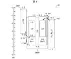
- 4 is a diagram illustrating the band levels of a hole transport layer, a red light emitting layer, and an electron transport layer provided in a red light emitting element of the display device of the present embodiment.
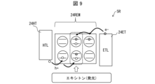
- FIG. 1 is a diagram for explaining the reason why good external quantum efficiency (EQE) can be realized in the red light emitting element of the display device of the present embodiment.
- FIG. 13 is a diagram illustrating the band levels of a hole transport layer, a red light-emitting layer, and an electron transport layer provided in a red light-emitting element as a comparative example.
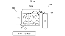
- FIG. 1 is a diagram for explaining the reason why a good external quantum efficiency (EQE) cannot be realized in a red light-emitting element as a comparative example.
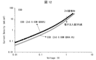
- This figure shows the relationship between voltage and current density for an Electron Only Device (EOD) including a red light-emitting layer formed using a quantum dot solution with a concentration of 0.02 M, out of the multiple types of quantum dot solutions shown in Figure 7, and an Electron Only Device (EOD) including a red light-emitting layer formed using a quantum dot solution with a concentration of 0.08 M.
- EOD Electron Only Device
- EOD Electron Only Device
- FIG. 11 is a diagram showing the degree of luminance decrease due to charge-up of quantum dots when a red light-emitting element including a red light-emitting layer formed using a quantum dot solution having a concentration of 0.01 M among the multiple types of quantum dot solutions shown in FIG. 7 and a red light-emitting element as a comparative example shown in FIG.
- This figure shows the PL intensity (photoluminescence intensity) at each wavelength for a red light-emitting layer formed using a quantum dot solution with a concentration of 0.01 M from the multiple types of quantum dot solutions shown in Figure 7, and a red light-emitting layer formed using a quantum dot solution with a concentration of 0.16 M as a comparison example.
- This figure shows the relationship between the weight ratio of a continuous film containing metal sulfides, which is a medium in multiple types of red light-emitting layers, which are thin films formed using multiple types of quantum dot solutions as shown in Figure 7, and the internal quantum yield (PLQY).
- FIG. 8 is a diagram showing the emission peak wavelength, the internal quantum yield (PLQY), the maximum external quantum efficiency (maximum EQE), and the luminance reduction rate after 5 hours of operation for multiple types of red light-emitting elements including a red light-emitting layer formed using multiple types of quantum dot solutions shown in FIG.
- FIG. 8 is a diagram showing the degree of change in luminance and voltage over the driving time of a red light-emitting element including a red light-emitting layer formed using a quantum dot solution having a concentration of 0.04 M among the multiple types of quantum dot solutions shown in FIG. FIG.
- FIG. 8 is a diagram showing the degree of change in luminance and voltage over the driving time of a red light-emitting element including a red light-emitting layer formed using a quantum dot solution having a concentration of 0.08 M among the multiple types of quantum dot solutions shown in FIG. 5A to 5C are diagrams for explaining a step of forming a red light-emitting layer included in the manufacturing method of a red light-emitting element provided in the display device of the present embodiment.
- FIG. 1 is a plan view showing the schematic configuration of the display device 1 of this embodiment.
- the display device 1 has a frame area NDA and a display area DA.
- the display area DA of the display device 1 has a plurality of pixels PIX, each of which includes a red subpixel RSP, a green subpixel GSP, and a blue subpixel BSP.
- a case in which one pixel PIX is composed of a red subpixel RSP, a green subpixel GSP, and a blue subpixel BSP will be described as an example, but this is not limiting.
- one pixel PIX may include subpixels of other colors in addition to the red subpixel RSP, green subpixel GSP, and blue subpixel BSP.
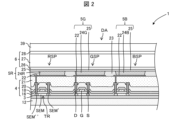
- FIG. 2 is a cross-sectional view showing the schematic configuration of the display area DA of the display device 1 of this embodiment.
- a barrier layer 3 As shown in FIG. 2, in the display area DA of the display device 1, a barrier layer 3, a thin-film transistor layer 4 including a transistor TR, a red light-emitting element 5R, a green light-emitting element 5G, a blue light-emitting element 5B, a bank 23, a sealing layer 6, and a functional film 39 are provided on a substrate 12 in this order from the substrate 12 side.
- the red sub-pixel RSP provided in the display area DA of the display device 1 includes a red light-emitting element 5R
- the green sub-pixel GSP provided in the display area DA of the display device 1 includes a green light-emitting element 5G
- the blue sub-pixel BSP provided in the display area DA of the display device 1 includes a blue light-emitting element 5B.
- the substrate 12 may be, for example, a resin substrate made of a resin material such as polyimide, or a glass substrate.
- a resin substrate made of a resin material such as polyimide is used as the substrate 12 in order to make the display device 1 a flexible display device, a case where a resin substrate made of a resin material such as polyimide is used as the substrate 12 will be described as an example, but this is not limited to this. If the display device 1 is a non-flexible display device, a glass substrate can be used as the substrate 12.
- the barrier layer 3 is a layer that prevents foreign substances such as water and oxygen from penetrating the transistor TR, the red light-emitting element 5R, the green light-emitting element 5G, and the blue light-emitting element 5B, and can be composed of, for example, a silicon oxide film, a silicon nitride film, or a silicon oxynitride film, or a laminate film of these, formed by the CVD method.
- the transistor TR portion of the thin-film transistor layer 4 including the transistor TR includes the semiconductor film SEM and doped semiconductor films SEM' and SEM'', the inorganic insulating film 16, the gate electrode G, the inorganic insulating film 18, the inorganic insulating film 20, the source electrode S and the drain electrode D, and the planarization film 21, and the portion of the thin-film transistor layer 4 including the transistor TR other than the transistor TR portion includes the inorganic insulating film 16, the inorganic insulating film 18, the inorganic insulating film 20, and the planarization film 21.
- the semiconductor films SEM, SEM', and SEM'' may be made of, for example, low-temperature polysilicon (LTPS) or an oxide semiconductor (for example, an In-Ga-Zn-O-based semiconductor).
- LTPS low-temperature polysilicon
- oxide semiconductor for example, an In-Ga-Zn-O-based semiconductor.
- the gate electrode G and the source and drain electrodes S and D can be formed of a single layer or a multilayer film of a metal containing at least one of aluminum, tungsten, molybdenum, tantalum, chromium, titanium, and copper, for example.
- Inorganic insulating film 16, inorganic insulating film 18, and inorganic insulating film 20 can be composed of, for example, a silicon oxide film, a silicon nitride film, a silicon oxynitride film, or a laminate film of these films formed by the CVD method.
- the planarization film 21 can be made of a coatable organic material such as polyimide or acrylic, but it may also be made of an inorganic film.
- the red light-emitting element 5R included in the red subpixel RSP includes an anode 22 above the planarization film 21, a functional layer 24R including a red light-emitting layer, and a cathode 25.
- the green light-emitting element 5G included in the green subpixel GSP includes an anode 22 above the planarization film 21, a functional layer 24G including a green light-emitting layer, and a cathode 25.
- the blue light-emitting element 5B included in the blue subpixel BSP includes an anode 22 above the planarization film 21, a functional layer 24B including a blue light-emitting layer, and a cathode 25.
- the insulating bank 23 covering the edge of the anode 22 can be formed by applying an organic material such as polyimide or acrylic and then patterning it by photolithography, but it may also be formed from an inorganic film.
- the red light emitting element 5R, the green light emitting element 5G, and the blue light emitting element 5B have a forward stack structure is described as an example, but this is not limited thereto, and the red light emitting element 5R, the green light emitting element 5G, and the blue light emitting element 5B may have an inverted stack structure.
- the red light emitting element 5R having a forward stack structure has an anode 22 and a cathode 25 provided as an upper layer above the anode 22, and the functional layer 24R including a red light emitting layer provided between the anode 22 and the cathode 25 can be formed, for example, by stacking a hole injection layer, a hole transport layer, a red light emitting layer, an electron transport layer, and an electron injection layer in this order from the anode 22 side.
- the functional layer 24R including a red light emitting layer one or more layers of the hole injection layer, hole transport layer, electron transport layer, and electron injection layer other than the red light emitting layer may be omitted as appropriate.
- the functional layer 24R including the red light-emitting layer 24REM is constructed by stacking, in order from the anode 22 side, a hole transport layer 24HT, a red light-emitting layer 24REM, and an electron transport layer 24ET, but the present invention is not limited to this.
- the red light emitting element having an inverted stack structure has a cathode and an anode provided as an upper layer than the cathode, and the functional layer including the red light emitting layer 24REM provided between the cathode and the anode can be constructed by stacking, for example, an electron injection layer, an electron transport layer, the red light emitting layer 24REM, a hole transport layer, and a hole injection layer in this order from the cathode side.
- the functional layers including the red light emitting layer 24REM one or more layers of the electron injection layer, electron transport layer, hole transport layer, and hole injection layer other than the red light emitting layer 24REM may be omitted as appropriate.
- the material used for the hole injection layer is not particularly limited as long as it is a hole injection material that can stabilize the injection of holes into the light-emitting layer.
- a composite of poly(3,4-ethylenedioxythiophene) (PEDOT) and polystyrene sulfonic acid (PSS) (PEDOT:PSS) can be used.
- Materials used for the hole transport layer may be, for example, organic materials such as poly[(9,9-dioctylfluorenyl-2,7-diyl)-co-(4,4'-(N-(4-sec-butylphenyl))diphenylamine)] (TFB), N,N'-bis(4-butylphenyl)-N,N'-bis(phenyl)-benzidine (poly-TPD) or polyvinylcarbazole (PVK), or nanoparticles having hole transport properties such as NiO particles.
- organic materials such as poly[(9,9-dioctylfluorenyl-2,7-diyl)-co-(4,4'-(N-(4-sec-butylphenyl))diphenylamine)] (TFB), N,N'-bis(4-butylphenyl)-N,N'-bis(phenyl)-benzidine (poly-TPD)
- N,N'-bis(4-butylphenyl)-N,N'-bis(phenyl)-benzidine (poly-TPD) is used as the hole transport layer 24HT will be described as an example, but the present invention is not limited to this.
- the material used for the electron transport layer may be, for example, an organic material such as 2,2',2"-(1,3,5-benzinetriyl)-tris(1-phenyl-1-H-benzimidazole) (TPBi), or nanoparticles having electron transport properties such as ZnO particles.
- TPBi 2,2',2"-(1,3,5-benzinetriyl)-tris(1-phenyl-1-H-benzimidazole)
- nanoparticles having electron transport properties such as ZnO particles.
- the electron transport layer 24ET is described using, as an example, particles of an oxide containing Zn and Mg, for example, Zn0.9Mg0.1O particles, but is not limited to this.
- the material used for the electron injection layer is not particularly limited as long as it is an electron injection material that can stabilize the injection of electrons into the light-emitting layer.
- alkali metals or alkaline earth metals such as aluminum, strontium, calcium, lithium, cesium, magnesium oxide, aluminum oxide, strontium oxide, lithium oxide, lithium fluoride, magnesium fluoride, strontium fluoride, calcium fluoride, barium fluoride, cesium fluoride, polymethyl methacrylate polystyrene sodium sulfonate, oxides of alkali metals or alkaline earth metals, fluorides of alkali metals or alkaline earth metals, organic complexes of alkali metals, etc. can be used.
- the functional layer 24R including the red light-emitting layer, the functional layer 24G including the green light-emitting layer, and the functional layer 24B including the blue light-emitting layer each have a hole transport layer formed in the same process using the same material, and an electron transport layer formed in the same process using the same material, but this is not limited to this.
- the hole injection layers included in each of the functional layers 24R, 24G, and 24B may be formed in the same process using the same material, or may be formed from different materials, and the hole injection layers included in two of the functional layers 24R, 24G, and 24B may be formed in the same process using the same material, and only the hole injection layer included in the remaining functional layer may be formed in a different process using a different material.
- the hole transport layers included in each of the functional layers 24R, 24G, and 24B may be formed from different materials, or the hole transport layers included in two of the functional layers 24R, 24G, and 24B may be formed in the same process using the same material, and only the hole transport layer included in the remaining functional layer may be formed in a different process using a different material.
- the same materials and the same process can be appropriately selected for the electron transport layers in the functional layers 24R, 24G, and 24B in the desired combination.
- the red light-emitting element 5R, the green light-emitting element 5G, and the blue light-emitting element 5B are all QLEDs (quantum dot light-emitting diodes) will be described as an example, but this is not limited thereto, and it is sufficient that one or more of the red light-emitting element 5R, the green light-emitting element 5G, and the blue light-emitting element 5B are QLEDs, and the rest may be OLEDs.
- the light emitting layer of each light emitting element contains quantum dots.
- the quantum dots may have, for example, a core structure, a core/shell structure, a core/shell/shell structure, or a shell structure in which the core/ratio is continuously changed.
- the shell may cover a part of the core, but it is more preferable that the shell completely covers the core.
- Examples of the core material of the quantum dot include crystals of II-VI group semiconductors such as MgS, MgSe, MgTe, CaS, CaSe, CaTe, BaS, BaSe, BaTe, ZnS, ZnSe, ZnTe, CdS, CdSe, CdTe, PbS, PbSe, HgS, HgSe, and HgTe, crystals of III-V group semiconductors such as GaAs, GaP, InN, InAs, InP, and InSb, and crystals of Ga 3 S 2 , Ga 2 Se 3 , In 2 S 3 , and In 2 Se.
- II-VI group semiconductors such as MgS, MgSe, MgTe, CaS, CaSe, CaTe, BaS, BaSe, BaTe, ZnS, ZnSe, ZnTe, CdS, CdSe, CdTe, PbS, PbSe, H
- the shell material can be composed of a crystal of a III-VI group semiconductor such as CuInGaS, AgInGaS, CuInGaS, AgInGaZnS, CuInGaSe, AgInGaSe, etc., a crystal of a I-III-VI group semiconductor such as CuInGaS, AgInGaS, CuInGaS, AgInGaZnS, CuInGaSe, AgInGaSe, etc., a crystal of a group IV semiconductor such as C or Si, etc., or a crystal of a semiconductor with a perovskite structure such as CsPbI 3 , CsPbBr 3 , CsPbCl 3, etc.
- the shell material is selected from the same material group as the core material, and is preferably one that has a lattice constant close to that of the core material and a larger band gap than the core material.
- the quantum dot means one that includes an organic or inorganic ligand.
- the quantum dots include a ligand such as an organic or inorganic ligand
- each of the red light-emitting layer 24REM, the green light-emitting layer, and the blue light-emitting layer also includes a ligand.
- the maximum width of the quantum dot excluding the ligand portion is 100 nm or less.
- the shape of the quantum dot excluding the ligand portion may be any shape that satisfies the above maximum width, and is not particularly restricted, and is not limited to a spherical three-dimensional shape (circular cross-sectional shape). For example, it may be a polygonal cross-sectional shape, a rod-shaped three-dimensional shape, a branch-shaped three-dimensional shape, a three-dimensional shape with unevenness on the surface, or a combination of these.
- the red light emitting element 5R, green light emitting element 5G, and blue light emitting element 5B have a forward stack structure in which the cathode 25 is disposed above the anode 22.
- the anode 22 may be formed from an electrode material that reflects visible light
- the cathode 25 may be formed from an electrode material that transmits visible light.
- the anode 22 may be formed from an electrode material that transmits visible light
- the cathode 25 may be formed from an electrode material that reflects visible light.
- the cathode 25 should be formed from an electrode material that reflects visible light, and the anode 22 should be formed from an electrode material that transmits visible light; in order to achieve a bottom emission type, the cathode 25 should be formed from an electrode material that transmits visible light, and the anode 22 should be formed from an electrode material that reflects visible light.
- the electrode material that reflects visible light is not particularly limited as long as it can reflect visible light and has electrical conductivity, but examples include metal materials such as Al, Mg, Li, and Ag, alloys of the above metal materials, laminates of the above metal materials and transparent metal oxides (e.g., indium tin oxide, indium zinc oxide, indium gallium zinc oxide, etc.), and laminates of the above alloys and the above transparent metal oxides.
- metal materials such as Al, Mg, Li, and Ag
- alloys of the above metal materials such as Al, Mg, Li, and Ag
- alloys of the above metal materials such as Al, Mg, Li, and Ag
- laminates of the above metal materials and transparent metal oxides e.g., indium tin oxide, indium zinc oxide, indium gallium zinc oxide, etc.
- laminates of the above alloys and the above transparent metal oxides e.g., indium tin oxide, indium zinc oxide, indium gallium zinc oxide, etc.
- electrode materials that transmit visible light are not particularly limited as long as they are capable of transmitting visible light and have electrical conductivity, but examples include transparent metal oxides (e.g., indium tin oxide, indium zinc oxide, indium gallium zinc oxide, etc.), thin films made of metal materials such as Al and Ag, and nanowires made of metal materials such as Al and Ag.
- transparent metal oxides e.g., indium tin oxide, indium zinc oxide, indium gallium zinc oxide, etc.
- thin films made of metal materials such as Al and Ag
- nanowires made of metal materials such as Al and Ag.
- the anode 22 and the cathode 25 can be formed by a method that is generally used for forming electrodes, such as physical vapor deposition (PVD) methods such as vacuum deposition, sputtering, EB deposition, and ion plating, or chemical vapor deposition (CVD).
- PVD physical vapor deposition
- CVD chemical vapor deposition
- the method for patterning the anode 22 and the cathode 25 is not particularly limited as long as it can be formed into the desired pattern with high precision, but specific examples include photolithography and inkjet methods.
- the sealing layer 6 is a light-transmitting film, and can be composed of, for example, an inorganic sealing film 26 that covers the cathode 25, an organic film 27 that is above the inorganic sealing film 26, and an inorganic sealing film 28 that is above the organic film 27.
- the sealing layer 6 prevents foreign matter such as water and oxygen from penetrating into the red light-emitting element 5R, the green light-emitting element 5G, and the blue light-emitting element 5B.
- the inorganic sealing film 26 and the inorganic sealing film 28 are inorganic films, and may be formed, for example, by a CVD method, such as a silicon oxide film, a silicon nitride film, or a silicon oxynitride film, or a laminated film of these.
- the organic film 27 is a light-transmitting organic film with a planarizing effect, and may be formed, for example, by a coatable organic material such as acrylic.
- the organic film 27 may be formed, for example, by an inkjet method.
- the sealing layer 6 is formed of two inorganic films and one organic film provided between the two inorganic films, but the stacking order of the two inorganic films and one organic film is not limited to this.
- the sealing layer 6 may be formed only of an inorganic film, may be formed only of an organic film, may be formed of one inorganic film and two organic films, or may be formed of two or more inorganic films and two or more organic films.
- the functional film 39 is, for example, a film having at least one of an optical compensation function, a touch sensor function, and a protective function.
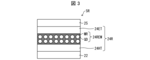
- FIG. 3 is a cross-sectional view showing the schematic configuration of the red light-emitting element 5R provided in the display device 1 of this embodiment.
- the red light-emitting element 5R includes an anode 22, a cathode 25, and a red light-emitting layer 24REM disposed between the anode 22 and the cathode 25.
- the functional layer 24B including the red light-emitting layer 24REM of the red light-emitting element 5R is configured by stacking a hole transport layer 24HT, a red light-emitting layer 24REM, and an electron transport layer 24ET in this order from the anode 22 side.
- the red light-emitting layer 24REM includes a continuous film MR containing a metal sulfide, and a plurality of quantum dots QDs encapsulated in the continuous film MR.
- a case in which all of the quantum dots QDs in the red light-emitting layer 24REM are encapsulated in the continuous film MR will be described as an example, but this is not limited to the case as long as the red light-emitting layer 24REM includes a plurality of quantum dots QDs encapsulated in the continuous film MR.
- the continuous film MR may be a matrix.
- the continuous film MR is a continuous matrix.
- the matrix means a material that contains and holds other things, and can be rephrased as a base material, a base material, or a filler.
- the continuous matrix may be a material that contains and holds multiple quantum dots QDs.
- the matrix may be filled in the light-emitting layer.
- the matrix may fill the area (space) between two adjacent quantum dots QDs.
- the matrix may fill areas (spaces) in the light-emitting layer other than the multiple quantum dots QDs.
- the matrix being filled between multiple quantum dots QDs means that the area between two adjacent quantum dots QDs is filled with the matrix, and it is sufficient to know that.
- the outer edge (upper and lower surfaces) of the light-emitting layer may be covered with the matrix.
- the light-emitting layer may be configured to have a matrix portion from the outer edge, and the quantum dot group may be located away from the outer edge.
- the outer edge of the light-emitting layer may not be formed only of the matrix, and a part of the quantum dot group may be exposed from the matrix.
- the matrix may refer to a portion of the light-emitting layer other than the quantum dot group.
- the matrix may be formed so as to partially or completely fill a space formed between two adjacent quantum dots QDs.
- the light-emitting layer may have a gap.
- the light-emitting layer may have a plurality of quantum dots QDs contained in a matrix, and the matrix may partially or completely fill an area other than the plurality of quantum dots QDs.
- Each of the two adjacent quantum dots QDs included in the plurality of quantum dots QDs may be embedded in the matrix at an interval.
- the continuous matrix may be made of the same material as the shell of the quantum dot QD.
- the average distance (core distance) between adjacent cores of two adjacent quantum dot QDs may be 3 nm or more, and may be 5 nm or more.
- the core distance is the average distance between 20 adjacent cores in a space containing 20 cores.
- the core distance should be kept wider than the distance when the shells are in contact with each other.
- the size of the cross section varies depending on the cutting position of the particle. For this reason, the diameter of a circle having the same area as the average cross section of the top 10% of particles with the largest cross sections can be regarded as the core diameter.
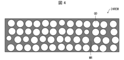
- FIG. 4 is a cross-sectional view showing the schematic configuration of the red light-emitting layer 24REM of the red light-emitting element 5R provided in the display device 1 of this embodiment.
- the area C of the cross section of the portion of the red light-emitting layer 24REM is smaller than twice the area B of the combined cross section areas of the predetermined number of quantum dots QDs.
- the area A is smaller than the area B.
- the area of the cross section of the portion of the red light-emitting layer 24REM including the cross section of the 52 quantum dots QDs is area C, that is, if the area of the cross section of the portion of the entire light-emitting layer including the cross section of the quantum dots QDs and the matrix is area C, the area C is smaller than twice the area B of the total cross section of the 52 quantum dots QDs.
- the case of a cross section of a portion of the red light-emitting layer 24REM including 52 quantum dots QDs has been described as an example, but is not limited to this. It is sufficient that there are 50 or more quantum dots QDs, and it may be 50 or 100 quantum dots QDs.
- the cross-sectional size of the 52 quantum dots QD varies depending on the cutting position even if the quantum dots QD have the same particle diameter. Also, for example, when the cross-section of the red light-emitting layer 24REM is observed with a transmission electron microscope (TEM), if it contains voids of a size that can be identified, the cross-sectional area of these voids is not included in the cross-sectional area A of the continuous film MR containing metal sulfide.
- TEM transmission electron microscope
- the red light-emitting layer 24REM is described as an example in which the cross-sectional area A of the continuous film MR containing metal sulfide is smaller than the combined area B of the cross-sectional areas of a predetermined number, for example, 50 or more quantum dots QDs, in any cross-section obtained by cutting any part of the red light-emitting layer 24REM.
- the red light-emitting layer 24REM may include a cross-section including the predetermined number, for example, 50 or more quantum dots QDs, obtained by cutting a certain part of the red light-emitting layer 24REM, in which the cross-sectional area A of the continuous film MR containing metal sulfide is smaller than the combined area B of the cross-sectional areas of the predetermined number, for example, 50 or more quantum dots QDs.
- the fact that the red light emitting layer 24REM has a cross section in a portion where the cross section area A of the continuous film MR containing metal sulfide is smaller than the area B obtained by adding up the cross sections of a predetermined number, for example, 50 or more quantum dots QD means that the red light emitting layer 24REM includes a portion where the cross section area A of the continuous film MR containing metal sulfide is smaller than the area B obtained by adding up the cross sections of a predetermined number, for example, 50 or more quantum dots QD.
- the inventors of the present disclosure have confirmed that if the red light emitting layer 24REM includes a cross section including a predetermined number, for example, 50 or more quantum dots QDs, where the cross section area A of the continuous film MR containing metal sulfide is smaller than the area B obtained by adding up the cross sections of the predetermined number, for example, 50 or more quantum dots QDs, the carrier balance and external quantum efficiency (EQE) can be improved and the decrease in luminance due to charge-up of the quantum dots can be suppressed.
- EQE carrier balance and external quantum efficiency
- the red light-emitting layer 24REM may include a cross section including a predetermined number of quantum dots QDs, for example, 50 quantum dots QDs, where the area A of the cross section of the continuous film MR containing metal sulfide is smaller than the area B of the total cross sections of the quantum dots QDs, for example, 50 quantum dots QDs, or may include a cross section including 100 quantum dots QDs, where the area A of the cross section of the continuous film MR containing metal sulfide is smaller than the area B of the total cross sections of the 100 quantum dots QDs.
- the area of the cross section of a portion of the red light-emitting layer 24REM including 52 quantum dots QDs may be, for example, an area obtained by observing a cross section of a portion of the red light-emitting layer 24REM including 52 quantum dots QDs shown in FIG. 4 with a transmission electron microscope (TEM) and excluding voids that can be identified by the transmission electron microscope (TEM) from the value of the width in the horizontal direction of the cross section of the portion of the red light-emitting layer 24REM shown in FIG. 4 times the height in the vertical direction of the cross section of the portion of the red light-emitting layer 24REM shown in FIG. 4.
- TEM transmission electron microscope
- the cross-sectional area A of the continuous film MR that includes metal sulfide is preferably 3.4% or more and 27.0% or less of the area B that is the sum of the cross-sectional areas of the predetermined number, for example, 50 or more quantum dots QDs.
- a cross section of a portion of the red light-emitting layer 24REM including a cross section of a predetermined number of quantum dots QDs shown in FIG. 4, for example, 50 or more, may be observed with a transmission electron microscope (TEM).
- the image of the transmission electron microscope (TEM) may include a first region having a higher electron density through which the irradiated electron beam has passed, and a second region having a lower electron density, and the area of the first region may be area A of the cross section of the continuous film MR including metal sulfide calculated from area C minus area B, and the area of the second region may be area B, which is the sum of the cross-sectional areas of the 52 quantum dots QDs.
- TEM transmission electron microscope
- Quantum dots QD such as ZnSe, InP, and CdS
- Se, In, and Cd which are heavier elements than Zn, and are therefore displayed in a lighter color
- the area B which is the area of the second region with lower electron density
- continuous film MR containing metal sulfide e.g., ZnS
- ZnS contains Zn, which is a lighter element than Se, and is therefore displayed in a darker color
- the area A which is the area of the first region with higher electron density
- X-ray diffraction may be performed on a cross-section of a portion of the red light-emitting layer 24REM containing cross-sections of a predetermined number of quantum dots QDs, for example, 50 or more, as shown in Figure 4.
- a cross section of a portion of the red light-emitting layer 24REM containing cross sections of 50 or more quantum dots QDs includes a first region having a specific diffraction peak due to X-ray diffraction of metal sulfide and a second region having a specific diffraction peak due to X-ray diffraction of quantum dots QDs, and the area of the first region in the cross section of the portion of the red light-emitting layer 24REM calculated based on the specific diffraction peak due to X-ray diffraction of metal sulfide may be area A of the cross section of the continuous film MR containing metal sulfide calculated from area C - area B, and the area of the second region in the cross section of the portion of the red light-emitting layer 24REM calculated based on the specific diffraction peak due to X-ray diffraction of quantum dots QDs may be area B, which is the sum of the areas of the cross sections of the 50 or more quantum dots QD
- the number-average inter-quantum dot distance of the 50 or more quantum dots QDs is preferably 1 nm or more and 5 nm or less.
- the number-average inter-quantum dot distance is a value that can be calculated by calculating the distance between adjacent quantum dots QDs that have the shortest inter-quantum dot distance N times (N is a natural number of 2 or more) in a cross section of a portion of the red light-emitting layer 24REM including 50 or more quantum dots QDs as shown in FIG. 4, and calculating the sum of the shortest distances of the N times/N.
- FIG. 5 shows the red light-emitting layer 24REM of the red light-emitting element 5R provided in the display device 1 of this embodiment, in which the material of the shell SH of the quantum dot QD contained in the red light-emitting layer 24REM and the continuous film MR containing metal sulfide are made of the same material.
- the quantum dot QD contained in the red light-emitting layer 24REM includes a core CO and a shell SH, and the shell SH of the quantum dot QD is composed of a metal sulfide.
- the metal sulfide contained in the continuous film MR and the metal sulfide constituting the shell SH of the quantum dot QD are both ZnS will be described as an example, but is not limited to this.
- the metal sulfide contained in the continuous film MR and the metal sulfide constituting the shell SH of the quantum dot QD may be different metal sulfides.
- the metal sulfide may contain one or more metal elements selected from Zn, Mg, and Ga, and may be any of zinc sulfide (e.g., ZnS), zinc magnesium sulfide (e.g., ZnMgS), gallium sulfide (e.g., GaS), zinc selenide sulfide (e.g., ZnSeS), zinc telluride sulfide (e.g., ZnTeS), magnesium sulfide (e.g., MgS), and zinc gallium sulfide (e.g., ZnGaS).
- the band gap of the continuous film MR which contains the metal sulfide matrix, is larger than the band gap of the core CO of the quantum dot QD.
- the shell SH of the quantum dot QD is composed of a metal sulfide
- the metal sulfide contained in the continuous film MR and the metal sulfide that composes the shell SH of the quantum dot QD are both ZnS
- the shell SH of the quantum dot QD that is composed of a metal sulfide is formed continuously with the continuous film MR, and can therefore be regarded as the continuous film MR.
- FIG. 6 shows another red light-emitting layer 24REM' that can be provided in the red light-emitting element 5R provided in the display device 1 of this embodiment, in which the material of the shell SH' of the quantum dot QD' contained in the red light-emitting layer 24REM' is different from the material of the continuous film MR containing metal sulfide.
- the quantum dot QD' contained in the red light-emitting layer 24REM' includes a core CO and a shell SH', and the shell SH' of the quantum dot QD' is composed of a material other than metal sulfide, and the band gap of the continuous film MR containing metal sulfide, which is the matrix, is larger than the band gap of the core CO of the quantum dot QD'.
- the shell SH' of the quantum dot QD' is composed of something other than metal sulfide, the shell SH' of the quantum dot QD' does not contain metal sulfide, and so it is a quantum dot QD.
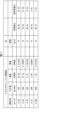
- FIG. 7 shows an example of multiple types of quantum dot solutions that contain multiple quantum dots QD, a metal sulfide precursor, and a solvent and can be used in the process of forming the red light-emitting layer 24REM of the red light-emitting element 5R provided in the display device 1 of this embodiment.
- the case where zinc ethylxanthate, which decomposes after heat treatment to form ZnS, is used as the precursor of the metal sulfide is described as an example, but is not limited to this.
- a metal complex in which one or more selected from thiourea, N-methylthiourea, 1,3-dimethylthiourea, N,N'-dimethylthiourea, tetramethylthiourea, thioacetamide, and xanthogenic acid are coordinated to a metal atom may be used.
- the precursor of the metal sulfide is composed of a metal source and a sulfur source
- the metal source is one or more selected from metal acetates, metal nitrates, and metal halide salts
- the sulfur source may be one or more selected from thiourea, N-methylthiourea, 1,3-dimethylthiourea, N,N'-dimethylthiourea, tetramethylthiourea, and thioacetamide.
- a quantum dot QD in which the core is made of InP, the shell is made of ZnS, and the ligand contains a halogen ligand, but this is not limiting.
- N,N-dimethylformamide as a solvent is described as an example, but the present invention is not limited to this, and for example, dimethyl sulfoxide may also be used.
- the quantum dot solution shown in Figure 7 with a concentration [M] of 0.08 is a solution in which quantum dots QDs, zinc ethylxanthate, and N,N-dimethylformamide are mixed so that the concentration of quantum dots QDs is 15 mg/ml and the concentration of zinc ethylxanthate, the precursor of metal sulfide, is 24.64 mg/ml.
- the weight ratio of quantum dots QDs in the red light-emitting layer 24REM formed using the quantum dot solution with a concentration [M] of 0.08 is 64.6%, and the weight ratio of the continuous film MR (medium) is 35.4%.
- the quantum dot solution shown in Figure 7 with a concentration [M] of 0.04 is a solution in which quantum dots QDs, zinc ethylxanthate, and N,N-dimethylformamide are mixed so that the concentration of quantum dots QDs is 15 mg/ml and the concentration of zinc ethylxanthate, the precursor of metal sulfide, is 12.32 mg/ml.
- the weight ratio of quantum dots QDs in the red light-emitting layer 24REM formed using the quantum dot solution with a concentration [M] of 0.04 is 78.5%, and the weight ratio of the continuous film MR (medium) is 21.5%.
- the quantum dot solution shown in Figure 7 with a concentration [M] of 0.02 is a solution in which quantum dots QDs, zinc ethylxanthate, and N,N-dimethylformamide are mixed so that the concentration of quantum dots QDs is 15 mg/ml and the concentration of zinc ethylxanthate, the precursor of metal sulfide, is 6.16 mg/ml.
- the weight ratio of quantum dots QDs in the red light-emitting layer 24REM formed using the quantum dot solution with a concentration [M] of 0.02 is 88.0%, and the weight ratio of the continuous film MR (medium) is 12.0%.
- the quantum dot solution shown in Figure 7 with a concentration [M] of 0.01 is a solution in which quantum dots QDs, zinc ethylxanthate, and N,N-dimethylformamide are mixed so that the concentration of quantum dots QDs is 15 mg/ml and the concentration of zinc ethylxanthate, the precursor of metal sulfide, is 3.08 mg/ml.
- the weight ratio of quantum dots QDs in the red light-emitting layer 24REM formed using the quantum dot solution with a concentration [M] of 0.01 is 93.6%, and the weight ratio of the continuous film MR (medium) is 6.4%.
- the quantum dot solution shown in Figure 7 with a concentration [M] of 0.005 is a solution in which quantum dots QDs, zinc ethylxanthate, and N,N-dimethylformamide are mixed so that the concentration of quantum dots QDs is 15 mg/ml and the concentration of zinc ethylxanthate, the precursor of metal sulfide, is 1.54 mg/ml.
- the weight ratio of quantum dots QDs in the red light-emitting layer 24REM formed using the quantum dot solution with a concentration [M] of 0.005 is 96.7%, and the weight ratio of the continuous film MR (medium) is 3.3%.
- the red light-emitting layer 24REM is formed using any of the quantum dot solutions with a concentration [M] of 0.08, 0.04, 0.02, 0.01, or 0.005 shown in FIG. 7 described above, in a cross section of a portion of the red light-emitting layer 24REM that includes cross sections of 50 or more quantum dots QDs among the multiple quantum dots QDs contained in the red light-emitting layer 24REM, the cross-sectional area A of the continuous film MR containing metal sulfide is smaller than the combined area B of the cross-sectional areas of the 50 or more quantum dots QDs.
- FIG. 8 is a diagram showing the band levels of the hole transport layer 24HT, the red light-emitting layer 24REM, and the electron transport layer 24ET provided in the red light-emitting element 5R of the display device 1 of this embodiment.
- the cross-sectional area A of the continuous film MR including metal sulfide is smaller than the combined area B of the cross-sectional areas of the 50 or more quantum dots QDs.
- holes H are injected from the upper valence band level (-5.3 eV) of the hole transport layer 24HT to the upper valence band level (-5.6 eV) of the quantum dot QD core CO and the upper valence band level (-6.8 eV) of the quantum dot QD shell SH, and electrons E are injected from the lower conduction band level (-3.5 eV) of the electron transport layer 24ET to the lower conduction band level (-3.6 eV) of the quantum dot QD core CO and the lower conduction band level (-3.1 eV to -3.3 eV) of the quantum dot QD shell SH, ensuring a good carrier balance between holes H and electrons E.
- FIG. 9 is a diagram explaining why good external quantum efficiency (EQE) can be achieved in the red light-emitting element 5R of the display device 1 of this embodiment.
- the red light-emitting element 5R As described above, in the case of the red light-emitting element 5R, a good carrier balance between the holes H and the electrons E can be ensured, and as shown in FIG. 9, the holes H and the electrons E recombine in the center of the red light-emitting layer 24REM and emit light as excitons, thereby achieving good external quantum efficiency (EQE).
- the red light-emitting element 5R can improve durability and luminous efficiency.
- FIG. 10 is a diagram showing the band levels of the hole transport layer 24HT, the red light-emitting layer 74REM, and the electron transport layer 24ET in the red light-emitting element 50R, which is a comparative example.
- the red light-emitting layer 74REM provided in the red light-emitting element 50R which is a comparative example, is a layer formed using a quantum dot solution with a concentration [M] of 0.3, for example.
- the quantum dot solution with a concentration [M] of 0.3 is a solution in which quantum dots QDs, zinc ethylxanthate, and N,N-dimethylformamide are mixed so that the concentration of the quantum dots QDs is 15 mg/ml and the concentration of zinc ethylxanthate, which is a precursor of metal sulfide, is 92.4 mg/ml.
- the weight ratio of the quantum dots QDs is 32.7%, and the weight ratio of the continuous film MR (medium) is 67.3%.
- the cross-sectional area A of the continuous film MR that includes metal sulfide is greater than the combined area B of the cross-sectional areas of the 50 or more quantum dots QDs.
- the cross-sectional area A of the continuous film MR including metal sulfide is larger than the combined area B of the cross-sectional areas of the 50 or more quantum dots QDs.
- holes H are mainly injected from the upper valence band level of the hole transport layer 24HT (-5.3 eV) to the upper valence band level of the shell SH of the quantum dot QD (-6.8 eV), which has a relatively large level difference of 1.5 eV, and are less likely to be injected into the upper valence band level of the core CO of the quantum dot QD (-5.6 eV), which has a relatively small level difference of 0.3 eV, due to the influence of the continuous film MR containing metal sulfide, which occupies a large portion of the red light-emitting layer 74REM.
- electrons E are injected from the conduction band lower edge level (-3.5 eV) of the electron transport layer 24ET to the conduction band lower edge level (-3.6 eV) of the quantum dot QD core CO and to the conduction band lower edge level (-3.1 eV to -3.3 eV) of the quantum dot QD shell SH, so that the red light-emitting layer 74REM is in an excess state of electrons E, and the carrier balance between holes H and electrons E is disrupted.
- FIG. 11 is a diagram explaining why good external quantum efficiency (EQE) cannot be achieved in the red light-emitting element 50R, which is a comparative example.
- Figure 12 shows the relationship between voltage and current density for an electron only device (EOD) including a red light emitting layer 24REM formed using a quantum dot solution with a concentration of 0.02 M out of the multiple types of quantum dot solutions shown in Figure 7, and an electron only device (EOD) including a red light emitting layer 24REM formed using a quantum dot solution with a concentration of 0.08 M.
- EOD electron only device
- EOD electron only device
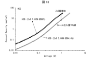
- Figure 13 shows the relationship between voltage and current density for a Hole Only Device (HOD) including a red light-emitting layer 24REM formed using a quantum dot solution with a concentration of 0.02 M out of the multiple types of quantum dot solutions shown in Figure 7, and a Hole Only Device (HOD) including a red light-emitting layer 24REM formed using a quantum dot solution with a concentration of 0.08 M.
- HOD Hole Only Device
- HOD Hole Only Device
- FIG. 17 shows the emission peak wavelength, internal quantum yield (PLQY), maximum external quantum efficiency (maximum EQE), and luminance reduction rate after 5 hours of operation for multiple types of red light-emitting elements 5R including red light-emitting layers 24REM formed using multiple types of quantum dot solutions shown in FIG. 7.
- red light-emitting layer 24REM using a quantum dot solution with a concentration [M] of 0.08, 0.04, 0.02, or 0.01, which has a relatively high maximum EQE of 6.8% or more, as shown in Figure 17.
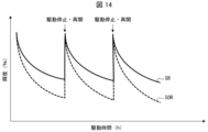
- FIG. 14 shows the degree of luminance reduction due to charge-up of quantum dots QD when a red light-emitting element 5R including a red light-emitting layer 24REM formed using a quantum dot solution with a concentration of 0.01 M from among the multiple types of quantum dot solutions shown in FIG. 7, and a red light-emitting element 50R as a comparative example shown in FIG. 10 are driven intermittently.
- the comparative red light-emitting element 50R experiences a large temporary drop in luminance during the drive period, which is a constant period of continuous current flow, compared to the red light-emitting element 5R.
- This temporary drop in luminance during the drive period which is a constant period of continuous current flow, is due to charge-up of the quantum dots QD, and is a reversible drop in luminance that can be resolved by applying a reverse voltage or leaving it unpowered.
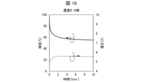
- FIG. 18 shows the degree of change in luminance and voltage over the operating time of a red light-emitting element 5R including a red light-emitting layer 24REM formed using a quantum dot solution with a concentration of 0.04 M from among the multiple types of quantum dot solutions shown in FIG. 7.
- FIG. 19 shows the degree of change in luminance and voltage over the operating time of a red light-emitting element 5R including a red light-emitting layer 24REM formed using a quantum dot solution with a concentration of 0.08 M from among the multiple types of quantum dot solutions shown in FIG. 7.
- the initial luminance decrease rate (e.g., luminance decrease rate within 1 hour) of the red light emitting element 5R including the red light emitting layer 24REM formed using the quantum dot solution having a concentration of 0.04 M shown in FIG. 18 is significantly reduced compared to the initial luminance decrease rate (e.g., luminance decrease rate within 1 hour) of the red light emitting element 5R including the red light emitting layer 24REM formed using the quantum dot solution having a concentration of 0.08 M shown in FIG. 19.
- the initial increase in drive voltage (e.g., the increase in drive voltage within 1 hour) of the red light emitting element 5R including the red light emitting layer 24REM formed using the quantum dot solution having a concentration of 0.04 M shown in FIG. 18 is significantly suppressed compared to the initial increase in drive voltage (e.g., the increase in drive voltage within 1 hour) of the red light emitting element 5R including the red light emitting layer 24REM formed using the quantum dot solution having a concentration of 0.08 M shown in FIG. 19.
- the initial luminance decrease rate e.g., luminance decrease rate within 1 hour
- the initial increase in driving voltage e.g., increase in driving voltage within 1 hour
- the luminance decrease rate after 5 hours of driving shown in FIG. 17 it is preferable to form the red light-emitting layer 24REM using a quantum dot solution having a concentration [M] of 0.04, 0.02, 0.01, or 0.005 from among the multiple types of quantum dot solutions shown in FIG. 7.
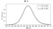
- Figure 15 shows the PL intensity (photoluminescence intensity) at each wavelength for a red light-emitting layer 24REM formed using a quantum dot solution with a concentration of 0.01 M from among the multiple types of quantum dot solutions shown in Figure 7, and a red light-emitting layer formed using a quantum dot solution with a concentration of 0.16 M as a comparative example.
- the emission peak wavelength of the red light-emitting layer formed using a quantum dot solution with a concentration of 0.16 M which is a comparative example, is 632 nm
- the emission peak wavelength of the red light-emitting layer 24REM formed using a quantum dot solution with a concentration of 0.01 M is 634 nm.
- This shift in the emission peak wavelength to the long wavelength side is believed to be due to an increase in Forster resonance energy transfer (FRET).
- FRET Forster resonance energy transfer
- the emission peak wavelengths of the red light-emitting layers 24REM formed using quantum dot solutions with concentrations of 0.02M, 0.04M, and 0.08M are all 632 nm, and no shift in the emission peak wavelength to the long wavelength side is observed. This is believed to be because, in the case of the red light-emitting layers 24REM formed using quantum dot solutions with concentrations of 0.02M, 0.04M, and 0.08M, respectively, the distance between the cores of the quantum dots QD can be secured to a certain level or more, and Forster resonance energy transfer (FRET) can be suppressed.
- FRET Forster resonance energy transfer
- the distance between the cores of the quantum dots QD cannot be secured to a certain level or more, and it is believed that the emission peak wavelength shifts to the long wavelength side due to the increase in Forster resonance energy transfer (FRET).
- FRET Forster resonance energy transfer
- the red light-emitting layer 24REM using a quantum dot solution having a concentration [M] of 0.08, 0.04, 0.02, or 0.01 from among the multiple types of quantum dot solutions shown in Figure 7.
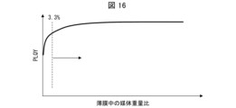
- Figure 16 shows the relationship between the weight ratio of the continuous film MR containing metal sulfide, which is the medium in the multiple types of red light-emitting layers 24REM, which are thin films formed using the multiple types of quantum dot solutions shown in Figure 7, and the internal quantum yield (PLQY).
- the ZnS medium weight ratio in the red light emitting layer 24REM is 3.3%
- the internal quantum yield (PLQY) is a good value of 60%.
- the ZnS medium weight ratio in the red light emitting layer 24REM is 6.4% to 35.4%
- the internal quantum yield (PLQY) is a good value of 74% to 76%.
- the red light-emitting layer 24REM using a quantum dot solution having a concentration [M] of 0.08, 0.04, 0.02, 0.01, or 0.005 from among the multiple types of quantum dot solutions shown in Figure 7.
- the weight ratio of the ZnS medium in the red light-emitting layer 24REM is greater than 3.3% and less than 35%, and for example, it is preferable to form the red light-emitting layer 24REM using a quantum dot solution having a concentration [M] of 0.04, 0.02, or 0.01 from the multiple types of quantum dot solutions shown in Figure 7.
- a red light emitting element 5R including a red light emitting layer 24REM formed using a quantum dot solution with a concentration [M] of 0.04, 0.02, or 0.01 the shift in the emission peak wavelength can be suppressed to 0-2 nm, the internal quantum yield (PLQY) can be achieved to 74%-76%, the maximum external quantum efficiency (maximum EQE) can be achieved to 7.6%-7.9%, and the luminance reduction rate after 5 hours of operation can be suppressed to 28%-44%.
- the weight ratio of the ZnS medium in the red light-emitting layer 24REM is greater than 3.3% and less than 35%, in a cross section of a portion of the red light-emitting layer 24REM including a cross section of a predetermined number, for example, 50 or more quantum dots QDs, among the multiple quantum dots QDs included in the red light-emitting layer 24REM, the cross-sectional area A of the continuous film MR including the metal sulfide matrix is 3.4% or more and 27.0% or less of the combined area B of the cross sections of the predetermined number, for example, 50 or more quantum dots QDs.
- the volume of the continuous film MR containing metal sulfide, which is the matrix in the red light-emitting layer 24REM is 3.6% or more and 37.1% or less of the volume of the red light-emitting layer 24REM.
- the preferred volume value of the continuous film MR containing metal sulfide relative to the volume of the red light emitting layer 24REM described above can be calculated, for example, as follows.
- InP with a density of 4.81 g/cm 3 is used as the core material of the quantum dot QD
- ZnS with a density of 4.09 g/cm 3 is used as the shell material of the quantum dot QD. If the diameter of the core of the quantum dot QD is 3.2 nm and the thickness of the shell of the quantum dot QD is 0.5 nm, the average density of the quantum dot QD can be 4.41 g/cm 3.
- the ZnS medium is mixed with 15 mg of quantum dot QD at a lower limit of 0.005 M, the weight of the ZnS medium is 3.3% and the volume of the ZnS medium is 3.6%.
- the ZnS medium is mixed with 15 mg of quantum dot QD at an upper limit of 0.08 M, the weight of the ZnS medium is 35.4% and the volume of the ZnS medium is 37.1%.
- the preferred area A of the cross section of the continuous film MR containing metal sulfide relative to the total area B of the cross sections of the above-mentioned predetermined number, for example, 50 or more quantum dots QD can be calculated, for example, as follows. If the volume of the quantum dots QD is V(QD) and the volume of the ZnS medium is V(MR), the volume V(24REM) of the red light emitting layer 24REM is V(QD)+V(MR). If the thickness of the sample when observed with a transmission electron microscope (TEM) (thickness in the depth direction in FIG.
- TEM transmission electron microscope
- the radius r of the quantum dots QD is the radius r of the quantum dots QD
- the cross-sectional area of the quantum dots QD is ((V(QD)+V(MR))/r).
- the radius of the quantum dot QD is r
- the volume V(QD) of each of the n quantum dots QD is 4/3 ⁇ r3
- the maximum cross-sectional area of the quantum dot QD is ⁇ r2
- the total cross-sectional area of the n quantum dots QD cut at random positions is 0.66n ⁇ r2 .
- the cross-sectional area of the ZnS medium is 3.4% of the red light-emitting layer 24REM, and when the volume of the ZnS medium is 37.1% of the red light-emitting layer 24REM, the cross-sectional area of the ZnS medium is 27.0% of the entire red light-emitting layer 24REM.
- a transmission electron microscope (TEM) image of a cross section of a portion of the red light-emitting layer 24REM including cross sections of 50 or more quantum dots QDs out of the multiple quantum dots QDs includes a first region having a higher electron density corresponding to the area of the cross section of the continuous film MR including metal sulfide and having an area corresponding to the combined area of the cross sections of the 50 or more quantum dots QDs and having a lower electron density
- the red light-emitting layer 24REM has a width L perpendicular to the cross section of the red light-emitting layer 24REM
- the product D of the area of the first region and the width L and the product E of the area of the second region and the width L are the volume of the portion of the red light-emitting layer 24REM
- the product D may be the volume of the continuous film MR including metal sulfide that is a matrix in the portion of the red light-emitting layer 24REM.
- the red light-emitting layer 24REM includes a first region having a specific diffraction peak due to X-ray diffraction of a metal sulfide and a second region having a specific diffraction peak due to X-ray diffraction of quantum dots QD, the area of the first region in the cross section of the red light-emitting layer 24REM calculated based on the specific diffraction peak due to X-ray diffraction of the metal sulfide is area G, the area of the second region in the cross section of the red light-emitting layer 24REM calculated based on the specific diffraction peak due to X-ray diffraction of the quantum dots is area H, the red light-emitting layer 24REM has a width L perpendicular to the cross section of the red light-emitting layer 24REM, the product I of the area G and the width L and the product J of the area H and the width L are added together to form a volume of a portion of the red light-e
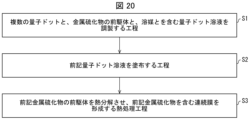
- FIG. 20 is a diagram for explaining the process of forming the red light-emitting layer 24REM included in the manufacturing method of the red light-emitting element 5R provided in the display device 1 of this embodiment.
- the process for forming the red light-emitting layer 24REM included in the manufacturing method of the red light-emitting element 5R included in the display device 1 includes a process (S1) for preparing a quantum dot solution containing a plurality of quantum dots QD, a metal sulfide precursor, and a solvent, a process (S2) for applying the quantum dot solution, and a heat treatment process (S3) for thermally decomposing the metal sulfide precursor to form a continuous film MR containing the metal sulfide as a matrix.
- the amount of the multiple quantum dots and the amount of the metal sulfide precursor contained in the quantum dot solution are adjusted so that the value of ((weight of red light-emitting layer 24REM-weight of quantum dots QD)/weight of red light-emitting layer 24REM) x 100% in the red light-emitting layer 24REM after the heat treatment step (S3) is greater than 3.3% and less than 35%.
- the method for manufacturing the red light-emitting element 5R includes a step of forming one of the anode 22 and the cathode 25, a step of forming the red light-emitting layer 24REM described above, and a step of forming the other of the anode 22 and the cathode 25.
- the configuration and manufacturing method have been described using the red light-emitting element 5R as an example, but the configuration and manufacturing method can also be applied to the green light-emitting element 5G and blue light-emitting element 5B in the same manner.
- This disclosure can be used in light-emitting devices, display devices, methods for manufacturing light-emitting devices, and methods for forming light-emitting layers.
Landscapes
- Engineering & Computer Science (AREA)
- Manufacturing & Machinery (AREA)
- Chemical & Material Sciences (AREA)
- Crystallography & Structural Chemistry (AREA)
- Inorganic Chemistry (AREA)
- Nanotechnology (AREA)
- Physics & Mathematics (AREA)
- Optics & Photonics (AREA)
- Electroluminescent Light Sources (AREA)
Priority Applications (3)
| Application Number | Priority Date | Filing Date | Title |
|---|---|---|---|
| CN202380097298.XA CN121058349A (zh) | 2023-04-18 | 2023-04-18 | 发光元件、显示装置、发光元件的制造方法及发光层的形成方法 |
| JP2025514911A JP7840491B2 (ja) | 2023-04-18 | 2023-04-18 | 発光素子、表示装置、発光素子の製造方法及び発光層の形成方法 |
| PCT/JP2023/015421 WO2024218846A1 (ja) | 2023-04-18 | 2023-04-18 | 発光素子、表示装置、発光素子の製造方法及び発光層の形成方法 |
Applications Claiming Priority (1)
| Application Number | Priority Date | Filing Date | Title |
|---|---|---|---|
| PCT/JP2023/015421 WO2024218846A1 (ja) | 2023-04-18 | 2023-04-18 | 発光素子、表示装置、発光素子の製造方法及び発光層の形成方法 |
Publications (1)
| Publication Number | Publication Date |
|---|---|
| WO2024218846A1 true WO2024218846A1 (ja) | 2024-10-24 |
Family
ID=93152408
Family Applications (1)
| Application Number | Title | Priority Date | Filing Date |
|---|---|---|---|
| PCT/JP2023/015421 Ceased WO2024218846A1 (ja) | 2023-04-18 | 2023-04-18 | 発光素子、表示装置、発光素子の製造方法及び発光層の形成方法 |
Country Status (3)
| Country | Link |
|---|---|
| JP (1) | JP7840491B2 (cg-RX-API-DMAC7.html) |
| CN (1) | CN121058349A (cg-RX-API-DMAC7.html) |
| WO (1) | WO2024218846A1 (cg-RX-API-DMAC7.html) |
Cited By (1)
| Publication number | Priority date | Publication date | Assignee | Title |
|---|---|---|---|---|
| WO2026163940A1 (ja) * | 2025-01-31 | 2026-08-06 | 東レ株式会社 | 着色樹脂組成物、着色膜、ブラックマトリクス、カラーフィルターおよび有機el表示装置 |
Citations (7)
| Publication number | Priority date | Publication date | Assignee | Title |
|---|---|---|---|---|
| JP2010526420A (ja) * | 2007-05-07 | 2010-07-29 | イーストマン コダック カンパニー | 電力の分配が改善されたエレクトロルミネッセンス・デバイス |
| JP2017505842A (ja) * | 2014-02-04 | 2017-02-23 | コーニンクレッカ フィリップス エヌ ヴェKoninklijke Philips N.V. | 無機マトリクス内に無機リガンドを有する量子ドット |
| KR20170105156A (ko) * | 2016-03-08 | 2017-09-19 | 삼성디스플레이 주식회사 | 발광 소자 및 이의 제조 방법 |
| US20180198034A1 (en) * | 2015-08-07 | 2018-07-12 | Osram Opto Semiconductors Gmbh | Optoelectronic component comprising a conversion element, method of producing an optoelectronic component comprising a conversion element, and use of an optoelectronic component comprising a conversion element |
| CN110003884A (zh) * | 2019-03-14 | 2019-07-12 | 纳晶科技股份有限公司 | 掺杂量子点及其制备方法、量子点光电器件 |
| US20210135138A1 (en) * | 2019-10-31 | 2021-05-06 | Samsung Electronics Co., Ltd. | Light emitting device, production method thereof, and display device including the same |
| JP2022530420A (ja) * | 2019-04-24 | 2022-06-29 | ネクスドット | 半導体粒子を含む安定化されたインクおよびその使用 |
Family Cites Families (1)
| Publication number | Priority date | Publication date | Assignee | Title |
|---|---|---|---|---|
| JP6454717B2 (ja) * | 2014-02-04 | 2019-01-16 | コーニンクレッカ フィリップス エヌ ヴェKoninklijke Philips N.V. | 量子ドットのオキソ系及び水酸基系の複合無機リガンド |
-
2023
- 2023-04-18 CN CN202380097298.XA patent/CN121058349A/zh active Pending
- 2023-04-18 WO PCT/JP2023/015421 patent/WO2024218846A1/ja not_active Ceased
- 2023-04-18 JP JP2025514911A patent/JP7840491B2/ja active Active
Patent Citations (7)
| Publication number | Priority date | Publication date | Assignee | Title |
|---|---|---|---|---|
| JP2010526420A (ja) * | 2007-05-07 | 2010-07-29 | イーストマン コダック カンパニー | 電力の分配が改善されたエレクトロルミネッセンス・デバイス |
| JP2017505842A (ja) * | 2014-02-04 | 2017-02-23 | コーニンクレッカ フィリップス エヌ ヴェKoninklijke Philips N.V. | 無機マトリクス内に無機リガンドを有する量子ドット |
| US20180198034A1 (en) * | 2015-08-07 | 2018-07-12 | Osram Opto Semiconductors Gmbh | Optoelectronic component comprising a conversion element, method of producing an optoelectronic component comprising a conversion element, and use of an optoelectronic component comprising a conversion element |
| KR20170105156A (ko) * | 2016-03-08 | 2017-09-19 | 삼성디스플레이 주식회사 | 발광 소자 및 이의 제조 방법 |
| CN110003884A (zh) * | 2019-03-14 | 2019-07-12 | 纳晶科技股份有限公司 | 掺杂量子点及其制备方法、量子点光电器件 |
| JP2022530420A (ja) * | 2019-04-24 | 2022-06-29 | ネクスドット | 半導体粒子を含む安定化されたインクおよびその使用 |
| US20210135138A1 (en) * | 2019-10-31 | 2021-05-06 | Samsung Electronics Co., Ltd. | Light emitting device, production method thereof, and display device including the same |
Cited By (1)
| Publication number | Priority date | Publication date | Assignee | Title |
|---|---|---|---|---|
| WO2026163940A1 (ja) * | 2025-01-31 | 2026-08-06 | 東レ株式会社 | 着色樹脂組成物、着色膜、ブラックマトリクス、カラーフィルターおよび有機el表示装置 |
Also Published As
| Publication number | Publication date |
|---|---|
| JP7840491B2 (ja) | 2026-04-03 |
| JPWO2024218846A1 (cg-RX-API-DMAC7.html) | 2024-10-24 |
| CN121058349A (zh) | 2025-12-02 |
Similar Documents
| Publication | Publication Date | Title |
|---|---|---|
| KR101274068B1 (ko) | 양자점 발광 소자 및 이를 이용한 디스플레이 | |
| US20240373660A1 (en) | Light-emitting element, method for manufacturing light-emitting element, and display device | |
| JP7818094B2 (ja) | 発光素子、表示装置、発光素子の製造方法 | |
| JP7733837B2 (ja) | 発光素子および表示装置 | |
| JP7840491B2 (ja) | 発光素子、表示装置、発光素子の製造方法及び発光層の形成方法 | |
| US20260082762A1 (en) | Light-emitting element and display device | |
| WO2023233646A1 (ja) | 発光素子、表示デバイス、発光素子の製造方法、表示デバイスの製造方法 | |
| WO2024084572A1 (ja) | 発光素子、表示装置及び発光層の形成方法 | |
| JP7656781B2 (ja) | 発光素子、及び表示装置 | |
| WO2024079908A1 (ja) | 発光素子および表示装置並びに発光素子の製造方法 | |
| WO2024018509A1 (ja) | 発光素子、表示装置、および発光素子の製造方法 | |
| JP7858919B2 (ja) | 発光素子、表示装置及び発光層の形成方法 | |
| WO2024201569A1 (ja) | 発光素子、表示装置、発光素子の製造方法及び発光素子の発光特性の回復方法 | |
| WO2024201571A1 (ja) | 発光素子及び表示装置 | |
| WO2024018508A1 (ja) | 発光素子、表示装置、発光素子の製造方法及び発光素子の発光特性の回復方法 | |
| US20260049244A1 (en) | Light-emitting element, display device, and method for producing light-emitting element | |
| WO2025215732A1 (ja) | 発光素子、表示装置、及び表示装置の製造方法 | |
| WO2024209670A1 (ja) | 発光素子および表示装置 | |
| WO2025215733A1 (ja) | 発光素子及び表示装置 | |
| WO2025215730A1 (ja) | 発光素子及び表示装置 | |
| WO2025182059A1 (ja) | 発光素子及び表示装置 | |
| WO2024075248A1 (ja) | 発光素子、表示装置及び発光層の形成方法 | |
| WO2025224963A1 (ja) | 発光素子及び表示装置 | |
| US20260068428A1 (en) | Light-emitting element, and display device | |
| WO2026058408A1 (ja) | 表示装置、及び表示装置の製造方法 |
Legal Events
| Date | Code | Title | Description |
|---|---|---|---|
| 121 | Ep: the epo has been informed by wipo that ep was designated in this application |
Ref document number: 23933993 Country of ref document: EP Kind code of ref document: A1 |
|
| ENP | Entry into the national phase |
Ref document number: 2025514911 Country of ref document: JP Kind code of ref document: A |
|
| WWE | Wipo information: entry into national phase |
Ref document number: 2025514911 Country of ref document: JP |
|
| NENP | Non-entry into the national phase |
Ref country code: DE |
|
| 122 | Ep: pct application non-entry in european phase |
Ref document number: 23933993 Country of ref document: EP Kind code of ref document: A1 |