WO2024214501A1 - 半導体装置及び電力変換装置 - Google Patents
半導体装置及び電力変換装置 Download PDFInfo
- Publication number
- WO2024214501A1 WO2024214501A1 PCT/JP2024/010727 JP2024010727W WO2024214501A1 WO 2024214501 A1 WO2024214501 A1 WO 2024214501A1 JP 2024010727 W JP2024010727 W JP 2024010727W WO 2024214501 A1 WO2024214501 A1 WO 2024214501A1
- Authority
- WO
- WIPO (PCT)
- Prior art keywords
- insulating film
- semiconductor device
- electrode
- interlayer insulating
- region
- Prior art date
- Legal status (The legal status is an assumption and is not a legal conclusion. Google has not performed a legal analysis and makes no representation as to the accuracy of the status listed.)
- Ceased
Links
Images













Classifications
-
- H—ELECTRICITY
- H10—SEMICONDUCTOR DEVICES; ELECTRIC SOLID-STATE DEVICES NOT OTHERWISE PROVIDED FOR
- H10D—INORGANIC ELECTRIC SEMICONDUCTOR DEVICES
- H10D30/00—Field-effect transistors [FET]
- H10D30/01—Manufacture or treatment
- H10D30/021—Manufacture or treatment of FETs having insulated gates [IGFET]
-
- H—ELECTRICITY
- H10—SEMICONDUCTOR DEVICES; ELECTRIC SOLID-STATE DEVICES NOT OTHERWISE PROVIDED FOR
- H10D—INORGANIC ELECTRIC SEMICONDUCTOR DEVICES
- H10D30/00—Field-effect transistors [FET]
- H10D30/60—Insulated-gate field-effect transistors [IGFET]
-
- H—ELECTRICITY
- H10—SEMICONDUCTOR DEVICES; ELECTRIC SOLID-STATE DEVICES NOT OTHERWISE PROVIDED FOR
- H10D—INORGANIC ELECTRIC SEMICONDUCTOR DEVICES
- H10D8/00—Diodes
- H10D8/60—Schottky-barrier diodes
Definitions
- This disclosure relates to semiconductor devices and power conversion devices.
- SiC silicon carbide
- MOSFETs Metal Oxide Semiconductor Field Effect Transistors
- IGBTs Insulated Gate Bipolar Transistors
- a SiC MOSFET with a breakdown voltage of 1 to 1.2 kV can have an on-resistance of 2 m ⁇ cm 2 or less, which is half or less of the resistance of a Si MOSFET and IGBT with the same breakdown voltage.
- the on-resistance of a SiC semiconductor device can be significantly reduced compared to a Si semiconductor device is that the SiC semiconductor device has a high dielectric breakdown field, the breakdown voltage layer (i.e., the drift layer) for achieving the same breakdown voltage can be made thinner compared to a Si semiconductor device, and the impurity doping amount of the breakdown voltage layer can be increased.
- the breakdown voltage layer i.e., the drift layer
- a forward current i.e., a bipolar current
- the recombination energy increases when the minority carriers injected by the current flow through the PN diode recombine with the majority carriers.
- stacking faults which are planar defects, expand, starting from basal plane dislocations present in the SiC substrate.
- the current decreases and the forward voltage increases, i.e., the forward voltage shifts, causing a decrease in the performance of the semiconductor device and ultimately a decrease in reliability.
- Patent Document 1 proposes providing a p+ type semiconductor region, which is a hole extraction region, so as to surround an active region in which a MOSFET is provided in a semiconductor substrate including an n - type SiC substrate and an epitaxial growth layer on the SiC substrate.
- Patent Documents 2 and 3 also propose incorporating an SBD (Schottky Barrier Diode) as a unipolar diode in the same semiconductor chip as the MOSFET.
- SBD Schottky Barrier Diode
- the present disclosure has been made in consideration of the above-mentioned problems, and aims to provide technology that can improve the reliability of semiconductor devices.
- the semiconductor device comprises a semiconductor substrate, a first insulating film provided on a reference surface of the semiconductor substrate, a first electrode provided on the first insulating film, a second insulating film covering the reference surface, the first insulating film, and the first electrode, and a second electrode covering the reference surface and the second insulating film, the side surface of the second insulating film includes a plurality of partial side surfaces that form different angles with the reference surface, and a second angle formed between the partial side surface of the plurality of partial side surfaces that corresponds in height to the first side surface and the reference surface is smaller than a first angle formed between the first side surface of the first electrode and the reference surface.
- the second angle between the reference plane and a partial side surface of the plurality of partial side surfaces that corresponds in height to the first side surface is smaller than the first angle between the first side surface of the first electrode and the reference plane.
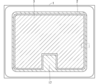
- 1 is a top view showing a configuration of a semiconductor device according to a first embodiment
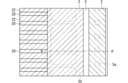
- 1 is a top view showing a configuration of a semiconductor device according to a first embodiment
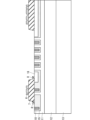
- 1 is a schematic cross-sectional view showing a configuration of a semiconductor device according to a first embodiment
- 2 is a flowchart showing a method for manufacturing the semiconductor device according to the first embodiment.
- 3A to 3C are schematic cross-sectional views showing a manufacturing process of the semiconductor device according to the first embodiment.
- 3A to 3C are schematic cross-sectional views showing a manufacturing process of the semiconductor device according to the first embodiment.
- 3A to 3C are schematic cross-sectional views showing a manufacturing process of the semiconductor device according to the first embodiment.
- 3A to 3C are schematic cross-sectional views showing a manufacturing process of the semiconductor device according to the first embodiment.
- 3A to 3C are schematic cross-sectional views showing a manufacturing process of the semiconductor device according to the first embodiment.
- 3A to 3C are schematic cross-sectional views showing a manufacturing process of the semiconductor device according to the first embodiment.
- 3A to 3C are schematic cross-sectional views showing a manufacturing process of the semiconductor device according to the first embodiment.
- 3A to 3C are schematic cross-sectional views showing a manufacturing process of the semiconductor device according to the first embodiment.
- 3A to 3C are schematic cross-sectional views showing a manufacturing process of the semiconductor device according to the first embodiment.
- 2A to 2C are schematic cross-sectional views showing a manufacturing process of the semiconductor device according to the first embodiment.
- 3A to 3C are schematic cross-sectional views showing a manufacturing process of the semiconductor device according to the first embodiment.
- 3A to 3C are schematic cross-sectional views showing a manufacturing process of the semiconductor device according to the first embodiment.
- 3A to 3C are schematic cross-sectional views showing a manufacturing process of the semiconductor device according to the first embodiment.
- 1 is a schematic cross-sectional view showing a configuration of a semiconductor module according to a first embodiment
- 1A and 1B are a schematic cross-sectional view and an SEM photograph showing a configuration of a semiconductor device according to a first embodiment
- 11A and 11B are diagrams showing test results of the semiconductor device according to the first embodiment
- 11A and 11B are diagrams showing test results of the semiconductor device according to the first embodiment
- 1 is a schematic cross-sectional view showing a configuration of a semiconductor device according to a modification of the first embodiment
- FIG. 11 is a schematic cross-sectional view showing a configuration of a semiconductor device according to a second embodiment.
- 11A to 11C are cross-sectional views illustrating a manufacturing process of a semiconductor device according to a second embodiment.
- FIG. 11A to 11C are cross-sectional views illustrating a manufacturing process of a semiconductor device according to a second embodiment.
- 11A to 11C are cross-sectional views illustrating a manufacturing process of a semiconductor device according to a second embodiment.
- FIG. 11 is a schematic cross-sectional view showing a configuration of a semiconductor device according to a modification of the second embodiment.
- FIG. 11 is a cross-sectional view showing a configuration of a semiconductor device according to a third embodiment.
- FIG. 13 is a top view showing a configuration of a semiconductor device according to a fourth embodiment.
- FIG. 13 is a schematic cross-sectional view showing a configuration of a semiconductor device according to a fourth embodiment.
- 13 is a flowchart showing a method for manufacturing a semiconductor device according to a fourth embodiment.
- FIGS. 13A to 13C are cross-sectional views illustrating a manufacturing process of a semiconductor device according to a fourth embodiment.
- 13A to 13C are cross-sectional views illustrating a manufacturing process of a semiconductor device according to a fourth embodiment.
- FIG. 13 is a schematic cross-sectional view showing a configuration of a semiconductor device according to a fourth embodiment.
- FIG. 13 is a block diagram showing a configuration of a power conversion system to which a power conversion device according to a fifth embodiment is applied.
- a certain part having a higher density than another part means, for example, that the average density of the certain part is higher than the average density of the other part.
- a certain part having a lower density than another part means, for example, that the average density of the certain part is lower than the average density of the other part.
- the semiconductor device according to the first embodiment is a power semiconductor device, made of an n-type SiC substrate, and a planar gate type MOSFET (Metal Oxide Semiconductor Field Effect Transistor) incorporating an SBD (Schottky Barrier Diode).
- MOSFET Metal Oxide Semiconductor Field Effect Transistor
- SBD Schottky Barrier Diode
- the semiconductor device is not limited to this, and may be, for example, a trench gate type semiconductor device, an IGBT (Insulated Gate Bipolar Transistor), or an RC-IGBT (Reverse Conducting - IGBT).
- FIG. 1 is a top view showing the configuration of a semiconductor device 1 according to the first embodiment.
- a source electrode 3 located in the center and a gate wiring 2 surrounding the source electrode 3 are provided on the upper part of the semiconductor device 1.
- a gate pad 17 is provided between the center and the end of the upper part of the semiconductor device 1 and is electrically connected to the gate wiring 2.
- the gate wiring 2 and the gate pad 17 are separated and insulated from the source electrode 3.
- the region where unit cells are periodically arranged is defined as an active region, and the region other than the active region is defined as a termination region.
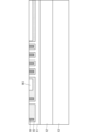
- FIG. 2 is an enlarged top view of a portion between the active region and the termination region, indicated by the dashed line in FIG. 1.
- the active region includes an SBD region 20 in which an SBD is provided, and a MOS region 22 in which a MOSFET is provided, and the SBD region 20 and the MOS region 22 are provided in a stripe pattern.
- the second interlayer insulating film 5 is provided in a region other than the active region including the multiple SBD regions 20 and multiple MOS regions 22, i.e., the termination region.
- the gate wiring 2 and source electrode 3 are provided on the second interlayer insulating film 5, and the second interlayer insulating film 5 has a gate contact hole 5a covered by the gate wiring 2 and a contact hole 5b covered by the source electrode 3.
- an SBD is provided below the contact hole 5b in the termination region, similar to the SBD region 20 in the active region.
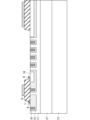
- FIG. 3 is a schematic cross-sectional view showing the configuration of a portion taken along line a-a' in FIG. 2.
- the second interlayer insulating film 5 is provided in the termination region, so FIG. 3 generally shows the configuration of the termination region.
- Line a-a' in FIG. 2 crosses over contact hole 5b in the second interlayer insulating film 5, so in FIG. 3, the second interlayer insulating film 5 is shown in two locations on either side of contact hole 5b.
- the semiconductor device 1 includes an n-type SiC substrate 13, an n-type epitaxial growth layer 12, an n-type well region 11, a p-type well region 15, a p-type potential fixed layer 10, an n-type source region 16, a contact region 9, a first interlayer insulating film 7, a gate electrode 6, a second interlayer insulating film 5, a barrier metal layer 4, a source electrode 3, a gate wiring 2, and a drain electrode 14 in the termination region.
- the semiconductor substrate 1a includes a SiC substrate 13 and an epitaxial growth layer 12.
- the semiconductor substrate 1a is not limited thereto.
- the semiconductor substrate 1a may include the epitaxial growth layer 12 without including the SiC substrate 13, or may include the SiC substrate 13 without including the epitaxial growth layer 12.
- the epitaxial growth layer 12 is uniformly provided on the first main surface (top surface in FIG. 3) of the SiC substrate 13, and the n-type well region 11 is provided on the epitaxial growth layer 12.
- the p-type well region 15 is selectively provided on the upper part of the n-type well region 11.
- the sides and bottom of the potential fixing layer 10 are provided so as to be covered by the p-type well region 15, and the sides and bottom of the source region 16 are provided so as to be covered by the p-type well region 15.
- the first insulating film, the first interlayer insulating film 7, is provided on the reference surface of the semiconductor substrate 1a.
- the reference surface is the top surface
- the first interlayer insulating film 7 is selectively provided on the potential fixing layer 10, the n-type well region 11, the p-type well region 15, and the source region 16 in the termination region.
- the first interlayer insulating film 7 has contact holes 5b, just like the second interlayer insulating film 5, so in FIG. 3, the first interlayer insulating film 7 is shown in two places, just like the second interlayer insulating film 5.
- the region located on the opposite side of the active region with respect to the gate electrode 6 provided on the first interlayer insulating film 7 on the active region side will be referred to as the reverse region.
- the gate electrode 6 is electrically connected to a gate electrode (not shown) provided in the MOS region 22 in FIG. 2, and is at the same potential as the gate electrode in the MOS region 22.
- a voltage equal to or greater than the threshold voltage is applied to the gate electrode in the MOS region 22, the conductivity type of a portion of the p-type semiconductor layer sandwiched between the n-type semiconductor layers is inverted, and a channel is formed in that portion.
- the configuration in FIG. 3 is not a MOS region 22, so the gate electrode 6 in FIG. 3 indirectly forms a channel in the p-type semiconductor layer in the MOS region, but does not directly form a channel in the p-type semiconductor layer in FIG. 3.
- the second insulating film, the second interlayer insulating film 5, is provided to cover the reference surface of the semiconductor substrate 1a, the first interlayer insulating film 7, and the gate electrode 6.
- the second interlayer insulating film 5 has a gate contact hole 5a that partially exposes the gate electrode 6 provided on the first interlayer insulating film 7 on the reverse region side, and a contact hole 5b that partially exposes the n-type well region 11 in the termination region.
- the barrier metal layer 4 covers the potential fixing layer 10, the n-type well region 11, the p-type well region 15, the source region 16, the second interlayer insulating film 5, and the gate electrode 6 exposed from the gate contact hole 5a.
- the barrier metal layer 4 connected to the gate electrode 6 is separated and insulated from the barrier metal layer 4 covering the n-type well region 11, etc.
- the contact region 9 is provided between the barrier metal layer 4 and one of the source region 16, the p-type well region 15, and the potential fixing layer 10 provided on the active region side of the first interlayer insulating film 7, and provides an ohmic connection between them.
- the gate wiring 2 is electrically connected to the gate electrode 6 via the barrier metal layer 4 that covers the gate electrode 6 exposed from the gate contact hole 5a.
- the source electrode 3 is electrically connected to the n-type well region 11 and the like via the barrier metal layer 4 that covers the n-type well region 11 and the like.
- the drain electrode 14 is provided on the second main surface (the bottom surface in FIG. 3) of the SiC substrate 13, which is opposite to the first main surface on which the epitaxial growth layer 12 is provided.
- the side of the second interlayer insulating film 5 includes a plurality of partial side surfaces that form different angles with a reference plane (top surface in FIG. 3) of the semiconductor substrate 1a.
- a second angle formed between a partial side surface of the plurality of partial side surfaces that corresponds in height to the first side surface and the reference plane is smaller than a first angle formed between the first side surface of the gate electrode 6 and the reference plane.
- a fourth angle formed between a partial side surface of the plurality of partial side surfaces that corresponds in height to the second side surface and the reference plane is larger than a third angle formed between the second side surface of the first interlayer insulating film 7 and the reference plane.
- ⁇ Production Method> 4 is a flowchart showing a method for manufacturing the semiconductor device 1 according to the first preferred embodiment. Each of the steps from the semiconductor substrate preparation step S1 to the drain electrode formation step S13 will be described below.
- an epitaxial growth layer 12 made of n-type SiC is formed by CVD (Chemical Vapor Deposition) on a first main surface of an n-type SiC substrate 13 having a polytype of 4H.
- the n-type impurity concentration of the epitaxial growth layer 12 is, for example, 1 ⁇ 10 15 cm ⁇ 3 to 1 ⁇ 10 17 cm ⁇ 3 .
- the thickness of the epitaxial growth layer 12 is, for example, 5 ⁇ m to 50 ⁇ m.
- the SiC substrate 13 has an n-type, but the SiC substrate 13 may have a p-type.
- impurities are ion-implanted into the upper part of the epitaxial growth layer 12 to form the n-type well region 11.
- the impurity concentration of the n-type well region 11 is higher than the impurity concentration of the epitaxial growth layer 12.
- an implantation mask is formed in a predetermined region of the n-type well region 11 using photoresist or the like, and then p-type impurities are ion-implanted to form the p-type well region 15.
- the p-type impurities are, for example, B (boron) and Al (aluminum).
- the implantation depth of the p-type well region 15 is shallower than the depth of the n-type well region 11.
- the impurity concentration of the p-type well region 15 is, for example, 1 ⁇ 10 17 cm -3 to 1 ⁇ 10 19 cm -3 .
- an implantation mask is formed in a predetermined region of the p-type well region 15 using photoresist or the like, and then n-type impurities are ion-implanted to form the source region 16.
- the n-type impurities are, for example, phosphorus and nitrogen.
- the implantation depth of the source region 16 is shallower than that of the p-type well region 15.
- an implantation mask is formed in a predetermined region of the p-type well region 15 using photoresist or the like, and then p-type impurities are ion-implanted to form the potential fixing layer 10.
- the impurity concentration of the potential fixing layer 10 is higher than that of the p-type well region 15.
- the structure obtained in the step of FIG. 9 is annealed in a heat treatment device in an inert gas atmosphere such as Ar (argon) gas at a temperature of 1300 to 1900°C for 30 seconds to 1 hour. This annealing electrically activates the implanted p-type and n-type impurities.
- the first interlayer insulating film formation process S6 a CVD method is used to form an insulating film that will become the first interlayer insulating film 7, and the insulating film is then patterned using photolithography and dry or wet etching techniques. As a result, as shown in FIG. 10, the first interlayer insulating film 7 is formed, which remains in predetermined regions on the potential fixing layer 10, the n-type well region 11, the p-type well region 15, and the source region 16.
- the material for the first interlayer insulating film 7 is, for example, TEOS (Tetra EthOxy Silane).
- a gate oxide film is formed in the active region and the termination region.
- the gate oxide film in the active region insulates the gate electrode that forms a channel in the active region from the n-type and p-type semiconductor layers.
- the gate oxide film 8 is also provided in the termination region, but this is not limited thereto, and the gate oxide film 8 does not have to be provided in the termination region.
- a conductive film is deposited on the gate oxide film in the active region and on the first interlayer insulating film 7 in the termination region by thermal oxidation or CVD.
- the conductive film is then patterned using photolithography and dry or wet etching techniques.
- a gate electrode 6 is formed on the upper surface of the gate oxide film in the active region and on the upper surface of the first interlayer insulating film 7 in the termination region.
- the material of the conductive film that becomes the gate electrode 6 may be, for example, polycrystalline Si or poly-Si deposited by chemical vapor deposition or the like, or may be tungsten or tungsten silicide (WSi x ) when the semiconductor device 1 is to operate at a higher speed.
- the second interlayer insulating film formation process S9 an insulating film that will become the second interlayer insulating film 5 is formed using the CVD method, and then the insulating film is patterned using photolithography and dry or wet etching techniques. As a result, as shown in FIG. 13, the second interlayer insulating film 5 is formed, which covers the gate electrode 6 and the first interlayer insulating film 7 and has gate contact holes 5a and 5b. In this embodiment 1, the gate oxide film 8 becomes part of the second interlayer insulating film 5.
- the material of the second interlayer insulating film 5 is, for example, TEOS (tetra ethoxy silane) and BPSG (Boro-Phospho Silicate Glass).
- the contact region 9 is a nickel silicide layer formed, for example, by forming a metal film mainly composed of Ni (nickel) in an opening of a photoresist or the like by sputtering, and then performing a heat treatment at a temperature in the range of 600°C to 1100°C.
- a barrier metal layer 4 made of titanium or a titanium compound such as titanium nitride (TiN) is formed.
- a film of aluminum, an aluminum alloy made of aluminum and silicon, or nickel is formed to form the gate wiring 2 and the source electrode 3.
- the second main surface of the SiC substrate 13 is machined using a grinding wheel to thin the SiC substrate 13.
- a nickel film of, for example, about 600 nm is formed on the machined second main surface by appropriately using a sputtering method or the like to form the drain electrode 14.
- a nickel film of, for example, about 600 nm is formed on the machined second main surface by appropriately using a sputtering method or the like to form the drain electrode 14.
- a film containing a metal that has poor reactivity with the outside such as gold (Au) or silver (Ag)
- the drain electrode 14 may be a laminated film consisting of a nickel film and a protective film.
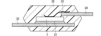
- the back side (i.e., the second main surface side) of the semiconductor device 1 is connected to a lead frame 32 via solder 31, and the front side (i.e., the first main surface side) of the semiconductor device 1 is connected to a lead frame 34 via a wire 33.
- the semiconductor device 1 and the wire 33 are sealed with molded resin 35, thereby completing a semiconductor module including the semiconductor device 1.
- a diode called a freewheel diode or a flywheel diode is connected in anti-parallel to an inductive load in order to suppress a rise in the source-drain voltage.
- a current flows through the aforementioned diode during freewheel operation.
- a semiconductor device 1 in which a BD (Body Diode) region or an SBD (Schottky Barrier Diode) region for passing current during such freewheel operation is provided in the termination region, heat is generated in the termination region of the semiconductor device 1.
- the temperature difference between when heat is being generated and when heat is not being generated in the termination region generates thermal stress in the gate electrode 6 and the second interlayer insulating film 5 that covers it due to the difference in linear expansion coefficients of various materials such as the gate electrode 6, the second interlayer insulating film 5 that covers it, and the source electrode 3 and mold resin 35 that surround it.
- This stress causes an external force to be applied to the gate electrode 6 through the second interlayer insulating film 5, which deteriorates the gate electrode 6 and causes a malfunction in the semiconductor device 1.
- the following describes how the semiconductor device 1 according to the first embodiment is able to suppress such malfunctions.
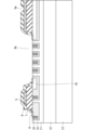
- FIG. 19 is a schematic diagram showing the configuration of the termination region of the semiconductor device 1 according to the first embodiment, and a SEM photograph of the configuration taken by a scanning electron microscope (SEM).
- the schematic diagram shows a first angle ⁇ gate1 , a second angle ⁇ insu2 , a third angle ⁇ insu3 , and a fourth angle ⁇ insu4 .
- ⁇ gate1 is an angle between the first side surface of the gate electrode 6 and a reference surface of the semiconductor substrate 1a, the angle being on the same side as the gate electrode 6.
- ⁇ gate1 is an angle between a tangent to a midpoint of the first side surface of the gate electrode 6 in the thickness direction of the gate electrode 6 (the up-down direction in the schematic diagram) and the reference surface of the semiconductor substrate 1a.
- ⁇ insu2 is the angle on the same side as the second interlayer insulating film 5, among the angles formed between a partial side surface of the second interlayer insulating film 5 having a height corresponding to the first side surface and a reference plane of the semiconductor substrate 1a.
- the reference plane is used as the reference for the height.
- ⁇ insu2 is the angle formed between a tangent to a partial side surface of the second interlayer insulating film 5 having a height corresponding to the midpoint portion and the reference plane of the semiconductor substrate 1a.
- the partial side surface having a height corresponding to the first side surface may be a partial side surface having the same height as the midpoint portion of the first side surface, or may be a partial side surface having substantially the same height as the midpoint portion of the first side surface.
- ⁇ insu3 is the angle between the second side surface of the first interlayer insulating film 7 and the reference surface of the semiconductor substrate 1a, the angle being on the same side as the first interlayer insulating film 7.
- ⁇ insu3 is the angle between the tangent to the lower part of the second side surface of the first interlayer insulating film 7 and the reference surface of the semiconductor substrate 1a.
- ⁇ insu4 is the angle on the same side as the second interlayer insulating film 5 among the angles formed between a partial side surface of the second interlayer insulating film 5, the height of which corresponds to the second side surface, and the reference plane of the semiconductor substrate 1a.
- ⁇ insu4 is the angle formed between a tangent to a partial side surface of the second interlayer insulating film 5, the height of which corresponds to the lower part of the second side surface, and the reference plane of the semiconductor substrate 1a.
- the partial side surface of the second side surface may be a partial side surface having the same height as the lower part of the second side surface, or may be a partial side surface having substantially the same height as the lower part of the second side surface.
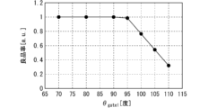
- Fig. 20 shows the relationship with the yield rate of the semiconductor module after 100,000 power cycle tests for ⁇ gate1
- Fig. 21 shows the relationship with the difference between ⁇ gate1 and ⁇ insu2 ( ⁇ gate1 - ⁇ insu2 ).
- FIG. 20 shows the yield rate of semiconductor modules after a power cycle test when the difference ( ⁇ gate1 - ⁇ insu2 ) is fixed at 20 degrees.
- ⁇ gate1 is 100 degrees or more
- the yield rate decreases.
- a defective module in which ⁇ gate1 is 100 degrees or more was analyzed, a crack was generated in the second interlayer insulating film 5 near the upper end of the gate electrode 6, and the source electrode 3 and the gate electrode 6 were electrically shorted. From this and the results of FIG. 20, it can be seen that when ⁇ gate1 is 95 degrees or less, insulation failure between the source and gate can be suppressed.
- FIG. 21 shows the yield rate of the semiconductor module after the power cycle test when ⁇ gate1 is fixed at 90 degrees.
- ⁇ gate1 - ⁇ insu2 >0 that is, when ⁇ insu2 is smaller than ⁇ gate1 , the yield rate increases. This is considered to be because the external force from various materials such as the source electrode 3 and the mold resin 35 surrounding the gate electrode 6 of the semiconductor device 1, which is generated by the temperature difference between when heat is generated and when heat is not generated in the termination region, is mitigated by the difference in angle between the second interlayer insulating film 5 and the gate electrode 6.
- ⁇ insu2 which is the second angle
- ⁇ gate1 which is the first angle
- the fourth angle ⁇ insu4 is larger than the third angle ⁇ insu3 .
- peeling of the source electrode 3 from the semiconductor substrate 1a via the barrier metal layer 4 due to external forces from various materials such as the mold resin 35 can be suppressed. This makes it possible to further improve the reliability of the semiconductor device 1.
- the temperature rise during operation is large, so it is effective to increase the reliability of the semiconductor device 1 as described above.
- examples of wide band gap semiconductors include silicon carbide (SiC), gallium nitride (GaN), and diamond.
- ⁇ gate1 , ⁇ insu2 , ⁇ insu3 , and ⁇ insu4 are angles on the active region side with respect to the first interlayer insulating film 7, but this is not limited to this and may be angles on the opposite region side with respect to the first interlayer insulating film 7, or angles on a cross section other than that of Figure 19.
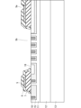
- ⁇ Modification> 22 is a schematic cross-sectional view showing the configuration of a semiconductor device 1 according to a modification of the first embodiment, and corresponds to FIG. 3.
- a protective film including a first protective film 18 covering the source electrode 3 and the gate line 2 and a second protective film 19 covering the first protective film 18 may be provided.
- the material of the first protective film 18 is preferably an insulating material or a semi-insulating material, such as SOG (Spin On Glass) or (Si x N y ).
- the material of the second protective film 19 is preferably an insulating material or a semi-insulating material, such as a polyimide film or a silicone resin.
- a source electrode 3 is provided in the center of the upper part of the semiconductor device 1, and a gate wiring 2 is provided so as to surround the source electrode 3.
- a gate pad 17 is provided between the center and the end of the semiconductor device 1 and is electrically connected to the gate wiring 2.
- the top view between the active region and the termination region in this second embodiment is similar to that in FIG. 2, with the SBD region 20 and the MOS region 22 arranged in a stripe pattern.
- FIG. 23 is a schematic cross-sectional view showing the configuration of the semiconductor device 1 according to the second embodiment, specifically, a schematic cross-sectional view of a portion taken along line a-a' in FIG. 2.
- the roughness of the surface of the gate electrode 6 that is connected to the first interlayer insulating film 7 is greater than the roughness of the surface of the gate electrode 6 that is connected to the second interlayer insulating film 5.
- the surface of the gate electrode 6 that is connected to the first interlayer insulating film 7 is the top surface, but it may be the side surface, or the top surface and the side surface.
- the flow chart showing the method for manufacturing the semiconductor device 1 according to the second embodiment is the same as that shown in Fig. 4.
- the SiC substrate 13 has n-type will be described in detail, but the SiC substrate may have p-type.
- the steps up to the step of forming a gate oxide film in the active region as the gate oxide film forming step S7 in Fig. 4 are the same as those in the first embodiment.
- a gate electrode 6 is formed on the upper surface of the first interlayer insulating film 7 by using photolithography and dry or wet etching techniques as shown in Fig. 12.
- the material of the conductive film that becomes the gate electrode 6 may be, for example, polycrystalline Si or poly-Si deposited by chemical vapor deposition or the like, or may be tungsten or tungsten silicide (WSi x ) when the semiconductor device 1 is to operate at a higher speed.
- photolithography is used appropriately to provide irregularities on the surface of the gate electrode 6 by dry etching using plasma containing fluorine or chlorine, or wet etching using a chemical solution containing hydrofluoric acid and nitric acid. This makes the surface of the gate electrode 6 that is connected to the first interlayer insulating film 7 rougher than the surface of the gate electrode 6 that is connected to the second interlayer insulating film 5 that will be formed later.
- annealing can be performed at a temperature of 500 to 700°C, and only the gate electrode 6 can be locally heated by flash lamp annealing.
- polysilicon can be formed from amorphous silicon, and finer irregularities can be provided on the surface of the gate electrode 6 than those formed by the above-mentioned etching method.
- the second interlayer insulating film formation process S9 an insulating film that will become the second interlayer insulating film 5 is formed using the CVD method, and then the insulating film is patterned using photolithography and dry or wet etching techniques. As a result, as shown in FIG. 25, the second interlayer insulating film 5 is formed, which covers the gate electrode 6 and the first interlayer insulating film 7 and has gate contact holes 5a and 5b. In this embodiment 1, the gate oxide film 8 becomes part of the second interlayer insulating film 5.
- the material of the second interlayer insulating film 5 is, for example, TEOS (tetra ethoxy silane) and BPSG (Boro-Phospho Silicate Glass).
- the contact region 9 is, for example, a nickel silicide layer formed by forming a metal film mainly composed of Ni (nickel) in an opening of a photoresist or the like by sputtering, and then performing a heat treatment at a temperature in the range of 600°C to 1100°C.
- a barrier metal layer 4 made of titanium or a titanium compound such as titanium nitride (TiN) is formed.
- a film of aluminum, an aluminum alloy made of aluminum and silicon, or nickel is formed to form the gate wiring 2 and the source electrode 3.
- the connection between the gate electrode 6 and the second interlayer insulating film 5 is strengthened by the fine irregularities on the surface of the gate electrode 6.
- the SiC substrate thinning process S12 and the drain electrode formation process S13 are performed to complete the semiconductor device 1 shown in FIG. 23.
- the surface roughness of the gate electrode 6 connected to the first interlayer insulating film 7 is greater than the surface roughness of the gate electrode 6 connected to the second interlayer insulating film 5.
- This configuration can increase the contact area between the gate electrode 6 and the second interlayer insulating film 5. This makes it possible to suppress peeling of the gate electrode 6 from the second interlayer insulating film 5 against external forces from various materials such as the mold resin 35 surrounding the gate electrode 6 of the semiconductor device 1, which are generated by the temperature difference between when heat is generated and when heat is not generated in the termination region. This makes it possible to further increase the reliability of the semiconductor device 1.
- ⁇ Modification> 27 is a schematic cross-sectional view showing the configuration of a semiconductor device 1 according to a modification of the second embodiment, and corresponds to FIG. 3.
- a protective film including a first protective film 18 covering the source electrode 3 and the gate wiring 2 and a second protective film 19 covering the first protective film 18 may be provided in the second embodiment as well.
- the material of the first protective film 18 is preferably an insulating material or a semi-insulating material, such as SOG (Spin On Glass) or a silicon nitride film (Si x N y ).
- the material of the second protective film 19 is preferably an insulating material or a semi-insulating material, such as a polyimide film or a silicone resin.
- a top view showing the configuration of a semiconductor device according to the third embodiment is similar to that of Fig. 1.
- a source electrode 3 is provided in the center of the upper part of the semiconductor device 1, and a gate wiring 2 is provided so as to surround the source electrode 3.
- a gate pad 17 is provided between the center and an end of the semiconductor device 1 and is electrically connected to the gate wiring 2.
- the top view between the active region and the termination region in this third embodiment is similar to that in FIG. 2, with the SBD region 20 and the MOS region 22 arranged in a stripe pattern.
- the schematic cross-sectional view of the portion along line a-a' in FIG. 2 is similar to that in FIG. 3.
- FIG. 28 is a schematic diagram showing the configuration of the termination region of the semiconductor device 1 according to the third embodiment.
- t gate1 which is the thickness of the gate electrode 6
- t insu1 which is the thickness of the first interlayer insulating film
- t insu1 which is the thickness of the first interlayer insulating film 7 is larger than t gate1 which is the thickness of the gate electrode 6. This will be described in detail later.
- the semiconductor device according to the third embodiment is manufactured, for example, according to the flow chart shown in Fig. 4.
- the steps of the third embodiment are generally the same as those of the first embodiment, and therefore a detailed description thereof will be omitted.
- the third embodiment when an insulating film to become the first interlayer insulating film 7 is formed by CVD in the first interlayer insulating film forming step S6, the first interlayer insulating film 7 is formed to be thicker than the gate electrode 6 in the subsequent gate electrode forming step S8.
- a current flows through the diode during a freewheeling operation.
- the semiconductor device 1 in which the BD region and the SBD region for passing a current during such a freewheeling operation are provided in the termination region heat is generated in the termination region of the semiconductor device 1.
- the temperature difference between when heat is being generated and when heat is not being generated in the termination region causes thermal stress in the gate electrode 6 and the second interlayer insulating film 5 that covers it due to the difference in the linear expansion coefficients of the various materials of the gate electrode 6, the second interlayer insulating film 5 that covers it, and the source electrode 3 and mold resin 35 that surround it.
- This stress causes an external force to be applied to the gate electrode 6 through the second interlayer insulating film 5, deteriorating the gate electrode 6 and causing a malfunction in the semiconductor device 1.
- t insu1 which is the thickness of the first interlayer insulating film 7 is made thicker than t gate1 which is the thickness of the gate electrode 6.
- ⁇ Fourth embodiment> 29 is a top view showing the configuration of a semiconductor device according to the fourth embodiment.
- a source electrode 3 is provided in the center of the upper part of the semiconductor device 1, and a gate wiring 2 is provided so as to surround the source electrode 3.
- a gate pad 17 is provided between the center and the end of the semiconductor device 1 and is electrically connected to the gate wiring 2.
- a protective insulating film 26 is provided to cover a part of the source electrode 3 provided in the upper part of the semiconductor device 1 and the gate wiring 2.
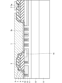
- FIG. 30 is a schematic cross-sectional view showing the configuration of the semiconductor device 1 according to the fourth embodiment, specifically, a schematic cross-sectional view of a portion taken along line a-a' in FIG. 2.
- the thickness of the portion of the protective insulating film 26 that is not above the gate electrode 6 but above the source electrode 3 is thicker than the thickness of the portion of the protective insulating film 26 that is above both the gate electrode 6 and the source electrode 3.
- ⁇ Production Method> 31 is a flowchart showing a method for manufacturing the semiconductor device 1 according to the fourth embodiment.
- the SiC substrate 13 has n-type will be described in detail, but the SiC substrate may have p-type.
- the steps of the fourth embodiment are the same as those of the first embodiment up to the contact region forming step S10, that is, up to the step of forming the contact region 9 in FIG.
- a barrier metal layer 4 made of titanium or a titanium compound such as titanium nitride (TiN) is formed.
- LPCVD Low Pressure Chemical Vapor Deposition
- PECVD Pullasma-Enhanced Chemical Vapor Deposition
- either aluminum or an aluminum alloy made of aluminum and silicon is deposited at a high temperature of 250 to 500°C, more preferably 350 to 450°C, using PVD (Physical Vapor Deposition) technology to form the gate wiring 2 and source electrode 3 as shown in Figure 33.
- PVD Physical Vapor Deposition
- sputtering is used as the PVD technology, for example.
- a surface protective film S11A a polyimide film or silicone resin is formed using lithography and screen printing techniques, and this is patterned to form the protective insulating film 26 in FIG. 30. Thereafter, as in the first embodiment, the thinning process S12 of the SiC substrate and the drain electrode forming process S13 are performed to complete the semiconductor device 1 shown in FIG. 30.
- a current flows through the diode during a freewheeling operation.
- the semiconductor device 1 in which the BD region and the SBD region for passing a current during such a freewheeling operation are provided in the termination region heat is generated in the termination region of the semiconductor device 1.
- the temperature difference between when heat is being generated and when heat is not being generated in the termination region causes thermal stress in the gate electrode 6 and the second interlayer insulating film 5 that covers it due to the difference in the linear expansion coefficients of the various materials of the gate electrode 6, the second interlayer insulating film 5 that covers it, and the source electrode 3 and mold resin 35 that surround it.
- This stress causes an external force to be applied to the gate electrode 6 through the second interlayer insulating film 5, deteriorating the gate electrode 6 and causing a malfunction in the semiconductor device 1.
- the thickness t pass1 of the protective insulating film 26 at a portion that is not above the gate electrode 6 but above the source electrode 3 is greater than the thickness t pass2 of the protective insulating film 26 at a portion that is above both the gate electrode 6 and the source electrode 3.
- the semiconductor device 1 according to the first to fourth embodiments is applied to a power conversion device.
- the semiconductor device 1 is, for example, a silicon carbide semiconductor device.
- the present disclosure is not limited to a specific power conversion device, hereinafter, a detailed description will be given of a case where the power conversion device according to the fifth embodiment is applied to a three-phase inverter.
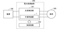
- FIG. 35 is a block diagram showing a schematic configuration of a power conversion system to which the power conversion device 200 according to the fifth embodiment is applied.
- This power conversion system is composed of a power source 100, a power conversion device 200, and a load 300.
- the power supply 100 is a DC power supply, and supplies DC power to the power conversion device 200.
- the power supply 100 can be configured from a variety of sources, for example, a DC system, a solar cell, or a storage battery, or it may be configured from a rectifier circuit or an AC/DC converter connected to an AC system.
- the power supply 100 may also be configured from a DC/DC converter that converts the DC power output from the DC system into a predetermined power.
- the power conversion device 200 is a three-phase inverter connected between the power source 100 and the load 300.
- the power conversion device 200 converts the DC power supplied from the power source 100 into AC power and supplies it to the load 300.
- the power conversion device 200 includes a main conversion circuit 201 and a control circuit 203.
- the main conversion circuit 201 converts the input DC power into AC power and outputs the AC power.
- the control circuit 203 outputs a control signal for controlling the main conversion circuit 201 to the main conversion circuit 201.
- the load 300 is a three-phase motor that is driven by AC power supplied from the power conversion device 200.
- the load 300 is not limited to a specific use, but is a motor mounted on various electrical devices, and is used, for example, as a motor for a hybrid vehicle, an electric vehicle, a railroad car, an elevator, or an air conditioning device.
- the power conversion device 200 will be described in detail below.
- the main conversion circuit 201 includes switching elements and freewheel diodes (not shown). By switching the switching elements, the main conversion circuit 201 converts the DC power supplied from the power source 100 into AC power and supplies it to the load 300.
- the main conversion circuit 201 There are various specific circuit configurations of the main conversion circuit 201, but the main conversion circuit 201 according to the present embodiment 5 is a two-level three-phase full bridge circuit that can be configured with six switching elements and six freewheel diodes connected in reverse parallel to each switching element.
- the semiconductor device 1 according to any of the above-mentioned embodiments 1 to 4 and their modifications is applied as at least one of the switching elements and freewheel diodes of the main conversion circuit 201.
- the six switching elements are connected in series with two switching elements to form upper and lower arms, and each upper and lower arm forms each phase (U phase, V phase, W phase) of the full bridge circuit.
- the output terminals of each upper and lower arm i.e., the three output terminals of the main conversion circuit 201, are connected to the load 300.
- the main conversion circuit 201 also includes a drive circuit (not shown) that drives each switching element.
- the drive circuit generates drive signals that drive the switching elements of the main conversion circuit 201 and supplies them to the control electrodes of the switching elements of the main conversion circuit 201. Specifically, in accordance with a control signal from a control circuit 203 (described later), a drive signal that switches the switching element to an on state and a drive signal that switches the switching element to an off state are output to the control electrodes of each switching element.
- the drive signal When maintaining a switching element in an on state, the drive signal is a voltage signal (on signal) that is greater than the threshold voltage of the switching element, and when maintaining a switching element in an off state, the drive signal is a voltage signal (off signal) that is less than the threshold voltage of the switching element.
- the control circuit 203 controls the switching elements of the main conversion circuit 201 so that the desired power is supplied to the load 300. Specifically, the control circuit 203 calculates the time (on time) that each switching element of the main conversion circuit 201 should be in the on state based on the power to be supplied to the load 300.
- the main conversion circuit 201 can be controlled by pulse width modulation (PWM) control, which modulates the on time of the switching elements according to the voltage to be output.
- PWM pulse width modulation
- the control circuit 203 outputs a control command (control signal) to the drive circuit provided in the main conversion circuit 201 so that at each point in time, an on signal is output to the switching element that should be in the on state, and an off signal is output to the switching element that should be in the off state.
- the drive circuit outputs an on signal or an off signal as a drive signal to the control electrode of each switching element according to this control signal.
- the manufacturing method of the power conversion device 200 has the following steps.
- the semiconductor device 1 is manufactured by the manufacturing method described in the above-mentioned embodiment or its modified example.
- a main conversion circuit 201 having this semiconductor device 1 is formed.
- a control circuit 203 is formed. This results in the power conversion device 200.
- the drain electrode 14 of the semiconductor device 1 is bonded onto the mounting substrate, and the source electrode 3 of the semiconductor device 1 is bonded to the mounting substrate via a wire.
- the above-mentioned semiconductor device 1 is used as at least one of the semiconductor devices constituting the main conversion circuit 201. This makes it possible to suppress unexpected adverse effects on the assembly of the semiconductor device 1, while suppressing malfunctions of the semiconductor device 1 caused by stress from peripheral components during switching operations. This increases the reliability of the main conversion circuit 201. Thus, the reliability of the power conversion device 200 can be increased.
- the present disclosure is not limited to this and can be applied to various power conversion devices.
- the power conversion device is a two-level power conversion device, but it may be a multi-level power conversion device such as a three-level power conversion device.
- the present disclosure when supplying power to a single-phase load, the present disclosure may be applied to a single-phase inverter.
- the present disclosure when supplying power to a DC load, the present disclosure may also be applied to a DC/DC converter or an AC/DC converter.
- the power conversion device to which this disclosure is applied is not limited to the case where the load described above is an electric motor, but can also be used, for example, as a power supply device for an electric discharge machine, a laser processing machine, an induction heating cooker, or a non-contact power supply system, and can also be used as a power conditioner for a solar power generation system or a power storage system, etc.
- a thickness of the protective insulating film is greater than a thickness of a portion of the protective insulating film that is not above the first electrode but is above the second electrode, the thickness of the protective insulating film being greater than a thickness of a portion of the protective insulating film that is above both the first electrode and the second electrode.
Landscapes
- Electrodes Of Semiconductors (AREA)
- Internal Circuitry In Semiconductor Integrated Circuit Devices (AREA)
Priority Applications (2)
| Application Number | Priority Date | Filing Date | Title |
|---|---|---|---|
| JP2025513857A JPWO2024214501A1 (https=) | 2023-04-12 | 2024-03-19 | |
| CN202480021354.6A CN120958969A (zh) | 2023-04-12 | 2024-03-19 | 半导体装置以及电力转换装置 |
Applications Claiming Priority (2)
| Application Number | Priority Date | Filing Date | Title |
|---|---|---|---|
| JP2023-064654 | 2023-04-12 | ||
| JP2023064654 | 2023-04-12 |
Publications (1)
| Publication Number | Publication Date |
|---|---|
| WO2024214501A1 true WO2024214501A1 (ja) | 2024-10-17 |
Family
ID=93059125
Family Applications (1)
| Application Number | Title | Priority Date | Filing Date |
|---|---|---|---|
| PCT/JP2024/010727 Ceased WO2024214501A1 (ja) | 2023-04-12 | 2024-03-19 | 半導体装置及び電力変換装置 |
Country Status (3)
| Country | Link |
|---|---|
| JP (1) | JPWO2024214501A1 (https=) |
| CN (1) | CN120958969A (https=) |
| WO (1) | WO2024214501A1 (https=) |
Citations (9)
| Publication number | Priority date | Publication date | Assignee | Title |
|---|---|---|---|---|
| JPH04125972A (ja) * | 1990-09-17 | 1992-04-27 | Fuji Electric Co Ltd | Mos型半導体素子の製造方法 |
| JPH0945705A (ja) * | 1995-08-02 | 1997-02-14 | Hitachi Ltd | 半導体装置 |
| JP2005051091A (ja) * | 2003-07-30 | 2005-02-24 | Nec Kansai Ltd | 縦型電界効果トランジスタ及びその製造方法 |
| JP2008112823A (ja) * | 2006-10-30 | 2008-05-15 | Denso Corp | 炭化珪素半導体装置の製造方法 |
| JP2009004676A (ja) * | 2007-06-25 | 2009-01-08 | Seiko Epson Corp | 半導体装置及びその製造方法 |
| JP2010010215A (ja) * | 2008-06-24 | 2010-01-14 | Oki Semiconductor Co Ltd | 半導体装置の製造方法 |
| JP2011018877A (ja) * | 2009-06-09 | 2011-01-27 | Toshiba Corp | 電力用半導体素子 |
| JP2017139292A (ja) * | 2016-02-02 | 2017-08-10 | 富士電機株式会社 | 半導体装置及びその製造方法 |
| JP2023002835A (ja) * | 2018-04-27 | 2023-01-10 | 三菱電機株式会社 | 半導体装置および電力変換装置 |
-
2024
- 2024-03-19 WO PCT/JP2024/010727 patent/WO2024214501A1/ja not_active Ceased
- 2024-03-19 JP JP2025513857A patent/JPWO2024214501A1/ja active Pending
- 2024-03-19 CN CN202480021354.6A patent/CN120958969A/zh active Pending
Patent Citations (9)
| Publication number | Priority date | Publication date | Assignee | Title |
|---|---|---|---|---|
| JPH04125972A (ja) * | 1990-09-17 | 1992-04-27 | Fuji Electric Co Ltd | Mos型半導体素子の製造方法 |
| JPH0945705A (ja) * | 1995-08-02 | 1997-02-14 | Hitachi Ltd | 半導体装置 |
| JP2005051091A (ja) * | 2003-07-30 | 2005-02-24 | Nec Kansai Ltd | 縦型電界効果トランジスタ及びその製造方法 |
| JP2008112823A (ja) * | 2006-10-30 | 2008-05-15 | Denso Corp | 炭化珪素半導体装置の製造方法 |
| JP2009004676A (ja) * | 2007-06-25 | 2009-01-08 | Seiko Epson Corp | 半導体装置及びその製造方法 |
| JP2010010215A (ja) * | 2008-06-24 | 2010-01-14 | Oki Semiconductor Co Ltd | 半導体装置の製造方法 |
| JP2011018877A (ja) * | 2009-06-09 | 2011-01-27 | Toshiba Corp | 電力用半導体素子 |
| JP2017139292A (ja) * | 2016-02-02 | 2017-08-10 | 富士電機株式会社 | 半導体装置及びその製造方法 |
| JP2023002835A (ja) * | 2018-04-27 | 2023-01-10 | 三菱電機株式会社 | 半導体装置および電力変換装置 |
Also Published As
| Publication number | Publication date |
|---|---|
| JPWO2024214501A1 (https=) | 2024-10-17 |
| CN120958969A (zh) | 2025-11-14 |
Similar Documents
| Publication | Publication Date | Title |
|---|---|---|
| US11984492B2 (en) | Silicon carbide semiconductor device, power converter, and method of manufacturing silicon carbide semiconductor device | |
| CN108886055B (zh) | 半导体装置及其制造方法、电力变换装置 | |
| US11158704B2 (en) | Semiconductor device and power conversion device | |
| JP7370476B2 (ja) | 炭化珪素半導体装置の製造方法、炭化珪素半導体装置および電力変換装置 | |
| JP7047981B1 (ja) | 炭化珪素半導体装置および電力変換装置 | |
| JP7229428B2 (ja) | 電力用半導体装置、電力用半導体装置の製造方法および電力変換装置 | |
| JP7664872B2 (ja) | 半導体装置、電力変換装置および半導体装置の製造方法 | |
| JP7275407B1 (ja) | 炭化珪素半導体装置、電力変換装置および炭化珪素半導体装置の製造方法 | |
| JP7062143B1 (ja) | 半導体装置及び電力変換装置 | |
| WO2024214501A1 (ja) | 半導体装置及び電力変換装置 | |
| JP7595771B2 (ja) | 半導体装置、電力変換装置および半導体装置の製造方法 | |
| US12464767B2 (en) | Semiconductor device and power conversion device | |
| WO2023048122A1 (ja) | 半導体装置および電力変換装置 | |
| JP7785159B2 (ja) | 半導体装置及び電力変換装置 | |
| WO2024214634A1 (ja) | 半導体装置及び電力変換装置 | |
| JP7607834B1 (ja) | 半導体装置、半導体装置の製造方法、及び、電力変換装置 | |
| JP7529139B2 (ja) | 炭化珪素半導体装置とその製造方法、および、電力変換装置 | |
| JP7584657B2 (ja) | 炭化珪素半導体装置および炭化珪素半導体装置を用いた電力変換装置 | |
| JP7573747B2 (ja) | 炭化珪素半導体装置および炭化珪素半導体装置を用いた電力変換装置 | |
| JP2024123834A (ja) | 炭化珪素半導体装置及び電力変換装置 | |
| JP6511125B2 (ja) | 半導体装置の製造方法 | |
| WO2025191758A1 (ja) | 半導体装置、電力変換装置および半導体装置の製造方法 | |
| JP2025008136A (ja) | 半導体装置、半導体装置の製造方法、及び、電力変換装置 | |
| WO2024257633A1 (ja) | 半導体装置、電力変換装置、半導体装置の製造方法 | |
| WO2024237071A1 (ja) | 半導体装置、電力変換装置、半導体装置の製造方法、および、電力変換装置の製造方法 |
Legal Events
| Date | Code | Title | Description |
|---|---|---|---|
| 121 | Ep: the epo has been informed by wipo that ep was designated in this application |
Ref document number: 24788531 Country of ref document: EP Kind code of ref document: A1 |
|
| WWE | Wipo information: entry into national phase |
Ref document number: 2025513857 Country of ref document: JP |
|
| NENP | Non-entry into the national phase |
Ref country code: DE |
|
| 122 | Ep: pct application non-entry in european phase |
Ref document number: 24788531 Country of ref document: EP Kind code of ref document: A1 |