WO2024203403A1 - 高分子分散型液晶フィルムおよびその使用方法 - Google Patents
高分子分散型液晶フィルムおよびその使用方法 Download PDFInfo
- Publication number
- WO2024203403A1 WO2024203403A1 PCT/JP2024/010077 JP2024010077W WO2024203403A1 WO 2024203403 A1 WO2024203403 A1 WO 2024203403A1 JP 2024010077 W JP2024010077 W JP 2024010077W WO 2024203403 A1 WO2024203403 A1 WO 2024203403A1
- Authority
- WO
- WIPO (PCT)
- Prior art keywords
- liquid crystal
- crystal compound
- polymer
- photoreactive
- polymer dispersed
- Prior art date
- Legal status (The legal status is an assumption and is not a legal conclusion. Google has not performed a legal analysis and makes no representation as to the accuracy of the status listed.)
- Ceased
Links
Images
Classifications
-
- G—PHYSICS
- G02—OPTICS
- G02F—OPTICAL DEVICES OR ARRANGEMENTS FOR THE CONTROL OF LIGHT BY MODIFICATION OF THE OPTICAL PROPERTIES OF THE MEDIA OF THE ELEMENTS INVOLVED THEREIN; NON-LINEAR OPTICS; FREQUENCY-CHANGING OF LIGHT; OPTICAL LOGIC ELEMENTS; OPTICAL ANALOGUE/DIGITAL CONVERTERS
- G02F1/00—Devices or arrangements for the control of the intensity, colour, phase, polarisation or direction of light arriving from an independent light source, e.g. switching, gating or modulating; Non-linear optics
- G02F1/01—Devices or arrangements for the control of the intensity, colour, phase, polarisation or direction of light arriving from an independent light source, e.g. switching, gating or modulating; Non-linear optics for the control of the intensity, phase, polarisation or colour
- G02F1/13—Devices or arrangements for the control of the intensity, colour, phase, polarisation or direction of light arriving from an independent light source, e.g. switching, gating or modulating; Non-linear optics for the control of the intensity, phase, polarisation or colour based on liquid crystals, e.g. single liquid crystal display cells
- G02F1/133—Constructional arrangements; Operation of liquid crystal cells; Circuit arrangements
- G02F1/1333—Constructional arrangements; Manufacturing methods
- G02F1/1334—Constructional arrangements; Manufacturing methods based on polymer dispersed liquid crystals, e.g. microencapsulated liquid crystals
-
- G—PHYSICS
- G02—OPTICS
- G02B—OPTICAL ELEMENTS, SYSTEMS OR APPARATUS
- G02B5/00—Optical elements other than lenses
- G02B5/30—Polarising elements
-
- G—PHYSICS
- G02—OPTICS
- G02F—OPTICAL DEVICES OR ARRANGEMENTS FOR THE CONTROL OF LIGHT BY MODIFICATION OF THE OPTICAL PROPERTIES OF THE MEDIA OF THE ELEMENTS INVOLVED THEREIN; NON-LINEAR OPTICS; FREQUENCY-CHANGING OF LIGHT; OPTICAL LOGIC ELEMENTS; OPTICAL ANALOGUE/DIGITAL CONVERTERS
- G02F1/00—Devices or arrangements for the control of the intensity, colour, phase, polarisation or direction of light arriving from an independent light source, e.g. switching, gating or modulating; Non-linear optics
- G02F1/01—Devices or arrangements for the control of the intensity, colour, phase, polarisation or direction of light arriving from an independent light source, e.g. switching, gating or modulating; Non-linear optics for the control of the intensity, phase, polarisation or colour
- G02F1/13—Devices or arrangements for the control of the intensity, colour, phase, polarisation or direction of light arriving from an independent light source, e.g. switching, gating or modulating; Non-linear optics for the control of the intensity, phase, polarisation or colour based on liquid crystals, e.g. single liquid crystal display cells
- G02F1/137—Devices or arrangements for the control of the intensity, colour, phase, polarisation or direction of light arriving from an independent light source, e.g. switching, gating or modulating; Non-linear optics for the control of the intensity, phase, polarisation or colour based on liquid crystals, e.g. single liquid crystal display cells characterised by the electro-optical or magneto-optical effect, e.g. field-induced phase transition, orientation effect, guest-host interaction or dynamic scattering
Definitions
- the present invention relates to a polymer dispersed liquid crystal film and a method for using the polymer dispersed liquid crystal film.
- a PDLC film having a polymer dispersed liquid crystal (hereinafter sometimes referred to as "PDLC") layer containing a polymer matrix and droplets of a liquid crystal compound between a pair of transparent electrode layers can change the degree of scattering of transmitted light in the PDLC layer depending on the amount of voltage applied.
- a PDLC film can switch between a light scattering state (scattering state) and a light transmitting state (transparent state) by switching between a voltage applied state and a voltage not applied state (Patent Document 1). Taking advantage of this function, the application of PDLC films to display bodies such as advertisements and guide boards, smart windows, etc. is being considered.
- the inventors have discovered that by producing a PDLC film using a polymerizable liquid crystal compound and polymerizing the polymerizable liquid crystal compound in the desired area, any design can be imparted to the PDLC film.
- This method makes it possible to obtain a PDLC film with a desired design, but once a design is applied, it is irreversible and cannot be changed to another design.
- the main objective of the present invention is to provide a PDLC film that allows the design to be changed once applied.
- a polymer dispersed liquid crystal film having a polymer dispersed liquid crystal layer including a polymer matrix and droplets dispersed in the polymer matrix and including a liquid crystal compound, the liquid crystal compound including a photoreactive liquid crystal compound having at least two reversible photodimerization functional groups.
- the liquid crystal compound may further include a non-reactive liquid crystal compound.
- the reversible photodimerization functional group may be selected from an anthracene group, a coumarin group, a cinnamic acid group, a stilbene group, and a thymine group.
- the photoreactive liquid crystal compound may include a photoreactive liquid crystal compound having three or more of the reversible photodimerization functional groups.
- the polymer dispersed liquid crystal film according to any one of the above [1] to [4] may further include a substrate with a transparent electrode layer disposed on both sides of the polymer dispersed liquid crystal layer.
- the amount of change in haze between a voltage applied state and a voltage not applied state may be changeable by a reversible photodimerization reaction of the photoreactive liquid crystal compound.
- the fixing step may be carried out again after the resetting step.
- the fixing step and the resetting step may be repeated.
- the region in which the liquid crystal polymer is produced in the second or subsequent fixing step may be different from the region in which the liquid crystal polymer is produced in the previous fixing step.
- a PDLC film in which a design once applied can be changed by using a photoreactive liquid crystal compound having a reversible photodimerization functional group as the liquid crystal compound.
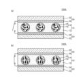
- FIG. 1 is a schematic cross-sectional view illustrating the configuration of a PDLC film in one embodiment of the present invention.
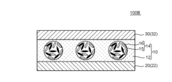
- FIG. 2 is a schematic cross-sectional view illustrating the configuration of a PDLC film according to another embodiment of the present invention.
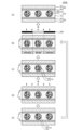
- FIG. 1 is a schematic diagram illustrating a method of using a PDLC film according to one embodiment of the present invention.
- FIG. 2 is a schematic diagram illustrating a method of using a PDLC film according to another embodiment of the present invention.
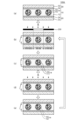
- FIG. 2 is a schematic diagram illustrating a method of using a PDLC film according to another embodiment of the present invention.
- 1 is a graph showing the change in haze when a voltage is applied to the PDLC film of the example.
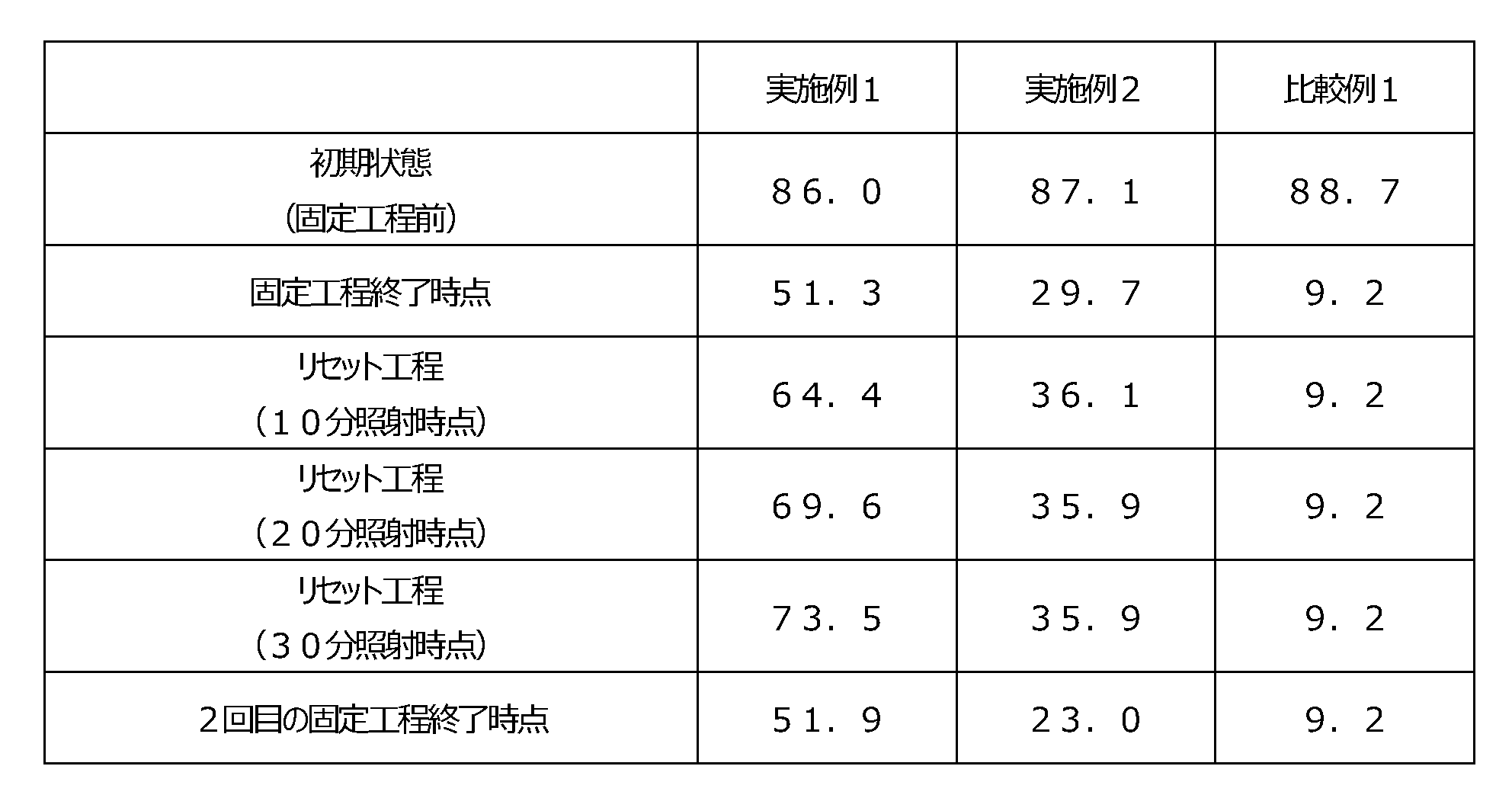
- 1 is a graph showing the haze of the PDLC film of the example in each process when no voltage is applied.
- a PDLC film having a PDLC layer including a polymer matrix and droplets containing a liquid crystal compound dispersed in the polymer matrix, the liquid crystal compound including a photoreactive liquid crystal compound having at least two reversible photodimerization functional groups.
- the photoreactive liquid crystal compound can be sequentially polymerized by a photodimerization reaction to generate a liquid crystal polymer.
- the liquid crystal polymer thus generated can be decomposed by a depolymerization reaction to generate a photoreactive liquid crystal compound (in other words, return to the photoreactive liquid crystal compound).
- the PDLC film according to the embodiment of the present invention can be applied with a desired design by arbitrarily forming regions with different haze or haze change amounts by utilizing the polymerization and depolymerization of the photoreactive liquid crystal compound, and furthermore, a design once applied can be changed.
- the PDLC film according to the embodiment of the present invention can be used, for example, as a rewritable light control film or a diffusion film.
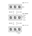
- FIG. 1 is a schematic cross-sectional view illustrating the configuration of a PDLC film in one embodiment of the present invention.
- the PDLC film 100A has a PDLC layer 10 including a polymer matrix 12 and droplets of a liquid crystal compound (hereinafter, sometimes referred to as "liquid crystal droplets") 14 dispersed in the polymer matrix 12.
- the liquid crystal droplets 14 include, as liquid crystal compounds, a photoreactive liquid crystal compound 15 having at least two reversible photodimerization functional groups and a non-reactive liquid crystal compound 16.
- the PDLC film 100A has a first substrate 20 on one side of the PDLC layer 10 and a second substrate 30 on the other side.
- the first substrate 20 and the second substrate 30 each have a substrate body 22, 32 and a transparent electrode layer 24, 34.
- the PDLC film 100A shown in FIG. 1 is in the normal mode. Specifically, as shown in FIG. 1(a), in the absence of applied voltage, the photoreactive liquid crystal compound 15 and the nonreactive liquid crystal compound 16 in the liquid crystal droplet 14 are not oriented, and scattering occurs due to the difference in refractive index between the polymer matrix 12 and the liquid crystal droplet 14, resulting in a scattered state. On the other hand, as shown in FIG. 1(a), in the absence of applied voltage, the photoreactive liquid crystal compound 15 and the nonreactive liquid crystal compound 16 in the liquid crystal droplet 14 are not oriented, and scattering occurs due to the difference in refractive index between the polymer matrix 12 and the liquid crystal droplet 14, resulting in a scattered state. On the other hand, as shown in FIG.
- the photoreactive liquid crystal compound 15 and the nonreactive liquid crystal compound 16 are oriented along the electric field direction, and the refractive index of the liquid crystal droplet 14 and the refractive index of the polymer matrix 12 are aligned, resulting in a transparent state with a lower haze than the scattered state.
- the PDLC film according to the embodiment of the present invention may be in the reverse mode, in which the PDLC film is in the scattered state in the presence of applied voltage and in the transparent state with a lower haze than the scattered state in the absence of applied voltage.
- the PDLC film 100A can change the amount of change in haze between the applied and unapplied voltage states, typically through the reversible photodimerization reaction of the photoreactive liquid crystal compound 15. Specifically, the amount of change in haze between the applied and unapplied voltage states can be reduced by sequentially polymerizing the photoreactive liquid crystal compound through photodimerization, and the amount of change in haze can be restored by depolymerizing the compound.
- the voltage applied to the PDLC film 100A in the voltage applied state is a voltage (operating voltage) that can operate the PDLC film 100A, and can be, for example, 5 V to 200 V, and preferably 10 V to 100 V.
- the "voltage applied state” means a state in which an operating voltage is applied to the PDLC film, and can be, for example, a state in which a voltage of 50 V is applied.
- the total thickness of the PDLC film 100A is, for example, 30 ⁇ m to 250 ⁇ m, preferably 50 ⁇ m to 150 ⁇ m.
- the PDLC layer 10 includes a polymer matrix 12 and liquid crystal droplets 14 dispersed in the polymer matrix 12.
- the liquid crystal droplets 14 include a photoreactive liquid crystal compound 15 and a non-reactive liquid crystal compound 16 as liquid crystal compounds.
- the liquid crystal droplets 14 include the non-reactive liquid crystal compound 16, but depending on the purpose, the liquid crystal droplets 14 may not include the non-reactive liquid crystal compound 16.
- the average particle diameter of the liquid crystal droplets 14 can be, for example, 0.3 ⁇ m to 9 ⁇ m, and preferably 0.4 ⁇ m to 8 ⁇ m. If the average particle diameter of the liquid crystal droplets is too small, the liquid crystal droplets are smaller than the wavelength of light, so the light passes through the liquid crystal droplets without being scattered, which can result in a problem of insufficient haze being obtained. If the average particle diameter of the liquid crystal droplets is too large, the liquid crystal droplets are too large compared to the wavelength of light, which can result in a problem of insufficient haze being obtained. Note that the above average particle diameter of the liquid crystal droplets is the volume average particle diameter of the liquid crystal droplets when viewed from a direction perpendicular to the main surface of the PDLC film.
- the particle size of the liquid crystal droplets preferably has a relatively narrow particle size distribution.
- the coefficient of variation (CV value) of the particle size of the liquid crystal droplets may be, for example, less than 0.4, preferably 0.35 or less, and more preferably 0.3 or less.
- the coefficient of variation can be calculated from the following formula.
- CV value standard deviation of particle size distribution of liquid crystal droplets / average particle size
- the polymer matrix 12 may be composed of any appropriate resin.
- the resin for forming the polymer matrix may be appropriately selected depending on the light transmittance, the refractive index of the liquid crystal compound, the adhesion to the substrate, etc. It is preferable that the resin for forming the polymer matrix has a refractive index close to that of the liquid crystal compound.
- the resin for forming the polymer matrix examples include thermoplastic resins such as urethane-based resins, polyvinyl alcohol-based resins, polyethylene-based resins, polypropylene-based resins, and acrylic-based resins.
- the thermoplastic resin is preferably a water-soluble resin or a water-dispersible resin.
- the resin for forming the polymer matrix include curable resins such as liquid crystal polymers, (meth)acrylic-based resins, silicone-based resins, epoxy-based resins, fluorine-based resins, polyester-based resins, and polyimide resins. Only one type of resin for forming the polymer matrix may be used, or two or more types may be used in combination.
- the photoreactive liquid crystal compound 15 a compound having at least two reversible photodimerization functional groups and exhibiting liquid crystallinity is used.
- the photoreactive liquid crystal compound can be sequentially polymerized by a photodimerization reaction to generate a liquid crystal polymer. Since the photodimerization reaction is reversible, the generated liquid crystal polymer can be decomposed (depolymerized) by irradiation with light and return to the photoreactive liquid crystal compound.
- liquid crystal polymers are typically non-liquid crystals. Therefore, in liquid crystal polymers, for example, the transition to a liquid crystal phase, glass phase, or crystalline phase due to temperature changes that is specific to liquid crystal compounds does not occur.
- the photoreactive liquid crystal compound is preferably a monomeric compound.
- the molecular weight of the photoreactive liquid crystal compound is, for example, 5000 or less, preferably 3000 or less, and may be 1500 or less.
- the dielectric anisotropy of the photoreactive liquid crystal compound may be positive or negative.
- the photoreactive liquid crystal compound may be, for example, a nematic, smectic, or cholesteric liquid crystal compound, and is preferably a nematic liquid crystal compound. Only one type of photoreactive liquid crystal compound may be used, or two or more types may be used in combination.
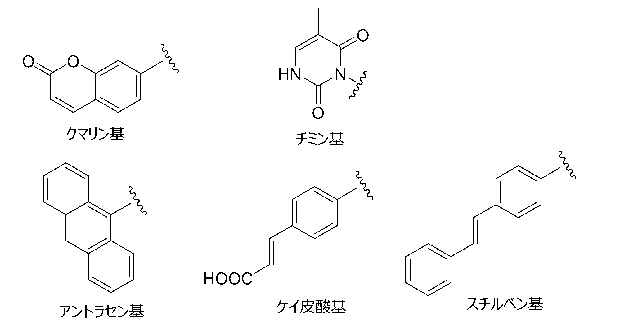
- any functional group capable of causing a reversible photodimerization reaction can be used, and preferred examples thereof include anthracene group, coumarin group, cinnamic acid group, stilbene group, thymine group, etc.
- the anthracene group, coumarin group, cinnamic acid group, stilbene group, and thymine group can have, for example, the structures shown below.
- the photoreactive liquid crystal compound may have two or more types of photodimerization functional groups.
- the photoreactive liquid crystal compound has a core (e.g., a mesogen portion) containing one or more ring structures and at least two reversible photodimerization functional groups arranged at the ends.
- the core and the photodimerization functional groups may be directly bonded to each other or may be bonded to each other via a spacer.
- the spacer may be, for example, a divalent linking group containing an alkylene group having 1 to 8 carbon atoms, an ether bond, an ester bond, an amide bond, or the like.
- the spacer may be -O-(C1-C8 alkylene)-O- or -C(O)-O-(C1-C8 alkylene)-O-.
- the number of photodimerization functional groups possessed by the photoreactive liquid crystal compound may be 2 or more, for example, 2 to 4, and preferably 2 or 3.
- a photoreactive liquid crystal compound having three or more photodimerization functional groups can generate a liquid crystal polymer having a network structure by crosslinking, and therefore, when used in combination with a nonreactive liquid crystal compound, the orientation of the nonreactive liquid crystal compound can be more suitably maintained.
- a photoreactive liquid crystal compound having three or more photodimerization functional groups can be used in a ratio of, for example, 10% by weight to 100% by weight, preferably 30% by weight to 100% by weight, based on the total amount of the photoreactive liquid crystal compound.
- Specific examples of photoreactive liquid crystal compounds include the photoreactive liquid crystal monomers described in JP-A-2008-260846.
- Photoreactive liquid crystal compounds typically do not have polymerizable functional groups capable of chain polymerization such as radical polymerization or ionic polymerization.
- a liquid crystal compound that is substantially non-reactive with other liquid crystal compounds can be appropriately selected and used.
- the non-reactive liquid crystal compound preferably does not have a reactive functional group (e.g., a functional group capable of chain polymerization or sequential polymerization).
- the non-reactive liquid crystal compound can be, for example, a nematic type, a smectic type, or a cholesteric type liquid crystal compound. It is preferable to use a nematic type liquid crystal compound because it can achieve excellent transparency in the transparent state. Only one type of non-reactive liquid crystal compound may be used, or two or more types may be used in combination.
- Nematic liquid crystal compounds include biphenyl compounds, phenylbenzoate compounds, cyclohexylbenzene compounds, azoxybenzene compounds, azobenzene compounds, azomethine compounds, terphenyl compounds, biphenylbenzoate compounds, cyclohexylbiphenyl compounds, phenylpyridine compounds, cyclohexylpyrimidine compounds, cholesterol compounds, fluorine compounds, etc.
- the polymer matrix content in the PDLC layer is, for example, 30% to 70% by weight, preferably 35% to 65% by weight, and more preferably 40% to 60% by weight. If the polymer matrix content is within this range, it is possible to obtain effects such as a good dimming function at a moderate operating voltage, good mechanical strength, and prevention of liquid crystal leakage from the edges.
- the weight ratio (former:latter) of the content of the polymer matrix to the content of the liquid crystal compounds (photoreactive liquid crystal compounds and nonreactive liquid crystal compounds, if present) in the PDLC layer is, for example, 30:70 to 70:30, preferably 35:65 to 65:35, and more preferably 40:60 to 60:40.
- the content of the photoreactive liquid crystal compounds in the PDLC layer is, for example, 1% to 20% by weight, preferably 1.5% to 15% by weight, and more preferably 2% to 10% by weight.
- the weight ratio (former:latter) of the content of the photoreactive liquid crystal compound to the content of the non-reactive liquid crystal compound in the PDLC layer is, for example, 1:99 to 40:60, preferably 2:98 to 35:75, and more preferably 3:97 to 30:70.
- the total content of the polymer matrix and liquid crystal compounds (photoreactive liquid crystal compounds and nonreactive liquid crystal compounds, if present) in the PDLC layer can be, for example, 90% to 99.9% by weight, preferably 95% to 99.9% by weight.
- the PDLC layer may further contain any appropriate component, as necessary.
- optional components include surfactants, leveling agents, crosslinking agents, dispersion stabilizers, polymerization initiators, etc.
- the content of the optional components in the PDLC layer may be, for example, 0.1% to 10% by weight, preferably 0.1% to 5% by weight.
- the thickness of the PDLC layer is typically 2 ⁇ m to 40 ⁇ m, preferably 3 ⁇ m to 35 ⁇ m, and more preferably 4 ⁇ m to 30 ⁇ m.
- the first substrate 20 is a substrate with a transparent electrode layer, which has a substrate body 22 and a transparent electrode layer 24 provided on one side (the PDLC layer 10 side) of the substrate body 22.
- the first substrate 20 may have a hard coat layer on one or both sides of the substrate body 22, and may have a refractive index adjustment layer between the substrate body 22 and the transparent electrode layer 24, as necessary.
- the surface resistance of the first substrate is preferably 1 ⁇ / ⁇ to 1000 ⁇ / ⁇ , more preferably 5 ⁇ / ⁇ to 300 ⁇ / ⁇ , and even more preferably 10 ⁇ / ⁇ to 200 ⁇ / ⁇ .
- the haze value of the first substrate is preferably 20% or less, more preferably 10% or less, and even more preferably 0.1% to 10%.
- the total light transmittance of the first substrate is preferably 40% or more, more preferably 60% or more, and even more preferably 80% or more.
- the total light transmittance can be measured in accordance with JIS K 7361.
- the substrate body 22 may be formed using any suitable material.
- the substrate body is a polymer film mainly composed of a thermoplastic resin.
- thermoplastic resins include polyester resins; cycloolefin resins such as polynorbornene; acrylic resins; polycarbonate resins; and cellulose resins. Of these, polyester resins, cycloolefin resins, and acrylic resins are preferred. These resins are excellent in transparency, mechanical strength, thermal stability, and moisture shielding properties.
- the above thermoplastic resins may be used alone or in combination of two or more.
- optical films such as those used in polarizing plates, such as low retardation substrates, high retardation substrates, retardation plates, absorptive polarizing films, and polarized selective reflection films, can also be used as the substrate body.
- the thickness of the substrate body is preferably 200 ⁇ m or less, more preferably 3 ⁇ m to 100 ⁇ m, and even more preferably 5 ⁇ m to 70 ⁇ m. By making the thickness of the substrate body 200 ⁇ m or less, the PDLC layer can fully exhibit its functions.
- the total light transmittance of the substrate body is preferably 40% or more, more preferably 60% or more, and even more preferably 80% or more.
- the transparent electrode layer 24 may be formed using a metal oxide such as indium tin oxide (ITO), zinc oxide (ZnO), or tin oxide (SnO 2 ).
- the metal oxide may be an amorphous metal oxide or a crystallized metal oxide.
- the transparent electrode layer may also be formed by a metal nanowire such as silver nanowire (AgNW), a carbon nanotube (CNT), an organic conductive film, a metal layer, or a laminate thereof.
- a transparent electrode layer containing ITO is preferably formed.
- the transparent electrode layer containing ITO has excellent transparency.
- the transparent electrode layer may be patterned into a desired shape depending on the purpose.
- the total light transmittance of the transparent electrode layer is preferably 85% or more, more preferably 87% or more, and even more preferably 90% or more.
- a transparent electrode layer having a total light transmittance in this range a PDLC film having high light transmittance in the transparent state can be obtained.
- the thickness of the transparent electrode layer is, for example, 10 nm or more, and preferably 15 nm or more.
- the thickness of the transparent electrode layer is, for example, 50 nm or less, and preferably 35 nm or less, and more preferably 30 nm or less.
- the transparent electrode layer is provided on one side of the substrate body, for example, by sputtering. After forming the metal oxide layer by sputtering, it can be crystallized by annealing. Annealing is performed, for example, by heat treatment at 120°C to 300°C for 10 to 120 minutes.
- the refractive index adjustment layer and hard coat layer may have configurations that are well known in the art, so detailed descriptions of their configurations will be omitted.
- the second substrate 30 is typically a substrate with a transparent electrode layer having a substrate body 32 and a transparent electrode layer 34 provided on one side (the PDLC layer 10 side) of the substrate body 32.
- the second substrate 30 may have a hard coat layer on one or both sides of the substrate body 32 as required, and may also have a refractive index adjustment layer between the substrate body 32 and the transparent electrode layer 34.
- the surface resistance of the second substrate is preferably 1 ⁇ / ⁇ to 1000 ⁇ / ⁇ , more preferably 5 ⁇ / ⁇ to 300 ⁇ / ⁇ , and even more preferably 10 ⁇ / ⁇ to 200 ⁇ / ⁇ .
- the haze value of the second substrate is preferably 20% or less, more preferably 10% or less, and even more preferably 0.1% to 10%.
- the total light transmittance of the second substrate is preferably 40% or more, more preferably 60% or more, and even more preferably 80% or more.
- the same explanations as for the substrate body 22 and transparent electrode layer 24 in the first substrate 20 can be applied to the substrate body 32 and transparent electrode layer 34, respectively.
- the second substrate may have the same configuration as the first substrate, or may have a different configuration.
- the manufacturing method of the PDLC film includes preparing a coating liquid containing a resin for forming a polymer matrix, a liquid crystal compound (a photoreactive liquid crystal compound and a non-reactive liquid crystal compound when present), and a dispersion medium; applying the coating liquid to one side of a first substrate to form a coating layer; drying the coating layer to form a polymer matrix in the resin for forming a polymer matrix to obtain a PDLC layer; and laminating a second substrate on the PDLC layer.
- the coating liquid is preferably an emulsion coating liquid in which liquid crystal particles containing a liquid crystal compound are dispersed in a dispersion medium.
- a dispersion medium water or a mixed solvent of water and a water-miscible organic solvent can be preferably used.
- the water-miscible organic solvent C1-3 alcohol, acetone, DMSO, etc. can be mentioned.
- a method for producing a PDLC film includes preparing a coating liquid containing a curable resin for forming a polymer matrix, a liquid crystal compound (a photoreactive liquid crystal compound and a non-reactive liquid crystal compound, if present), and a polymerization initiator; applying the coating liquid to one side of a first substrate to form a coating layer; laminating a second substrate on the coating layer to form a laminate; and irradiating the laminate with active energy rays to polymerize the curable resin and form a polymer matrix, thereby obtaining a PDLC layer.
- the coating liquid is preferably in a homogeneous phase state, and the polymer matrix and the liquid crystal compound may be phase-separated with the polymerization of the curable resin.
- Ultraviolet rays are preferably used as the active energy rays.
- the coating liquid may be filled between the first substrate and the second substrate, which are laminated via a spacer, and then phase separation may be performed by irradiating with active energy rays.
- FIG. 2 is a schematic cross-sectional view illustrating the configuration of a PDLC film in another embodiment of the present invention.
- the PDLC film 100B has a PDLC layer 10 including a polymer matrix 12 and liquid crystal droplets 14 dispersed in the polymer matrix 12.
- the liquid crystal droplets 14 include a photoreactive liquid crystal compound 15 having at least two reversible photodimerization functional groups and a non-reactive liquid crystal compound 16 as liquid crystal compounds.
- the PDLC film 100B has a first substrate 20 on one side of the PDLC layer 10 and a second substrate 30 on the other side.
- the first substrate 20 and the second substrate 30 are composed of substrate bodies 22 and 32, respectively, and do not have a transparent electrode layer.
- the PDLC film 100B having such a configuration can be preferably used as, for example, a diffusion film.
- the same explanation as above can be applied to the PDLC layer 10 and the substrate bodies 22 and 32.
- the PDLC film 100B can be manufactured by a method similar to the method described in A-5.
- the method of using the PDLC film described in section A includes the steps of: The method includes a fixing step of producing a liquid crystal polymer by a photodimerization reaction of a photoreactive liquid crystal compound, and a reset step of producing the photoreactive liquid crystal compound by a depolymerization reaction of the liquid crystal polymer.
- the fixing step can be carried out again after the reset step.
- the fixing step and the reset step can be carried out repeatedly.
- the number of repetitions is not limited as long as the effect of the present invention can be obtained.
- the region in which the liquid crystal polymer is generated in the second or subsequent fixing steps can be different from the region in which the liquid crystal polymer was generated in the previous fixing step.
- the PDLC film described in Section A can be used as a rewritable PDLC film.
- the method of using the PDLC film according to one embodiment of the present invention will be specifically described with reference to FIG. 3.
- a PDLC film 100A is prepared, which has a PDLC layer 10 including a polymer matrix 12 and liquid crystal droplets 14 dispersed in the polymer matrix 12, and a first substrate 20 and a second substrate 30 disposed on either side of the PDLC layer 10, and the liquid crystal droplets 14 include a photoreactive liquid crystal compound 15 having at least two reversible photodimerization functional groups.
- the liquid crystal droplets 14 further include a non-reactive liquid crystal compound 16.
- the PDLC film 100A is irradiated with light to promote the photodimerization reaction of the photoreactive liquid crystal compound 15 (FIG. 3B).
- the photoreactive liquid crystal compound 15 is sequentially polymerized to generate a liquid crystal polymer 17 (FIG. 3C).
- light is irradiated through a photomask 200 having a predetermined pattern while a voltage is applied to the PDLC layer 10.
- the photoreactive liquid crystal compound 15 in the irradiated area can be polymerized in a state in which it is aligned in the electric field direction.
- the generated liquid crystal polymer 17 does not have liquid crystal properties and does not respond to the electric field.
- the liquid crystal polymer 17 is fixed in a state in which it is aligned in the thickness direction, and the nonreactive liquid crystal compound 16 in the same liquid crystal droplet 14 is subject to the alignment restriction by the liquid crystal polymer 17.
- the irradiated area is transparent with low haze in both the voltage application state and the non-voltage application state.
- the photodimerization reaction of the photoreactive liquid crystal compound 15 does not occur in the non-irradiated area, the liquid crystal polymer 17 is not generated, and the liquid crystal droplet 14 can change the refractive index depending on the voltage application state.
- the non-irradiated region is in a scattering state with high haze when no voltage is applied, and the haze is reduced by applying a voltage, so that the non-irradiated region becomes transparent. Therefore, according to the fixing process, a first region (irradiated region) and a second region (non-irradiated region) having different amounts of haze change between the applied and unapplied states can be formed in a desired pattern by using a photomask corresponding to the desired pattern. The amount of haze change in the first region between the applied and unapplied states is smaller than the amount of haze change in the second region.
- the light irradiation conditions in the fixing step may be any conditions that cause a photodimerization reaction of the photoreactive liquid crystal compound, and the irradiation conditions such as the wavelength, irradiation time, and irradiation temperature of the irradiation light may be appropriately set according to the type of the photoreactive liquid crystal compound.
- the peak wavelength of the irradiation light may be, for example, 315 nm to 400 nm, or, for example, 330 nm to 380 nm.
- the exposure dose may be, for example, 10 J/m 2 to 10,000 J/m 2 , or, for example, 100 J/m 2 to 5,000 J/m 2.
- the irradiation temperature may be, for example, -20°C to 80°C, or, for example, -20°C to 60°C.
- the PDLC film 100A is irradiated with light to promote the depolymerization reaction of the liquid crystal polymer 17 (FIG. 3(d)). This causes the liquid crystal polymer 17 to decompose, generating the photoreactive liquid crystal compound 15 (FIG. 3(e)).
- the entire surface of the PDLC film 100A is irradiated with light, but it may also be irradiated only to the irradiated area.
- the reset process can erase the pattern applied to the PDLC film 100A.
- the entire pattern is erased and reset to the original state, but it may also be in a state where part of the liquid crystal polymer is depolymerized and the pattern is relaxed (the haze difference of the pattern is reduced). Light irradiation may also be performed under a voltage application state.
- the light irradiation conditions in the resetting step may be any conditions that cause a depolymerization reaction of the liquid crystal polymer, and the irradiation conditions such as the wavelength, irradiation time, and irradiation temperature of the irradiation light may be appropriately set according to the type of the photoreactive liquid crystal compound.
- the peak wavelength of the irradiation light in the resetting step may be shorter than the peak wavelength of the irradiation light in the fixing step.
- the peak wavelength of the irradiation light may be, for example, 230 nm to 290 nm, or, for example, 240 nm to 290 nm.
- the exposure dose may be, for example, 10 J/m 2 to 10,000 J/m 2 , or, for example, 100 J/m 2 to 5,000 J/m 2.
- the irradiation temperature may be, for example, -20°C to 80°C, or, for example, -20°C to 60°C.
- the fixing process can be carried out again after the reset process.
- the PDLC film 100A after the reset process can be irradiated with light to promote the photodimerization reaction of the photoreactive liquid crystal compound 15. This causes the photoreactive liquid crystal compound 15 to polymerize sequentially, producing the liquid crystal polymer 17 (second fixing process).
- second fixing process by irradiating with light through a photomask with a different pattern from the photomask used in the first fixing process, a PDLC film having first and second regions in a different pattern from the pattern applied in the first fixing process can be obtained.
- the reset step can be performed again (second reset step).
- the second reset step can erase the pattern applied in the second fixing step.
- the pattern may be completely erased, or may be in a relaxed state (the haze difference of the pattern is reduced).
- the design (pattern) applied to the PDLC film 100A can be rewritten and changed to any desired design.
- the photodimerization reaction of the photoreactive liquid crystal compound is allowed to proceed in the fixing step with a voltage applied, but as shown in FIG. 4, the photodimerization reaction of the photoreactive liquid crystal compound may be allowed to proceed without a voltage being applied (FIG. 4(b)).
- the photoreactive liquid crystal compound 15 in the irradiated region is polymerized and fixed in a non-oriented state, and the photoreactive liquid crystal compound 15 in the non-irradiated region does not undergo a photodimerization reaction.
- the irradiated region (first region) is in a scattering state with high haze in both a voltage-applied state and a voltage-unapplied state
- the non-irradiated region (second region) is in a scattering state with high haze in a voltage-unapplied state
- the haze decreases with the application of a voltage to become transparent.
- the amount of change in haze between a voltage-applied state and a voltage-unapplied state in the first region (irradiated region) is smaller than the amount of change in haze in the second region (non-irradiated region).
- the above-mentioned method of using a PDLC film makes it possible to obtain a patterned PDLC film in which first and second regions, which have different amounts of haze change between a voltage applied state and a voltage not applied state, are formed in a predetermined pattern. Therefore, the method of using a PDLC film described in Section B can be a method of manufacturing a patterned PDLC film.
- the pattern applied to the patterned PDLC film according to the embodiment of the present invention can be reversibly changed.
- the method of using a PDLC film according to an embodiment of the present invention can also be applied to a PDLC film (diffusion film) 100B in which the substrate does not have a transparent electrode layer.
- a PDLC film diffusion film
- FIG. 5 by alternately repeating the above-mentioned fixing process and reset process on the PDLC film 100B, it is possible to form low haze regions and high haze regions of the PDLC film 100B in different patterns (patterns A and B in the illustrated example).
- the application of a voltage to the PDLC layer in the fixing process can be performed by arranging separately prepared electrodes on the surfaces of the first substrate and the second substrate and applying a voltage.
- the aperture size was set to 30 ⁇ m, and the volume average particle size was calculated by dividing the particle size into 256 equal intervals on a logarithmic basis from 0.6 ⁇ m to 18 ⁇ m, and the volume average particle size was calculated by taking the volume statistics for each particle size.
- (3) Average particle size of resin particles A few drops of the resin dispersion were added to 100 mL of water to prepare a measurement sample. Using a dynamic light scattering particle size distribution measurement device (manufactured by Microtrac, device name "Nanotrac 150”), the measurement sample was set in the measurement holder of the device, and the device monitor was used to confirm that the concentration was measurable, after which measurement was performed.
- Haze Measured using a haze meter (manufactured by Nippon Denshoku Industries Co., Ltd., product name "NDH4000”) in accordance with JIS K 7136.
- Example 1 (First Substrate and Second Substrate) An ITO layer was formed by sputtering on one surface of a PET substrate (thickness: 50 ⁇ m) to obtain a substrate having a structure of [substrate body/transparent electrode layer].
- the average particle size of the liquid crystal particles in the obtained liquid crystal emulsion was 3.5 ⁇ m.
- the PDLC films obtained in the above Examples and Comparative Examples were subjected to the following fixing step, and then to the following reset step 1 or 2.
- the PDLC films subjected to the reset step 2 were subjected to the following fixing step again.
- the PDLC films after the fixing step were not subjected to the reset step and were left at room temperature as control samples.
- [Fixation process] The PDLC film was irradiated with light (10 mW/m 2 ) having a peak wavelength of 365 nm for 10 minutes at a temperature of 25° C. with an AC voltage of 50 V applied to the PDLC layer.
- Figure 6 shows the change in haze when voltages of 0 V to 50 V are applied to the PDLC films of Examples 1 and 2 in the initial state (before the fixing process) and after the fixing process is completed.
- Table 1 shows the haze of the PDLC film that has been subjected to the reset process 2 with no voltage applied.
- the PDLC film of the present invention is suitable for use in a variety of applications, including advertising, signs, smart windows, etc.
- Reference Signs List 100 PDLC film 10 PDLC layer 12 Polymer matrix 14 Liquid crystal droplets 15 Photoreactive liquid crystal compound 16 Non-reactive liquid crystal compound 17 Liquid crystal polymer 20 First substrate 30 Second substrate
Landscapes
- Physics & Mathematics (AREA)
- Nonlinear Science (AREA)
- General Physics & Mathematics (AREA)
- Optics & Photonics (AREA)
- Chemical & Material Sciences (AREA)
- Crystallography & Structural Chemistry (AREA)
- Dispersion Chemistry (AREA)
- Mathematical Physics (AREA)
- Liquid Crystal (AREA)
- Liquid Crystal Substances (AREA)
- Compositions Of Macromolecular Compounds (AREA)
Abstract
Description
[2]上記[1]に記載の高分子分散型液晶フィルムにおいて、上記液晶化合物が、非反応性液晶化合物をさらに含んでよい。
[3]上記[1]または[2]に記載の高分子分散型液晶フィルムにおいて、上記可逆的な光二量化官能基が、アントラセン基、クマリン基、ケイ皮酸基、スチルベン基、およびチミン基から選択されてよい。
[4]上記[1]から[3]のいずれかに記載の高分子分散型液晶フィルムにおいて、上記光反応性液晶化合物が、上記可逆的な光二量化官能基を3つ以上有する光反応性液晶化合物を含んでよい。
[5]上記[1]から[4]のいずれかに記載の高分子分散型液晶フィルムにおいて、上記高分子分散型液晶層の両側に配置された透明電極層付基材をさらに有してよい。
[6]上記[1]から[5]のいずれかに記載の高分子分散型液晶フィルムにおいて、上記光反応性液晶化合物の可逆的な光二量化反応によって、電圧印加状態と無印加状態とにおけるヘイズの変化量を変化可能であってよい。
[7]本発明の別の局面によれば、上記[1]から[6]のいずれかに記載の高分子分散型液晶フィルムの使用方法であって、上記光反応性液晶化合物の光二量化反応により、液晶ポリマーを生成させる固定工程、および、上記液晶ポリマーの解重合反応により、上記光反応性液晶化合物を生成させるリセット工程、を含む、高分子分散型液晶フィルムの使用方法が提供される。
[8]上記[7]に記載の高分子分散型液晶フィルムの使用方法において、上記リセット工程の後に上記固定工程を再度行ってよい。
[9]上記[7]または[8]に記載の高分子分散型液晶フィルムの使用方法において、上記固定工程および上記リセット工程を繰り返してよい。
[10]上記[8]または[9]に記載の高分子分散型液晶フィルムの使用方法において、2回目以降の固定工程において上記液晶ポリマーを生成させる領域が、その前の固定工程において上記液晶ポリマーを生成させる領域と異なってよい。
本発明の1つの局面によれば、高分子マトリクスと、上記高分子マトリクス中に分散しており、液晶化合物を含む液滴と、を含むPDLC層を有し、上記液晶化合物が、少なくとも2つの可逆的な光二量化官能基を有する光反応性液晶化合物を含む、PDLCフィルムが提供される。上記光反応性液晶化合物は、光二量化反応により逐次重合して液晶ポリマーを生成することができる。また、これにより生成する液晶ポリマーは、解重合反応により分解して光反応性液晶化合物を生成する(換言すれば、光反応性液晶化合物に戻る)ことができる。これらの反応は可逆反応であることから、本発明の実施形態によるPDLCフィルムは、光反応性液晶化合物の重合と解重合とを利用してヘイズまたはヘイズの変化量が異なる領域を任意に形成して所望の意匠を施すことができ、さらには、一旦施された意匠を変更することができる。よって、本発明の実施形態によるPDLCフィルムは、例えば、書き換え可能な調光フィルムまたは拡散フィルムとして用いられ得る。
図1は、本発明の1つの実施形態におけるPDLCフィルムの構成を説明する概略断面図である。PDLCフィルム100Aは、高分子マトリクス12と高分子マトリクス12中に分散している液晶化合物の液滴(以下、「液晶液滴」と称する場合がある)14とを含むPDLC層10を有する。液晶液滴14は、液晶化合物として、少なくとも2つの可逆的な光二量化官能基を有する光反応性液晶化合物15および非反応性液晶化合物16を含んでいる。PDLCフィルム100Aは、PDLC層10の一方の側に第1基材20を有し、他方の側に第2基材30を有している。第1基材20および第2基材30はそれぞれ、基材本体22、32と透明電極層24、34とを有している。
PDLC層10は、高分子マトリクス12と高分子マトリクス12中に分散している液晶液滴14とを含む。図1に示す実施形態において液晶液滴14は、液晶化合物として、光反応性液晶化合物15および非反応性液晶化合物16を含んでいる。散乱状態におけるヘイズと透明状態におけるヘイズとの差が大きいPDLCフィルムを得る、動作電圧を低減する等の観点から、液晶液滴14が非反応性液晶化合物16を含むことが好ましいが、目的に応じて、液晶液滴14は、非反応性液晶化合物16を含まなくてもよい。
CV値=液晶液滴の粒子径分布の標準偏差/平均粒子径
第1基材20は、基材本体22とその一方の側(PDLC層10側)に設けられた透明電極層24とを有する透明電極層付基材である。第1基材20は、必要に応じて、基材本体22の片側または両側にハードコート層を有していてもよく、また、基材本体22と透明電極層24との間に屈折率調整層を有していてもよい。
第2基材30は、代表的には、基材本体32とその一方の側(PDLC層10側)に設けられた透明電極層34とを有する透明電極層付基材である。第2基材30は、必要に応じて、基材本体32の片側または両側にハードコート層を有していてもよく、また、基材本体32と透明電極層34との間に屈折率調整層を有していてもよい。
上記PDLCフィルムは任意の適切な製造方法で製造することができる。1つの実施形態において、PDLCフィルムの製造方法は、高分子マトリクス形成用樹脂、液晶化合物(光反応性液晶化合物および存在する場合の非反応性液晶化合物)、および分散媒を含む塗工液を調製すること;第1基材の片面に塗工液を塗工して塗工層を形成すること;塗工層を乾燥させて高分子マトリクス形成用樹脂に高分子マトリクスを形成させてPDLC層を得ること;および、PDLC層上に第2基材を積層することを含む。塗工液は、液晶化合物を含む液晶粒子が分散媒中に分散しているエマルション塗工液であることが好ましい。分散媒としては、水または水と水混和性有機溶媒との混合溶媒が好ましく用いられ得る。水混和性有機溶媒としては、C1-3アルコール、アセトン、DMSO等が挙げられる。
図2は、本発明の別の実施形態におけるPDLCフィルムの構成を説明する概略断面図である。PDLCフィルム100Bは、高分子マトリクス12と高分子マトリクス12中に分散している液晶液滴14とを含むPDLC層10を有する。液晶液滴14は、液晶化合物として、少なくとも2つの可逆的な光二量化官能基を有する光反応性液晶化合物15および非反応性液晶化合物16を含んでいる。PDLCフィルム100Bは、PDLC層10の一方の側に第1基材20を有し、他方の側に第2基材30を有している。第1基材20および第2基材30はそれぞれ、基材本体22、32から構成されており、透明電極層を有さない。このような構成を有するPDLCフィルム100Bは、例えば拡散フィルムとして好ましく用いられ得る。PDLC層10、基材本体22、32についてはそれぞれ、上記と同様の説明を適用することができる。PDLCフィルム100Bは、A-5項に記載の方法と同様の方法によって製造することができる。
本発明の別の局面によれば、A項に記載のPDLCフィルムの使用方法が提供される。本発明の実施形態によるPDLCフィルムの使用方法は、
光反応性液晶化合物の光二量化反応により、液晶ポリマーを生成させる固定工程、および
液晶ポリマーの解重合反応により、上記光反応性液晶化合物を生成させるリセット工程、を含む。
本発明の実施形態によるPDLCフィルムの使用方法においては、上記リセット工程の後に上記固定工程を再度行うことができる。また、上記固定工程およびリセット工程を繰り返し行ってもよい。繰り返し数は本発明の効果が得られる限りにおいて制限されない。2回目以降の固定工程において液晶ポリマーを生成させる領域は、その前の固定工程において液晶ポリマーを生成させた領域と異なっていてもよい。本発明の実施形態による使用方法によれば、A項に記載のPDLCフィルムを書き換え可能なPDLCフィルムとして使用することができる。以下、図3を参照しながら、本発明の1つの実施形態によるPDLCフィルムの使用方法を具体的に説明する。
デジタルマイクロメーター(アンリツ社製、製品名「KC-351C」)を用いて測定した。
(2)液晶エマルション中の液晶粒子の体積平均粒子径
電解質水溶液(コールター社製、「アイソトンII」)200mlに液晶エマルションを0.1重量%添加し、得られた混合液を測定試料としてマルチサイザー3(コールター社製、アパーチャーサイズ=20μm)を用いて、0.4μmから12μmまで対数基準で等間隔に256分割し離散化した粒子径ごとの体積の統計を取り、体積平均粒子径を算出した。なお、12μm以上の粒子が存在している場合は、アパーチャーサイズを30μmとし、0.6μmから18μmまで対数基準で等間隔に256分割し離散化した粒子径ごとの体積の統計を取ることで、体積平均粒子径を算出した。
(3)樹脂粒子の平均粒子径
100mLの水に樹脂分散体を数滴加えて測定試料を調製した。動的光散乱式粒子径分布測定装置(Microtrac社製、装置名「Nanotrac150」)を用いて、装置の測定ホルダに測定試料をセットし、測定可能な濃度であることを装置のモニタにて確認後に測定を行った。
(4)ヘイズ
ヘイズメーター(日本電色社製、製品名「NDH4000」)を用いて、JIS K 7136に基づいて測定した。
(第1基材および第2基材)
PET基材(厚み:50μm)の一方の面に、スパッタ法によりITO層を形成して、[基材本体/透明電極層]の構成を有する基材を得た。
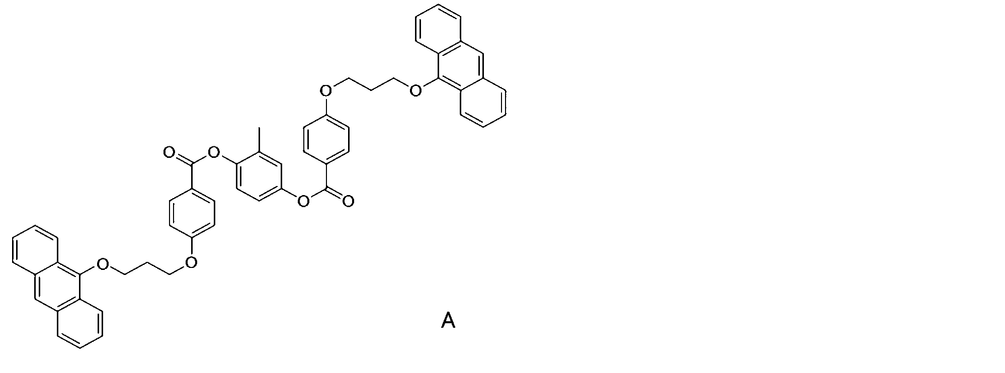
下記に示す光反応性液晶化合物A2.5部、非反応性液晶化合物(JNC社製、製品名「LX-153XX」、複屈折Δn=0.149)47部、純水49.5部、および界面活性剤(第一工業製薬社製、「ノイゲンET159」)1.0部を混合し、ホモジナイザーで処理することによって液晶エマルションを調製した。得られた液晶エマルション中の液晶粒子の平均粒子径は、3.5μmであった。
上記液晶エマルション47.6部、ポリエーテル系ポリウレタン樹脂水性分散体(DSM社製、商品名「NeoRezR967」、ポリマー平均粒子径:80nm、CV値=0.27、固形分:40wt%)32部、レベリング剤(DIC社製、製品名「F-444」)0.1部、架橋剤(トリス〔3-(2-メチルアジリジン-1-イル)プロピオン酸〕=プロピリジントリメチル)1部、および純水19.3部を混合することにより、エマルション塗工液を得た。
上記エマルション塗工液を、第1基材のITO層面に塗布し、40℃で乾燥させて、厚さ10μmのPDLC層を形成した。その後、ラミネーターを用いて0.4MPa/mのラミネート圧を適用しながら、上記PDLC層の上に第2基材を、ITO層がPDLC層に対向するように積層した。これにより、[第1基材/PDLC層/第2基材]の構成を有するPDLCフィルムを得た。
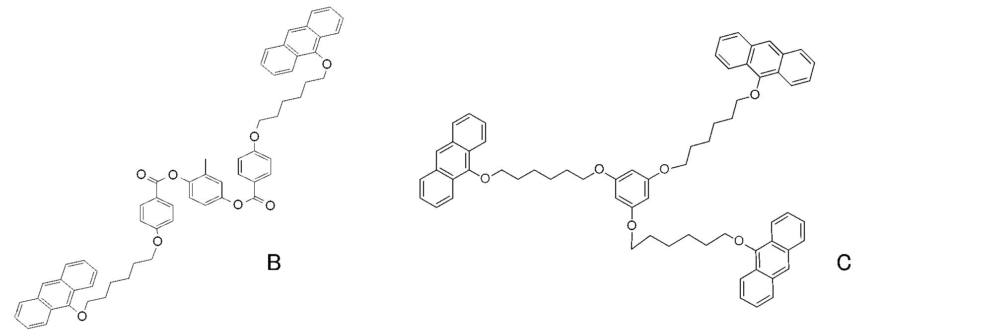
光反応性液晶化合物A2.5部の代わりに、下記に示す光反応性液晶化合物B1.25部および光反応性液晶化合物C1.25部を用いたこと以外は実施例1と同様にして、PDLCフィルムを得た。
非反応性液晶化合物(JNC社製、製品名「LX-153XX」、複屈折Δn=0.149)44.3部、重合性液晶化合物(BASF社製、製品名「PALIOCOLOR LC-242」)4.9部、光重合開始剤(IGM社製、製品名「OMNIRAD651」)0.3部、純水49.5部、および界面活性剤(第一工業製薬社製、「ノイゲンET159」)1.0部を混合し、ホモジナイザーで処理することによって液晶エマルションを調製した。得られた液晶エマルション中の液晶粒子の平均粒子径は、3.5μmであった。
上記のようにして得られた液晶エマルションを用いたこと以外は実施例1と同様にして、PDLCフィルムを得た。
[固定工程]
PDLCフィルムに対して、25℃の温度条件下、PDLC層に50Vの交流電圧を印加した状態で、ピーク波長が365nmである光(10mW/m2)を10分間照射した。
[リセット工程1]
固定工程後のPDLCフィルムに対して、ピーク波長が280nmである光(10mW/m2)を30分間照射した。
[リセット工程2]
固定工程後のPDLCフィルムに対して、ピーク波長が265nmである光(10mW/m2)を30分間照射した。
10 PDLC層
12 高分子マトリクス
14 液晶液滴
15 光反応性液晶化合物
16 非反応性液晶化合物
17 液晶ポリマー
20 第1基材
30 第2基材
Claims (10)
- 高分子マトリクスと、前記高分子マトリクス中に分散しており、液晶化合物を含む液滴と、を含む高分子分散型液晶層を有し、
前記液晶化合物が、少なくとも2つの可逆的な光二量化官能基を有する光反応性液晶化合物を含む、高分子分散型液晶フィルム。 - 前記液晶化合物が、非反応性液晶化合物をさらに含む、請求項1に記載の高分子分散型液晶フィルム。
- 前記可逆的な光二量化官能基が、アントラセン基、クマリン基、ケイ皮酸基、スチルベン基、およびチミン基から選択される、請求項1に記載の高分子分散型液晶フィルム。
- 前記光反応性液晶化合物が、前記可逆的な光二量化官能基を3つ以上有する光反応性液晶化合物を含む、請求項1に記載の高分子分散型液晶フィルム。
- 前記高分子分散型液晶層の両側に配置された透明電極層付基材をさらに有する、請求項1に記載の高分子分散型液晶フィルム。
- 前記光反応性液晶化合物の可逆的な光二量化反応によって、電圧印加状態と無印加状態とにおけるヘイズの変化量を変化可能である、請求項5に記載の高分子分散型液晶フィルム。
- 請求項1から6のいずれかに記載の高分子分散型液晶フィルムの使用方法であって、
前記光反応性液晶化合物の光二量化反応により、液晶ポリマーを生成させる固定工程、および
前記液晶ポリマーの解重合反応により、前記光反応性液晶化合物を生成させるリセット工程、を含む、高分子分散型液晶フィルムの使用方法。 - 前記リセット工程の後に前記固定工程を再度行う、請求項7に記載の高分子分散型液晶フィルムの使用方法。
- 前記固定工程および前記リセット工程を繰り返す、請求項7に記載の高分子分散型液晶フィルムの使用方法。
- 2回目以降の固定工程において前記液晶ポリマーを生成させる領域が、その前の固定工程において前記液晶ポリマーを生成させる領域と異なる、請求項8または9に記載の高分子分散型液晶フィルムの使用方法。
Priority Applications (3)
| Application Number | Priority Date | Filing Date | Title |
|---|---|---|---|
| KR1020257031666A KR20250162565A (ko) | 2023-03-30 | 2024-03-14 | 고분자 분산형 액정 필름 및 그의 사용 방법 |
| JP2025510476A JP7858914B2 (ja) | 2023-03-30 | 2024-03-14 | 高分子分散型液晶フィルムおよびその使用方法 |
| CN202480020834.0A CN120958357A (zh) | 2023-03-30 | 2024-03-14 | 高分子分散型液晶膜及其使用方法 |
Applications Claiming Priority (2)
| Application Number | Priority Date | Filing Date | Title |
|---|---|---|---|
| US202363493130P | 2023-03-30 | 2023-03-30 | |
| US63/493,130 | 2023-03-30 |
Publications (1)
| Publication Number | Publication Date |
|---|---|
| WO2024203403A1 true WO2024203403A1 (ja) | 2024-10-03 |
Family
ID=92905969
Family Applications (1)
| Application Number | Title | Priority Date | Filing Date |
|---|---|---|---|
| PCT/JP2024/010077 Ceased WO2024203403A1 (ja) | 2023-03-30 | 2024-03-14 | 高分子分散型液晶フィルムおよびその使用方法 |
Country Status (5)
| Country | Link |
|---|---|
| JP (1) | JP7858914B2 (ja) |
| KR (1) | KR20250162565A (ja) |
| CN (1) | CN120958357A (ja) |
| TW (1) | TW202445230A (ja) |
| WO (1) | WO2024203403A1 (ja) |
Citations (4)
| Publication number | Priority date | Publication date | Assignee | Title |
|---|---|---|---|---|
| JPH08240795A (ja) * | 1995-03-02 | 1996-09-17 | Nippon Telegr & Teleph Corp <Ntt> | 液晶素子及びその製造方法 |
| JPH1081083A (ja) * | 1996-09-06 | 1998-03-31 | Dainippon Printing Co Ltd | 情報表示媒体 |
| JPH10282489A (ja) * | 1997-04-04 | 1998-10-23 | Seiko Instr Inc | 反射型液晶表示装置 |
| JP2009256485A (ja) * | 2008-04-17 | 2009-11-05 | National Institute Of Advanced Industrial & Technology | ジアントラセンのアモルファスポリマーおよびそのポリマーを用いた光情報記録薄膜材料 |
Family Cites Families (7)
| Publication number | Priority date | Publication date | Assignee | Title |
|---|---|---|---|---|
| JPH0561023A (ja) * | 1991-06-21 | 1993-03-12 | Nec Corp | 液晶光学素子およびその製造方法 |
| JP2002189123A (ja) | 2000-12-19 | 2002-07-05 | Hitachi Chem Co Ltd | 調光材料、調光フィルム及び調光フィルムの製造方法 |
| JP5087762B2 (ja) | 2001-09-26 | 2012-12-05 | 独立行政法人産業技術総合研究所 | 光感応性液晶性組成物を内包するマイクロカプセル、およびこのマイクロカプセルを含む可逆記録材料 |
| JP4537718B2 (ja) * | 2004-01-22 | 2010-09-08 | 大日本印刷株式会社 | 液晶表示素子 |
| US8199086B2 (en) * | 2004-01-28 | 2012-06-12 | Kent Displays Incorporated | Stacked color photodisplay |
| JP5051520B2 (ja) | 2007-04-12 | 2012-10-17 | 独立行政法人産業技術総合研究所 | 光反応性液晶性モノマー及びそれを用いた主鎖型液晶ポリマーの製造方法 |
| US20170269400A1 (en) | 2016-03-17 | 2017-09-21 | Polytronix, Inc. | Polymeric Dispersed Liquid Crystal Light Shutter Device and System and Method for Forming the Same |
-
2024
- 2024-03-14 JP JP2025510476A patent/JP7858914B2/ja active Active
- 2024-03-14 KR KR1020257031666A patent/KR20250162565A/ko active Pending
- 2024-03-14 WO PCT/JP2024/010077 patent/WO2024203403A1/ja not_active Ceased
- 2024-03-14 CN CN202480020834.0A patent/CN120958357A/zh active Pending
- 2024-03-27 TW TW113111490A patent/TW202445230A/zh unknown
Patent Citations (4)
| Publication number | Priority date | Publication date | Assignee | Title |
|---|---|---|---|---|
| JPH08240795A (ja) * | 1995-03-02 | 1996-09-17 | Nippon Telegr & Teleph Corp <Ntt> | 液晶素子及びその製造方法 |
| JPH1081083A (ja) * | 1996-09-06 | 1998-03-31 | Dainippon Printing Co Ltd | 情報表示媒体 |
| JPH10282489A (ja) * | 1997-04-04 | 1998-10-23 | Seiko Instr Inc | 反射型液晶表示装置 |
| JP2009256485A (ja) * | 2008-04-17 | 2009-11-05 | National Institute Of Advanced Industrial & Technology | ジアントラセンのアモルファスポリマーおよびそのポリマーを用いた光情報記録薄膜材料 |
Non-Patent Citations (3)
Also Published As
| Publication number | Publication date |
|---|---|
| TW202445230A (zh) | 2024-11-16 |
| CN120958357A (zh) | 2025-11-14 |
| JP7858914B2 (ja) | 2026-05-14 |
| JPWO2024203403A1 (ja) | 2024-10-03 |
| KR20250162565A (ko) | 2025-11-18 |
Similar Documents
| Publication | Publication Date | Title |
|---|---|---|
| JP7120013B2 (ja) | 液晶デバイス用材料および液晶デバイス | |
| JP2002189123A (ja) | 調光材料、調光フィルム及び調光フィルムの製造方法 | |
| WO2017217430A1 (ja) | 液晶素子、液晶組成物並びに液晶素子を用いたスクリーン、ディスプレイ及び窓 | |
| CN102652167B (zh) | 液晶/高分子复合物、使用其的液晶显示装置、液晶/高分子复合物的制造方法 | |
| Yu et al. | Steric group-based polymer dispersed liquid crystal composite films with high contrast ratio, low driving voltage and small hysteresis | |
| CN106433690B (zh) | 液晶组合物以及液晶光学元件 | |
| JP7858914B2 (ja) | 高分子分散型液晶フィルムおよびその使用方法 | |
| JP2937590B2 (ja) | 液晶表示膜及びその作成方法 | |
| JP2002082364A (ja) | 調光材料、調光フィルム及び調光フィルムの製造方法 | |
| JPH01312527A (ja) | 液晶デバイス及びその製造方法 | |
| JP7496103B2 (ja) | 液晶組成物および温度応答性調光素子 | |
| JPH02309320A (ja) | 液晶調光・表示材料及びその製造方法 | |
| KR100321255B1 (ko) | 고분자분산형액정표시소자의제조방법 | |
| JP3383921B2 (ja) | 液晶デバイス | |
| KR20020093795A (ko) | 액정광셔터 | |
| JP3009496B2 (ja) | 液晶フィルム及び液晶構成体 | |
| JPH09329781A (ja) | 光散乱型液晶デバイス及びその製造方法 | |
| JP3269771B2 (ja) | 液晶表示装置の製造方法 | |
| JP2005352415A (ja) | 表示素子および表示装置 | |
| JPH03245121A (ja) | 液晶パネル | |
| JPH01252689A (ja) | 液晶デバイス | |
| JP2025169710A (ja) | 温度応答性調光素子及びその製造方法 | |
| JP2023046303A (ja) | 光拡散素子及びその製造方法並びに偏光フィルター | |
| JP2025059712A (ja) | 拡散フィルムおよび光拡散装置 | |
| JPH02310520A (ja) | 液晶調光・表示材料及びその製造方法 |
Legal Events
| Date | Code | Title | Description |
|---|---|---|---|
| 121 | Ep: the epo has been informed by wipo that ep was designated in this application |
Ref document number: 24779532 Country of ref document: EP Kind code of ref document: A1 |
|
| WWE | Wipo information: entry into national phase |
Ref document number: 2025510476 Country of ref document: JP |
|
| ENP | Entry into the national phase |
Ref document number: 1020257031666 Country of ref document: KR Free format text: ST27 STATUS EVENT CODE: A-0-1-A10-A15-NAP-PA0105 (AS PROVIDED BY THE NATIONAL OFFICE) |
|
| WWE | Wipo information: entry into national phase |
Ref document number: CN2024800208340 Country of ref document: CN |
|
| NENP | Non-entry into the national phase |
Ref country code: DE |
|
| 122 | Ep: pct application non-entry in european phase |
Ref document number: 24779532 Country of ref document: EP Kind code of ref document: A1 |