WO2024203117A1 - 高分子分散型液晶フィルム - Google Patents
高分子分散型液晶フィルム Download PDFInfo
- Publication number
- WO2024203117A1 WO2024203117A1 PCT/JP2024/008798 JP2024008798W WO2024203117A1 WO 2024203117 A1 WO2024203117 A1 WO 2024203117A1 JP 2024008798 W JP2024008798 W JP 2024008798W WO 2024203117 A1 WO2024203117 A1 WO 2024203117A1
- Authority
- WO
- WIPO (PCT)
- Prior art keywords
- liquid crystal
- less
- pdlc
- layer
- film
- Prior art date
- Legal status (The legal status is an assumption and is not a legal conclusion. Google has not performed a legal analysis and makes no representation as to the accuracy of the status listed.)
- Ceased
Links
Images
Classifications
-
- G—PHYSICS
- G02—OPTICS
- G02F—OPTICAL DEVICES OR ARRANGEMENTS FOR THE CONTROL OF LIGHT BY MODIFICATION OF THE OPTICAL PROPERTIES OF THE MEDIA OF THE ELEMENTS INVOLVED THEREIN; NON-LINEAR OPTICS; FREQUENCY-CHANGING OF LIGHT; OPTICAL LOGIC ELEMENTS; OPTICAL ANALOGUE/DIGITAL CONVERTERS
- G02F1/00—Devices or arrangements for the control of the intensity, colour, phase, polarisation or direction of light arriving from an independent light source, e.g. switching, gating or modulating; Non-linear optics
- G02F1/01—Devices or arrangements for the control of the intensity, colour, phase, polarisation or direction of light arriving from an independent light source, e.g. switching, gating or modulating; Non-linear optics for the control of the intensity, phase, polarisation or colour
- G02F1/13—Devices or arrangements for the control of the intensity, colour, phase, polarisation or direction of light arriving from an independent light source, e.g. switching, gating or modulating; Non-linear optics for the control of the intensity, phase, polarisation or colour based on liquid crystals, e.g. single liquid crystal display cells
- G02F1/133—Constructional arrangements; Operation of liquid crystal cells; Circuit arrangements
- G02F1/1333—Constructional arrangements; Manufacturing methods
- G02F1/1334—Constructional arrangements; Manufacturing methods based on polymer dispersed liquid crystals, e.g. microencapsulated liquid crystals
-
- G—PHYSICS
- G02—OPTICS
- G02F—OPTICAL DEVICES OR ARRANGEMENTS FOR THE CONTROL OF LIGHT BY MODIFICATION OF THE OPTICAL PROPERTIES OF THE MEDIA OF THE ELEMENTS INVOLVED THEREIN; NON-LINEAR OPTICS; FREQUENCY-CHANGING OF LIGHT; OPTICAL LOGIC ELEMENTS; OPTICAL ANALOGUE/DIGITAL CONVERTERS
- G02F1/00—Devices or arrangements for the control of the intensity, colour, phase, polarisation or direction of light arriving from an independent light source, e.g. switching, gating or modulating; Non-linear optics
- G02F1/01—Devices or arrangements for the control of the intensity, colour, phase, polarisation or direction of light arriving from an independent light source, e.g. switching, gating or modulating; Non-linear optics for the control of the intensity, phase, polarisation or colour
- G02F1/13—Devices or arrangements for the control of the intensity, colour, phase, polarisation or direction of light arriving from an independent light source, e.g. switching, gating or modulating; Non-linear optics for the control of the intensity, phase, polarisation or colour based on liquid crystals, e.g. single liquid crystal display cells
-
- G—PHYSICS
- G02—OPTICS
- G02F—OPTICAL DEVICES OR ARRANGEMENTS FOR THE CONTROL OF LIGHT BY MODIFICATION OF THE OPTICAL PROPERTIES OF THE MEDIA OF THE ELEMENTS INVOLVED THEREIN; NON-LINEAR OPTICS; FREQUENCY-CHANGING OF LIGHT; OPTICAL LOGIC ELEMENTS; OPTICAL ANALOGUE/DIGITAL CONVERTERS
- G02F2202/00—Materials and properties
- G02F2202/04—Materials and properties dye
Definitions
- the present invention relates to a polymer-dispersed liquid crystal film.
- a PDLC film having a polymer dispersed liquid crystal (hereinafter sometimes referred to as "PDLC") layer containing a polymer matrix and droplets of liquid crystal components between a pair of transparent electrode layers can change the degree of scattering of transmitted light in the PDLC layer depending on the amount of voltage applied.
- a PDLC film can switch between a state in which light is scattered (scattered state) and a state in which light is transmitted (transparent state) by switching between a state in which voltage is applied and a state in which no voltage is applied (Patent Document 1). Utilizing this function, PDLC films are being applied to windows, walls, partitions, etc. in vehicles such as cars and trains, offices, commercial facilities, homes, etc. as light control films that can improve privacy or security.
- PDLC films using conventional dichroic dyes tend to have low transparency in the colored state. Therefore, for applications requiring transparency and clear visibility, there is a demand for PDLC films with improved transparency in the colored state.
- the present invention has been made to solve the above problems, and its main objective is to provide a PDLC film that can be switched between a colored state and a transparent state and has improved transparency in the colored state.
- a polymer dispersed liquid crystal film comprising, in this order, a first transparent conductive film, a polymer dispersed liquid crystal layer, and a second transparent conductive film, wherein the polymer dispersed liquid crystal layer comprises a polymer matrix and droplets dispersed in the polymer matrix, the droplets containing a liquid crystal component and a dichroic dye, the average particle size of the droplets being 1 ⁇ m or less, and the clarity in a colored state being 90 or greater.
- the droplets may have an average particle size of 0.01 ⁇ m or more and less than 0.38 ⁇ m.
- the birefringence of the liquid crystal component may be 0.25 or less.
- the weight ratio (former:latter) of the content of the polymer matrix in the polymer dispersed liquid crystal layer to the total content of the liquid crystal component and the dichroic dye may be 10:90 to 70:30.
- the polymer dispersed liquid crystal layer may have a thickness of 30 ⁇ m or less.
- a total light transmittance in a colored state may be 50% or less.
- a haze in a colored state may be 80% or less.
- a PDLC film is provided that can be switched between a colored state and a transparent state and has improved transparency in the colored state.
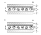
- FIG. 1 is a schematic cross-sectional view of a PDLC film in one embodiment of the present invention.
- a polymer dispersed liquid crystal film according to an embodiment of the present invention includes a first transparent conductive film, a polymer dispersed liquid crystal layer, and a second transparent conductive film, in this order.
- the polymer dispersed liquid crystal layer includes a polymer matrix and droplets (hereinafter, sometimes referred to as "liquid crystal droplets") that are dispersed in the polymer matrix and contain a liquid crystal component and a dichroic dye.
- the droplets have an average particle size of 1 ⁇ m or less and a clarity of 90 or more in a colored state.
- the appearance of the PDLC film changes depending on the applied voltage.
- the PDLC film is transparent when a voltage is applied and colored when no voltage is applied (normal mode).
- the PDLC film is colored when a voltage is applied and transparent when no voltage is applied (reverse mode).
- FIG. 1 is a schematic cross-sectional view illustrating the configuration of an example of a normal mode PDLC film according to an embodiment of the present invention, in which FIG. 1(a) shows a state in which no voltage is applied to the PDLC layer (colored state), and FIG. 1(b) shows a state in which a voltage is applied to the PDLC layer (transparent state).
- the PDLC film 100 includes, in this order, a first transparent conductive film 10, a PDLC layer 20 including a polymer matrix 22 and liquid crystal droplets 25 dispersed in the polymer matrix 22, and a second transparent conductive film 30.
- the liquid crystal droplets 25 are so-called guest-host liquid crystals that contain a liquid crystal component 23 and a dichroic dye 24. As shown in FIG.
- an alignment film is provided on the surface of the transparent conductive film, which aligns the liquid crystal component 23 and dichroic dye 24 in the liquid crystal droplets 25 when no voltage is applied, resulting in a transparent state, and when a voltage is applied, the alignment state of the liquid crystal component 23 and dichroic dye 24 changes, resulting in a colored state.
- the clarity of the PDLC film in the colored state is, for example, 90 or more, preferably 92 or more, more preferably 95 or more, and even more preferably 97 or more.
- the upper limit of clarity is 100. Clarity corresponds to the narrow-angle scattering degree, and is the transmittance in an angular range of ⁇ 2.5° with respect to the traveling direction of the parallel light of light incident on the PDLC film. High clarity means that the boundary of the image seen through the PDLC film is clear.
- Clarity is calculated by the following formula (1), where the amount of light L C is the amount of straight light traveling straight with respect to the optical axis of the parallel light of the light incident on the PDLC film, and the amount of narrow-angle scattered light whose angle with respect to the optical axis of the parallel light is within ⁇ 2.5°, among the light transmitted through the PDLC film, is the amount of light L R. 100 ⁇ (L C ⁇ L R )/(L C +L R ) ... Formula (1)
- the total light transmittance of the PDLC film in the colored state is, for example, 50% or less, and may be 40% or less, 30% or less, 20% or less, or 10% or less, and may be, for example, 0.5% or more, and may be 1% or more.
- the total light transmittance of the PDLC film in the transparent state is, for example, 15% or more, and may be 20% or more, 30% or more, or 50% or more, and may be, for example, 99% or less.
- the difference in the total light transmittance of the PDLC film in the transparent and colored states is, for example, 10% or more, and may be 20% or more, or 30% or more.
- the total light transmittance may be measured in accordance with JIS K 7361.
- the haze of the PDLC film in the colored state is, for example, 80% or less, and may be 60% or less, 50% or less, or 45% or less, for example, 5% or more.
- the haze of the PDLC film in the transparent state is, for example, 30% or less, and may be 20% or less, 10% or less, or 5% or less, for example, 0.1% or more.
- the difference in haze between the transparent and colored states of the PDLC film is, for example, 10% or more, and may be 20% or more, 30% or more, or 40% or more.
- the haze may be measured according to JIS K 7136.
- the voltage applied to the PDLC film when voltage is applied is a voltage that can operate the PDLC film (operating voltage), and can be, for example, 5 V to 300 V, and preferably 10 V to 200 V.
- "when voltage is applied” means a state in which an operating voltage is applied to the PDLC film, and can be, for example, a state in which a voltage of 150 V is applied.
- the first transparent conductive film 10 typically has a first transparent substrate 12 and a first transparent electrode layer 14 provided on one side (the PDLC layer 20 side) of the first transparent substrate 12.
- the first transparent conductive film 10 may have a hard coat layer on one or both sides of the first transparent substrate 12, and may also have a refractive index adjustment layer between the first transparent substrate 12 and the first transparent electrode layer 14, as necessary.
- the surface resistance of the first transparent conductive film is preferably 1 ⁇ / ⁇ to 1000 ⁇ / ⁇ , more preferably 5 ⁇ / ⁇ to 300 ⁇ / ⁇ , and even more preferably 10 ⁇ / ⁇ to 200 ⁇ / ⁇ .
- the haze value of the first transparent conductive film is preferably 20% or less, more preferably 10% or less, and even more preferably 0.1% to 10%.
- the total light transmittance of the first transparent conductive film is preferably 40% or more, more preferably 60% or more, and even more preferably 80% or more.
- the first transparent substrate may be formed using any suitable material.
- the first transparent substrate is a polymer film mainly composed of a thermoplastic resin.
- thermoplastic resins include polyester resins; cycloolefin resins such as polynorbornene; acrylic resins; polycarbonate resins; cellulose resins, etc.
- polyester resins, cycloolefin resins, and acrylic resins are preferred. These resins are excellent in transparency, mechanical strength, thermal stability, moisture shielding properties, etc.
- the above thermoplastic resins may be used alone or in combination of two or more kinds.
- optical films such as those used in polarizing plates, such as low retardation substrates, high retardation substrates, retardation plates, absorptive polarizing films, and polarized selective reflection films, can also be used as the first transparent substrate.
- the thickness of the first transparent substrate is preferably 200 ⁇ m or less, more preferably 3 ⁇ m to 100 ⁇ m, and even more preferably 5 ⁇ m to 70 ⁇ m. By making the thickness of the first transparent substrate 200 ⁇ m or less, the function of the PDLC layer can be fully exhibited.
- the total light transmittance of the first transparent substrate is preferably 40% or more, more preferably 60% or more, and even more preferably 80% or more.
- the first transparent electrode layer may be formed using a metal oxide such as indium tin oxide (ITO), zinc oxide (ZnO), or tin oxide (SnO 2 ).
- the metal oxide may be an amorphous metal oxide or a crystallized metal oxide.
- the first transparent electrode layer may also be formed by a metal nanowire such as silver nanowire (AgNW), a carbon nanotube (CNT), an organic conductive film, a metal layer, or a laminate thereof.
- a transparent electrode layer containing ITO is preferably formed.
- the transparent electrode layer containing ITO has excellent transparency.
- the first transparent electrode layer may be patterned into a desired shape depending on the purpose.
- the total light transmittance of the first transparent electrode layer is preferably 85% or more, more preferably 87% or more, and even more preferably 90% or more.
- a transparent electrode layer having a total light transmittance in this range a PDLC film having a high total light transmittance in the transparent state can be obtained.
- the thickness of the first transparent electrode layer is, for example, 10 nm or more, and preferably 15 nm or more.
- the thickness of the first transparent electrode layer is, for example, 50 nm or less, preferably 35 nm or less, and more preferably 30 nm or less.
- the first transparent electrode layer is provided on one side of the first transparent substrate, for example, by sputtering. After forming the metal oxide layer by sputtering, it can be crystallized by annealing. Annealing is performed, for example, by heat treatment at 120°C to 300°C for 10 to 120 minutes.
- the refractive index adjustment layer and hard coat layer may have configurations that are well known in the art, so detailed descriptions of their configurations will be omitted.
- the PDLC layer 20 includes a polymer matrix 22 and liquid crystal droplets 25 dispersed in the polymer matrix 22.
- the average particle size of the liquid crystal droplets is typically 1 ⁇ m or less, for example, 0.5 ⁇ m or less. Since a PDLC layer including liquid crystal droplets with a small particle size has low scattering properties, a PDLC film with high clarity can be obtained by setting the average particle size of the liquid crystal droplets to 1 ⁇ m or less. From the viewpoint of further reducing scattering properties, it is preferable that the average particle size of the liquid crystal droplets is equal to or less than the wavelength of visible light.
- the average particle size of the liquid crystal droplets is preferably less than 0.38 ⁇ m, more preferably less than 0.3 ⁇ m, even more preferably less than 0.2 ⁇ m, even more preferably 0.18 ⁇ m or less, even more preferably 0.15 ⁇ m or less, and even more preferably 0.12 ⁇ m or less.
- the lower limit of the average particle size of the liquid crystal droplets is not limited as long as the effects of the present invention are obtained, and may be, for example, 0.01 ⁇ m or more or 0.05 ⁇ m or more.
- the average particle size of the liquid crystal droplets is a volume average particle size, and can be determined, for example, by the method described in the Examples.
- the particle size of the liquid crystal droplets preferably has a relatively narrow particle size distribution.
- the coefficient of variation (CV value) of the particle size of the liquid crystal droplets may be, for example, less than 0.4, preferably 0.35 or less, and more preferably 0.3 or less.
- the coefficient of variation can be calculated from the following formula.
- CV value standard deviation of particle size distribution of liquid crystal droplets / average particle size
- the polymer matrix may be composed of any appropriate resin.
- the resin for forming the polymer matrix may be appropriately selected depending on the light transmittance, the refractive index of the liquid crystal component, the adhesion to the transparent conductive film, etc. It is preferable that the resin for forming the polymer matrix has a refractive index close to that of the liquid crystal component.
- resins for forming polymer matrices include urethane-based resins, polyvinyl alcohol-based resins, polyethylene-based resins, polypropylene-based resins, acrylic-based resins, etc. These are preferably water-soluble resins or water-dispersible resins. Only one type of resin for forming polymer matrices may be used, or two or more types may be used in combination.
- any suitable liquid crystal compound can be used alone or in combination of two or more kinds.
- the birefringence is preferably 0.2 or less, more preferably 0.15 or less, and may be, for example, 0.12 or less, or for example, 0.1 or less.
- the birefringence is, for example, 0.01 or more, and may be 0.05 or more, or 0.08 or more.
- liquid crystal component having the above birefringence By using a liquid crystal component having the above birefringence, it is possible to reduce the scattering property of the PDLC layer in a colored state (for example, when no voltage is applied), and as a result, it is possible to obtain a PDLC film with high clarity.
- the dielectric anisotropy of the liquid crystal component may be positive or negative.
- the liquid crystal component may be, for example, a nematic liquid crystal, a smectic liquid crystal, or a cholesteric liquid crystal. It is preferable to use a nematic liquid crystal, since it can achieve excellent transparency in the transparent state.
- Nematic liquid crystal compounds include biphenyl compounds, phenylbenzoate compounds, cyclohexylbenzene compounds, azoxybenzene compounds, azobenzene compounds, azomethine compounds, terphenyl compounds, biphenylbenzoate compounds, cyclohexylbiphenyl compounds, phenylpyridine compounds, cyclohexylpyrimidine compounds, cholesterol compounds, fluorine compounds, etc.
- dichroic dye Any appropriate dichroic dye that is compatible with the liquid crystal component can be used as the dichroic dye.
- the dichroic dye may have a positive or negative ⁇ .
- the dichroic dye itself may exhibit liquid crystallinity. Only one type of dichroic dye may be used, or two or more types may be used in combination.
- dichroic dyes include azo dyes, anthraquinone dyes, naphthoquinone dyes, perylene dyes, quinophthalone dyes, tetrazine dyes, and benzothiadiazole dyes.
- the dichroic dye contains anthraquinone dyes or azo dyes.
- azo dyes for example, the azo dyes, anthraquinone dyes, or mixtures thereof described in "Liquid Crystal Device Handbook," edited by the 142nd Committee of the Japan Society for the Promotion of Science, Nihon Kogyo Shimbunsha (1989), pages 192 to 196 and 724 to 730, can be used.
- various dichroic dyes are commercially available, and these can be used as appropriate.
- the PDLC layer may further contain any appropriate component, as necessary.
- Such optional components include surfactants, leveling agents, crosslinking agents, dispersion stabilizers, etc.
- the content of the liquid crystal component in the PDLC layer is, for example, 30% to 90% by weight, preferably 35% to 85% by weight, and more preferably 40% to 80% by weight.
- the content of the dichroic dye in the PDLC layer is, for example, 0.1 to 20 parts by weight, preferably 1 to 15 parts by weight, and more preferably 3 to 10 parts by weight, per 100 parts by weight of the liquid crystal component.
- the weight ratio (former:latter) of the polymer matrix content to the total content of the liquid crystal component and dichroic dye in the PDLC layer is, for example, 10:90 to 70:30, preferably 15:85 to 65:35, and more preferably 20:80 to 60:40.
- the total content of the polymer matrix, liquid crystal component, and dichroic dye in the PDLC layer is, for example, 80% by weight or more, preferably 90% by weight or more, and more preferably 95% by weight or more, and is, for example, 100% by weight or less, and preferably 99% by weight or less.
- the thickness of the PDLC layer is preferably 40 ⁇ m or less, more preferably 30 ⁇ m or less, for example 25 ⁇ m or less, or for example 20 ⁇ m or less, and is preferably 2 ⁇ m or more, more preferably 3 ⁇ m or more, for example 5 ⁇ m or more, or for example 10 ⁇ m or more.
- a PDLC film having high clarity and high colorability can be suitably obtained.
- the second transparent conductive film 30 typically has a second transparent substrate 32 and a second transparent electrode layer 34 provided on one side (the PDLC layer 20 side) of the second transparent substrate 32.
- the second transparent conductive film 30 may have a hard coat layer on one or both sides of the second transparent substrate 32, and may also have a refractive index adjustment layer between the second transparent substrate 32 and the second transparent electrode layer 34, as necessary.
- the surface resistance of the second transparent conductive film is preferably 1 ⁇ / ⁇ to 1000 ⁇ / ⁇ , more preferably 5 ⁇ / ⁇ to 300 ⁇ / ⁇ , and even more preferably 10 ⁇ / ⁇ to 200 ⁇ / ⁇ .
- the haze value of the second transparent conductive film is preferably 20% or less, more preferably 10% or less, and even more preferably 0.1% to 10%.
- the total light transmittance of the second transparent conductive film is preferably 40% or more, more preferably 60% or more, and even more preferably 80% or more.
- the same explanations as for the first transparent substrate and the first transparent electrode layer can be applied to the second transparent substrate and the second transparent electrode layer, respectively.
- the second transparent conductive film may have the same configuration as the first transparent conductive film, or may have a different configuration.
- the PDLC film described in Section A can be produced by any suitable production method.
- the method for producing the PDLC film described in Section A can be, for example, mixing a liquid crystal component, a dichroic dye, and a dispersion medium to prepare a liquid crystal emulsion containing particles containing the liquid crystal component and the dichroic dye (Step A); mixing the liquid crystal emulsion with a polymer matrix forming resin to prepare a coating liquid containing the particles (step B); applying the coating liquid to a first transparent conductive film to obtain a coating layer (step C); drying the coating layer to obtain a PDLC layer comprising a polymer matrix and droplets containing the liquid crystal component and the dichroic dye dispersed in the polymer matrix (step D); and laminating a second transparent conductive film over the PDLC layer (Step E); Includes.
- Step A a liquid crystal component, a dichroic dye, and a dispersion medium are mixed to prepare a liquid crystal emulsion containing particles (hereinafter sometimes referred to as "liquid crystal particles") that contain the liquid crystal component and the dichroic dye.
- liquid crystal particles a liquid crystal emulsion containing particles
- water or a mixed solvent of water and a water-miscible organic solvent can be preferably used.
- water-miscible organic solvents include C1-3 alcohol, acetone, DMSO, etc.
- the liquid crystal component and dichroic dye are as described in Section A.
- the liquid crystal emulsion contains, for example, 30% to 70% by weight of liquid crystal components, and preferably 40% to 60% by weight.
- the content of the dichroic dye in the liquid crystal emulsion is, for example, 0.1 to 20 parts by weight, preferably 1 to 15 parts by weight, and more preferably 3 to 10 parts by weight, per 100 parts by weight of the liquid crystal component.
- the average particle size of the liquid crystal particles is typically 1 ⁇ m or less, for example 0.5 ⁇ m or less, preferably less than 0.38 ⁇ m, more preferably less than 0.3 ⁇ m, even more preferably less than 0.2 ⁇ m, even more preferably 0.18 ⁇ m or less, even more preferably 0.15 ⁇ m or less, even more preferably 0.12 ⁇ m or less, and may be, for example, 0.01 ⁇ m or more or 0.05 ⁇ m or more.
- the particle size of the liquid crystal droplets in the PDLC layer may depend on the particle size of the liquid crystal particles in the liquid crystal emulsion.
- the average particle size of the liquid crystal particles in the liquid crystal emulsion is within the above range, the average particle size of the liquid crystal droplets in the PDLC layer can be set to the desired range.
- the average particle size of the liquid crystal particles means the volume average median size, and can be measured using a dynamic light scattering particle size distribution measuring device.
- the particle diameter of the liquid crystal particles preferably has a relatively narrow particle size distribution.
- the coefficient of variation (CV value) of the liquid crystal particles may be, for example, less than 0.4, preferably 0.35 or less, and more preferably 0.3 or less.
- the liquid crystal emulsion can be prepared by, for example, a mechanical emulsification method, a microchannel method, a membrane emulsification method, or the like.
- the liquid crystal emulsion is prepared by a mechanical emulsification method or a membrane emulsification method.
- a liquid crystal emulsion having a small particle size can be efficiently obtained by a mechanical emulsification method.
- the mechanical emulsification method can be performed using a known dispersion/mixing device such as a homomixer or a homogenizer, and preferably a homogenizer such as a high-pressure homogenizer or an ultrasonic homogenizer.
- the membrane emulsification method can suitably obtain an emulsion with a uniform particle size distribution.
- the membrane emulsification method refer to the disclosures of JP-A-4-355719, JP-A-2015-40994, etc. (these are incorporated herein by reference).
- liquid crystal component, dichroic dye, and dispersion medium are mixed is not particularly limited.
- the liquid crystal component and the dichroic dye may be mixed, and the resulting mixture may be mixed with the dispersion medium, or the three may be added and mixed simultaneously.
- step B the liquid crystal emulsion obtained in step A is mixed with a polymer matrix forming resin to prepare a coating liquid containing the liquid crystal particles.
- the coating liquid may contain any other components as necessary. Examples of the optional components include a surfactant, a leveling agent, a crosslinking agent, a dispersion stabilizer, etc. These optional components may be added to the liquid crystal emulsion in step A depending on the purpose.
- the polymer matrix resin is as described in Section A.
- the polymer matrix resin is mixed with the liquid crystal emulsion, for example, as a resin dispersion in which polymer matrix resin particles are dispersed in a dispersion medium, or as a resin solution in which the polymer matrix resin is dissolved in a solvent.
- the dispersion medium of the resin dispersion or the solvent of the resin solution may be the same as the dispersion medium used in preparing the liquid crystal emulsion.
- the average particle size of the resin particles for forming the polymer matrix is preferably 10 nm to 500 nm, more preferably 30 nm to 300 nm, and even more preferably 50 nm to 200 nm. Two or more types of resin particles with different resin types and/or average particle sizes may be used.
- the average particle size of the resin particles for forming the polymer matrix means the volume-average median size, and can be measured using a dynamic light scattering particle size distribution measuring device.
- the particle size of the liquid crystal particles in the coating liquid is substantially the same as the particle size in the liquid crystal emulsion. Therefore, the average particle size (volume average particle size) of the liquid crystal particles in the coating liquid is typically 1 ⁇ m or less, for example 0.5 ⁇ m or less, preferably less than 0.38 ⁇ m, more preferably less than 0.3 ⁇ m, even more preferably less than 0.2 ⁇ m, even more preferably 0.18 ⁇ m or less, even more preferably 0.15 ⁇ m or less, even more preferably 0.12 ⁇ m or less, and may be, for example, 0.01 ⁇ m or more or 0.05 ⁇ m or more.
- the liquid crystal component content in the solid content of the coating liquid is, for example, 30% to 90% by weight, preferably 35% to 85% by weight, and more preferably 40% to 80% by weight.
- the weight ratio (former:latter) of the content of the polymer matrix-forming resin to the total content of the liquid crystal component and dichroic dye in the coating liquid is, for example, 10:90 to 70:30, preferably 15:85 to 65:35, and more preferably 20:80 to 60:40.
- the total content of the polymer matrix-forming resin, liquid crystal component, and dichroic dye in the solid content of the coating liquid is, for example, 80% by weight or more, preferably 90% by weight or more, and more preferably 95% by weight or more, and is, for example, 100% by weight or less, and preferably 99% by weight or less.
- surfactants examples include anionic surfactants, cationic surfactants, amphoteric surfactants, and nonionic surfactants.
- the surfactant content is preferably 1 to 15 parts by weight, and more preferably 2 to 10 parts by weight, per 100 parts by weight of the solid content of the coating liquid.
- leveling agents examples include acrylic leveling agents, fluorine-based leveling agents, and silicone-based leveling agents.
- the content of the leveling agent is preferably 0.1 to 10 parts by weight, and more preferably 0.5 to 5 parts by weight, per 100 parts by weight of the solid content of the coating liquid.
- crosslinking agents examples include aziridine-based crosslinking agents and isocyanate-based crosslinking agents.
- the content of the crosslinking agent is preferably 0.5 to 20 parts by weight, and more preferably 1 to 10 parts by weight, per 100 parts by weight of the solid content of the coating liquid.
- the solids concentration of the coating liquid can be, for example, 20% to 60% by weight, preferably 30% to 50% by weight.
- step C the coating liquid prepared in step B is applied to the first transparent conductive film to obtain a coating layer.
- the coating liquid is typically applied to the transparent electrode layer side surface of the first transparent conductive film.
- the first transparent conductive film is as described in Section A.
- the viscosity of the coating liquid during application is preferably 20 mPa ⁇ s to 400 mPa ⁇ s, more preferably 30 mPa ⁇ s to 300 mPa ⁇ s, and even more preferably 40 mPa ⁇ s to 200 mPa ⁇ s. If the viscosity is less than 20 mPa ⁇ s, convection of the dispersion medium becomes significant when the dispersion medium is dried, and the thickness of the PDLC layer may become unstable. If the viscosity exceeds 400 mPa ⁇ s, the bead of the coating liquid may become unstable.
- the viscosity of the coating liquid can be measured, for example, using an Anton Paar rheometer MCR302.
- the viscosity used here is the shear viscosity value at 20°C and a shear rate of 1000 (1/s).
- any appropriate method can be used as the coating method. Examples include roll coating, spin coating, bar coating, dip coating, die coating, curtain coating, spray coating, and knife coating (comma coating, etc.). Of these, roll coating is preferred. For example, the description of JP2019-5698A can be referred to for coating by the roll coating method using a slot die.
- the thickness of the coating layer is preferably 1 ⁇ m to 100 ⁇ m, more preferably 2 ⁇ m to 90 ⁇ m, and even more preferably 5 ⁇ m to 75 ⁇ m.
- step D the coating layer is dried to obtain a PDLC layer containing a polymer matrix and droplets containing a liquid crystal component and a dichroic dye dispersed in the polymer matrix.
- the dispersion medium is removed from the coating layer by drying, leaving behind the resin for forming the polymer matrix and particles containing the liquid crystal component, resulting in the formation of a PDLC layer having a structure in which liquid crystal droplets are dispersed in a polymer matrix.
- the coating layer can be dried by any appropriate method. Specific examples of drying methods include natural drying, heat drying, and hot air drying. If the coating liquid contains a crosslinking agent, a crosslinked structure of the polymer matrix can be formed during drying.
- the drying temperature is preferably 20°C to 150°C, more preferably 25°C to 80°C.
- the drying time is preferably 1 minute to 100 minutes, more preferably 2 minutes to 10 minutes.
- step E a second transparent conductive film is laminated on the PDLC layer, thereby obtaining a PDLC film having the first transparent conductive film, the PDLC layer, and the second transparent conductive film in this order.
- the second transparent conductive film is as described in section A.
- the second transparent conductive film is typically laminated onto the PDLC layer so that the second transparent electrode layer faces the PDLC layer.
- the lamination is preferably performed using a laminator while applying a lamination pressure of 0.006 MPa/m to 7 MPa/m, more preferably 0.06 MPa/m to 0.7 MPa/m.
- Thickness Measurement was performed using a digital micrometer (manufactured by Anritsu Corporation, product name "KC-351C”).
- Volume average particle size of liquid crystal particles in liquid crystal emulsion A measurement sample was prepared by adding a few drops of liquid crystal emulsion to 100 mL of water. Using a dynamic light scattering particle size distribution measurement device (manufactured by Microtrac, device name "Nanotrac 150"), the measurement sample was set in the measurement holder of the device, and the device monitor was used to confirm that the concentration was measurable, after which measurement was performed.
- (3) Average particle size of resin particles A few drops of the resin dispersion were added to 100 mL of water to prepare a measurement sample.
- Clarity Measurement was performed using a haze meter (manufactured by BYK-GARDNER, product name "haze-gard i") according to the method specified by the manufacturer.
- (7) Average particle size of liquid crystal droplets in PDLC layer The PDLC film was sliced horizontally under a cooling environment, and the horizontal cross section of the exposed PDLC layer was smoothed by a microtome. The horizontal cross section of the PDLC layer was then observed with a scanning electron microscope (SEM) to obtain a cross-sectional SEM image.
- SEM scanning electron microscope
- the Heywood diameter was calculated from the cross-sectional area of all liquid crystal droplets in a region of 30 ⁇ m ⁇ 20 ⁇ m in the cross-sectional SEM image, and the volume average particle size (median diameter) was calculated by taking statistics weighted by the volume estimated for each equivalent diameter.
- Birefringence of Liquid Crystal Component The value disclosed by the manufacturer of the liquid crystal component was used.
- Example 1 (First and second transparent conductive films) An ITO layer was formed by sputtering on one surface of a PET substrate (thickness: 50 ⁇ m) to obtain a transparent conductive film having a structure of [transparent substrate/transparent electrode layer].
- a PDLC film (Preparation of PDLC Film)
- the emulsion coating liquid was applied to the ITO layer surface of the first transparent conductive film and dried at 40° C. to form a PDLC layer with a thickness of 16 ⁇ m.
- a second transparent conductive film was laminated on the PDLC layer with the ITO layer facing the PDLC layer while applying a lamination pressure of 0.4 MPa/m using a laminator. This resulted in a PDLC film.
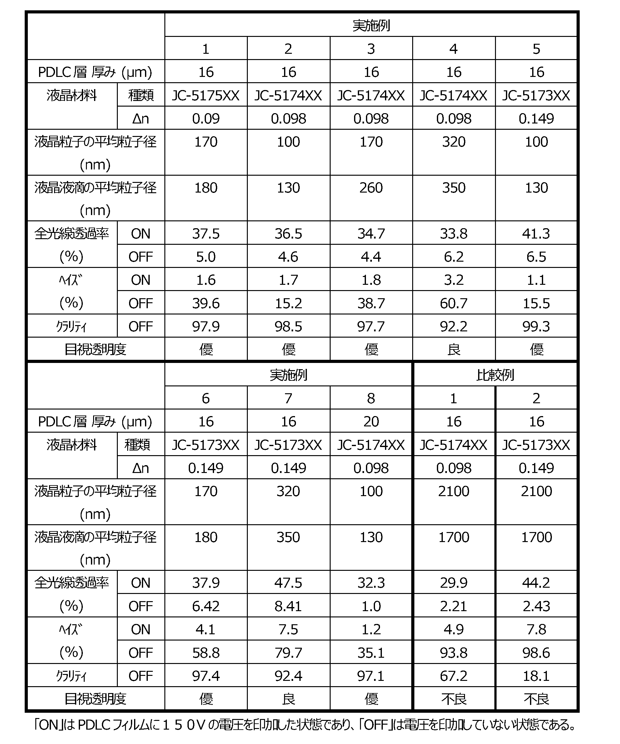
- Examples 2 to 8 PDLC films were obtained in the same manner as in Example 1, except that different types of liquid crystal components were used, liquid crystal emulsions with different average particle sizes of the liquid crystal particles were prepared, and/or the thickness of the PDLC layer was changed, as shown in Table 1.
- the properties of the liquid crystal components used are as follows.
- the crude dispersion was passed through a separation membrane with a uniform particle size distribution (SPG Techno, "SPG Pumping Connector", pore size 5 ⁇ m) at room temperature from the outside to the inside of the membrane at a flow rate of 80 mL/min/cm 2. This operation was performed 10 times.
- the volume average particle size of the liquid crystal particles in the obtained liquid crystal emulsion was 2.1 ⁇ m.
- a PDLC film (Preparation of PDLC Film)
- the emulsion coating liquid was applied to the ITO layer surface of the first transparent conductive film and dried at 40° C. to form a PDLC layer with a thickness of 16 ⁇ m.
- a second transparent conductive film was laminated on the PDLC layer with the ITO layer facing the PDLC layer while applying a lamination pressure of 0.4 MPa/m using a laminator. This resulted in a PDLC film.
- Comparative Example 2 As shown in Table 1, a PDLC film was obtained in the same manner as in Comparative Example 1, except that a different type of liquid crystal component was used.
- ⁇ Visual transparency evaluation> The visual transparency was evaluated based on the visibility of the characters when plain paper on which characters were printed in black ink was visually observed through the PDLC film (colored state with no voltage applied) obtained in the examples and comparative examples.
- the distance between the plain paper and the PDLC film was about 200 mm, and the distance from the observer's eye to the plain paper was 200 mm.
- the evaluation results are shown in Table 1 together with the clarity, total light transmittance, and haze of each PDLC film. Evaluation Criteria Excellent: Very high transparency, allowing characters to be clearly read. Good: Transparency is moderately high and characters are visible. Poor: The transparency is low and the characters cannot be seen.
- the PDLC film of the embodiment exhibited low scattering in the colored state and high clarity.
- the PDLC film of the present invention is suitable for use in a variety of applications, including advertising, signs, smart windows, etc.
- Reference Signs List 100 PDLC film 10 First transparent conductive film 20 PDLC layer 22 Polymer matrix 23 Liquid crystal component 24 Dichroic dye 25 Liquid crystal droplet 30 Second transparent conductive film
Landscapes
- Physics & Mathematics (AREA)
- Nonlinear Science (AREA)
- Chemical & Material Sciences (AREA)
- Crystallography & Structural Chemistry (AREA)
- General Physics & Mathematics (AREA)
- Optics & Photonics (AREA)
- Dispersion Chemistry (AREA)
- Mathematical Physics (AREA)
- Liquid Crystal (AREA)
Abstract
Description
[2]上記[1]に記載の高分子分散型液晶フィルムにおいて、上記液滴の平均粒子径が、0.01μm以上0.38μm未満であってよい。
[3]上記[1]または[2]に記載の高分子分散型液晶フィルムにおいて、上記液晶成分の複屈折が、0.25以下であってよい。
[4]上記[1]から[3]のいずれかに記載の高分子分散型液晶フィルムにおいて、上記高分子分散型液晶層における上記高分子マトリクスの含有量と上記液晶成分および上記二色性色素の合計含有量との重量比(前者:後者)が、10:90~70:30であってよい。
[5]上記[1]から[4]のいずれかに記載の高分子分散型液晶フィルムにおいて、上記高分子分散型液晶層の厚みが、30μm以下であってよい。
[6]上記[1]から[5]のいずれかに記載の高分子分散型液晶フィルムにおいて、着色状態における全光線透過率が、50%以下であってよい。
[7]上記[1]から[6]のいずれかに記載の高分子分散型液晶フィルムにおいて、着色状態におけるヘイズが、80%以下であってよい。
本発明の実施形態による高分子分散型液晶フィルムは、第1の透明導電性フィルムと、高分子分散型液晶層と、第2の透明導電性フィルムと、をこの順に含み、上記高分子分散型液晶層が、高分子マトリクスと、上記高分子マトリクス中に分散しており、液晶成分と二色性色素とを含む液滴(以下、「液晶液滴」と称する場合がある)と、を含み、上記液滴の平均粒子径が、1μm以下であり、着色状態におけるクラリティが、90以上である。
100×(LC-LR)/(LC+LR) … 式(1)
第1の透明導電性フィルム10は、代表的には、第1の透明基材12とその一方の側(PDLC層20側)に設けられた第1の透明電極層14とを有する。第1の透明導電性フィルム10は、必要に応じて、第1の透明基材12の片側または両側にハードコート層を有していてもよく、また、第1の透明基材12と第1の透明電極層14との間に屈折率調整層を有していてもよい。
PDLC層20は、高分子マトリクス22と高分子マトリクス22中に分散した液晶液滴25とを含む。液晶液滴の平均粒子径は、代表的には1μm以下であり、例えば0.5μm以下である。粒子径が小さい液晶液滴を含むPDLC層は散乱性が低くなることから、液晶液滴の平均粒子径を1μm以下とすることにより、クラリティが高いPDLCフィルムが得られ得る。散乱性をより低くする観点から、液晶液滴の平均粒子径は、可視光の波長以下であることが好ましい。具体的には、液晶液滴の平均粒子径は、好ましくは0.38μm未満、より好ましくは0.3μm未満、さらに好ましくは0.2μm未満、さらにより好ましくは0.18μm以下、さらにより好ましくは0.15μm以下、さらにより好ましくは0.12μm以下である。液晶液滴の平均粒子径の下限は、本発明の効果が得られる限り制限されず、例えば0.01μm以上または0.05μm以上であり得る。上記液晶液滴の平均粒子径は、体積平均粒子径であり、例えば、実施例に記載の方法で求めることができる。
CV値=液晶液滴の粒子径分布の標準偏差/平均粒子径
第2の透明導電性フィルム30は、代表的には、第2の透明基材32とその一方の側(PDLC層20側)に設けられた第2の透明電極層34とを有する。第2の透明導電性フィルム30は、必要に応じて、第2の透明基材32の片側または両側にハードコート層を有していてもよく、また、第2の透明基材32と第2の透明電極層34との間に屈折率調整層を有していてもよい。
A項に記載のPDLCフィルムは、任意の適切な製造方法で製造することができる。A項に記載のPDLCフィルムの製造方法は、例えば、
液晶成分と二色性色素と分散媒とを混合して、上記液晶成分と上記二色性色素とを含有する粒子を含む液晶エマルションを調製すること(工程A)、
上記液晶エマルションと高分子マトリクス形成用樹脂とを混合して、上記粒子を含む塗工液を調製すること(工程B)、
第1の透明導電性フィルムに、上記塗工液を塗工して、塗布層を得ること(工程C)、
該塗布層を乾燥させて、高分子マトリクスと上記高分子マトリクス中に分散した上記液晶成分および上記二色性色素を含有する液滴とを含むPDLC層を得ること(工程D)、および、
上記PDLC層の上に第2の透明導電性フィルムを積層すること(工程E)、
を含む。
工程Aにおいては、液晶成分と二色性色素と分散媒とを混合して、上記液晶成分と二色性色素とを含有する粒子(以下、「液晶粒子」と称する場合がある)を含む液晶エマルションを調製する。
工程Bにおいては、工程Aで得られた液晶エマルションと高分子マトリクス形成用樹脂とを混合して、上記液晶粒子を含む塗工液を調製する。塗工液は、必要に応じて、任意の他の成分を含み得る。任意成分としては、界面活性剤、レベリング剤、架橋剤、分散安定剤等が挙げられる。これらの任意成分は、目的に応じて、工程Aにおいて液晶エマルションに添加されていてもよい。
工程Cにおいては、第1の透明導電性フィルムに、B項で調製した塗工液を塗布して、塗布層を得る。
工程Dにおいては、塗布層を乾燥させて、高分子マトリクスと該高分子マトリクス中に分散した液晶成分および二色性色素を含有する液滴とを含むPDLC層を得る。乾燥により塗布層から分散媒が除去されて高分子マトリクス形成用樹脂と液晶成分を含む粒子が残存する結果、高分子マトリクス中に液晶液滴が分散した構造を有するPDLC層が形成される。
工程Eにおいては、PDLC層の上に第2の透明導電性フィルムを積層する。これにより、第1の透明導電性フィルムと、PDLC層と、第2の透明導電性フィルムとをこの順に有するPDLCフィルムが得られる。
デジタルマイクロメーター(アンリツ社製、製品名「KC-351C」)を用いて測定した。
(2)液晶エマルション中の液晶粒子の体積平均粒子径
100mLの水に液晶エマルションを数滴加えて測定試料を調製した。動的光散乱式粒子径分布測定装置(Microtrac社製、装置名「Nanotrac150」)を用いて、装置の測定ホルダに測定試料をセットし、測定可能な濃度であることを装置のモニタにて確認後に測定を行った。
(3)樹脂粒子の平均粒子径
100mLの水に樹脂分散体を数滴加えて測定試料を調製した。動的光散乱式粒子径分布測定装置(Microtrac社製、装置名「Nanotrac150」)を用いて、装置の測定ホルダに測定試料をセットし、測定可能な濃度であることを装置のモニタにて確認後に測定を行った。
(4)ヘイズ
ヘイズメーター(日本電色社製、製品名「NDH4000」)を用いて、JIS K 7136に基づいて測定した。
(5)全光線透過率
ヘイズメーター(日本電色社製、製品名「NDH4000」)を用いて、JIS K 7361に基づいて測定した。
(6)クラリティ
ヘイズメーター(BYK-GARDNER社製、製品名「haze-gard i」)を用いて、メーカー指定の方法に基づいて測定した。
(7)PDLC層中の液晶液滴の平均粒子径
冷却環境下でPDLCフィルムを水平方向にスライスし、露出したPDLC層の水平断面をミクロトームにより平滑化した。次いで、PDLC層の水平断面を走査型電子顕微鏡(SEM)にて観察し、断面SEM画像を得た。断面SEM画像中、30μm×20μmの領域における全ての液晶液滴の断面積から面積円相当径(Heywood diameter)を算出し、相当径ごとに推定される体積で重み付けした統計を取ることで体積平均粒子径(メジアン径)を算出した。
(8)液晶成分の複屈折
液晶成分の製造業者が開示する値を用いた。
(第1および第2の透明導電性フィルム)
PET基材(厚み:50μm)の一方の面に、スパッタ法によりITO層を形成して、[透明基材/透明電極層]の構成を有する透明導電性フィルムを得た。
2種以上の液晶化合物を含む液晶成分(JNC社製、製品名「JC-5175XX」、複屈折Δn=0.09(ne=1.569,no=1.479、誘電率異方性Δε=7.9、粘度=32.2mPa・s)27.9部、二色性色素(林原社製、製品名「G-470」)0.26部、二色性色素(林原社製、製品名「NKX-3739」)0.53部、二色性色素(林原社製、製品名「NKX-3708」)1.31部、純水67部、および界面活性剤(第一工業製薬社製、「ノイゲンET159」)3部を混合し、高圧ホモジナイザーで処理することによって液晶エマルションを調製した。得られた液晶エマルション中の液晶粒子の平均粒子径は、170nmであった。
上記液晶エマルション47.6部、ポリエーテル系ポリウレタン樹脂水性分散体(DSM社製、商品名「NeoRezR967」、ポリマー平均粒子径:80nm、CV値=0.27、固形分:40wt%)32部、レベリング剤(DIC社製、製品名「F-444」)0.1部、架橋剤(トリス〔3-(2-メチルアジリジン-1-イル)プロピオン酸〕=プロピリジントリメチル)1部、および純水19.3部を混合することにより、エマルション塗工液(固形分濃度:30wt%)を得た。
上記エマルション塗工液を、第1の透明導電性フィルムのITO層面に塗布し、40℃で乾燥させて、厚み16μmのPDLC層を形成した。その後、ラミネーターを用いて0.4MPa/mのラミネート圧を適用しながら、上記PDLC層の上に第2の透明導電性フィルムを、ITO層がPDLC層に対向するように積層した。これにより、PDLCフィルムを得た。
表1に示すように、異なる種類の液晶成分を用いたこと、液晶粒子の平均粒子径が異なる液晶エマルションを調製したこと、および/またはPDLC層の厚みを変更したこと以外は実施例1と同様にして、PDLCフィルムを得た。用いた液晶成分の特性は以下のとおりである。
・液晶成分(JNC社製、製品名「JC-5174XX」、複屈折Δn=0.098(ne=1.577,no=1.479)、誘電率異方性Δε=11.8、粘度=46.8mPa・s)
・液晶成分(JNC社製、製品名「JC-5173XX」、複屈折Δn=0.149(ne=1.651,no=1.502)、誘電率異方性Δε=10.0、粘度=48.5mPa・s)
(第1および第2の透明導電性フィルム)
PET基材(厚み:50μm)の一方の面に、スパッタ法によりITO層を形成して、[透明基材/透明電極層]の構成を有する透明導電性フィルムを得た。
液晶成分(JNC社製、製品名「JC-5174XX」)27.9部、二色性色素(林原社製、製品名「G-470」)0.26部、二色性色素(林原社製、製品名「NKX-3739」)0.53部、二色性色素(林原社製、製品名「NKX-3708」)1.31部、純水67部、および界面活性剤(第一工業製薬社製、「ノイゲンET159」)3部を混合し、ホモジナイザーにて100rpmで10分攪拌して粗分散した。粗分散液を、粒度分布の揃った分離膜(エス・ピー・ジーテクノ社製、「SPGポンピングコネクター」、細孔径5μm)に、室温にて膜の外から内に通過するように流速80mL/分/cm2の速度で透過させた。この操作を10回実施した。得られた液晶エマルション中の液晶粒子の体積平均粒子径は2.1μmであった。
上記液晶エマルション47.6部、ポリエーテル系ポリウレタン樹脂水性分散体(DSM社製、商品名「NeoRezR967」、ポリマー平均粒子径:80nm、CV値=0.27、固形分:40wt%)32部、レベリング剤(DIC社製、製品名「F-444」)0.1部、架橋剤(トリス〔3-(2-メチルアジリジン-1-イル)プロピオン酸〕=プロピリジントリメチル)1部、および純水19.3部を混合することにより、エマルション塗工液(固形分濃度:30wt%)を得た。
上記エマルション塗工液を、第1の透明導電性フィルムのITO層面に塗布し、40℃で乾燥させて、厚み16μmのPDLC層を形成した。その後、ラミネーターを用いて0.4MPa/mのラミネート圧を適用しながら、上記PDLC層の上に第2の透明導電性フィルムを、ITO層がPDLC層に対向するように積層した。これにより、PDLCフィルムを得た。
表1に示すように、異なる種類の液晶成分を用いたこと以外は比較例1と同様にして、PDLCフィルムを得た。
黒インクで文字を印刷した普通紙を実施例および比較例で得たPDLCフィルム(電圧無印加の着色状態)を介して目視で観察した際の文字の視認性に基づいて、以下の基準で目視透明度を評価した。なお、普通紙とPDLCフィルムとの距離は約200mmであり、観察者の眼から普通紙までの距離は200mmであった。各PDLCフィルムのクラリティ、全光線透過率、およびヘイズと併せて評価結果を表1に示す。
≪評価基準≫
優:透明度が非常に高く、文字を明瞭に視認できる。
良:透明度がやや高く、文字を視認できる。
不良:透明度が低く、文字を視認できない。
10 第1の透明導電性フィルム
20 PDLC層
22 高分子マトリクス
23 液晶成分
24 二色性色素
25 液晶液滴
30 第2の透明導電性フィルム
Claims (7)
- 第1の透明導電性フィルムと、高分子分散型液晶層と、第2の透明導電性フィルムと、をこの順に含む、高分子分散型液晶フィルムであって、
前記高分子分散型液晶層が、高分子マトリクスと、前記高分子マトリクス中に分散しており、液晶成分と二色性色素とを含む液滴と、を含み、
前記液滴の平均粒子径が、1μm以下であり、
着色状態におけるクラリティが、90以上である、高分子分散型液晶フィルム。 - 前記液滴の平均粒子径が、0.01μm以上0.38μm未満である、請求項1に記載の高分子分散型液晶フィルム。
- 前記液晶成分の複屈折が、0.25以下である、請求項1に記載の高分子分散型液晶フィルム。
- 前記高分子分散型液晶層における前記高分子マトリクスの含有量と前記液晶成分および前記二色性色素の合計含有量との重量比(前者:後者)が、10:90~70:30である、請求項1に記載の高分子分散型液晶フィルム。
- 前記高分子分散型液晶層の厚みが、30μm以下である、請求項1に記載の高分子分散型液晶フィルム。
- 着色状態における全光線透過率が、50%以下である、請求項1に記載の高分子分散型液晶フィルム。
- 着色状態におけるヘイズが、80%以下である、請求項1に記載の高分子分散型液晶フィルム。
Priority Applications (3)
| Application Number | Priority Date | Filing Date | Title |
|---|---|---|---|
| US19/168,464 US20260110932A1 (en) | 2023-03-24 | 2024-03-07 | Polymer dispersion-type liquid crystal film |
| KR1020257030101A KR20250162540A (ko) | 2023-03-24 | 2024-03-07 | 고분자 분산형 액정 필름 |
| CN202480021253.9A CN120981761A (zh) | 2023-03-24 | 2024-03-07 | 高分子分散型液晶膜 |
Applications Claiming Priority (2)
| Application Number | Priority Date | Filing Date | Title |
|---|---|---|---|
| JP2023-048075 | 2023-03-24 | ||
| JP2023048075A JP7748980B2 (ja) | 2023-03-24 | 2023-03-24 | 高分子分散型液晶フィルム |
Publications (1)
| Publication Number | Publication Date |
|---|---|
| WO2024203117A1 true WO2024203117A1 (ja) | 2024-10-03 |
Family
ID=92905623
Family Applications (1)
| Application Number | Title | Priority Date | Filing Date |
|---|---|---|---|
| PCT/JP2024/008798 Ceased WO2024203117A1 (ja) | 2023-03-24 | 2024-03-07 | 高分子分散型液晶フィルム |
Country Status (6)
| Country | Link |
|---|---|
| US (1) | US20260110932A1 (ja) |
| JP (1) | JP7748980B2 (ja) |
| KR (1) | KR20250162540A (ja) |
| CN (1) | CN120981761A (ja) |
| TW (1) | TWI914749B (ja) |
| WO (1) | WO2024203117A1 (ja) |
Citations (4)
| Publication number | Priority date | Publication date | Assignee | Title |
|---|---|---|---|---|
| WO2019132009A1 (ja) * | 2017-12-28 | 2019-07-04 | 凸版印刷株式会社 | 調光シート、および、調光窓 |
| WO2019221167A1 (ja) * | 2018-05-15 | 2019-11-21 | 凸版印刷株式会社 | 調光装置、調光装置の管理方法、および、調光装置の製造方法 |
| JP2021196453A (ja) * | 2020-06-11 | 2021-12-27 | 凸版印刷株式会社 | 調光シート |
| US20220153097A1 (en) * | 2020-11-16 | 2022-05-19 | Imagelab Co., Ltd. | Light transmittance control panel for smart windows and smart window for vehicle with the same |
Family Cites Families (9)
| Publication number | Priority date | Publication date | Assignee | Title |
|---|---|---|---|---|
| JPH07234397A (ja) * | 1994-02-23 | 1995-09-05 | Hitachi Cable Ltd | ポリマ分散型液晶素子 |
| JP2002189123A (ja) | 2000-12-19 | 2002-07-05 | Hitachi Chem Co Ltd | 調光材料、調光フィルム及び調光フィルムの製造方法 |
| CN103885233B (zh) * | 2012-12-21 | 2017-05-24 | 北京众智同辉科技股份有限公司 | 一种彩色聚合物分散型液晶薄膜的制备方法 |
| KR101979778B1 (ko) * | 2015-02-16 | 2019-05-17 | 주식회사 엘지화학 | 액정 소자 |
| WO2022030296A1 (ja) * | 2020-08-07 | 2022-02-10 | 日東電工株式会社 | 視野角制御フィルム、バックライトユニットおよび液晶表示装置 |
| JP2022129507A (ja) * | 2021-02-25 | 2022-09-06 | 日東電工株式会社 | 加飾フィルム |
| WO2022186062A1 (ja) | 2021-03-01 | 2022-09-09 | 三菱ケミカル株式会社 | 液晶素子及びエマルジョン組成物 |
| JP7806599B2 (ja) | 2022-04-11 | 2026-01-27 | Toppanホールディングス株式会社 | 調光装置 |
| JP7260030B1 (ja) | 2022-04-11 | 2023-04-18 | 凸版印刷株式会社 | 調光装置 |
-
2023
- 2023-03-24 JP JP2023048075A patent/JP7748980B2/ja active Active
-
2024
- 2024-03-07 WO PCT/JP2024/008798 patent/WO2024203117A1/ja not_active Ceased
- 2024-03-07 KR KR1020257030101A patent/KR20250162540A/ko active Pending
- 2024-03-07 US US19/168,464 patent/US20260110932A1/en active Pending
- 2024-03-07 CN CN202480021253.9A patent/CN120981761A/zh active Pending
- 2024-03-22 TW TW113110750A patent/TWI914749B/zh active
Patent Citations (4)
| Publication number | Priority date | Publication date | Assignee | Title |
|---|---|---|---|---|
| WO2019132009A1 (ja) * | 2017-12-28 | 2019-07-04 | 凸版印刷株式会社 | 調光シート、および、調光窓 |
| WO2019221167A1 (ja) * | 2018-05-15 | 2019-11-21 | 凸版印刷株式会社 | 調光装置、調光装置の管理方法、および、調光装置の製造方法 |
| JP2021196453A (ja) * | 2020-06-11 | 2021-12-27 | 凸版印刷株式会社 | 調光シート |
| US20220153097A1 (en) * | 2020-11-16 | 2022-05-19 | Imagelab Co., Ltd. | Light transmittance control panel for smart windows and smart window for vehicle with the same |
Also Published As
| Publication number | Publication date |
|---|---|
| TW202442446A (zh) | 2024-11-01 |
| JP7748980B2 (ja) | 2025-10-03 |
| KR20250162540A (ko) | 2025-11-18 |
| US20260110932A1 (en) | 2026-04-23 |
| TWI914749B (zh) | 2026-02-11 |
| JP2024136816A (ja) | 2024-10-04 |
| CN120981761A (zh) | 2025-11-18 |
Similar Documents
| Publication | Publication Date | Title |
|---|---|---|
| US7387858B2 (en) | Reflective display based on liquid crystal materials | |
| WO2008005202A2 (en) | Single substrate guest-host polymer liquid crystal displays | |
| TWI827763B (zh) | 可切換窗元件 | |
| CN117897653A (zh) | 高分子分散型液晶膜及高分子分散型液晶膜的制造方法 | |
| CN116888526A (zh) | 装饰膜 | |
| US7382424B2 (en) | Reflective chiral-nematic liquid crystal display with broadband reflection | |
| CN120077324A (zh) | 液晶元件和乳液组合物 | |
| US20050264725A1 (en) | Reflective liquid crystal display with infrared reflection | |
| TW202348425A (zh) | 高分子分散型液晶膜、光學膜組、及高分子分散型液晶膜之製造方法 | |
| CN115362409A (zh) | 高分子分散型液晶膜、乳液、以及高分子分散型液晶膜的制造方法 | |
| JP7748980B2 (ja) | 高分子分散型液晶フィルム | |
| CN117120920A (zh) | 高分子分散型液晶薄膜及其制造方法 | |
| CN116981987A (zh) | 装饰膜 | |
| JP2007226212A (ja) | 塗布液材料、異方性膜、異方性膜の製造方法および光学素子 | |
| EP0421240B1 (en) | Liquid crystal display element | |
| JP5499791B2 (ja) | 異方性膜用アゾ化合物、異方性膜用組成物、異方性膜及び偏光素子 | |
| JP2025059711A (ja) | 高分子分散型液晶フィルム | |
| JP7716945B2 (ja) | 高分子分散型液晶フィルム、高分子分散型液晶フィルムの製造方法および高分子分散型液晶形成用組成物 | |
| WO2025204687A1 (ja) | 高分子分散型液晶フィルム | |
| KR20250139752A (ko) | 광학 필름 및 백라이트 장치 |
Legal Events
| Date | Code | Title | Description |
|---|---|---|---|
| 121 | Ep: the epo has been informed by wipo that ep was designated in this application |
Ref document number: 24779251 Country of ref document: EP Kind code of ref document: A1 |
|
| ENP | Entry into the national phase |
Ref document number: 1020257030101 Country of ref document: KR Free format text: ST27 STATUS EVENT CODE: A-0-1-A10-A15-NAP-PA0105 (AS PROVIDED BY THE NATIONAL OFFICE) |
|
| WWE | Wipo information: entry into national phase |
Ref document number: CN2024800212539 Country of ref document: CN |
|
| NENP | Non-entry into the national phase |
Ref country code: DE |
|
| 122 | Ep: pct application non-entry in european phase |
Ref document number: 24779251 Country of ref document: EP Kind code of ref document: A1 |