WO2024202901A1 - 接合体の製造方法、処理液および処理方法 - Google Patents
接合体の製造方法、処理液および処理方法 Download PDFInfo
- Publication number
- WO2024202901A1 WO2024202901A1 PCT/JP2024/007535 JP2024007535W WO2024202901A1 WO 2024202901 A1 WO2024202901 A1 WO 2024202901A1 JP 2024007535 W JP2024007535 W JP 2024007535W WO 2024202901 A1 WO2024202901 A1 WO 2024202901A1
- Authority
- WO
- WIPO (PCT)
- Prior art keywords
- acid
- treatment liquid
- reducing agent
- bonding
- joining
- Prior art date
- Legal status (The legal status is an assumption and is not a legal conclusion. Google has not performed a legal analysis and makes no representation as to the accuracy of the status listed.)
- Ceased
Links
Images


Classifications
-
- H—ELECTRICITY
- H10—SEMICONDUCTOR DEVICES; ELECTRIC SOLID-STATE DEVICES NOT OTHERWISE PROVIDED FOR
- H10W—GENERIC PACKAGES, INTERCONNECTIONS, CONNECTORS OR OTHER CONSTRUCTIONAL DETAILS OF DEVICES COVERED BY CLASS H10
- H10W72/00—Interconnections or connectors in packages
- H10W72/071—Connecting or disconnecting
- H10W72/073—Connecting or disconnecting of die-attach connectors
-
- H—ELECTRICITY
- H10—SEMICONDUCTOR DEVICES; ELECTRIC SOLID-STATE DEVICES NOT OTHERWISE PROVIDED FOR
- H10P—GENERIC PROCESSES OR APPARATUS FOR THE MANUFACTURE OR TREATMENT OF DEVICES COVERED BY CLASS H10
- H10P95/00—Generic processes or apparatus for manufacture or treatments not covered by the other groups of this subclass
-
- H—ELECTRICITY
- H10—SEMICONDUCTOR DEVICES; ELECTRIC SOLID-STATE DEVICES NOT OTHERWISE PROVIDED FOR
- H10W—GENERIC PACKAGES, INTERCONNECTIONS, CONNECTORS OR OTHER CONSTRUCTIONAL DETAILS OF DEVICES COVERED BY CLASS H10
- H10W70/00—Package substrates; Interposers; Redistribution layers [RDL]
- H10W70/01—Manufacture or treatment
- H10W70/05—Manufacture or treatment of insulating or insulated package substrates, or of interposers, or of redistribution layers
- H10W70/093—Connecting or disconnecting other interconnections thereto or therefrom, e.g. connecting bond wires or bumps
-
- H—ELECTRICITY
- H10—SEMICONDUCTOR DEVICES; ELECTRIC SOLID-STATE DEVICES NOT OTHERWISE PROVIDED FOR
- H10W—GENERIC PACKAGES, INTERCONNECTIONS, CONNECTORS OR OTHER CONSTRUCTIONAL DETAILS OF DEVICES COVERED BY CLASS H10
- H10W72/00—Interconnections or connectors in packages
- H10W72/01—Manufacture or treatment
- H10W72/013—Manufacture or treatment of die-attach connectors
-
- H—ELECTRICITY
- H10—SEMICONDUCTOR DEVICES; ELECTRIC SOLID-STATE DEVICES NOT OTHERWISE PROVIDED FOR
- H10W—GENERIC PACKAGES, INTERCONNECTIONS, CONNECTORS OR OTHER CONSTRUCTIONAL DETAILS OF DEVICES COVERED BY CLASS H10
- H10W72/00—Interconnections or connectors in packages
- H10W72/01—Manufacture or treatment
- H10W72/013—Manufacture or treatment of die-attach connectors
- H10W72/01321—Manufacture or treatment of die-attach connectors using local deposition
- H10W72/01323—Manufacture or treatment of die-attach connectors using local deposition in liquid form, e.g. by dispensing droplets or by screen printing
-
- H—ELECTRICITY
- H10—SEMICONDUCTOR DEVICES; ELECTRIC SOLID-STATE DEVICES NOT OTHERWISE PROVIDED FOR
- H10W—GENERIC PACKAGES, INTERCONNECTIONS, CONNECTORS OR OTHER CONSTRUCTIONAL DETAILS OF DEVICES COVERED BY CLASS H10
- H10W72/00—Interconnections or connectors in packages
- H10W72/01—Manufacture or treatment
- H10W72/013—Manufacture or treatment of die-attach connectors
- H10W72/01371—Cleaning, e.g. oxide removal or de-smearing
-
- H—ELECTRICITY
- H10—SEMICONDUCTOR DEVICES; ELECTRIC SOLID-STATE DEVICES NOT OTHERWISE PROVIDED FOR
- H10W—GENERIC PACKAGES, INTERCONNECTIONS, CONNECTORS OR OTHER CONSTRUCTIONAL DETAILS OF DEVICES COVERED BY CLASS H10
- H10W72/00—Interconnections or connectors in packages
- H10W72/071—Connecting or disconnecting
-
- H—ELECTRICITY
- H10—SEMICONDUCTOR DEVICES; ELECTRIC SOLID-STATE DEVICES NOT OTHERWISE PROVIDED FOR
- H10W—GENERIC PACKAGES, INTERCONNECTIONS, CONNECTORS OR OTHER CONSTRUCTIONAL DETAILS OF DEVICES COVERED BY CLASS H10
- H10W72/00—Interconnections or connectors in packages
- H10W72/071—Connecting or disconnecting
- H10W72/073—Connecting or disconnecting of die-attach connectors
- H10W72/07311—Treating the bonding area before connecting, e.g. by applying flux or cleaning
-
- H—ELECTRICITY
- H10—SEMICONDUCTOR DEVICES; ELECTRIC SOLID-STATE DEVICES NOT OTHERWISE PROVIDED FOR
- H10W—GENERIC PACKAGES, INTERCONNECTIONS, CONNECTORS OR OTHER CONSTRUCTIONAL DETAILS OF DEVICES COVERED BY CLASS H10
- H10W72/00—Interconnections or connectors in packages
- H10W72/071—Connecting or disconnecting
- H10W72/073—Connecting or disconnecting of die-attach connectors
- H10W72/07331—Connecting techniques
-
- H—ELECTRICITY
- H10—SEMICONDUCTOR DEVICES; ELECTRIC SOLID-STATE DEVICES NOT OTHERWISE PROVIDED FOR
- H10W—GENERIC PACKAGES, INTERCONNECTIONS, CONNECTORS OR OTHER CONSTRUCTIONAL DETAILS OF DEVICES COVERED BY CLASS H10
- H10W72/00—Interconnections or connectors in packages
- H10W72/30—Die-attach connectors
-
- H—ELECTRICITY
- H10—SEMICONDUCTOR DEVICES; ELECTRIC SOLID-STATE DEVICES NOT OTHERWISE PROVIDED FOR
- H10W—GENERIC PACKAGES, INTERCONNECTIONS, CONNECTORS OR OTHER CONSTRUCTIONAL DETAILS OF DEVICES COVERED BY CLASS H10
- H10W90/00—Package configurations
Definitions
- the present invention relates to a method for manufacturing a bonded body, a treatment liquid used in the method for manufacturing a bonded body, and a method for treating a bonded member.
- a technique known as direct bonding is known as a technique for connecting semiconductor elements together.
- semiconductor elements are bonded together and the electrodes exposed on the surface of each semiconductor element are directly bonded to form an electrical connection.
- the surfaces of the semiconductor elements are often planarized to form a bonding surface with exposed electrodes, and then the semiconductor elements are bonded together so that the electrodes face each other.
- Patent Document 1 discloses a method for manufacturing a semiconductor device in which an electrode made of metal is formed on a predetermined surface, a non-metallic region is formed on the predetermined surface using an insulating film, an insulating film is formed on the outermost surface of the predetermined surface including the electrode and the non-metallic region, a substrate is formed surrounding the electrode with a structure that prevents diffusion of the metal in the non-metallic region, and two of the substrates are bonded together so that the electrodes face each other on the predetermined surfaces.
- Patent Document 1 investigated direct bonding in which the surfaces of semiconductor elements are planarized and then the planarized surfaces are used as bonding surfaces to bond semiconductor elements together, and found that there is room for further improvement in the bonding strength of the resulting bonded structure.
- the present invention aims to provide a method for manufacturing a bonded body with excellent bonding strength. It also aims to provide a treatment liquid used in the method for manufacturing a bonded body, and a method for treating a bonded member.
- a method for producing a joined body including: a preparation step of preparing a joining member having a maximum surface height Rmax of 50 nm or less; a pretreatment step of bringing a treatment liquid into contact with the surface of the joining member; and a joining step of joining the treated joining member that has been subjected to the pretreatment step to another joining member, wherein a conductive part and an insulating part containing a metal are exposed on the surface of the joining member, the treatment liquid contains a reducing agent, and a content of a metal corrosion inhibitor contained in the treatment liquid is 0.01 mass % or less with respect to the total mass of the treatment liquid.
- [2] The method for producing a bonded body according to [1], wherein in the pretreatment step, the treatment liquid is supplied to the surfaces of the bonded members by being discharged from a straight nozzle.
- [3] The method for producing a bonded body according to [1] or [2], further comprising a cleaning step of cleaning the surfaces of the bonding members after the preparation step and before the pretreatment step.
- [4] The method for producing a bonded body according to [3], wherein the time elapsed from the completion of the cleaning step until the start of the pretreatment step is 1 minute or more.
- [5] The method for producing a conjugate according to any one of [1] to [4], wherein the reducing agent includes at least one selected from the group consisting of inorganic acid reducing agents, organic acid reducing agents, and sugars.
- the reducing agent includes at least one selected from the group consisting of inorganic acid reducing agents, organic acid reducing agents, and sugars.
- [7] The method for producing a bonded body according to any one of [1] to [6], wherein the surface of the bonding member has a surface roughness Ra of 1 nm or less.
- a treatment liquid used for a treatment to be brought into contact with a surface of a joining member the treatment liquid containing a reducing agent and a metal corrosion inhibitor content of 0.01 mass % or less relative to the total mass of the treatment liquid
- the joining member being a joining member used for manufacturing a joined body by joining a treated joining member obtained by carrying out the treatment to another joining member, a conductive part and an insulating part containing a metal are exposed on the surface of the joining member, and the maximum height Rmax of the surface of the joining member is 50 nm or less.
- the reducing agent includes at least one selected from the group consisting of inorganic acid reducing agents, organic acid reducing agents, and sugars.
- the present invention can provide a method for manufacturing a bonded body having excellent bonding strength.
- the present invention can also provide a treatment liquid used in the method for manufacturing a bonded body, and a method for treating a bonded member.
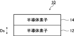
- FIG. 1 is a schematic diagram showing an example of a bonded body produced by the method for producing a bonded body of the present invention.
- FIG. FIG. 2 is a schematic cross-sectional view showing an example of a semiconductor element used in the method for producing a bonded body of the present invention.
- 3 is a schematic cross-sectional view showing an example of a bonding step in the method for producing a bonded body of the present invention.
- FIG. FIG. 4 is a schematic cross-sectional view showing an example of a bonded body obtained by the bonding step shown in FIG. 3 .
- the “content” of the component means the total content of those two or more components.
- the temperature and pressure are within the tolerances generally accepted in the relevant technical field. Temperature is 23° C. unless otherwise specified in the specification.
- the term “same” includes a generally acceptable margin of error in the relevant technical field.
- the terms “all over” and “overall” include a generally acceptable margin of error in the relevant technical field.
- the manufacturing method of the bonded body according to the present invention includes a preparation step of preparing bonding members having a maximum surface height Rmax of 50 nm or less, a pretreatment step of bringing a treatment liquid into contact with the surface of the bonding member, and a bonding step of bonding the treated bonding member that has been subjected to the pretreatment step to another bonding member.
- the treatment liquid used in the pretreatment step of the present production method contains a reducing agent, and the content of a metal corrosion inhibitor contained in the treatment liquid is 0.01 mass % or less based on the total mass of the treatment liquid.
- a metal oxide film made of an oxide of a metal contained in the conductive portion may be formed on the exposed conductive portion. Since the metal oxide film is difficult to join to other members such as metal films, a process is performed to remove the metal oxide film from the surface of the joining member by wet etching or the like before joining. However, when a removal process by wet etching is applied to the metal oxide film, it is presumed that the surface roughness after the process increases, and as a result, the joining strength of the joined body obtained by joining to another joining member is reduced.
- the manufacturing method of the present invention is characterized in that a treatment liquid containing a reducing agent is brought into contact with the surface of a bonding member having a maximum height Rmax of 50 nm or less.
- a treatment liquid containing a reducing agent is brought into contact with the surface of a bonding member having a maximum height Rmax of 50 nm or less.
- the manufacturing method of the present invention is also characterized by using a treatment solution containing 0.01 mass % or less of a metal corrosion inhibitor, which is presumably used to suppress the amount of components that may inhibit bonding near the surface of the metal film, thereby obtaining a bonded body with improved bonding strength.
- a bonded body means a member in which at least two bonding members are electrically connected to each other and bonded in a conductive state.
- the term “joint member” refers to a member that constitutes a semiconductor device, and includes, for example, a semiconductor element that exerts a specific function by itself, but also includes a member that exerts a specific function when multiple elements are assembled.
- the term “joint member” also includes a member that has only the function of transmitting an electrical signal, such as a wiring member.
- the term “treated bonded member” refers to a bonded member that has been treated with the above-mentioned specific treatment liquid.
- bonded members at any stage, including treated bonded members may be simply referred to as "bonded members.”
- FIG. 1 is a schematic diagram showing an example of the structure of a bonded body produced by the present production method.
- the stacked device (jointed body) 10 shown in FIG. 1 is, for example, a component in which a semiconductor element 12 and a semiconductor element 14 are stacked and joined in a stacking direction Ds, and the semiconductor element 12 and the semiconductor element 14 are directly electrically connected to each other.
- a laminated device is an example of a bonded body formed by bonding at least two bonding members, and refers to a member that exerts a specific function by itself.
- FIG. 2 is a schematic cross-sectional view showing an example of the configuration of a semiconductor element, which is a type of bonding member.
- Each of the semiconductor elements (bonding members) 12 and 14 shown in FIG. 2 has a semiconductor layer 32, a redistribution layer 34, a passivation layer 36, and a plurality of terminals 30.
- the semiconductor layer 32 is a layer made of a semiconductor.
- the type of semiconductor that makes up the semiconductor layer 32 is not particularly limited, but examples thereof include silicon, silicon carbide, germanium, gallium arsenide, and gallium nitride.
- a plurality of terminals 30 are provided on a surface 32a of the semiconductor layer 32.
- a device region (not shown) in which a circuit or the like that performs a specific function is formed is provided on the surface 32a of the semiconductor layer 32.
- a semiconductor device and a semiconductor wafer have an element region.
- the element region is a region in which various element configuration circuits, such as a capacitor, resistor, and coil, are formed to function as an electronic element.
- the element region may be, for example, a region in which a memory circuit such as a flash memory, a logic circuit such as a microprocessor and an FPGA (field-programmable gate array), or a region in which a communication module such as a wireless tag and wiring are formed.
- a transmission circuit or a MEMS Micro Electro Mechanical Systems
- Examples of the MEMS include sensors, actuators, and antennas.
- the sensors include various sensors such as acceleration, sound, and light sensors.
- the rewiring layer 34 is an electrically insulating layer provided on the surface 32a of the semiconductor layer 32.
- An example of an insulating material constituting the rewiring layer 34 is polyimide.
- the redistribution layer 34 is provided with wiring 37 electrically connected to the element region of the semiconductor layer 32.
- the wiring 37 is provided with a pad 38, and the wiring 37 and the pad 38 are electrically connected to each other.
- the wiring 37 is not provided and only the pad 38 is provided.
- the wiring 37 and the pads 38 are members made of a conductive material, for example, copper, a copper alloy, aluminum, an aluminum alloy, or the like.
- the passivation layer 36 is an electrically insulating layer that is provided on the surface 34a of the redistribution layer 34.
- insulating materials that form the passivation layer 36 include silicon nitride (SiN) and polyimide.
- the passivation layer 36 is provided with a terminal 30a at a position where the wiring 37 and pad 38 of the redistribution layer 34 are provided.
- the terminal 30a is electrically connected to the element region via the wiring 37 and pad 38, and is capable of transmitting and receiving signals to and from the element region and supplying voltage and the like to the element region.
- a terminal 30b is provided in the passivation layer 36 at a position where only the pad 38 of the rewiring layer 34 is provided. Unlike the terminal 30a, this terminal 30b is not electrically connected to the semiconductor layer 32.
- the constituent material of terminals 30a and 30b is not particularly limited as long as it is a material that has electrical conductivity, like wiring 37 and pad 38. Examples include metals and alloys, and materials used for components called terminals or electrode pads in the semiconductor device field can also be used as appropriate.
- the surfaces of the semiconductor elements 12 and 14 have end faces 30c where the terminals 30a and 30b, which are conductive portions, are exposed, and end faces 36a where the passivation layer 36, which is an insulating portion, is exposed.
- the bonding member has a conductive portion containing metal and an insulating portion having electrical insulation properties.
- the bonding member has at least a surface on which the conductive portion containing metal and the insulating portion are exposed and has a maximum height Rmax of 50 nm or less.
- a treatment is performed by contacting the surface with a specific treatment liquid.
- Examples of metals and alloys constituting the conductive portion of the joining member include copper, copper alloys, aluminum, and aluminum alloys.
- the conductive portion is preferably made of copper or a copper alloy.
- the metal oxide film contains an oxide of copper or a copper alloy.
- the semiconductor elements used as bonding members in this manufacturing method are not limited to the semiconductor elements 12 and 14 shown in FIG. 2, but may be appropriately selected depending on the intended laminated device.
- the semiconductor element is not particularly limited, and examples thereof include logic LSIs (Large Scale Integration) (e.g., ASICs (Application Specific Integrated Circuits), FPGAs (Field Programmable Gate Arrays), ASSPs (Application Specific Standard Products), etc.), microprocessors (e.g., CPUs (Central Processing Units), GPUs (Graphics Processing Units), etc.), memories (e.g., DRAMs (Dynamic Random Access Memory), HMCs (Hybrid Memory Cubes), MRAMs (Magnetic RAMs) and PCMs (Phase-Change Memory), ReRAMs (Resistive RAMs), FeRAMs (Ferroelectric RAMs), flash memories (NAND (Not AND) flash), etc.), LEDs (Light Emitting Diodes), (e.g.
- a semiconductor element is, for example, a self-contained component that performs a specific function, such as a circuit or a sensor, by itself. The sizes and configurations of the multiple semiconductor elements to be bonded in
- This manufacturing method includes a preparation step of preparing a joining member having a surface (hereinafter also referred to as a "specific surface") on which a conductive portion and an insulating portion each containing a metal are exposed and whose maximum height Rmax is 50 nm or less.
- the preparation step may include, for example, a planarization step of planarizing the surfaces of the bonding members on which the conductive and insulating parts are exposed to form the specific surface.
- the preparation step may also include procuring the bonding members by purchasing or the like.
- the maximum height Rmax of the specific surface of the bonding member prepared by the preparation step is 50 nm or less. In terms of better bonding properties, the maximum height Rmax of the specific surface is preferably 10 nm or less, more preferably 5 nm or less. The lower limit of the maximum height Rmax is not particularly limited, and may be, for example, 0.1 nm or more.
- the maximum height Rmax (arithmetic mean height) of the surface of the joining members is determined in accordance with JIS B 0601 by measuring the maximum height at any five points on the surface of the joining members using an atomic force microscope and calculating the arithmetic mean of the obtained measured values.
- the surface roughness Ra of the specific surface of the joining member is not particularly limited, but is preferably 3 nm or less, more preferably 1 nm or less, in terms of better joining properties.
- the lower limit of the surface roughness Ra is not particularly limited, and may be, for example, 0.2 nm or more.
- the surface roughness Ra (arithmetic mean height) of the surface of the joining member is determined in accordance with JIS B 0601 by measuring the surface roughness at any five points on the surface of the joining member using an atomic force microscope and calculating the arithmetic mean of the obtained measured values.
- the contact angle of water in the surface region where the insulating portion is exposed (hereinafter also referred to as the "insulating surface region") among the specific surfaces of the joining member is preferably 35 degrees or less, more preferably 30 degrees or less, and even more preferably 25 degrees or less, in terms of superior joining properties.
- the lower limit is not particularly limited, and may be, for example, 5 degrees or more.
- Methods for adjusting the contact angle of the insulating surface region include, for example, selecting the constituent material of the insulating portion and controlling the surface roughness by planarization treatment.
- the contact angle of the insulating surface region with water is obtained by flattening the surface of a model system consisting of only the same constituent material as the insulating part of the joining member, and measuring the contact angle of the surface of the obtained model system by the sessile drop method. Specifically, water is dropped onto the exposed insulating surface region, and the angle between the insulating surface region and the water on the side containing the water is measured to obtain the contact angle.
- a method for determining the contact angle by the sessile drop method is described, for example, in "Wettability and Control” (published by Technical Information Association Co., Ltd. on Jan. 31, 2001).
- the contact angle of the droplet on the insulating surface region may be measured using a known measuring device, such as a fully automatic contact angle meter "DMo-901" (manufactured by Kyowa Interface Science Co., Ltd.).
- planarization process As a preparation step in the present manufacturing method, it is preferable to form a specific surface by a planarization step of planarizing the surface of the joining member.
- the planarization process can form a flat surface state in which end face 30c of terminal 30a, end face 30c of terminal 30b, and surface 36a of passivation layer 36 form the same plane, as shown in semiconductor elements 12 and 14 in FIG. 2.
- CMP chemical mechanical polishing
- polishing liquid polishing slurry
- abrasive particles abrasive grains
- Examples of CMP include, but are not limited to, the CMP process described in Journal of the Japan Society for Precision Engineering, Vol. 84, No. 3, 2018.
- the polishing liquid used in CMP is not particularly limited as long as it contains abrasive particles.
- CMP may also be performed using a polishing liquid that does not contain abrasive particles.
- the abrasive particles include inorganic abrasive particles such as silica, alumina, zirconia, ceria, titania, germania, and silicon carbide; and organic abrasive particles such as polystyrene, polyacrylic, and polyvinyl chloride.
- the polishing liquid preferably contains water and a metal corrosion inhibitor, and may also contain at least one additive selected from the group consisting of hydrogen peroxide, an organic solvent, a passivation film forming agent, and a surfactant.
- the polishing liquid is preferably a slurry containing abrasive particles.
- the polishing liquid used for CMP the polishing liquids described in the specification of International Publication No. 2018/159530 and the like can be used, the contents of which are incorporated herein by reference.
- a pretreatment step is performed in which a specific surface of the joining member prepared in the preparation step is brought into contact with a specific treatment liquid, which will be described later.
- a method for treating a bonded member which is another embodiment of the present invention is a method for treating a bonded member used for manufacturing a bonded body, in which a specific treatment liquid is brought into contact with a specific surface of the bonded member.
- the pretreatment step of this manufacturing method and the treatment method of the joining member will not be distinguished from each other.
- a treated joining member By subjecting the joining member to the above treatment, a treated joining member is obtained. By joining such a treated joining member to another joining member (preferably a similarly treated joining member), a joined body with improved joining strength is obtained. It is presumed that in the treated joining member, the metal oxide film formed on the conductive surface of the joining member is reduced by the treatment liquid, and a metal film with stronger joining strength is formed on a specific surface of the joining member.
- the treatment liquid used in the pretreatment step contains a reducing agent, and the content of a metal corrosion inhibitor contained in the treatment liquid is 0.01 mass % or less based on the total mass of the treatment liquid.
- a metal corrosion inhibitor contained in the treatment liquid is 0.01 mass % or less based on the total mass of the treatment liquid.
- the processing liquid contains a reducing agent.
- the reducing agent is not particularly limited as long as it is a compound having a reducing function, and examples thereof include inorganic acid reducing agents, organic acid reducing agents, and other reducing agents such as sugars.
- the inorganic acid reducing agent is a compound selected from inorganic acids having a reducing function and salts thereof.
- inorganic acid reducing agents include at least one compound selected from the group consisting of nitrous acid and its salts, sulfurous acid and its salts, and thiosulfuric acid and its salts. Among them, at least one selected from the group consisting of nitrous acid and its salts, and thiosulfuric acid and its salts is preferred, and thiosulfuric acid and its salts are more preferred in terms of superior bonding strength of the bonded body.
- the inorganic acid reducing agent is in the form of a salt
- the salt include sodium salts, potassium salts and ammonium salts.
- the organic acid reducing agent is a compound selected from organic acids having a reducing function, organic acid derivatives, and salts thereof.
- organic acid derivatives include esters of organic acids and alcohol compounds, ethers of organic acids having a hydroxyl group and alcohol compounds, and esters of organic acids having a hydroxyl group and inorganic acids such as phosphoric acid and sulfuric acid.
- the organic acid reducing agent is in the form of a salt
- examples of the salt include sodium salts, potassium salts and ammonium salts.
- the organic acid reducing agent includes at least one compound selected from the group consisting of ascorbic acid, formic acid, oxalic acid, and 3,4,5-trihydroxybenzoic acid, derivatives thereof, and salts thereof.
- Ascorbic acid includes L-ascorbic acid, D-ascorbic acid, and isoascorbic acid.
- the derivatives include ascorbic acid derivatives such as alkyl glyceryl ascorbic acid, glycerol ascorbate, alkyl ether ascorbate, alkyl ester ascorbate, ascorbic acid sulfate, and ascorbic acid phosphate.
- organic acid reducing agent at least one selected from the group consisting of ascorbic acid, formic acid, oxalic acid, 3,4,5-trihydroxybenzoic acid, and salts thereof is preferable, and formic acid is more preferable in that the bonding strength of the bonded body is superior.
- reducing agents other than inorganic acid-based reducing agents and organic acid-based reducing agents include sugars such as fructose, glucose, and ribose, hydrogen peroxide, reducing sulfur compounds, and hydrazine compounds such as hydrazine and hydrazide compounds.
- the reducing sulfur compound is a compound that contains a sulfur atom and functions as a reducing agent.
- Examples of the reducing sulfur compound include mercaptosuccinic acid, dithiodiglycerol, bis(2,3-dihydroxypropylthio)ethylene, sodium 3-(2,3-dihydroxypropylthio)-2-methyl-propylsulfonate, 1-thioglycerol, sodium 3-mercapto-1-propanesulfonate, 2-mercaptoethanol, thioglycolic acid, and 3-mercapto-1-propanol.
- the reducing agent is preferably at least one selected from the group consisting of inorganic acid reducing agents, organic acid reducing agents, and sugars, more preferably nitrous acid, sulfurous acid, thiosulfuric acid, ascorbic acid, formic acid, oxalic acid, 3,4,5-trihydroxybenzoic acid, glucose, derivatives thereof, and salts thereof, and even more preferably nitrite, thiosulfate, ascorbic acid, formic acid, oxalic acid, 3,4,5-trihydroxybenzoic acid, or glucose.
- the reducing agent may be used alone or in combination of two or more kinds.
- the content of the reducing agent is preferably 0.1 mass % or more, more preferably 0.5 mass % or more, and even more preferably 1.0 mass % or more, based on the total mass of the treatment liquid, in order to provide a more excellent bonding strength of the bonded body.
- the content of the reducing agent is preferably 10.0 mass % or less, and more preferably 5.0 mass % or less, based on the total mass of the treatment liquid, in order to provide a more excellent bonding strength of the bonded body.
- the treatment liquid may contain a metal corrosion inhibitor. However, when the treatment liquid contains a metal corrosion inhibitor, the content of the metal corrosion inhibitor is 0.01 mass % or less based on the total mass of the treatment liquid.
- the metal corrosion inhibitor is a compound that has the function of preventing corrosion of the metal components that constitute the conductive portion of the joint member to be treated.
- Metal corrosion inhibitors include, for example, heterocyclic compounds.
- heterocyclic compounds include azole compounds, pyrrole compounds, pyridine compounds, pyrazine compounds, pyrimidine compounds, indole compounds, indolizine compounds, indazole compounds, quinoline compounds, and oxazole compounds.
- a triazole compound, a tetrazole compound, or a pyrrole compound is preferable, and a triazole compound is more preferable.
- the azole compound includes its tautomers.
- Azole compounds include, for example, imidazole compounds in which one of the atoms constituting the azole ring is a nitrogen atom, pyrazole compounds in which two of the atoms constituting the azole ring are nitrogen atoms, thiazole compounds in which one of the atoms constituting the azole ring is a nitrogen atom and the other is a sulfur atom, triazole compounds in which three of the atoms constituting the azole ring are nitrogen atoms, and tetrazole compounds in which four of the atoms constituting the azole ring are nitrogen atoms, with triazole compounds and tetrazole compounds being preferred.
- the triazole compound includes a benzotriazole compound in which two adjacent substituents on a triazole ring are bonded to each other to form a benzene ring.
- benzotriazole compounds include benzotriazole, 5-methyl-1H-benzotriazole (CAS Registry Number: 136-85-6), tolyltriazole (CAS Registry Number: 29385-43-1), 5-aminobenzotriazole, 1-hydroxybenzotriazole, 4-carboxybenzotriazole, 5,6-dimethylbenzatriazole, 1-[N,N-bis(hydroxyethyl)aminoethyl]benzotriazole, 1-(1,2-dicarboxyethyl)benzotriazole, 1-[N,N-bis(2-ethylhexyl)aminomethyl]benzotriazole, 1-[N,N-bis(2-ethylhexyl)aminomethyl]methylbenzotriazole, 2,2'- ⁇ [(methyl
- triazole compounds other than benzotriazole compounds include 1,2,3-triazole, 1,2,4-triazole, 3-methyl-1,2,4-triazole, 3-amino-1,2,4-triazole, and 1-methyl-1,2,3-triazole.
- Tetrazole compounds include, for example, 1H-tetrazole (1,2,3,4-tetrazole), 5-methyl-1,2,3,4-tetrazole, 5-amino-1,2,3,4-tetrazole, 1,5-pentamethylenetetrazole, 1-phenyl-5-mercaptotetrazole, and 1-(2-dimethylaminoethyl)-5-mercaptotetrazole.
- the metal corrosion inhibitors may be used alone or in combination of two or more.
- the content of the metal corrosion inhibitor contained in the treatment liquid is preferably 0.01 mass % or less relative to the total mass of the treatment liquid, and it is preferable that the treatment liquid is substantially free of a metal corrosion inhibitor.
- the term "substantially free of" a certain component means that the content of that component is 0.001% by mass or less relative to the total mass of the treatment liquid.
- the treatment liquid may contain water, and preferably contains water.
- the type of water used in the treatment solution may be any type that does not adversely affect the semiconductor substrate, and may be distilled water, deionized (DI) water, or pure water (ultrapure water). Pure water (ultrapure water) is preferred because it contains almost no impurities and has less effect on the semiconductor substrate during the manufacturing process of the semiconductor substrate.
- the content of water may be the balance of the reducing agent, metal anticorrosive, antibacterial agent, and other components described later, and is preferably 85% by mass or more, more preferably 90% by mass or more, and even more preferably 95% by mass or more, based on the total mass of the treatment liquid.
- the upper limit is preferably 99.99% by mass or less, more preferably 99.9% by mass or less, and even more preferably 99% by mass or less, based on the total mass of the treatment liquid.
- the remainder excluding the reducing agent, the metal corrosion inhibitor, the optionally added antibacterial agent, and any unintentionally mixed impurities is water, and it is more preferable that the remainder excluding the reducing agent, the optionally added antibacterial agent, and any unintentionally mixed impurities is water.
- the treatment liquid may contain an antibacterial agent.
- the antibacterial agent is a compound that has an antibacterial effect against bacteria, and any compound that does not inhibit the reducing action of the treatment liquid can be used as appropriate.
- the antibacterial agent may be in the form of a salt (eg, a known salt, etc.).
- antibacterial agents examples include quaternary ammonium compounds, alcohol-based antibacterial agents, phenol-based antibacterial agents, aldehyde-based antibacterial agents, carboxylic acid-based antibacterial agents, ester-based antibacterial agents, ether-based antibacterial agents, nitrile-based antibacterial agents, peroxide-based antibacterial agents, halogen-based antibacterial agents, pyridine-based antibacterial agents, triazine-based antibacterial agents, isothiazolin-based antibacterial agents, imidazole-based antibacterial agents, anilide-based antibacterial agents, piguanide-based antibacterial agents, disulfide-based antibacterial agents, thiocarbamate-based antibacterial agents, carbohydrate-based antibacterial agents, tropolone-based antibacterial agents, surfactant-based antibacterial agents, and organometallic compounds.
- quaternary ammonium compounds phenol-based antibacterial agents, carboxylic acid-based antibacterial agents, isothiazolin-based antibacterial agents, and biguanide-based antibacterial agents are preferred, and quaternary ammonium compounds are more preferred.
- the quaternary ammonium compound includes a compound having at least one quaternary ammonium cationic group in the molecule, or a salt thereof, and having a bactericidal action.
- salts with anions containing halogen atoms, such as halide ions are preferred, and quaternary ammonium chloride, quaternary ammonium fluoride, or quaternary ammonium bromide are more preferred.
- the quaternary ammonium compound include salts of the above anions and a quaternary ammonium cation selected from the group consisting of tetramethylammonium cation, tetraethylammonium cation, tetrapropylammonium cation, tetrabutylammonium cation, methyltripropylammonium cation, methyltributylammonium cation, ethyltrimethylammonium cation, dimethyldiethylammonium cation, benzyltrimethylammonium cation, hexadecyltrimethylammonium cation, (2-hydroxyethyl)trimethylammonium cation, and spiro-(1,1')-bipyrrolidinium cation.
- a quaternary ammonium cation selected from the group consisting of tetramethylammonium cation, tetraeth
- quaternary ammonium compounds include benzalkonium chloride, didecyldimethylammonium chloride (DDAC), hexadecylpyridinium chloride (CPC), 3,3'-(2,7-dioxaoctane)bis(1-dodecylpyridinium bromide) (Hygeria), benzethonium chloride, and domiphen bromide.
- a salt of a cation selected from the group consisting of tetramethylammonium cation, tetraethylammonium cation, and tetrapropylammonium cation and an anion selected from the group consisting of chloride ion, fluoride ion, and bromide ion is preferred, and tetramethylammonium bromide, tetraethylammonium bromide, or tetrapropylammonium bromide is more preferred.
- Phenolic antimicrobial agents include, for example, cresol, chlorothymol, dichloroxylenol, and hexachlorophene.
- Carboxylic acid antibacterial agents include, for example, unsaturated carboxylic acids such as sorbic acid, and aromatic carboxylic acids such as benzoic acid and salicylic acid, with sorbic acid, benzoic acid, or salicylic acid being preferred.
- isothiazoline antibacterial agents include 5-chloro-2-methyl-4-isothiazolin-3-one and 2-methyl-4-isothiazolin-3-one.
- biguanide antibacterial agents include 1,1'-hexamethylenebis[5-(p-chlorophenyl)biguanide] dihydrochloride (chlorhexidine hydrochloride), bis(p-chlorophenyldiguanide)hexane digluconate (chlorhexidine gluconate), and poly(hexamethylene biguanide) hydrochloride (hexamethylene biguanide hydrochloride).
- the antibacterial agent may be used alone or in combination of two or more kinds.
- the content of the antibacterial agent is preferably from 0.01 to 0.1% by mass, and more preferably from 0.02 to 0.08% by mass, based on the total mass of the treatment liquid.
- the treatment liquid may contain other components in addition to the reducing agent, metal anticorrosive agent, water, and antibacterial agent, such as a surfactant, a pH adjuster, a complexing agent, and an organic solvent.
- the content of components other than the reducing agent, metal corrosion inhibitor, water, and antibacterial agent in the treatment liquid is preferably 10 mass % or less relative to the total mass of the treatment liquid, and it is more preferable that the treatment liquid is substantially free of components other than the reducing agent, metal corrosion inhibitor, water, and antibacterial agent.
- the content of components other than the reducing agent, water, and antibacterial agent in the treatment liquid is preferably 5 mass % or less relative to the total mass of the treatment liquid, and it is more preferable that the treatment liquid is substantially free of components other than the reducing agent, water, and antibacterial agent.
- the other components will be described below.
- a surfactant is a compound having a hydrophilic group and a hydrophobic group (lipophilic group) in one molecule.
- examples of surfactants include nonionic surfactants, anionic surfactants, cationic surfactants, and amphoteric surfactants.
- the surfactant is a compound different from the metal corrosion inhibitor.
- the surfactant often has at least one hydrophobic group selected from the group consisting of an aliphatic hydrocarbon group, an aromatic hydrocarbon group, and a combination thereof.
- the hydrophobic group contains an aromatic hydrocarbon group
- the number of carbon atoms in the hydrophobic group of the surfactant is preferably 6 or more, and more preferably 10 or more.
- the total number of carbon atoms in the surfactant is preferably 16 to 100.
- the surfactant for example, the compounds exemplified in paragraph [0126] of WO 2022/044893 can be used, the contents of which are incorporated herein by reference.
- the treatment solution may contain a pH adjuster to adjust and maintain the pH of the treatment solution.
- the pH adjuster is a basic compound or an acidic compound that is different from the above-mentioned components that may be contained in the treatment liquid, however, it is permissible to adjust the pH of the treatment liquid by adjusting the amount of each of the above-mentioned components added.
- a basic compound is a compound that exhibits alkaline properties (pH greater than 7.0) in an aqueous solution.
- the basic compound includes basic inorganic compounds, for example, alkali metal hydroxides such as sodium hydroxide and potassium hydroxide, and alkaline earth metal hydroxides.
- An acidic compound is a compound that exhibits acidity (pH less than 7.0) in an aqueous solution.
- the acidic compound includes inorganic acids having no reducing function, such as hydrochloric acid, sulfuric acid, sulfurous acid, and boric acid.
- the content of each of the above components in the treatment liquid can be measured by known methods such as gas chromatography-mass spectrometry (GC-MS), liquid chromatography-mass spectrometry (LC-MS), and ion-exchange chromatography (IC).
- GC-MS gas chromatography-mass spectrometry
- LC-MS liquid chromatography-mass spectrometry
- IC ion-exchange chromatography
- the treatment liquid may be either alkaline or acidic.
- the pH of the treatment liquid is preferably from 5 to 9, and more preferably from 6 to 8.
- the pH of the treatment solution can be measured by a method conforming to JIS Z8802-1984 using a known pH meter. The pH is measured at a temperature of 25°C.
- the treatment liquid can be prepared, for example, by mixing the above-mentioned components.
- the method for preparing the treatment liquid includes, for example, adding a reducing agent and, if necessary, optional components such as an antibacterial agent and a metal corrosion inhibitor to a container containing purified pure water, and then stirring and mixing to prepare the treatment liquid.
- a reducing agent and, if necessary, optional components such as an antibacterial agent and a metal corrosion inhibitor
- a container containing purified pure water and then stirring and mixing to prepare the treatment liquid.
- each component to the container they may be added all at once, or may be added in multiple portions. The order in which each component is added can be appropriately selected.
- the stirring device and stirring method used to prepare the treatment liquid may be a device known as a stirrer or disperser.
- stirrers include industrial mixers, portable stirrers, mechanical stirrers, and magnetic stirrers.
- dispersers include industrial dispersers, homogenizers, ultrasonic dispersers, and bead mills.
- the mixing of the components in the preparation process of the treatment liquid, the purification process described below, and the storage of the produced treatment liquid are preferably carried out at 5 to 40°C.
- the degree of purification is preferably such that the purity of the raw material is 99% by mass or more, and more preferably such that the purity of the undiluted solution is 99.9% by mass or more.
- the upper limit is, for example, 99.9999% by mass or less.
- purification methods include passing the raw material through an ion exchange resin or a reverse osmosis membrane (RO membrane), distilling the raw material, and filtering.
- the purification process may be a combination of the above purification methods.
- the raw material may be subjected to a primary purification process in which the raw material is passed through an RO membrane, and then a secondary purification process in which the raw material is passed through a purification device made of a cation exchange resin, an anion exchange resin, or a mixed-bed ion exchange resin.
- the purification process may be carried out multiple times.
- the filter used for filtering is not particularly limited as long as it is a filter that has been conventionally used for filtering purposes, etc.
- filters made of fluororesins such as polytetrafluoroethylene (PTFE) and tetrafluoroethylene perfluoroalkyl vinyl ether copolymer (PFA), polyamide resins such as nylon, polyarylsulfone (PAS), and polyolefin resins (including high density or ultra-high molecular weight) such as polyethylene and polypropylene (PP).
- fluororesins such as polytetrafluoroethylene (PTFE) and tetrafluoroethylene perfluoroalkyl vinyl ether copolymer (PFA)
- polyamide resins such as nylon
- PAS polyarylsulfone
- PP polypropylene
- the treatment liquid used in the pretreatment step may be a diluted liquid obtained by diluting a stock solution containing at least a reducing agent before use.
- the dilution rate of the stock solution may be appropriately adjusted depending on the type and content of the components contained in the stock solution.
- the ratio of the treatment liquid (diluted liquid) to the stock solution is preferably 10 to 1000 times, more preferably 15 to 500 times, and even more preferably 20 to 100 times, in volume ratio.
- the dilution treatment it is preferable to dilute the stock solution with water. It is preferable to perform a purification treatment in advance on the water used in the dilution treatment.
- the purification treatment is not particularly limited, and examples thereof include the ion component reduction treatment using an ion exchange resin or an RO membrane, etc., and the removal of foreign matter using filtering, which are described above as purification treatments for the treatment liquid, and it is preferable to perform any one of these treatments.
- the content of the metal corrosion inhibitor in the undiluted stock solution is not particularly limited as long as the content of the metal corrosion inhibitor in the diluted cleaning solution is 0.01 mass% or less, and may be, for example, 0.1 mass% or less relative to the total mass of the stock solution, and preferably 0.01 mass% or less.
- the lower limit is not particularly limited, and it is preferable that the stock solution does not substantially contain the metal corrosion inhibitor.
- the content of the reducing agent in the stock solution is not particularly limited, but is preferably 0.1 to 5 mass %, more preferably 0.2 to 2 mass %, based on the total mass of the stock solution.
- the content of the antibacterial agent in the stock solution is preferably 0.1 to 5 mass %, more preferably 0.2 to 2 mass %, based on the total mass of the stock solution.
- the content of components other than the reducing agent, metal corrosion inhibitor, water and antibacterial agent in the original solution is preferably 10 mass% or less based on the total mass of the original solution, and it is more preferable that the original solution does not substantially contain components other than the reducing agent, metal corrosion inhibitor, water and antibacterial agent.
- the pH of the stock solution at 25° C. is preferably 5 to 9, and more preferably 6 to 8.
- the change in pH before and after dilution is preferably 1.0 or less, more preferably 0.5 or less.
- the specific method for diluting the stock solution is not particularly limited, and may be carried out in accordance with the above-mentioned method for preparing the treatment solution.
- the stirring device and stirring method used in the dilution process are also not particularly limited, and may be carried out using any of the known stirring devices listed in the above-mentioned method for preparing the treatment solution.
- the processing solution and the undiluted stock solution can be filled in any container for storage, transport and use, as long as corrosiveness and other issues do not pose a problem.
- a container with a high degree of cleanliness within the container for semiconductor applications and with suppressed elution of impurities from the inner wall of the container's storage section into each liquid is preferred.
- Examples of such containers include various containers commercially available as containers for semiconductor processing liquids, such as, but not limited to, the "Clean Bottle” series manufactured by Aicello Chemical Co., Ltd. and the "Pure Bottle” manufactured by Kodama Resin Industry Co., Ltd.
- the containers exemplified in paragraphs [0121] to [0124] of WO 2022/004217 can also be used, the contents of which are incorporated herein by reference.
- the method of pretreatment using the treatment liquid is not particularly limited as long as it is a method that brings a specific surface of the object to be joined, that is, the member to be joined, into contact with the treatment liquid, and can be carried out by any known method.
- methods for contacting the specific surface of the joined members with the treatment liquid include a method of immersing the joined members in the treatment liquid contained in a container for a certain period of time, a method of continuously supplying the treatment liquid to the specific surface of the joined members using a discharge nozzle, and a combination of these.
- the type of the discharge nozzle used to supply the treatment liquid is not particularly limited, and examples thereof include a straight nozzle, a shower nozzle, and a spray nozzle.
- the treatment liquid may be applied to the joining members while rotating them.
- the pretreatment by immersion it is preferable to perform ultrasonic treatment on the joining members immersed in the treatment liquid.
- the temperature of the treatment liquid used in the pretreatment step is not particularly limited, but is preferably from 10 to 60°C, and more preferably from 15 to 50°C.
- the contact time between the bonding member and the treatment liquid can be appropriately changed depending on the type and content of each component contained in the treatment liquid, but in practice, it is preferably 10 to 120 seconds, and more preferably 20 to 90 seconds.
- the supply amount (supply rate) of the treatment liquid when it is discharged is preferably from 50 to 5,000 mL/min, and more preferably from 200 to 2,000 mL/min.
- the contact between the joining member and the treatment liquid in the pretreatment step may be carried out only once, or may be carried out two or more times. When contacting two or more times, the same method may be repeated, or different methods may be combined.
- a drying treatment may be performed to dry the bonded members.
- the drying method include a spin drying method, a method of applying a dry gas to a specific surface of the joining members, a method of heating the joining members with a heating means such as a hot plate or an infrared lamp, and any combination of these methods.
- the treated bonded member obtained by carrying out the pretreatment step is subjected to the bonding step without being subjected to any other steps.
- the treated bonded members are preferably stored and transported under an atmosphere of an inert gas such as nitrogen, or under a reduced pressure atmosphere including a vacuum.
- the bonding process is a process of bonding a treated bonding member that has been subjected to a pretreatment process to another bonding member, and the bonding member that has been subjected to a pretreatment process is bonded to another bonding member.
- the bonding process provides a bonded body in which the two bonding members are fixed together while ensuring electrical connection between them.
- a treated joining member and a joining member that has not been subjected to a pretreatment step may be joined, but it is preferable that treated joining members are joined together. That is, it is preferable that the joined body is a member formed by joining treated joining members together.
- FIG. 3 is a schematic cross-sectional view showing an example of the bonding step in the present manufacturing method
- FIG. 4 is a schematic cross-sectional view showing an example of a bonded body obtained by the bonding step shown in FIG.
- the same components as those in the stacked device 10 and the semiconductor element 12 or 14 shown in Fig. 1 or Fig. 2 are denoted by the same reference numerals, and detailed description thereof will be omitted.
- the semiconductor elements 12 and 14 shown in Fig. 3 and Fig. 4 are treated bonding members that have been subjected to a pretreatment process.
- the semiconductor elements 12 and 14 are arranged so that their terminals 30 face each other. More specifically, the positions of the terminals 30a and 30b of the semiconductor elements 12 and 14 are aligned by using alignment marks (not shown) provided on the semiconductor elements 12 and 14, respectively. The process of aligning the positions of the semiconductor elements described above is also called alignment. After alignment, while maintaining the aligned state, the semiconductor element 12 and the semiconductor element 14 are brought close to each other and brought into contact with each other.
- the semiconductor element 12 and the semiconductor element 14 are bonded together to obtain the stacked device 10 shown in FIG.
- the terminals 30a corresponding to each other are directly connected to each other and the terminals 30b corresponding to each other are directly connected to each other through the above-mentioned bonding process.
- the semiconductor element 12 and the semiconductor element 14 are electrically and physically connected to each other through the respective terminals 30a. Note that the semiconductor element 12 and the semiconductor element 14 are not electrically connected to each other through the terminals 30b.
- the two bonding members are bonded under predetermined bonding conditions.
- the conditions in the bonding process such as the atmosphere, heating temperature, pressure (load), and processing time, can be appropriately selected depending on the device, such as a semiconductor element, that uses the bonded body to be manufactured.
- the temperature conditions in the bonding step are not particularly limited, but are preferably 150 to 350°C, and more preferably 200 to 300°C.
- the pressure conditions in the joining step are not particularly limited, but are preferably 30 MPa or less, and more preferably 0.1 to 20 MPa.
- the time for the bonding step is not particularly limited, but is preferably from 1 second to 60 minutes, and more preferably from 5 seconds to 10 minutes.
- the atmosphere for the bonding step can be selected from among air, an inert atmosphere such as a nitrogen atmosphere, and a reduced pressure atmosphere including a vacuum atmosphere.
- the heating temperature is not particularly limited to the above-mentioned temperature range, and can be selected from various temperatures in the range of 100 to 400°C.
- the heating rate can also be appropriately selected within the range of 10°C/min to 10°C/sec, depending on the performance of the heating stage or the heating method.
- the pressure (load) is not particularly limited to the above range either, and pressure conditions such as rapid pressure application or stepwise pressure application can be appropriately selected depending on the physical properties such as the strength of the objects to be joined.
- the atmosphere, the holding time of each of heating and pressurization in the bonding process, and the change time can be set as appropriate.
- the order of these steps can also be changed as appropriate.
- a procedure can be set in which, after a vacuum state is achieved, a first stage of pressurization is performed, and then, after heating and raising the temperature, a second stage of pressurization is performed, the pressure is held for a certain period of time, and the load is removed and simultaneously cooled, and when the temperature drops below a certain level, the atmosphere is returned to.
- Such a procedure can be rearranged in various ways. After pressurization under atmospheric pressure, heating can be performed under a vacuum, or evacuation, pressurization and heating can be performed simultaneously.
- a mechanism for individually controlling the pressure distribution and the heat distribution within the surface may be used, and the use of such a mechanism can improve the yield of the bonded body.
- the joining, transportation, and picking of the joining members (semiconductor elements) during the joining process can be achieved using known semiconductor manufacturing equipment.
- the present manufacturing method may include steps other than the preparation step, the pretreatment step, and the bonding step.
- the other steps include a cleaning step of cleaning a specific surface of the bonding member, and a singulation step of singulating a semiconductor element having a plurality of element regions into individual element regions.
- the cleaning step may be, for example, a method in which a specific surface of the joining member is cleaned with a cleaning liquid different from the treatment liquid used in the pretreatment step.
- impurities such as metal wiring and barrier metal removed in the planarization step, and abrasive particles (silica and alumina) used in the planarization step may remain on the specific surface of the bonding member. These impurities may cause short circuits between wirings, deteriorating the electrical properties of the bonding member.
- the above-mentioned impurities can be removed from the specific surface of the bonding member by performing a cleaning step on the bonding member that has been subjected to a planarization step such as CMP.
- the cleaning liquid used in the cleaning step is not particularly limited as long as it is a known cleaning liquid for semiconductor substrates that have been subjected to CMP treatment (pCMP cleaning liquid), has a different composition and action from the treatment liquid used in the pretreatment step, and is capable of removing or dissolving the above-mentioned impurities.
- the cleaning liquid the cleaning liquid described in JP-A-2007-269918 and the like can be used, the contents of which are incorporated herein by reference.
- the method for cleaning the specific surface of the bonded member with the cleaning liquid is not particularly limited as long as it is a method that brings the specific surface of the bonded member into contact with the cleaning liquid, and can be carried out by a known method.
- the method of contacting the specific surface of the joined members with the cleaning liquid includes the methods mentioned as the method of contacting the specific surface of the joined members with the treatment liquid in the pretreatment step, including the preferred embodiment.
- the specific surface of the joined members may also be cleaned by scrubbing, in which a cleaning member such as a brush is physically brought into contact with the specific surface of the joined members while a cleaning liquid is being supplied.
- the temperature of the washing solution used in the washing step is not particularly limited, but is preferably 10 to 60°C, more preferably 15 to 50°C.
- the contact time between the bonding member and the cleaning liquid can be appropriately changed depending on the type and content of each component contained in the cleaning liquid, but in practice, it is preferably 10 to 120 seconds, and more preferably 20 to 90 seconds.
- the supply amount (supply rate) is preferably 50 to 5000 mL/min, and more preferably 200 to 2000 mL/min.
- a rinsing process may be performed in which the bonded members are brought into contact with a rinsing liquid.
- the rinsing process is a process of rinsing a specific surface of the bonding member with a rinsing liquid, and is preferably performed consecutively after the above-mentioned cleaning.
- the rinsing process may be performed using the above-mentioned mechanical stirring method.
- rinsing liquids examples include water (preferably deionized water), methanol, ethanol, isopropyl alcohol (IPA), N-methylpyrrolidinone, ⁇ -butyrolactone, dimethyl sulfoxide, ethyl lactate, and propylene glycol monomethyl ether acetate.
- the above-mentioned method for bringing the treating liquid into contact with the bonded members can be similarly applied.
- the contact time between the bonding member and the rinse liquid can be appropriately changed depending on the type and content of each component contained in the cleaning liquid, and is preferably 10 to 120 seconds, more preferably 20 to 90 seconds.
- the temperature of the rinse solution is preferably from 0 to 50°C, more preferably from 15 to 35°C.
- a drying process may be performed to dry the bonded members. As the drying process, the drying process performed in the pre-treatment step can be similarly applied.
- the time that elapses from the completion of the above-mentioned cleaning process (including the above-mentioned rinsing process and drying process) for the joining member until the start of the pretreatment process is preferably 30 seconds or more, more preferably 1 minute or more, and even more preferably 2 minutes or more. This is because if the above-mentioned elapsed time is equal to or more than the above-mentioned lower limit, the semiconductor wafer can be easily transported. There is no particular upper limit, but from the viewpoint of shortening the manufacturing time, 30 minutes or less is preferable.
- the present manufacturing method may include a singulation step of singulating the bonding member into individual element regions.
- the singulation step can be carried out by a known method such as dicing or laser scribing.
- the singulation step may be performed, for example, after the preparation step or the cleaning step.
- the singulation step may be performed at any stage, such as before the pretreatment step, before the bonding step, or after the bonding step.
- the manufacturing method of the stacked device 10 shown in Figures 2 to 4 is a manufacturing method using a chip-on-chip system, but this manufacturing method may be a chip-on-wafer system in which a semiconductor element and a semiconductor wafer are used as joining members, or a wafer-on-wafer system in which two semiconductor wafers are used as joining members.
- An example of a semiconductor element used in the chip-on-wafer method is a semiconductor element having one element region and having at least two alignment marks on the surface indicating the position of the element region.
- an example of a semiconductor wafer used in the chip-on-wafer method is a semiconductor wafer having multiple element regions and having at least two alignment marks on the surface indicating the position of each element region.
- the above-mentioned preparation step, pretreatment step, and optional cleaning step are performed on the semiconductor element and the semiconductor wafer.
- the element region of the semiconductor element is bonded to the element region of the semiconductor wafer in accordance with the bonding process described above.
- the bonding may be performed by bonding a plurality of semiconductor elements together, or the semiconductor elements may be bonded to the semiconductor wafer one by one.
- the semiconductor wafer with the semiconductor elements bonded thereto is divided into individual element regions by, for example, dicing or laser scribing, etc. In this way, a plurality of stacked devices each having two semiconductor elements bonded thereto can be manufactured. By manufacturing a plurality of stacked devices at the same time as described above, the tact time can be reduced and the productivity can be improved.
- the stacked device manufactured by the present manufacturing method is not limited to the configuration shown in Fig. 1 or 4.
- the stacked device may have a configuration in which three or more semiconductor elements are stacked and joined in the stacking direction Ds, and adjacent semiconductor elements are directly and electrically connected to each other.
- the three or more semiconductor elements constituting the stacked device may have the same configuration or different configurations.
- the present manufacturing method can manufacture a stacked device using a semiconductor element provided with an element region in which an element configuration circuit and the like are formed and a rewiring layer. Therefore, examples of stacked devices manufactured by the present manufacturing method include a stacked device having a combination of a semiconductor element having a logic circuit and a semiconductor element having a memory circuit, a stacked device in which all semiconductor elements have memory circuits, and a stacked device in which all semiconductor elements have logic circuits, and all of these can be manufactured. Furthermore, the combination of semiconductor elements in the stacked device may be a combination of a sensor, an actuator, an antenna, or the like, with a memory circuit and a logic circuit, and is appropriately determined depending on the application of the stacked device, etc.
- the laminated device manufactured by the present manufacturing method may be a member that functions as an optical sensor.
- An example of a laminated device that functions as an optical sensor is a laminate in which a semiconductor element and a sensor chip provided with a lens are laminated in the stacking direction Ds.
- the configuration of the semiconductor element is not particularly limited as long as it has a logic circuit that can process a signal obtained by the sensor chip.
- the sensor chip has a light sensor that detects light.
- the light sensor is not particularly limited as long as it can detect light, and for example, a charge coupled device (CCD) image sensor or a complementary metal oxide semiconductor (CMOS) image sensor is used.
- the lens is not particularly limited in configuration as long as it can focus light on the sensor chip, and for example, a member called a microlens is used.
- Treatment solutions 2 to 10 and treatment solutions C1 and C2 having the compositions shown in Table 1 were prepared according to the above method, except that the types and amounts of each component were changed so as to obtain the compositions shown in Table 1.
- Example 1 (Preparation of joining materials) A Ta film having a thickness of 20 nm was formed on the surface of a silicon wafer having a diameter of 8 inches by a sputtering method. Subsequently, a copper film having a thickness of 50 nm was formed on the Ta film by a sputtering method, and then a copper film having a total thickness of 1000 nm was formed by a plating method, thereby producing a silicon wafer for evaluation having a Ta film and a copper film in this order on the silicon wafer.
- a planarization process was performed by polishing the copper film on the silicon wafer using a Kemet Corporation "ARW-681MSII” polishing device while supplying the slurry under the following conditions: .
- ⁇ Target substrate silicon wafer with Ta film and copper film
- ⁇ Table rotation speed 104 rpm
- Head rotation speed 105 rpm
- Polishing pressure 6.9 kPa
- the metal polishing liquid described in Example 1 of JP 2009-260304 A was used as the slurry.
- the slurry was prepared by mixing the following: The following components were added in the amounts required for the desired contents, then mixed and stirred, and the pH was adjusted to 6.0 with ammonia gas to prepare the solution.
- Colloidal silica manufactured by Fuso Chemical Co., Ltd.: PL-2H
- Metal corrosion inhibitor (1-(1,2-dicarboxyethyl)benzothiazole): 0.050% by mass
- Surfactant polyoxyethylene alkyl ether
- 0.1% by mass Hydrogen peroxide solution 1.0% by mass Glycine: 1.0% by mass
- the maximum height of the surface was measured using an atomic microscope in accordance with JIS B 0601. The measured values obtained were arithmetically averaged to determine the maximum height Rmax of the surface where the conductive portion subjected to the planarization process was exposed, and the maximum height Rmax was 4 nm. Furthermore, the surface roughness was measured at any five points on the surface of the copper film planarized by the above planarization process using an atomic microscope in accordance with JIS B 0601. The measured values obtained were arithmetically averaged to determine the surface roughness Ra of the surface where the conductive portion that had been subjected to the planarization process was exposed. As a result, the surface roughness Ra was 1 nm.
- a cleaning solution to be used in the cleaning step was prepared according to the method described in Example 1 of JP 2007-269918 A.
- the planarized silicon wafer was scrubbed for 25 seconds by supplying the diluted cleaning solution while contacting the surface of the silicon wafer with a PVA roll brush connected to a scrubbing unit built into a Kemet wafer cleaner "ZAB-8S1M-ODW.”
- the supply rate of the diluted cleaning solution to the planarized surface was 650 mL/min.
- the supply rate of the diluted cleaning solution to the surface of the silicon wafer opposite to the planarized surface was 500 mL/min.
- the silicon wafer was rinsed for 35 seconds with pure water (deionized water), which was supplied to the planarized surface of the silicon wafer at a rate of 650 mL/min and to the surface opposite to the planarized surface of the silicon wafer at a rate of 500 mL/min. Furthermore, the silicon wafer was dried for 30 seconds using a spin dry device built into the apparatus.
- pure water deionized water
- Pretreatment process A photolithography device (manufactured by Takizawa Sangyo Co., Ltd., product name "ED-3000”) was prepared, in which a straight nozzle (manufactured by Ikeuchi Co., Ltd., product name "CCP") was connected to a discharge port.
- the silicon wafer was placed in this device, and while rotating the silicon wafer at 300 rpm, treatment liquid 1 was discharged from the straight nozzle onto the planarized surface of the silicon wafer, thereby performing a pretreatment step, and a treated wafer was obtained.
- the discharge speed of treatment liquid 1 from the straight nozzle was 450 ml/min, and the time for which treatment liquid 1 was supplied was 1 minute.
- the cleaning step the time from the end of the drying process to the start of the pretreatment process was one minute.
- the treated wafer obtained by the pretreatment step described above was diced to prepare a first sample cut into a size of 10 mm square and a second sample cut into a size of 4 mm square.
- a bonding device (“FC-3000" manufactured by Toray Engineering Co., Ltd.)
- the first sample and the second sample were placed below and above, respectively, so that the surfaces that had been subjected to the pretreatment process faced each other, and a bonding process was performed by heating and pressing for 10 minutes under conditions of a load of 800 N and a temperature of 250°C. Thereafter, an annealing treatment was performed in an oven at 300°C for 2 hours in a nitrogen atmosphere, and a bonded body of Example 1 was obtained.
- Example 2 A pretreatment step was performed under the same conditions as in Example 1, except that a spray nozzle (manufactured by IKEUCHI CO., LTD., product name "VP") was connected to the outlet of the photolithography device instead of the straight nozzle, to obtain a bonded body of Example 2.
- a spray nozzle manufactured by IKEUCHI CO., LTD., product name "VP"
- Examples 3 to 11, Comparative Example 1, Comparative Example 2 The joint members of Examples 3 to 11 and Comparative Examples 1 and 2 were each manufactured according to the method of Example 1, except that the pretreatment step was carried out using the treatment liquid shown in Table 1.
- Examples 1 to 11 had superior bonding strengths for the resulting joints compared to Comparative Example 1, in which the pretreatment process was carried out using a treatment solution that did not contain a reducing agent, and Comparative Example 2, in which the pretreatment process was carried out using a treatment solution that contained 0.1 mass% of a metal corrosion inhibitor relative to the total mass of the treatment solution.
- Laminated device (joint) 12 14 Semiconductor element (joining member) 30, 30a, 30b Terminal 30c End surface 32 Semiconductor layer 32a, 34a, 36a Surface 34 Redistribution layer 36 Passivation layer 37 Wiring 38 Pad Ds Stacking direction
Landscapes
- Engineering & Computer Science (AREA)
- Manufacturing & Machinery (AREA)
- Pressure Welding/Diffusion-Bonding (AREA)
- Preventing Corrosion Or Incrustation Of Metals (AREA)
- Adhesives Or Adhesive Processes (AREA)
- Die Bonding (AREA)
Priority Applications (3)
| Application Number | Priority Date | Filing Date | Title |
|---|---|---|---|
| CN202480014996.3A CN120814039A (zh) | 2023-03-30 | 2024-02-29 | 接合体的制造方法、处理液及处理方法 |
| KR1020257027758A KR102957547B1 (ko) | 2023-03-30 | 2024-02-29 | 접합체의 제조 방법, 처리액 및 처리 방법 |
| JP2025510055A JPWO2024202901A1 (https=) | 2023-03-30 | 2024-02-29 |
Applications Claiming Priority (2)
| Application Number | Priority Date | Filing Date | Title |
|---|---|---|---|
| JP2023-055033 | 2023-03-30 | ||
| JP2023055033 | 2023-03-30 |
Publications (1)
| Publication Number | Publication Date |
|---|---|
| WO2024202901A1 true WO2024202901A1 (ja) | 2024-10-03 |
Family
ID=92905381
Family Applications (1)
| Application Number | Title | Priority Date | Filing Date |
|---|---|---|---|
| PCT/JP2024/007535 Ceased WO2024202901A1 (ja) | 2023-03-30 | 2024-02-29 | 接合体の製造方法、処理液および処理方法 |
Country Status (4)
| Country | Link |
|---|---|
| JP (1) | JPWO2024202901A1 (https=) |
| CN (1) | CN120814039A (https=) |
| TW (1) | TW202505653A (https=) |
| WO (1) | WO2024202901A1 (https=) |
Citations (5)
| Publication number | Priority date | Publication date | Assignee | Title |
|---|---|---|---|---|
| JP2013038112A (ja) * | 2011-08-04 | 2013-02-21 | Sony Corp | 半導体装置、半導体装置の製造方法、及び、電子機器 |
| WO2018159186A1 (ja) * | 2017-02-28 | 2018-09-07 | 富士フイルム株式会社 | 半導体デバイス、積層体ならびに半導体デバイスの製造方法および積層体の製造方法 |
| WO2022244717A1 (ja) * | 2021-05-17 | 2022-11-24 | 富士フイルム株式会社 | ポリイミド含有部形成用組成物、接合体の製造方法、接合体、デバイスの製造方法、及び、デバイス。 |
| JP7220796B2 (ja) * | 2019-08-16 | 2023-02-10 | 富士フイルム株式会社 | 構造体の製造方法 |
| JP2023177917A (ja) * | 2022-06-03 | 2023-12-14 | 三井化学株式会社 | 半導体装置およびその製造方法 |
-
2024
- 2024-02-29 JP JP2025510055A patent/JPWO2024202901A1/ja active Pending
- 2024-02-29 CN CN202480014996.3A patent/CN120814039A/zh active Pending
- 2024-02-29 WO PCT/JP2024/007535 patent/WO2024202901A1/ja not_active Ceased
- 2024-03-18 TW TW113109894A patent/TW202505653A/zh unknown
Patent Citations (5)
| Publication number | Priority date | Publication date | Assignee | Title |
|---|---|---|---|---|
| JP2013038112A (ja) * | 2011-08-04 | 2013-02-21 | Sony Corp | 半導体装置、半導体装置の製造方法、及び、電子機器 |
| WO2018159186A1 (ja) * | 2017-02-28 | 2018-09-07 | 富士フイルム株式会社 | 半導体デバイス、積層体ならびに半導体デバイスの製造方法および積層体の製造方法 |
| JP7220796B2 (ja) * | 2019-08-16 | 2023-02-10 | 富士フイルム株式会社 | 構造体の製造方法 |
| WO2022244717A1 (ja) * | 2021-05-17 | 2022-11-24 | 富士フイルム株式会社 | ポリイミド含有部形成用組成物、接合体の製造方法、接合体、デバイスの製造方法、及び、デバイス。 |
| JP2023177917A (ja) * | 2022-06-03 | 2023-12-14 | 三井化学株式会社 | 半導体装置およびその製造方法 |
Also Published As
| Publication number | Publication date |
|---|---|
| TW202505653A (zh) | 2025-02-01 |
| JPWO2024202901A1 (https=) | 2024-10-03 |
| CN120814039A (zh) | 2025-10-17 |
| KR20250137676A (ko) | 2025-09-18 |
Similar Documents
| Publication | Publication Date | Title |
|---|---|---|
| JP6808731B2 (ja) | 研磨液、化学的機械的研磨方法 | |
| EP1577934A1 (en) | Alkaline post-chemical mechanical planarization cleaning compositions | |
| KR20080016934A (ko) | 단일 플래튼 처리를 위한 방법 및 일체형 화학적 기계적연마 조성물 | |
| EP3394234B1 (en) | Composition for post chemical-mechanical-polishing cleaning | |
| US10947414B2 (en) | Compositions for use in chemical mechanical polishing | |
| WO2023181739A1 (ja) | 組成物、半導体素子の製造方法 | |
| TWI611046B (zh) | 半導體基板的蝕刻方法、蝕刻液及半導體元件的製造方法以及蝕刻液套組 | |
| US8916473B2 (en) | Method for forming through-base wafer vias for fabrication of stacked devices | |
| KR102957547B1 (ko) | 접합체의 제조 방법, 처리액 및 처리 방법 | |
| WO2024202901A1 (ja) | 接合体の製造方法、処理液および処理方法 | |
| KR102888183B1 (ko) | 세정 조성물, 반도체 기판의 세정 방법, 반도체 소자의 제조 방법 | |
| CN110140196B (zh) | 清洗液组合物 | |
| CN106537564A (zh) | 密封组合物以及半导体装置的制造方法 | |
| US20040074517A1 (en) | Surfactants for chemical mechanical polishing | |
| TWI791384B (zh) | 洗淨組成物、半導體基板的洗淨方法、及半導體元件的製造方法 | |
| US20110237079A1 (en) | Method for exposing through-base wafer vias for fabrication of stacked devices | |
| US20220106499A1 (en) | Polishing liquid and chemical mechanical polishing method | |
| TWI922692B (zh) | 清洗組成物、半導體基板的清洗方法、半導體元件的製造方法 | |
| TW202532632A (zh) | 半導體基板用洗淨液、被對象物的洗淨方法、半導體元件的製造方法 | |
| CN117441226A (zh) | 清洗组合物、半导体基板的清洗方法、半导体元件的制造方法 | |
| WO2026074880A1 (ja) | 組成物、洗浄済み被処理物の製造方法、電子デバイスの製造方法 | |
| WO2025018401A1 (ja) | 洗浄液組成物 | |
| TW202440882A (zh) | 處理液、處理方法 | |
| JP2005294282A (ja) | ポストcmp保管及び洗浄用の界面活性剤 | |
| WO2025204631A1 (ja) | 薬液、半導体デバイスの製造方法 |
Legal Events
| Date | Code | Title | Description |
|---|---|---|---|
| 121 | Ep: the epo has been informed by wipo that ep was designated in this application |
Ref document number: 24779040 Country of ref document: EP Kind code of ref document: A1 |
|
| ENP | Entry into the national phase |
Ref document number: 2025510055 Country of ref document: JP Kind code of ref document: A Ref document number: 1020257027758 Country of ref document: KR Free format text: ST27 STATUS EVENT CODE: A-0-1-A10-A15-NAP-PA0105 (AS PROVIDED BY THE NATIONAL OFFICE) |
|
| WWE | Wipo information: entry into national phase |
Ref document number: 1020257027758 Country of ref document: KR Ref document number: 2025510055 Country of ref document: JP |
|
| WWE | Wipo information: entry into national phase |
Ref document number: 202480014996.3 Country of ref document: CN |
|
| WWP | Wipo information: published in national office |
Ref document number: 202480014996.3 Country of ref document: CN |
|
| NENP | Non-entry into the national phase |
Ref country code: DE |
|
| 122 | Ep: pct application non-entry in european phase |
Ref document number: 24779040 Country of ref document: EP Kind code of ref document: A1 |