WO2024202761A1 - 樹脂配線基板および伸縮性デバイス - Google Patents
樹脂配線基板および伸縮性デバイス Download PDFInfo
- Publication number
- WO2024202761A1 WO2024202761A1 PCT/JP2024/006522 JP2024006522W WO2024202761A1 WO 2024202761 A1 WO2024202761 A1 WO 2024202761A1 JP 2024006522 W JP2024006522 W JP 2024006522W WO 2024202761 A1 WO2024202761 A1 WO 2024202761A1
- Authority
- WO
- WIPO (PCT)
- Prior art keywords
- wiring
- resin
- base material
- elastic
- linear
- Prior art date
- Legal status (The legal status is an assumption and is not a legal conclusion. Google has not performed a legal analysis and makes no representation as to the accuracy of the status listed.)
- Ceased
Links
Images







Classifications
-
- H—ELECTRICITY
- H05—ELECTRIC TECHNIQUES NOT OTHERWISE PROVIDED FOR
- H05K—PRINTED CIRCUITS; CASINGS OR CONSTRUCTIONAL DETAILS OF ELECTRIC APPARATUS; MANUFACTURE OF ASSEMBLAGES OF ELECTRICAL COMPONENTS
- H05K1/00—Printed circuits
- H05K1/02—Details
-
- H—ELECTRICITY
- H10—SEMICONDUCTOR DEVICES; ELECTRIC SOLID-STATE DEVICES NOT OTHERWISE PROVIDED FOR
- H10W—GENERIC PACKAGES, INTERCONNECTIONS, CONNECTORS OR OTHER CONSTRUCTIONAL DETAILS OF DEVICES COVERED BY CLASS H10
- H10W70/00—Package substrates; Interposers; Redistribution layers [RDL]
- H10W70/60—Insulating or insulated package substrates; Interposers; Redistribution layers
-
- H—ELECTRICITY
- H10—SEMICONDUCTOR DEVICES; ELECTRIC SOLID-STATE DEVICES NOT OTHERWISE PROVIDED FOR
- H10W—GENERIC PACKAGES, INTERCONNECTIONS, CONNECTORS OR OTHER CONSTRUCTIONAL DETAILS OF DEVICES COVERED BY CLASS H10
- H10W70/00—Package substrates; Interposers; Redistribution layers [RDL]
- H10W70/60—Insulating or insulated package substrates; Interposers; Redistribution layers
- H10W70/67—Insulating or insulated package substrates; Interposers; Redistribution layers characterised by their insulating layers or insulating parts
- H10W70/69—Insulating materials thereof
Definitions
- the present invention relates to a resin wiring board and a stretchable device.
- This application claims priority based on Japanese Patent Application No. 2023-054529, filed on March 30, 2023, the contents of which are incorporated herein by reference.
- Wearable devices are attracting attention in a wide range of fields, including sports science and healthcare. It is preferable for a wearable device to be able to be worn without any stress. For this reason, it is desirable for the device to be stretchable so that it can be worn on the object to which it is attached. In this specification, devices that have such characteristics are referred to as stretchable devices, regardless of their application as wearable devices.
- Patent Document 1 describes an elastic wiring board that includes a conductor substrate having an elastic resin substrate with a tensile modulus of elasticity of 10 to 50 MPa and a conductor layer provided on the elastic resin substrate, the conductor layer forming a wiring pattern. Patent Document 1 also describes that the elastic resin substrate includes a cured product of a curable resin composition that contains a rubber component and a filler.
- Patent Document 2 describes a wiring sheet in which an electrical lead-out pattern including terminal portions and a conductive line pattern are provided on an elastic substrate. Patent Document 2 also describes a wiring sheet in which at least the portions where the ends of the electrical lead-out pattern and the ends of the line pattern are in contact are coated and fixed with resin.
- the present invention has been made in consideration of the above problems, and has an object to provide a resin wiring board that can be easily electrically connected to other devices, and a stretchable device including the same.
- the wiring pattern has linear wiring in a planar line-of-sight configuration having an exposed portion exposed from the first surface of the resin base material in a cross-sectional view.
- the wiring pattern has a linear stretchable wiring having stretchability arranged on the first surface of the resin base material,
- the resin wiring board according to [7] having a resin coating layer that covers a portion where the stretchable wiring and the linear wiring are in contact.
- a stretchable device comprising the resin wiring substrate according to any one of [1] to [8].
- An electronic component is disposed on the first surface of the resin base material, The stretchable device according to [9], wherein the electronic component and the stretchable wiring are electrically connected.
- the resin wiring board of the present invention has a resin base material and a wiring pattern, and the wiring pattern has linear wiring in a plan view line having an exposed portion exposed from a first surface of the resin base material in a cross-sectional view. Therefore, for example, by using a method of printing a conductive material on the first surface of the resin base material, wiring that is in contact with the exposed portion of the linear wiring and electrically connected to another device is formed, whereby electrical connection to another device can be easily made. Furthermore, since the stretchable device of the present invention includes the resin wiring board of the present invention, it can be easily electrically connected to other devices.
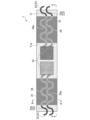
- FIG. 1 is a schematic diagram for explaining an example of a stretchable device of the present invention including a resin wiring board of the present invention.
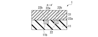
- 2 is a cross-sectional view of the stretchable device shown in FIG. 1 taken along line AA' shown in FIG. 1.
- 2 is a cross-sectional view of the stretchable device shown in FIG. 1 taken along line BB' shown in FIG. 1.
- 2A to 2C are process diagrams illustrating an example of a method for manufacturing the stretchable device shown in FIG. 1 .
- 2A to 2C are process diagrams illustrating an example of a method for manufacturing the stretchable device shown in FIG. 1 .
- 2A to 2C are process diagrams illustrating an example of a method for manufacturing the stretchable device shown in FIG. 1 .
- 2A to 2C are process diagrams illustrating an example of a method for manufacturing the stretchable device shown in FIG. 1 .
- 2A to 2C are process diagrams illustrating an example of a method for manufacturing the stretchable device shown in FIG. 1 .
- 2A to 2C are process diagrams illustrating an example of a method for manufacturing the stretchable device shown in FIG. 1 .
- 2A to 2C are process diagrams illustrating an example of a method for manufacturing the stretchable device shown in FIG. 1 .
- 2A to 2C are process diagrams illustrating an example of a method for manufacturing the stretchable device shown in FIG. 1 .
- FIG. 1 is a schematic plan view for explaining an example of a stretchable device of the present invention having a resin wiring board of the present invention.
- Fig. 2A is a cross-sectional view of the stretchable device shown in Fig. 1 cut along line A-A' shown in Fig. 1.
- Fig. 2B is a cross-sectional view of the stretchable device shown in Fig. 1 cut along line B-B' shown in Fig. 1.
- the stretchable device of this embodiment shown in Figures 1, 2A, and 2B includes a resin wiring board 1.
- the resin wiring board 1 has a resin base material 11 and a wiring pattern 21.
- the resin wiring board 1 and the resin base material 11 of this embodiment have a band-like shape.
- two electronic components 41 are disposed on a first surface 11a of the resin base material 11 disposed approximately at the center in the longitudinal direction of the resin wiring board 1.
- the resin substrate 11 is a sheet-like elastic resin substrate, and preferably has a breaking elongation rate of 50% or more, more preferably 200% or more.
- the resin substrate 11 is an elastic resin substrate with good elasticity having a breaking elongation rate of 50% or more
- the resin wiring board 1 can be suitably used for various stretchable devices such as wearable devices.
- the breaking elongation rate of the resin substrate 11 can be changed by appropriately selecting the material of the stretchable resin substrate.
- the breaking elongation rate of the resin substrate 11 is preferably 4000% or less. This is because the resin wiring board 1 is likely to have sufficient strength and durability.
- the "elongation at break” is defined as ⁇ (length at break - length before pulling) / length before pulling ⁇ x 100 (%).
- the elongation at break can be measured in each predetermined direction.
- “the elongation at break of the resin substrate 11 is 50% or more” refers to the elongation at break in the direction in which the elongation at break is the largest. If there is no anisotropy in the elongation at break, the elongation at break will be equal in any direction. If the anisotropy of the elongation at break is small, the elongation at break will be close in any direction.
- the metal substrate is clamped between the upper and lower grips of the measuring device, and the measurement sample is fixed to the metal substrate with double-sided tape so that the measurement point is 10 mm wide and 10 mm long.
- the measurement sample is then pulled at a pulling speed of 10 mm/min using a tensile tester (for example, product name: Autograph AGS-5kNX, manufactured by Shimadzu Corporation).
- the length of the measurement sample at the time of break is then measured, and the length before pulling (10 mm) is subtracted from this length to calculate the elongation at break for each measurement sample (length at break - length before pulling).
- the average value is taken as the elongation at break, and the breaking elongation percentage is calculated according to the above definition.
- the elastic resin substrate used as the resin substrate 11 may contain a resin having known elasticity.
- elastic resins include epoxy resins, urethane resins, urea resins, polyurethane urea resins, methacrylic acid resins, polyacrylic resins, silicone resins, diene resins, polyester resins, polyether resins, polyamide resins, and polystyrene resins.
- the elastic resin contained in the elastic resin substrate is a urethane resin
- the elastic resin substrate has a high breaking elongation and excellent flexibility, which is preferable.
- the elastic resin substrate used as the resin substrate 11 preferably does not contain a hardener. This is because the inclusion of a hardener does not promote deterioration of the elastic resin substrate over time, resulting in an elastic resin substrate with good durability.
- the stretchable resin substrate used as the resin substrate 11 is preferably a substrate obtained by solidifying a resin composition containing a resin component (P) and a solvent.
- the resin component (P) contained in the resin composition preferably has, for example, a urethane bond and one or more groups derived from a reversible addition-fragmentation chain transfer agent (sometimes abbreviated as "RAFT agent” in this specification) represented by the following general formula (11), (21) or (31).
- RAFT agent reversible addition-fragmentation chain transfer agent
- Z1 is an alkyl group, and one or more hydrogen atoms in the alkyl group may be substituted with a cyano group, a carboxy group, or a methoxycarbonyl group, and the two or more substituents may be the same or different.
- Z2 is an alkyl group, and Z3 is an aryl group.
- R4 is a hydrogen atom or a halogen atom. * in formula (11), (21), or (31) indicates a bond through which the group represented by formula (11), (21), or (31) is bonded to the destination of the bond.)
- the resin component (P) contained in the resin composition may have a urethane bond, a siloxane bond, and one or more groups represented by the above general formula (11), (21) or (31) derived from the RAFT agent.
- the resin component (P) has a siloxane bond
- the elastic resin substrate obtained by solidifying the resin composition containing the resin component (P) has moderate water repellency.
- the urethane bond in the elastic resin substrate is not easily hydrolyzed, and the elastic resin substrate has excellent durability in which deterioration over time due to hydrolysis is suppressed.
- the ratio of the number of urethane bonds to the number of siloxane bonds contained in the resin component (P) is not particularly limited, and can be appropriately determined depending on the application of the elastic resin substrate and the properties such as the required durability and elongation at break.
- the resin component (P) can be produced, for example, by the method shown below. That is, the polymerizable composition can be produced by a method in which resin (a) having a structural unit derived from a compound having a urethane bond and a polymerizable unsaturated bond, resin (b) having a structural unit derived from a compound having a siloxane bond and a polymerizable unsaturated bond, which is contained as necessary, and polymerizable components other than resin (a) and resin (b), which are contained as necessary, are subjected to reversible addition-fragmentation chain transfer polymerization (RAFT polymerization) under known conditions using a polymerization initiator and a RAFT agent from which a group represented by general formula (11), (21) or (31) is derived.
- RAFT polymerization reversible addition-fragmentation chain transfer polymerization
- resin component (P) resin component (a), resin (b) that is included as needed, and polymerizable components other than resin (a) and resin (b) that are included as needed are RAFT polymerized using a RAFT agent, so that gelling of the resin components in the process of forming a crosslinked structure during polymerization can be prevented.
- resin (a), resin (b) that is included as needed, and polymerizable components other than resin (a) and resin (b) that are included as needed are RAFT polymerized, so that resin component (P) with the desired degree of polymerization and crosslinked state can be easily produced.
- the resin (a) used as the material for the resin component (P) is an oligomer having structural units derived from a compound having a urethane bond and a polymerizable unsaturated bond.
- examples of the resin (a) include those having structural units derived from a compound having a urethane bond and a (meth)acryloyl group. It is preferable that the resin (a) has structural units derived from a urethane (meth)acrylate.
- (meth)acrylate is a concept that encompasses both “acrylate” and “methacrylate.”
- (meth)acryloyl group is a concept that encompasses both "acryloyl group” and “methacryloyl group.”
- the resin (b) used as the material for the resin component (P) is an oligomer having structural units derived from a compound having a siloxane bond and a polymerizable unsaturated bond.
- examples of compounds having a siloxane bond and a polymerizable unsaturated bond include various known silicone resins having a (meth)acryloyl group as a group having a polymerizable unsaturated bond.
- the resin (b) for example, a compound having structural units derived from a modified polydialkylsiloxane in which a (meth)acryloyl group is bonded to one or both ends of a polydialkylsiloxane such as polydimethylsiloxane can be used.
- a compound having a polymerizable unsaturated bond can be used, and it is preferable to use an alkyl (meth)acrylate ester.
- the alkyl (meth)acrylate ester can be methyl (meth)acrylate, ethyl (meth)acrylate, allyl (meth)acrylate, propyl (meth)acrylate, isopropyl (meth)acrylate, etc.
- the content ratios of the resin (a), the resin (b), and the polymerizable components other than the resin (a) and the resin (b) used as materials for the resin component (P) are not particularly limited, and can be appropriately determined depending on the application of the elastic resin substrate and the properties such as the required strength and elongation at break. Specifically, the higher the content of resin (a), the more urethane bonds in the resin component (P) will be, and an elastic resin substrate with excellent flexibility will be obtained. In addition, by sufficiently increasing the content of resin (b), the resin component (P) will have many siloxane bonds, and the urethane bonds in the resin component (P) will not easily be hydrolyzed, and an elastic resin substrate with excellent durability will be obtained. In addition, by sufficiently increasing the content of polymerizable components other than resin (a) and resin (b), an elastic resin substrate suitable for the application of the elastic resin substrate and properties such as required strength will be easily obtained.
- the polymerization initiator used in producing the resin component (P) may be one or more of known initiators such as persulfates, hydrogen peroxide, azo compounds, and organic peroxides, with azo compounds being preferred.
- the solvent contained in the resin composition may be any solvent capable of dispersing or dissolving the resin component (P).
- the solvent may be N,N-dimethylacetamide (DMAc), methyl ethyl ketone (MEK), N,N-dimethylformamide (DMF), diethylene glycol monobutyl ether, diethylene glycol monobutyl ether acetate (BCA), diethylene glycol monoethyl ether acetate, diethylene glycol monomethyl ether acetate, butyl carbitol (BC), ethyl cyanoacrylate (ECA), ⁇ -terpineol, acetone, ethanol, methanol, ethyl lactate, butyl lactate, toluene, isopropyl alcohol, isobutyl alcohol, ethyl acetate, butyl acetate, or the like.
- the solvent only one selected from the above solvents may be used, or two or more may be used.
- the wiring pattern 21 is composed of electrically connected linear wiring 22, end wiring 23, and elastic wiring 24.
- the wiring pattern 21 is linear and has a uniform width in a plan view.
- the planar shape of the wiring pattern 21 is not particularly limited and can be appropriately determined depending on the use of the resin wiring board 1.
- the planar shape of the wiring pattern 21 is preferably a shape that is unlikely to break or peel off even if the resin base material 11 made of an elastic resin base material is deformed, and can be, for example, a curved shape in which continuous arcs having a predetermined radius of curvature are connected, as shown in FIG. 1.
- the number of wiring patterns 21 can be appropriately determined depending on the use of the resin wiring board 1.
- Linear wiring 22 As shown in FIGS. 1, 2A, and 2B, the linear wiring 22 is disposed at both ends of the band-shaped resin base material 11 in a plan view.
- the inner ends of the linear wirings 22 arranged on both ends are electrically connected to the outer ends 24a of the elastic wiring 24, respectively.
- the linear wiring 22 is made of a conductive material and has a generally rectangular cross-sectional shape.
- the linear wiring 22 has a planar line-of-sight shape as shown in FIG. 1, and a portion of the planar area is covered by the resin base material 11 and the resin coating layer 31 as shown in FIG. 2A.
- the linear wiring 22 also has an embedded portion 22a and an exposed portion 22b as shown in FIGS. 2A and 2B.
- the embedded portion 22a is formed along the inside of the recess 11b formed in the first surface 11a of the resin base material 11. Therefore, the outer surface of the embedded portion 22a is disposed in contact with the resin base material 11. Furthermore, the embedded portion 22a is embedded in the recess 11b of the resin base material 11, thereby holding the linear wiring 22.
- the exposed portion 22b is exposed from the first surface 11a of the resin substrate 11.
- the linear wiring 22 arranged at both ends of the resin substrate 11 has the exposed portion 22b, so that, for example, by forming a wiring electrically connected to another device in contact with the exposed portion 22b, it is possible to easily electrically connect to another device.
- a plating method a method of applying a conductive material using an inkjet or a dispenser, or the like, it is possible to easily electrically connect the exposed portion 22b to another device by forming a wiring electrically connected to the other device in contact with the exposed portion 22b exposed from the first surface 11a of the resin substrate 11.
- the exposed portion 22b can function as a pad when electrically connecting the linear wiring 22 and the elastic wiring 24 using a known method.
- the exposed portion 22b is formed on approximately the same plane as the first surface 11a of the resin base material 11, so that the linear wiring 22 and the elastic wiring 24 can be easily electrically connected compared to, for example, a case where the exposed portion 22b is formed protruding from the first surface 11a of the resin base material 11, or a case where the exposed portion 22b is formed at a position closer to the bottom surface of the recess 11b than the first surface 11a of the resin base material 11.
- the exposed portion 22b when the exposed portion 22b is formed on approximately the same plane as the first surface 11a of the resin base material 11, it can be more preferably used as a pad.
- the exposed portion 22b is formed on approximately the same plane as the first surface 11a of the resin base material 11. Therefore, compared with the case where the exposed portion 22b is formed, for example, protruding from the first surface 11a of the resin base material 11, the proportion of the area of the outer surface of the embedded portion 22a is relatively large. As a result, the contact area between the linear wiring 22 and the resin base material 11 is large, and the adhesion of the linear wiring 22 to the resin base material 11 is improved.
- the exposed portion 22b is formed on approximately the same plane as the first surface 11a of the resin base material 11, the entire linear wiring 22 is embedded in the recess 11b in a cross-sectional view, and the linear wiring 22 is more effectively held by the recess 11b. Therefore, the linear wiring 22 is more difficult to peel off from the resin base material 11 even if the resin base material 11 expands and contracts.
- the linear wiring 22 having the buried portion 22a and the exposed portion 22b can be easily manufactured using the manufacturing method described below, and this has superior productivity compared to, for example, a case in which the exposed portion 22b is formed protruding from the first surface 11a of the resin base material 11, or a case in which the exposed portion 22b is formed at a position closer to the bottom surface of the recess 11b than the first surface 11a of the resin base material 11.
- the end wiring 23 is formed by extending from the linear wiring 22 arranged at both ends of the resin base material 11. Therefore, the end wiring 23 is made of the same conductive material as the linear wiring 22 and has the same substantially rectangular cross-sectional shape as the linear wiring 22. In addition, as shown in FIG. 1 and FIG. 2B, the end wiring 23 is arranged at a position that does not overlap with the resin base material 11 in a plan view. Therefore, the end wiring 23 is not in contact with the resin base material 11 and is in an exposed state.
- the length of the end wiring 23 is not particularly limited, and it is preferable that the length is appropriate when, for example, the end wiring 23 is electrically connected to wiring of another device.
- the end wiring 23 is not in contact with the resin base material 11 and is exposed. Therefore, the end wiring 23 can be easily electrically connected to other devices using a known method, such as a method of heating and joining the end wiring 23 to a wiring electrically connected to another device, or a method of bringing the end wiring 23 into contact with a wiring electrically connected to another device. Furthermore, since the end wiring 23 is disposed at a position that does not overlap with the resin base material 11 in a plan view, even if the end wiring 23 is heated and joined to the wiring electrically connected to another device, the effect of heating on the resin base material 11 can be suppressed.
- the resin wiring board 1 of this embodiment may have a wiring electrically connected to another device joined to the end wiring 23.
- the linear wiring 22 and the end wiring 23 are preferably made of a metal, and more preferably made of a metal film having a particle diameter of 0.5 ⁇ m to 2.0 ⁇ m.
- the linear wiring 22 and the end wiring 23 can be easily manufactured using a plating method described below.
- the linear wiring 22 and the end wiring 23 are made of a metal film having a particle diameter of 0.5 ⁇ m to 2.0 ⁇ m, the linear wiring 22 and the end wiring 23 can be formed to have a sufficient thickness using a plating method described below.
- the particle diameter of the metal film forming the linear wiring 22 and the end wiring 23 can be measured, for example, by the method shown below.
- the surface of the metal film is observed using a scanning electron microscope (SEM) (for example, a 10,000x field of view), the particle diameters of 100 particles within the field of view are measured, and the average value is calculated.
- SEM scanning electron microscope
- the linear wiring 22 and the end wiring 23 are preferably made of a metal film having a crystal grain size of 0.3 ⁇ m to 1.8 ⁇ m, and more preferably made of a metal film having a crystal grain size of 0.7 ⁇ m to 1.5 ⁇ m. This is because the linear wiring 22 and the end wiring 23 can be easily formed using the plating method described below.
- the crystal grain size of the metal film forming the linear wiring 22 and the end wiring 23 can be measured, for example, by the method shown below.
- the surface of the metal film is observed using a transmission electron microscope (TEM) (for example, a 10,000x field of view), the crystal grain size of 100 particles within the field of view is measured, and the average value is calculated.
- TEM transmission electron microscope
- the linear wiring 22 and the end wiring 23 being "made of a metal” means that the linear wiring 22 and the end wiring 23 contain 90% by mass or more of a metal component.
- the metal is copper
- the linear wiring 22 and the end wiring 23 are wirings made of copper with a purity of 90% by mass or more, may be wirings made of copper with a purity of 96% by mass or more, or may be wirings made of copper with a purity of 97% by mass or more.
- the linear wiring 22 and the end wiring 23 are preferably made of a conductive material having a heat resistance of 220° C. or more, and more preferably made of a conductive material having a heat resistance of 500° C. or more.
- conductive materials having a heat resistance of 220° C. or more include copper (heat resistance of 1085° C.), silver (heat resistance of 962° C.), gold (heat resistance of 1064° C.), palladium (heat resistance of 1555° C.), tin (heat resistance of 232° C.), and nickel (heat resistance of 1453° C.).
- the linear wiring 22 and the end wiring 23 may be made of a conductive material having a heat resistance of 2300° C. or less.
- the linear wiring 22 and the end wiring 23 are preferably made of copper because they can be easily manufactured using a plating method described later, have a high heat resistance, and are excellent in electrical conductivity.
- heat resistance temperature means the temperature at which discoloration of the conductive material is observed or a change in shape of the conductive material is observed when the conductive material is heated.
- the heat resistance temperature of the linear wiring 22 is 220°C or higher, for example, in order to electrically connect the resin wiring board 1 to another device, there are many options for the method of forming an electrical connection between the wiring electrically connected to another device and the exposed portion 22b of the linear wiring 22.
- methods for forming an electrical connection between wiring electrically connected to another device and the exposed portion 22b of the linear wiring 22 can be a spot soldering mounting method, a method using a molten low melting point metal, a bonding method using an adhesive such as a conductive adhesive or an anisotropic adhesive, etc.
- the spot soldering mounting method is preferable because it can easily and firmly electrically connect the exposed portion 22b of the linear wiring 22 of the resin wiring board 1 to the wiring electrically connected to another device.
- the heat resistance temperature of the end wiring 23 is 220°C or higher
- methods for forming an electrical connection between the wiring electrically connected to another device and the end wiring 23 include a method of heating and bonding the wiring electrically connected to another device and the end wiring 23, and a method of bonding using an adhesive such as a conductive adhesive or an anisotropic adhesive.
- the method of heating and bonding the wiring electrically connected to another device and the end wiring 23 is preferable because it allows easy and strong electrical connection between the resin wiring board 1 and the other device.
- the elastic wiring 24 is a linear wiring having elasticity and arranged on the first surface 11a of the resin substrate 11.
- the elastic wiring 24 has a substantially rectangular cross-sectional shape.
- one end 24a of the elastic wiring 24 is formed in contact with the exposed portion 22a of the linear wiring 22.
- the elastic wiring 24 is electrically connected to the linear wiring 22.
- the elastic wiring 24 may contain metal powder and a known elastic resin.
- the metal powder contained in the elastic wiring 24 is not particularly limited, and known metal powders can be used.
- the metal powder preferably contains a scale-shaped (flake-shaped) powder. When the metal powder contains a scale-shaped powder, the scale-shaped powder has upper and lower surfaces that extend in the planar direction, which increases the proportion of contact between the metal powder particles that is surface contact, thereby obtaining high conductivity (low resistivity).
- scale-shaped powder refers to powder (metal powder) whose thickness is 1/10 or less of the maximum particle diameter.
- the maximum particle diameter of scale-shaped powder is determined as follows. The length from end to end of each scale-shaped powder varies depending on the direction when viewed in a plane, and the longest of these lengths is defined as the maximum particle diameter.
- the maximum particle diameter can be determined by methods such as optical microscope observation and scanning electron microscope (SEM) observation (for example, 5000x field of view).
- Examples of the metal powder contained in the elastic wiring 24 include silver (Ag) powder, carbon (C), copper (Cu) powder, palladium (Pd) powder, gold (Au) powder, platinum (Pt) powder, etc.
- silver powder or an alloy powder mainly composed of silver as the metal powder, since this results in an elastic wiring 24 with low resistance and excellent conductivity.
- alloy powder containing silver as a main component means that the alloy powder contains more than 50 wt% of silver.
- the alloy powder containing silver as a main component preferably contains 70 wt% or more of silver, more preferably contains 80 wt% or more of silver, and even more preferably contains 90 wt% or more of silver.
- the silver powder may be, for example, silver-coated copper powder, which has a silver surface and an interior made of a metal other than silver.
- the metal powder to be used may be one that has been appropriately produced or a commercially available product.
- methods for producing particulate silver powder include a method in which an aqueous solution containing a reducing agent is added to an aqueous reaction system containing silver ions to reduce and precipitate silver particles.
- flake-shaped metal powder can be produced, for example, by forming a thin film of a desired metal and pulverizing the thin film. Since the flake-shaped powder produced by this method is obtained by pulverizing the thin film, each crushed metal piece is also flat. The thickness relative to the maximum particle diameter in the flake-shaped powder (i.e., the degree of flatness) can be adjusted by adjusting the thickness of the thin film used as the material and the degree of pulverization.
- the elastic resin contained in the elastic wiring 24 can be the same as the elastic resin that can be used in the elastic resin substrate used as the resin substrate 11.
- the elastic resin contained in the elastic wiring 24 and the elastic resin that can be used in the elastic resin substrate used as the resin substrate 11 may be the same or different, and are preferably the same. This is because the elastic wiring 24 tends to have good adhesion to the resin substrate 11.
- the content of the elastic resin contained in the elastic wiring 24 is preferably in the range of 8% by mass to 20% by mass, and more preferably in the range of 10% by mass to 18% by mass. If the content of the elastic resin contained in the elastic wiring 24 is 8% by mass or more, the elastic wiring 24 has good elasticity and excellent adhesion to the resin substrate 11. If the content of the elastic resin contained in the elastic wiring 24 is 20% by mass or less, it is easier to ensure the content of metal powder in the elastic wiring 24, and therefore it is easier to obtain an elastic wiring 24 with high conductivity, which is preferable.
- the resin wiring board 1 of this embodiment has a resin coating layer 31 that covers the elastic wiring 24 arranged on the first surface 11a of the resin base material 11 and covers the portion of the exposed portion 22b of the linear wiring 22 that is in contact with the elastic wiring 24 and the vicinity thereof.
- the resin coating layer 31 is preferably elastic.
- the resin coating layer 31 may be made of a known material, and preferably contains a resin having elasticity.
- the resin having elasticity may be the same as the resin having elasticity that can be used in the elastic resin substrate used as the resin substrate 11.
- the resin having elasticity contained in the resin coating layer 31 and the resin having elasticity that can be used in the elastic resin substrate used as the resin substrate 11 may be the same or different.
- the resin having elasticity contained in the resin coating layer 31 is the same as the resin having elasticity that can be used in the elastic resin substrate used as the resin substrate 11, this is preferable because it tends to result in a resin coating layer 31 that has good adhesion to the resin substrate 11.
- the elastic resin contained in the resin coating layer 31 is different from the elastic resin that can be used for the elastic resin substrate used as the resin substrate 11, it is preferable to use a resin with good heat resistance such as polyimide resin, polyamide resin, epoxy resin, polycarbonate, silicone resin, polyacrylic resin, or fluororesin as the elastic resin contained in the resin coating layer 31.
- a resin with good heat resistance such as polyimide resin, polyamide resin, epoxy resin, polycarbonate, silicone resin, polyacrylic resin, or fluororesin.
- Electrode 41 In the resin wiring board 1 of this embodiment, two electronic components 41 are disposed on the first surface 11a of the resin base material 11. These electronic components 41 are electrically connected to the stretchable wiring 24 shown in Figures 1, 2A, and 2B.
- the number and type of electronic components 41 are not particularly limited and are appropriately determined depending on the application of the stretchable device.
- Examples of the electronic component 41 include various sensors, capacitors, inductors, high-frequency filters, transformers, resistors, varistors, diodes, various ICs, various actuators, and batteries.
- Examples of the electronic component 41 is a battery
- examples of the battery include a solar cell, a lithium ion battery, and an electric double layer capacitor.
- Examples of the solar cell include a double-sided electrode solar cell and a back electrode solar cell in terms of electrode arrangement.
- examples of the solar cell include inorganic material solar cells such as silicon solar cells and compound semiconductor solar cells, and organic solar cells in terms of materials.
- FIGS. 1, 2A, and 2B are views for explaining an example of a method for manufacturing the stretchable device shown in Figure 1.
- Figures 3A to 3H are schematic cross-sectional views showing enlarged areas corresponding to a part of a cross section of the resin substrate 11 shown in Figure 1 in a direction perpendicular to the longitudinal direction.
- a plate-shaped manufacturing substrate 5 is prepared.
- a known substrate such as a resin substrate made of a resin such as polytetrafluoroethylene (PTFE) can be used.
- PTFE polytetrafluoroethylene
- a plating seed layer 6 made of a copper thin film or the like is provided on the manufacturing base material 5 by a sputtering method, a CVD method or the like.
- a photosensitive resist layer 7 is formed by a known method on the plating seed layer 6. Thereafter, the photosensitive resist layer 7 is patterned by a photolithography method into a shape corresponding to the planar shape of the linear wiring 22 and the length of the end wiring 23, thereby exposing a part of the plating seed layer 6. Next, as shown in FIG. 3D, wiring 25 made of copper or the like that will become linear wiring 22 and end wiring 23 (see FIGS. 1, 2A, and 2B) is formed on the exposed plating seed layer 6 by a plating method.
- the photosensitive resist layer 7 is stripped off by a known method to expose the plating seed layer 6.
- the exposed plating seed layer 6 is removed by a known method such as an etching method.
- a resin composition containing the above-mentioned resin component (P) and a solvent is used to form a resin base material 11 made of an elastic resin base material on a manufacturing substrate 5 having wiring 25 that becomes the linear wiring 22 and the end wiring 23.
- a resin composition is applied to a manufacturing substrate 5 having wiring 25 in a predetermined planar shape and thickness to form a resin composition layer 12 having a belt-like shape corresponding to the flat shape of the resin substrate 11 (application step). That is, in the application step, the resin composition is not applied to regions that will become the end wirings 23 of the wiring 25 formed on the manufacturing substrate 5.
- a known method can be used as a method for coating the resin composition. Specifically, for example, a method using various coaters or wire bars, or various printing methods including inkjet printing can be used as a coating method.
- the resin composition layer 12 is dried and solidified (drying and solidifying step), thereby obtaining the resin substrate 11 made of a sheet-like elastic resin substrate.
- the drying temperature for drying the resin composition layer 12 is, for example, preferably 25° C. or more and 150° C. or less, more preferably 25° C. or more and 120° C. or less.
- the drying temperature is 25° C. or more, the resin composition layer 12 can be dried more efficiently, and the resin substrate 11 made of a sheet-like elastic resin substrate can be efficiently produced.
- the drying temperature is 150° C. or less, deterioration of the sheet-like elastic resin substrate due to an excessively high drying temperature can be suppressed.
- the drying time for drying the resin composition layer 12 is, for example, preferably 10 minutes or more and 120 minutes or less, and more preferably 30 minutes or more and 90 minutes or less. If the drying time is within the above range, the resin substrate 11 made of a sheet-like elastic resin substrate with good properties can be efficiently manufactured.
- the drying time can be set appropriately depending on the drying temperature when drying the resin composition layer 12.
- the completion of solidification by drying the resin composition layer 12 (completion of a sheet-like elastic resin substrate) can be confirmed, for example, by the absence of any clear change in the mass of the resin composition layer 12 being dried (the total mass of the manufacturing substrate 5, wiring 25, and resin composition layer 12).
- a resin composition is applied onto a manufacturing substrate 5 to form a resin composition layer 12, which is then dried and solidified to produce a resin substrate 11 made of an elastic resin substrate. Therefore, unlike an elastic resin substrate in which, for example, a resin composition layer containing a curing agent is formed and cured by a photocuring reaction or a thermal curing reaction, no problems associated with the curing reaction occur.
- the resin base material 11 made of a sheet-like elastic resin base material and the wiring 25 are peeled off from the manufacturing base material 5 while still integrated with each other.
- a linear wiring 22 is formed, which has an embedded portion 22a formed so as to be embedded along the recess 11b formed in the first surface 11a of the resin base material 11 in a cross-sectional view, and an exposed portion 22b exposed from the first surface 11a of the resin base material 11, and an end wiring 23 is formed extending from the linear wiring 22 and positioned at a position that does not overlap with the resin base material 11 in a planar view.
- an elastic electrical wiring paste containing a resin composition including the above-mentioned resin component (P) and a solvent, and a predetermined amount of metal powder such as silver powder is used to form an elastic wiring 24 on the resin substrate 11 having the linear wiring 22.
- the elastic electrical wiring paste is applied onto the resin substrate 11 having the linear wiring 22 in a shape corresponding to the planar shape of the elastic wiring 24 to form a wiring paste layer of a predetermined thickness (application step).
- the method of coating the elastic electrical wiring paste can be a known method.
- the coating method can be a method using various coaters or wire bars, or various printing methods including inkjet printing.
- the surface of the exposed portion 22b of the linear wiring 22 is formed on approximately the same plane as the first surface 11a of the resin base material 11. Therefore, by applying the stretchable electrical wiring paste in a predetermined shape to the resin base material 11 having the linear wiring 22, the stretchable electrical wiring paste can be easily applied to the area on the surface of the exposed portion 22b of the linear wiring 22 that is electrically connected to the stretchable wiring 24.
- the wiring paste layer is dried and solidified (drying and solidifying step), whereby the elastic wiring 24 is obtained.
- the drying temperature for drying the wiring paste layer is, for example, preferably 25° C. or more and 150° C. or less, and more preferably 25° C. or more and 120° C. or less.
- the drying temperature is 25° C. or more, the wiring paste layer can be dried more efficiently, and the elastic wiring 24 can be efficiently manufactured.
- the drying temperature is 150° C. or less, it is possible to suppress deterioration of the resin base material 11 and the elastic wiring 24 due to an excessively high drying temperature.
- the drying time for drying the wiring paste layer is, for example, preferably 10 minutes or more and 120 minutes or less, and more preferably 30 minutes or more and 90 minutes or less. If the drying time is within the above range, an elastic wiring 24 with good characteristics can be efficiently manufactured.
- the drying time can be set appropriately depending on the drying temperature when drying the wiring paste layer.
- a linear stretchable wiring 24 having stretchability is formed, which is disposed on the first surface 11a of the resin base material 11 and has one end 24a formed in contact with the exposed portion 22b of the linear wiring 22.
- the stretchable wiring 24 can be manufactured by applying a stretchable electrical wiring paste onto a resin substrate 11 having linear wiring 22 to form a wiring paste layer, which is then dried and solidified. Therefore, unlike stretchable wiring in which, for example, a wiring paste layer containing a curing agent is formed and cured by a photocuring reaction or a thermal curing reaction, no problems associated with the curing reaction occur.
- a resin composition containing the resin component (P) and a solvent used in forming the resin substrate 11 is used to form an elastic resin coating layer 31 on the first surface 11a of the resin substrate 11 having the linear wiring 22 and the elastic wiring 24.
- the resin composition used in forming the resin substrate 11 is applied onto the first surface 11a of the resin substrate 11 having the linear wiring 22 and the elastic wiring 24 in a shape corresponding to the planar shape of the resin coating layer 31 to form a resin composition layer of a predetermined thickness (application process).
- the resin composition can be coated using the same method as that which can be used when forming the resin substrate 11 .
- the resin composition layer is dried and solidified (drying and solidifying step) in the same manner as in forming the resin substrate 11.
- the drying temperature for drying the resin composition layer is, for example, preferably 25° C. or more and 150° C. or less, more preferably 25° C. or more and 120° C. or less, similar to the case of forming the resin substrate 11.
- the drying temperature is 25° C. or more, the resin composition layer can be dried more efficiently, and the resin coating layer 31 can be efficiently produced.
- the drying temperature is 150° C. or less, the resin substrate 11 having the elastic wiring 24 and the resin coating layer 31 can be prevented from being altered due to an excessively high drying temperature.
- the drying time for drying the resin composition layer is preferably, for example, 10 minutes or more and 120 minutes or less, and more preferably 30 minutes or more and 90 minutes or less, similar to when forming the resin substrate 11. If the drying time is within the above range, a resin coating layer 31 with good characteristics can be efficiently manufactured.
- the drying time can be set appropriately depending on the drying temperature when drying the resin composition layer.
- the completion of solidification by drying the resin composition layer (completion of the resin coating layer 31) can be confirmed, for example, by the absence of any clear change in the mass of the resin composition layer being dried (the total mass of the resin substrate 11, linear wiring 22, end wiring 23, elastic wiring 24, and resin composition layer).
- a resin composition is applied onto the first surface 11a of the resin substrate 11 having the linear wiring 22 and the elastic wiring 24 to form a resin composition layer, which is then dried and solidified, thereby manufacturing an elastic resin coating layer 31. Therefore, unlike a resin coating layer formed by forming a resin composition layer containing a curing agent and curing the resin composition layer by subjecting it to a photocuring reaction or a thermal curing reaction, for example, no problems associated with the curing reaction such as those described below occur.
- an elastic resin layer formed by applying a resin composition containing a resin component (P), a solvent, and a curing agent and curing the resin composition layer by photocuring or thermal curing reaction is likely to have a large variation in crosslink density due to the fact that the curing reaction of the resin component (P) contained in the resin composition layer does not proceed uniformly.
- the strength of the elastic resin layer is likely to be insufficient in areas where the crosslink density is low.
- areas where the crosslink density is low are prone to deterioration and breakage due to repeated expansion and contraction.
- an elastic resin layer cured by photocuring or thermal curing reaction is prone to deterioration over time due to heat and/or light because it contains a curing agent.
- the electronic component 41 is placed by a known method such as a method using a surface mounter at a predetermined position on the first surface 11a of the resin base material 11 having the resin coating layer 31, the linear wiring 22, and the elastic wiring 24. Then, the electronic component 41 and the elastic wiring 24 are electrically connected by a known method using molten solder, a conductive adhesive, an anisotropic adhesive, or the like. By carrying out the above steps, the stretchable device of the present embodiment is obtained.
- the resin wiring board 1 of this embodiment has a resin base material 11 and a wiring pattern 21, and the wiring pattern 21 has linear wiring 22 that has an exposed portion 22b exposed from the first surface 11a of the resin base material in a cross-sectional view. Therefore, by forming wiring that is in contact with the exposed portion 22b exposed from the first surface 11a of the resin base material 11 and electrically connected to another device, the exposed portion 22b can be easily electrically connected to the other device.
- the resin wiring board 1 of this embodiment has wiring patterns 21 extending from linear wiring 22 and end wiring 23 arranged at positions that do not overlap with the resin base material 11 in a planar view. For this reason, the resin wiring board 1 can be easily electrically connected to other devices, for example, by using a method of heating and bonding the end wiring 23 to wiring electrically connected to other devices, or a method of contacting the end wiring 23 to wiring electrically connected to other devices. Furthermore, because the end wiring 23 is arranged at a position that does not overlap with the resin base material 11 in a planar view, the effect on the resin base material 11 caused by heating and bonding the end wiring 23 to wiring electrically connected to other devices can be suppressed.
- the linear wiring 22 having an embedded portion 22a that is embedded in the resin base material 11 when viewed in cross section, but the linear wiring 22 does not have to have an embedded portion 22a.
- the surface of the exposed portion 22b is formed on approximately the same plane as the first surface 11a of the resin base material 11, but the surface of the exposed portion 22b and the first surface 11a of the resin base material 11 do not have to be formed on approximately the same plane. That is, the surface of the exposed portion 22b may be formed to protrude from the first surface 11a of the resin base material 11, or may be formed in a recess formed in the first surface 11a of the resin base material 11.
- the wiring pattern 21 of the resin wiring board 1 is composed of linear wiring 22, end wiring 33, and elastic wiring 24.
- the wiring pattern of the resin wiring board in the present invention only needs to have linear wiring having an exposed portion, and does not necessarily need to have the end wiring 33 and the elastic wiring 24.
- an example was given of a case in which a resin coating layer 31 is provided to cover the portion where the elastic wiring 24 and the linear wiring 22 are in contact, but the resin wiring board in the present invention may not have a resin coating layer.
- the resin base material 11 of the resin wiring board is an elastic resin base material.
- a known resin base material can be used as the resin base material, and is not limited to an elastic resin base material.
- the resin base material 11 is a single sheet.
- the resin base material may be a laminate of a plurality of sheet-like resin base materials.
- the present invention provides a resin wiring board that can be easily electrically connected to other devices, and a stretchable device that includes the same.
Landscapes
- Engineering & Computer Science (AREA)
- Microelectronics & Electronic Packaging (AREA)
- Structure Of Printed Boards (AREA)
Priority Applications (1)
| Application Number | Priority Date | Filing Date | Title |
|---|---|---|---|
| JP2025509970A JPWO2024202761A1 (https=) | 2023-03-30 | 2024-02-22 |
Applications Claiming Priority (2)
| Application Number | Priority Date | Filing Date | Title |
|---|---|---|---|
| JP2023-054529 | 2023-03-30 | ||
| JP2023054529 | 2023-03-30 |
Publications (1)
| Publication Number | Publication Date |
|---|---|
| WO2024202761A1 true WO2024202761A1 (ja) | 2024-10-03 |
Family
ID=92905130
Family Applications (1)
| Application Number | Title | Priority Date | Filing Date |
|---|---|---|---|
| PCT/JP2024/006522 Ceased WO2024202761A1 (ja) | 2023-03-30 | 2024-02-22 | 樹脂配線基板および伸縮性デバイス |
Country Status (2)
| Country | Link |
|---|---|
| JP (1) | JPWO2024202761A1 (https=) |
| WO (1) | WO2024202761A1 (https=) |
Citations (3)
| Publication number | Priority date | Publication date | Assignee | Title |
|---|---|---|---|---|
| JP2003273611A (ja) * | 2002-03-18 | 2003-09-26 | Kyocera Corp | 配線基板 |
| JP2017195230A (ja) * | 2016-04-18 | 2017-10-26 | 日本メクトロン株式会社 | 伸縮性配線基板、及び、伸縮性配線基板の製造方法 |
| WO2019045108A1 (ja) * | 2017-09-04 | 2019-03-07 | パナソニックIpマネジメント株式会社 | 伸縮性回路基板、及び、それを用いたパッチデバイス |
-
2024
- 2024-02-22 WO PCT/JP2024/006522 patent/WO2024202761A1/ja not_active Ceased
- 2024-02-22 JP JP2025509970A patent/JPWO2024202761A1/ja active Pending
Patent Citations (3)
| Publication number | Priority date | Publication date | Assignee | Title |
|---|---|---|---|---|
| JP2003273611A (ja) * | 2002-03-18 | 2003-09-26 | Kyocera Corp | 配線基板 |
| JP2017195230A (ja) * | 2016-04-18 | 2017-10-26 | 日本メクトロン株式会社 | 伸縮性配線基板、及び、伸縮性配線基板の製造方法 |
| WO2019045108A1 (ja) * | 2017-09-04 | 2019-03-07 | パナソニックIpマネジメント株式会社 | 伸縮性回路基板、及び、それを用いたパッチデバイス |
Also Published As
| Publication number | Publication date |
|---|---|
| JPWO2024202761A1 (https=) | 2024-10-03 |
Similar Documents
| Publication | Publication Date | Title |
|---|---|---|
| KR101647023B1 (ko) | 신축성 회로 기판 및 이의 제조 방법 | |
| CN106576424B (zh) | 柔性印刷配线板用增强部件和具备柔性印刷配线板用增强部件的柔性印刷配线板 | |
| JP5690648B2 (ja) | 異方性導電フィルム、接続方法及び接続構造体 | |
| JP6245792B2 (ja) | 導電性粒子、回路接続材料、実装体、及び実装体の製造方法 | |
| CN104284571A (zh) | 电磁波屏蔽膜、柔性印刷布线板、电子设备及其制造方法 | |
| WO2009092064A2 (en) | Electrically conductive adhesive | |
| JP5548053B2 (ja) | 絶縁性粒子付き導電性粒子、絶縁性粒子付き導電性粒子の製造方法、異方性導電材料及び接続構造体 | |
| EP4163347A1 (en) | Method for producing bonded body, bonded body, and hot melt adhesive sheet containing electroconductive particles | |
| US7233069B2 (en) | Interconnection substrate and fabrication method thereof | |
| WO2007099965A1 (ja) | 回路接続材料、これを用いた回路部材の接続構造及びその製造方法 | |
| JP3137578B2 (ja) | 異方性導電接着フィルム用導電粒子及びその製造方法並びに異方性導電接着フィルム | |
| WO2024202761A1 (ja) | 樹脂配線基板および伸縮性デバイス | |
| WO2024204601A1 (ja) | 樹脂配線基板および伸縮性デバイス | |
| JPH1021741A (ja) | 異方導電性組成物及びフィルム | |
| CN111566787A (zh) | 安装体 | |
| WO2024143251A1 (ja) | 伸縮性回路基材及び伸縮性デバイス | |
| WO2025095037A1 (ja) | 樹脂配線基板および伸縮性デバイス | |
| WO2024204609A1 (ja) | 樹脂配線基板および伸縮性デバイス | |
| KR100718726B1 (ko) | 폴리디비닐벤젠 구형 입자와 금속을 이용한 코어/쉘도전입자 및 이의 제조방법 | |
| WO2025095038A1 (ja) | 樹脂配線基板および伸縮性デバイス | |
| WO2024161901A1 (ja) | 太陽電池モジュール及びそれを備えた電子機器 | |
| CN114945268B (zh) | 电磁波屏蔽膜和带电磁波屏蔽膜印刷布线板 | |
| JP5850674B2 (ja) | 異方性導電材料及びその製造方法、並びに接続構造体 | |
| WO2024161897A1 (ja) | 太陽電池モジュール及びそれを備えた電子機器 | |
| WO2024161899A1 (ja) | 太陽電池モジュール及びそれを備えた電子機器 |
Legal Events
| Date | Code | Title | Description |
|---|---|---|---|
| 121 | Ep: the epo has been informed by wipo that ep was designated in this application |
Ref document number: 24778904 Country of ref document: EP Kind code of ref document: A1 |
|
| ENP | Entry into the national phase |
Ref document number: 2025509970 Country of ref document: JP Kind code of ref document: A |
|
| WWE | Wipo information: entry into national phase |
Ref document number: 2025509970 Country of ref document: JP |
|
| NENP | Non-entry into the national phase |
Ref country code: DE |
|
| 122 | Ep: pct application non-entry in european phase |
Ref document number: 24778904 Country of ref document: EP Kind code of ref document: A1 |