WO2024202403A1 - 積層セラミック電子部品 - Google Patents
積層セラミック電子部品 Download PDFInfo
- Publication number
- WO2024202403A1 WO2024202403A1 PCT/JP2024/000954 JP2024000954W WO2024202403A1 WO 2024202403 A1 WO2024202403 A1 WO 2024202403A1 JP 2024000954 W JP2024000954 W JP 2024000954W WO 2024202403 A1 WO2024202403 A1 WO 2024202403A1
- Authority
- WO
- WIPO (PCT)
- Prior art keywords
- spacer
- multilayer ceramic
- reinforcing material
- capacitor
- spacers
- Prior art date
- Legal status (The legal status is an assumption and is not a legal conclusion. Google has not performed a legal analysis and makes no representation as to the accuracy of the status listed.)
- Ceased
Links
Images


Classifications
-
- H—ELECTRICITY
- H01—ELECTRIC ELEMENTS
- H01G—CAPACITORS; CAPACITORS, RECTIFIERS, DETECTORS, SWITCHING DEVICES, LIGHT-SENSITIVE OR TEMPERATURE-SENSITIVE DEVICES OF THE ELECTROLYTIC TYPE
- H01G2/00—Details of capacitors not covered by a single one of groups H01G4/00-H01G11/00
- H01G2/24—Distinguishing marks, e.g. colour coding
-
- H—ELECTRICITY
- H01—ELECTRIC ELEMENTS
- H01C—RESISTORS
- H01C7/00—Non-adjustable resistors formed as one or more layers or coatings; Non-adjustable resistors made from powdered conducting material or powdered semi-conducting material with or without insulating material
- H01C7/02—Non-adjustable resistors formed as one or more layers or coatings; Non-adjustable resistors made from powdered conducting material or powdered semi-conducting material with or without insulating material having positive temperature coefficient
-
- H—ELECTRICITY
- H01—ELECTRIC ELEMENTS
- H01C—RESISTORS
- H01C7/00—Non-adjustable resistors formed as one or more layers or coatings; Non-adjustable resistors made from powdered conducting material or powdered semi-conducting material with or without insulating material
- H01C7/04—Non-adjustable resistors formed as one or more layers or coatings; Non-adjustable resistors made from powdered conducting material or powdered semi-conducting material with or without insulating material having negative temperature coefficient
-
- H—ELECTRICITY
- H01—ELECTRIC ELEMENTS
- H01C—RESISTORS
- H01C7/00—Non-adjustable resistors formed as one or more layers or coatings; Non-adjustable resistors made from powdered conducting material or powdered semi-conducting material with or without insulating material
- H01C7/10—Non-adjustable resistors formed as one or more layers or coatings; Non-adjustable resistors made from powdered conducting material or powdered semi-conducting material with or without insulating material voltage responsive, i.e. varistors
-
- H—ELECTRICITY
- H01—ELECTRIC ELEMENTS
- H01F—MAGNETS; INDUCTANCES; TRANSFORMERS; SELECTION OF MATERIALS FOR THEIR MAGNETIC PROPERTIES
- H01F27/00—Details of transformers or inductances, in general
- H01F27/28—Coils; Windings; Conductive connections
- H01F27/29—Terminals; Tapping arrangements for signal inductances
-
- H—ELECTRICITY
- H01—ELECTRIC ELEMENTS
- H01G—CAPACITORS; CAPACITORS, RECTIFIERS, DETECTORS, SWITCHING DEVICES, LIGHT-SENSITIVE OR TEMPERATURE-SENSITIVE DEVICES OF THE ELECTROLYTIC TYPE
- H01G2/00—Details of capacitors not covered by a single one of groups H01G4/00-H01G11/00
- H01G2/02—Mountings
-
- H—ELECTRICITY
- H01—ELECTRIC ELEMENTS
- H01G—CAPACITORS; CAPACITORS, RECTIFIERS, DETECTORS, SWITCHING DEVICES, LIGHT-SENSITIVE OR TEMPERATURE-SENSITIVE DEVICES OF THE ELECTROLYTIC TYPE
- H01G2/00—Details of capacitors not covered by a single one of groups H01G4/00-H01G11/00
- H01G2/02—Mountings
- H01G2/06—Mountings specially adapted for mounting on a printed-circuit support
- H01G2/065—Mountings specially adapted for mounting on a printed-circuit support for surface mounting, e.g. chip capacitors
-
- H—ELECTRICITY
- H01—ELECTRIC ELEMENTS
- H01G—CAPACITORS; CAPACITORS, RECTIFIERS, DETECTORS, SWITCHING DEVICES, LIGHT-SENSITIVE OR TEMPERATURE-SENSITIVE DEVICES OF THE ELECTROLYTIC TYPE
- H01G4/00—Fixed capacitors; Processes of their manufacture
- H01G4/002—Details
- H01G4/018—Dielectrics
- H01G4/06—Solid dielectrics
- H01G4/08—Inorganic dielectrics
- H01G4/12—Ceramic dielectrics
- H01G4/1209—Ceramic dielectrics characterised by the ceramic dielectric material
- H01G4/1218—Ceramic dielectrics characterised by the ceramic dielectric material based on titanium oxides or titanates
- H01G4/1227—Ceramic dielectrics characterised by the ceramic dielectric material based on titanium oxides or titanates based on alkaline earth titanates
-
- H—ELECTRICITY
- H01—ELECTRIC ELEMENTS
- H01G—CAPACITORS; CAPACITORS, RECTIFIERS, DETECTORS, SWITCHING DEVICES, LIGHT-SENSITIVE OR TEMPERATURE-SENSITIVE DEVICES OF THE ELECTROLYTIC TYPE
- H01G4/00—Fixed capacitors; Processes of their manufacture
- H01G4/002—Details
- H01G4/224—Housing; Encapsulation
-
- H—ELECTRICITY
- H01—ELECTRIC ELEMENTS
- H01G—CAPACITORS; CAPACITORS, RECTIFIERS, DETECTORS, SWITCHING DEVICES, LIGHT-SENSITIVE OR TEMPERATURE-SENSITIVE DEVICES OF THE ELECTROLYTIC TYPE
- H01G4/00—Fixed capacitors; Processes of their manufacture
- H01G4/002—Details
- H01G4/228—Terminals
- H01G4/232—Terminals electrically connecting two or more layers of a stacked or rolled capacitor
- H01G4/2325—Terminals electrically connecting two or more layers of a stacked or rolled capacitor characterised by the material of the terminals
-
- H—ELECTRICITY
- H01—ELECTRIC ELEMENTS
- H01G—CAPACITORS; CAPACITORS, RECTIFIERS, DETECTORS, SWITCHING DEVICES, LIGHT-SENSITIVE OR TEMPERATURE-SENSITIVE DEVICES OF THE ELECTROLYTIC TYPE
- H01G4/00—Fixed capacitors; Processes of their manufacture
- H01G4/30—Stacked capacitors
Definitions
- the present invention relates to multilayer ceramic electronic components such as multilayer ceramic capacitors.
- Multilayer ceramic electronic components such as multilayer ceramic capacitors are widely used in a variety of electronic devices, including mobile terminal devices such as mobile phones and personal computers.
- a multilayer ceramic capacitor comprises a rectangular parallelepiped laminate in which dielectric layers and internal electrode layers are alternately stacked, and external electrodes formed on both opposing ends of the laminate.
- a multilayer ceramic capacitor has an inner layer in which dielectric layers and internal electrodes are alternately stacked. Dielectric layers are then placed on the top and bottom of the inner layer as outer layers to form a rectangular parallelepiped laminate, and external electrodes are provided on both longitudinal end faces of the laminate to form the capacitor body.
- a multilayer ceramic capacitor that includes a spacer formed on the side of the capacitor body that is mounted on the board so as to cover part of the external electrode.
- the multilayer ceramic electronic component described in Patent Document 1 uses a conductive resin as the spacer material, which is then plated.
- the conductive resin layer has poor conductivity, which increases the ESR (equivalent series resistance) of the multilayer ceramic electronic component.
- ESR equivalent series resistance
- some multilayer ceramic capacitors use spacers made of metal to ensure conductivity while suppressing acoustic noise, but when the spacer is made of metal, it has low resistance to flexure strength.
- the objective of the present invention is to provide a multilayer ceramic electronic component that can suppress noise while improving flexural strength.
- the present invention provides a capacitor body including a laminate in which dielectric layers and internal electrode layers are alternately laminated, the laminate having two main surfaces facing each other in the lamination direction, two end faces facing each other in a length direction intersecting the lamination direction, and two side surfaces facing each other in a width direction intersecting the lamination direction and the length direction, and two external electrodes arranged on each of the two end faces, connected to the internal electrode layers, and extending to the two main surfaces to cover a part of the main surfaces or a part of the opposing side surfaces or both of them; and a capacitor body including two external electrodes arranged on one end face side and the other end face side on one main surface side or one side surface side of the capacitor body, each of which faces the lamination direction.
- the present invention provides a multilayer ceramic electronic component having two spacers, two spacer main surfaces facing each other, two spacer end faces facing each other in the length direction, and two spacer side surfaces facing each other in the width direction, and a reinforcing material, the reinforcing material having a spacer side covering portion that covers 4.9% or more of the length of each of the two spacers in the stacking direction or the width direction, and a capacitor side covering portion that is continuous with the spacer side covering portion and covers the spacer side of the outer periphery of the capacitor body, the spacer side covering portion continuously covering the opposing spacer end faces that face each other between the two spacers, and the two spacer side faces.
- the present invention provides a multilayer ceramic electronic component that can suppress noise while improving flexural strength.
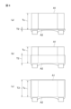
- FIG. 1 is a schematic perspective view of a multilayer ceramic capacitor 1.
- FIG. 2 is a cross-sectional view of the multilayer ceramic capacitor 1 taken along line II-II in FIG. 2 is a cross-sectional view of the multilayer ceramic capacitor 1 taken along line III-III in FIG.
- FIG. 3 is an enlarged view of a spacer 4 portion in the cross-sectional view of the multilayer ceramic capacitor 1 in FIG. 2 .
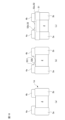
- 5A, 5B, and 5C are diagrams for explaining the covering state of a spacer-side covering portion 52 in a reinforcing material 5, in which (a), (b), and (c) are diagrams of an embodiment, and (d) and (e) are diagrams of a comparative example.
- FIG. 1A is a diagram illustrating a state in which a capacitor body 1A is covered by a capacitor side covering portion 51 of a reinforcing material 5.
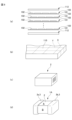
- FIG. 2 is a flowchart illustrating a method for manufacturing the multilayer ceramic capacitor 1.
- 3A to 3C are diagrams illustrating a laminate manufacturing step S1 and an external electrode forming step S2.
- 11A to 11C are diagrams illustrating a spacer arranging step S3.
- FIG. 11 is a diagram illustrating a reinforcing material placement step S4.
- 1 is a table showing the results of evaluation 1 and evaluation 2 performed on a multilayer ceramic capacitor 1 including a reinforcing material 5 according to an embodiment.
- a multilayer ceramic capacitor 1 will be described as an embodiment of a multilayer ceramic electronic component of the present invention, but the present invention is not limited thereto.
- the drawings may be drawn in a schematic and simplified manner in order to explain the contents of the invention, and the dimensional ratios of the depicted components or between the components may not match those dimensional ratios described in the specification.
- components described in the specification may be omitted in the drawings, or may be drawn with the number of components omitted.
- FIG. 1 is a schematic perspective view of a multilayer ceramic capacitor 1 according to an embodiment.
- FIG. 2 is a cross-sectional view of the multilayer ceramic capacitor 1 according to an embodiment taken along line II-II in FIG. 1.
- FIG. 3 is a cross-sectional view of the multilayer ceramic capacitor 1 according to an embodiment taken along line III-III in FIG. 1.
- the multilayer ceramic capacitor 1 is substantially rectangular and includes a capacitor body 1A having a laminate 2 and a pair of external electrodes 3 provided at both ends of the laminate 2, a spacer 4 attached to the capacitor body 1A, and a reinforcing material 5 covering the spacer 4 and a part of the capacitor body 1A.
- the laminate 2 also includes an inner layer 11 in which a dielectric layer 14 and an internal electrode layer 15 are laminated.
- the terms used to indicate the orientation of the multilayer ceramic capacitor 1 are the length direction L, which is the direction in which the pair of external electrodes 3 are provided in the multilayer ceramic capacitor 1.
- the direction in which the dielectric layers 14 and the internal electrode layers 15 are stacked is the stacking direction T.
- the direction that intersects both the length direction L and the stacking direction T is the width direction W. Note that in this embodiment, the width direction W is perpendicular to both the length direction L and the stacking direction T.
- Outer surface of laminate 2 Among the six outer surfaces of the laminate 2, a pair of outer surfaces facing each other in the stacking direction T is referred to as a first main surface A1 and a second main surface A2, a pair of outer surfaces facing each other in the width direction W is referred to as a first side surface B1 and a second side surface B2, and a pair of outer surfaces facing each other in the length direction L is referred to as a first end surface C1 and a second end surface C2.
- first main surface A1 and the second main surface A2 When it is not necessary to particularly distinguish between the first main surface A1 and the second main surface A2, they will be collectively referred to as a main surface A, when it is not necessary to particularly distinguish between the first side surface B1 and the second side surface B2, they will be collectively referred to as a side surface B, and when it is not necessary to particularly distinguish between the first end surface C1 and the second end surface C2, they will be collectively referred to as an end surface C.
- the laminate 2 preferably has rounded ridges R1, including the corners.
- the ridges R1 are the intersections of two surfaces of the laminate 2, i.e., the main surface A and the side surface B, the main surface A and the end surface C, or the side surface B and the end surface C.
- the laminate 2 comprises an inner layer portion 11 that forms a capacitance, an outer layer portion 12 that is arranged to sandwich the inner layer portion 11 in the stacking direction T, and a side gap portion 16 that is arranged to sandwich the inner layer portion 11 and the outer layer portion 12 in the width direction W.
- the inner layer portion 11 includes dielectric layers 14 and internal electrode layers 15 that are alternately stacked along a stacking direction T.
- the dielectric layer 14 is made of a ceramic material, such as a dielectric ceramic containing BaTiO3 as a main component.
- the internal electrode layer 15 includes a plurality of first internal electrode layers 15a and a plurality of second internal electrode layers 15b.
- the first internal electrode layers 15a and the second internal electrode layers 15b are alternately arranged.
- the first internal electrode layer 15a includes a first opposing portion 152a facing the second internal electrode layer 15b, and a first lead portion 151a drawn from the first opposing portion 152a to the first end face C1 side. An end of the first lead portion 151a is exposed to the first end face C1 and is electrically connected to the first external electrode 3a described later.
- the second internal electrode layer 15b includes a second opposing portion 152b facing the first internal electrode layer 15a, and a second lead portion 151b drawn from the second opposing portion 152b to the second end face C2. An end of the second lead portion 151b is electrically connected to the second external electrode 3b described later. Charges are stored in the first opposing portions 152a of the first internal electrode layers 15a and the second opposing portions 152b of the second internal electrode layers 15b.
- the internal electrode layer 15 is preferably formed from a metal material such as nickel (Ni), copper (Cu), silver (Ag), palladium (Pd), a silver-palladium (Ag-Pd) alloy, or gold (Au).
- a metal material such as nickel (Ni), copper (Cu), silver (Ag), palladium (Pd), a silver-palladium (Ag-Pd) alloy, or gold (Au).
- the outer layer portion 12 can be formed of the same material as the dielectric layer 14 of the inner layer portion 11 .
- the multilayer ceramic capacitor 1 includes a first side gap portion 16a that is disposed so as to sandwich the inner layer portion 11 and the outer layer portion 12 in the width direction W and that forms a first side surface B1 of the multilayer ceramic capacitor 1, and a second side gap portion 16b that forms a second side surface B2 of the multilayer ceramic capacitor 1.
- the side gap portion 16 can be formed of the same material as the dielectric layer 14.
- the external electrode 3 includes a first external electrode 3a provided on the first end face C1 and a second external electrode 3b provided on the second end face C2.
- the external electrode 3 covers not only the end face C but also a part of the main face A and the side face B continuing from the end face C.
- the end of the first extension portion 151a of the first internal electrode layer 15a is exposed to the first end face C1 and is electrically connected to the first external electrode 3a.
- the end of the second extension portion 151b of the second internal electrode layer 15b is exposed to the second end face C2 and is electrically connected to the second external electrode 3b.
- the external electrode 3 also includes, for example, a base electrode layer 30 and a plating layer 31. However, it is not necessarily required that the external electrode 3 has such a layered structure.
- the base electrode layer 30 is formed, for example, by applying and baking a conductive paste containing copper (Cu).
- the base electrode layer 30 may also contain glass or a ceramic material. However, the configuration of the base electrode layer 30 is not limited to this.
- the plating layer 31 includes a nickel (Ni) plating layer 31a disposed on the surface of the base electrode layer 30, and a tin (Sn) plating layer 31b disposed on the surface of the nickel (Ni) plating layer 31a. Note that the configuration of the plating layer 31 is not limited to this.
- the spacer 4 includes a pair of a first spacer 4a and a second spacer 4b.
- the first spacer 4a is disposed on one end face C1 side in the length direction L on the second main surface A2 side, which is the substrate mounting surface of the capacitor body 1A, and the second spacer 4b is disposed on the other end face C2 side.
- the spacers 4 are disposed so as to connect with the portion of the external electrode 3 disposed on the second main surface A2.
- the first spacer 4a is disposed on one end face C1 side in the length direction L on the first side surface B1 side, which is the substrate mounting surface of the capacitor body 1A, and the second spacer 4b is disposed on the other end face C2 side.
- spacer main surfaces SA the two surfaces that face the stacking direction T are referred to as spacer main surfaces SA
- spacer end surfaces SC the two surfaces that face the length direction L are referred to as spacer end surfaces SC
- spacer side surfaces SB the two surfaces that face the width direction W are referred to as spacer side surfaces SB.
- the spacer end face SC closer to the center of the length direction L of the capacitor body 1A will be described as the central spacer end face SC1
- the spacer end face SC on the outside of the length direction L of the laminate 2 will be described as the outer spacer end face SC2.
- the spacer main surface SA on the capacitor body 1A side will be described as the body-side spacer main surface SA1
- the spacer main surface SA on the other side will be described as the mounting-side spacer main surface SA2.
- the board mounting surface of the capacitor body 1A is the first side surface B1
- the spacer side surface SB on the capacitor body 1A side will be described as the body-side spacer side surface SB1
- the spacer side surface SB on the other side will be described as the mounting-side spacer side surface SB2.
- the length in the longitudinal direction L of each spacer 4 is longer than the external electrode 3 arranged on the second main surface A2. That is, the central spacer end face SC1 of each spacer 4 is arranged beyond the external electrode 3, and there is a portion where the body-side spacer main surface SA1 of the spacer 4 is in direct contact with the second main surface A2 of the laminate 2. Furthermore, without being limited to this, the length in the longitudinal direction L of each spacer 4 may be shorter than the external electrode arranged on the second main surface A2. The same is true when the substrate mounting surface of the capacitor body 1A is the first side surface B1.
- the external electrode 3 is composed of the base electrode layer 30 and the plating layer 31 covering it, and the spacer 4 is disposed on the surface of the plating layer 31.
- the spacer 4 may be disposed on the surface of the base electrode layer 30, and a second plating layer may be disposed to cover the spacer 4 and the base electrode layer 30. By disposing the second plating layer, the adhesive strength between the spacer 4 and the base electrode layer 30 is improved.
- the spacer 4 contains either copper (Cu) or nickel (Ni) and tin (Sn) as metal powder.
- the copper (Cu) and nickel (Ni) may be coated with silver (Ag).
- the spacer 4 may further contain silver (Ag) as a metal constituting an intermetallic compound.
- Intermetallic compounds formed by adding tin (Sn) to either copper (Cu) or nickel (Ni) have a melting point that does not melt even when soldering is performed when mounting the multilayer ceramic capacitor 1 on a wiring board, and do not deform due to heat. Therefore, the shape of the spacer 4 can be reliably maintained, and it is possible to arrange it while maintaining the desired shape even during soldering.
- intermetallic compounds formed by adding tin (Sn) to an alloy of copper (Cu) and nickel (Ni) are preferable as components for forming the spacer 4.
- Phenol resin may be included in the metal region MP formed by the metal powder.
- the phenol resin coats the particles of the intermetallic compound and is scattered so as to fill the gaps between the particles.
- the phenol resin may not completely coat the particles of the intermetallic compound.
- the amount of gas generated during the heat treatment for forming the spacer 4 can be reduced, thereby reducing voids within the spacer 4.
- the phenol resin may be exposed on the surface of the spacer 4 and coat at least a portion of the surface of the spacer 4. By coating the surface of the spacer 4 with the phenol resin, the smoothness of the surface of the spacer 4 is improved, and the mechanical strength of the spacer 4 can be increased.
- phenolic resins include novolac-type phenolic resins such as phenol novolac resin, phenol aralkyl resin, cresol novolac resin, Tcrt-butylphenol novolac resin, and nonylphenol novolac resin, resol-type phenolic resin, and polyoxystyrene such as polyparaoxystyrene.
- the area ratio of the phenolic resin in the spacer 4 is preferably 1% to 20% in the LT cross section perpendicular to the width direction W of the spacer 4, and more preferably 5% to 15%. If it is less than 1%, the effect of the phenolic resin cannot be fully exerted, and if it exceeds 20%, the adhesive strength of the spacer to the external electrode may decrease.
- the percentage (%) of the area occupied by the phenolic resin in the spacer 4 can be calculated, for example, by polishing the spacer 4 in the width direction W up to the center of the width direction W, enlarging the polished surface with a microscope (BX-51) at a total magnification of 50 times, and photographing it with a digital camera for microscopes (Olympus DP22).
- the photographed image obtained is binarized to separate it into metal regions MP and resin regions RP, and the percentage (%) of the area occupied by the phenolic resin can be calculated from the areas of the metal regions MP, metal powder MF, resin regions RP, and voids P using the formula: (area of resin regions RP) / (area of metal regions MP + area of metal powder MF + area of resin regions RP + area of voids P) x 100.
- FIG. 4 is an enlarged view of the spacer 4 in the cross-sectional view of the multilayer ceramic capacitor 1 in FIG. 2.
- metal powder MF may be included in the resin region RP formed by the phenolic resin. The metal powder MF can inhibit the shrinkage of the phenolic resin, thereby mitigating the shrinkage stress caused by the phenolic resin.
- the spacer 4 preferably has a porosity of 20% or less in the region Z up to 5 ⁇ m from the interface with the external electrode 3. By keeping the porosity low, the bonding area of the spacer 4 that is bonded to the external electrode 3 increases, improving the bonding strength with the external electrode 3.
- a void P is formed inside the spacer 4, and the maximum diameter of the void P is preferably 1/2 or less of the maximum dimension of the thickness of the spacer 4 in the stacking direction T. If it is greater than 1/2, cracks are more likely to occur starting from the void P, reducing the strength of the spacer 4.
- the maximum diameter of the void P formed inside the spacer 4 is preferably 1/2 or less of the maximum dimension of the thickness of the spacer 4 in the width direction W.
- the present invention is not limited to this and may contain other metal components, or may contain a resin other than the phenolic resin, such as an epoxy resin or rosin, or a glass component.
- the spacer may also be formed without containing a resin.
- the terminal may be manufactured from a material containing copper, such as copper or a copper alloy, and may be arranged to be connected via Ni plating and solder.
- the direction discrimination means indicates the direction for facing the second main surface A2 or the first side surface B1 on which the spacer 4 is arranged to the wiring board when mounting the multilayer ceramic capacitor 1 on the wiring board, and can be a means for coloring the spacer 4 in a color different from the external electrode 3, a means for printing a direction identification mark for identifying the direction such as a QR code (registered trademark), or a means for providing a recess in a part of the laminate.
- the phenolic resin contained in the spacer 4 may be exposed on the surface of the spacer 4 so that it has a color different from that of the external electrode 3.
- the direction discrimination mark is not limited to the spacer 4, and may be provided on the laminate 2. Even if the spacer 4 is larger than the external electrode 3, a direction discrimination means may be provided.
- the spacer 4 and the external electrode 3 have the same color, it is difficult to tell which side the spacer 4 is attached to when viewed from above, which can lead to errors in image processing.
- providing a direction identification mark can prevent such errors in image processing.
- the reinforcing material 5 includes a capacitor side covering portion 51 that covers a predetermined length in the stacking direction T of the capacitor body 1A, and a spacer side covering portion 52 that is continuous with the capacitor side covering portion 51 and is arranged on the spacer 4 side.
- the reinforcing material 5 includes the capacitor side covering portion 51 that covers a predetermined length in the width direction W of the capacitor body 1A, and the spacer side covering portion 52 that is continuous with the capacitor side covering portion 51 and is arranged on the spacer 4 side.
- the reinforcing material 5 includes an insulating resin, and in the embodiment, the reinforcing material 5 is mainly made of an insulating resin.
- the surface of the insulating resin may be coated with an insulating water repellent agent.
- the insulating resin may contain ceramics, glass, etc.
- the reinforcing material 5 has a higher adhesion strength with the laminate 2 than an intermetallic compound.
- the reinforcing material 5 is mainly composed of an epoxy resin, and a phenolic resin can be combined with this as a hardener.
- a phenolic resin can be combined with this as a hardener.
- hardeners such as acid anhydride-based, amine-based, and ester-based hardeners can be used.
- a hardening accelerator may be further added to the epoxy resin. It may be formed only from a water repellent agent.
- the spacer side covering portion 52 includes side portions 52a covering the two spacer side surfaces SB of each of the two spacers 4, and a central portion 52b that is disposed between a central spacer end face SC1 of one spacer 4 and a central spacer end face SC1 of the other spacer 4 and covers the second main surface A2 side of the capacitor body 1A (laminate 2).
- the central portion 52b covers the central spacer end faces SC1 of each of the two spacers 4.
- the central portion 52b connects the central spacer end face SC1 of one spacer 4 to the central spacer end face SC1 of the other spacer 4.
- the central portion 52b does not necessarily need to be continuous between the first spacer 4a and the second spacer 4b.
- the central portion 52b may be divided into, for example, one that covers the central spacer end face SC1 of the first spacer 4a and a part of the second main surface A2 side of the capacitor body 1A (laminate 2), and one that covers the central spacer end face SC1 of the second spacer 4b and a part of the second main surface A2 side of the capacitor body 1A (laminate 2), and arranged discontinuously.
- the spacer side covering portion 52 also covers the outer spacer end face SC2, but is not limited to this and does not have to cover the outer spacer end face SC2.
- FIG. 5 is a diagram for explaining the covering state of the spacer side covering portion 52 in the reinforcing material 5, with FIGS. 5(a), (b), and (c) showing an embodiment and FIGS. 5(d) and (e) showing a comparative embodiment.
- the stacking direction length T1 of the side portion 52a is 4.9% or more of the stacking direction length Ts of the spacer 4.
- the side portion 52a does not cover the mounting side spacer main surface SA2 of the spacer main surface SA of the spacer 4, and is therefore less than 100%. In other words, 0.049 ⁇ T1/Ts ⁇ 1.
- Figure 5(a) shows the case where T1/Ts is approximately 0.5
- Figure 5(b) shows the case where T1/Ts is approximately 0.95.
- Figure 5(c) shows a case where the mounting side spacer main surface SA2 is inclined relative to the body side spacer main surface SA1.
- T1/Ts is approximately 0.7 at the portion of the mounting side spacer main surface SA2 furthest from the body side spacer main surface SA1, but T1/Ts is approximately 1 at the portion of the mounting side spacer main surface SA2 closest to the body side spacer main surface SA1.
- the reinforcing material 5 does not extend to the mounting side spacer main surface SA2, and no reinforcing material 5 is disposed on the mounting side spacer main surface SA2.
- Figure 5(d) shows a comparative example where T1/Ts is greater than 1 and reinforcing material 5 is also placed on the mounting side spacer main surface SA2.
- Figure 5(e) shows a comparative example in which the mounting side spacer main surface SA2 is inclined relative to the body side spacer main surface SA1.
- T1/Ts is approximately 0.9 in the portion where the mounting side spacer main surface SA2 is furthest from the body side spacer main surface SA1, but T1/Ts is 1 or more in the portion where the mounting side spacer main surface SA2 is closest to the body side spacer main surface SA1.
- reinforcing material 5 is present on the mounting side spacer main surface SA2.
- the reinforcing material 5 extends to the mounting-side spacer main surface SA2, so when the multilayer ceramic capacitor 1 is mounted on a substrate, the presence of the reinforcing material 5 inhibits electrical continuity between the spacer 4 and the substrate. Furthermore, if the reinforcing material 5 covers the mounting-side spacer main surface SA2 of the spacer 4, the solder will not adhere to the spacer 4 during mounting, which may increase mounting defects.
- the reinforcing material 5 is not disposed between the external electrode 3 and the spacer 4 on the main body side spacer main surface SA1 of the spacer 4. Since the reinforcing material 5 is not disposed between the external electrode 3 and the spacer 4, electrical connection between the external electrode 3 and the spacer 4 can be ensured.
- the reinforcing material 5 may be arranged so as to fill the gap. If the reinforcing material 5 fills the gap, the bonding area between the reinforcing material 5 and the spacer 4 increases, and the bonding strength increases. Note that if the gap is not completely filled with the reinforcing material 5, the gap can mitigate the propagation of vibration.
- the reinforcing material 5 cover a larger area of surfaces other than the spacer main surface SA, as this improves the reinforcing effect.
- FIG. 6 is a diagram illustrating the state in which capacitor body 1A is covered by capacitor side covering part 51 of reinforcing material 5.
- Capacitor side covering part 51 covers a predetermined length range in the stacking direction on the second main surface A2 side of capacitor body 1A. If the length in the stacking direction of capacitor body 1A is Tc and the length in the stacking direction of capacitor side covering part 51 is T2, T2/Tc is about 0.05 in Fig. 6(a), about 0.5 in Fig. 6(b), and about 1.1 in Fig. 6(c).
- the covering area may be partial as in Figures 6(a) and 6(a), but it is preferable for it to cover the entire capacitor body 1A as in Figure 6(c).
- the reinforcing material 5 it is preferable for the reinforcing material 5 to cover a portion of the spacer 4 and the entire capacitor body 1A.
- the measurement of the length of the reinforcing material 5 in the stacking direction T described above can be carried out, for example, as follows.
- the multilayer ceramic capacitor 1 joined to the wiring board by solder is polished in the width direction W to the LT cross section position where the multilayer ceramic capacitor 1 and the reinforcing material 5 can be seen.
- a microscope e.g., BX-51, manufactured by Olympus
- a digital camera for a microscope (e.g., DP22, manufactured by Olympus)
- the length of the reinforcing material 5 in the stacking direction T is measured by appropriately adjusting the total magnification to 10 to 50 times, etc.
- the reinforcing material 5 includes a spacer-side covering portion 52 that covers 4.9% or more of each of the two spacers in the stacking direction T, and a capacitor-side covering portion 51 that is continuous with the spacer-side covering portion 52 and covers the spacer side of the outer periphery of the capacitor body 1A. This makes it possible to ensure resistance to substrate bending while maintaining the effect of suppressing acoustic noise.
- the spacer side covering portion 52 of the reinforcing material 5 continuously covers the central spacer end face SC1 of the two spacer end faces SC and the two spacer side faces SB. This increases the area of the spacer 4 covered by the reinforcing material 5, thereby making it possible to further strengthen the resistance to bending of the board.
- the reinforcing material 5 covers the entire capacitor body 1A, it can further strengthen the bending resistance of the board.
- (Method of Manufacturing Multilayer Ceramic Capacitor 1) 7 is a flowchart illustrating a method for manufacturing the multilayer ceramic capacitor 1.
- the method for manufacturing the multilayer ceramic capacitor 1 includes a laminate manufacturing step S1, an external electrode forming step S2, a spacer arranging step S3, and a reinforcing material arranging step S4.
- FIG. 8 is a diagram illustrating the laminate manufacturing step S1 and the external electrode forming step S2.
- FIG. 9 is a diagram illustrating the spacer arrangement step S3.
- FIG. 10 is a diagram illustrating the reinforcing material arrangement step S4.
- a ceramic slurry containing ceramic powder, a binder, and a solvent is formed into a sheet shape on the surface of a carrier film using a die coater, a gravure coater, a microgravure coater, or the like to prepare a laminated ceramic green sheet 101 that will become the dielectric layer 14.
- a conductive paste is printed in stripes on the laminated ceramic green sheet 101 by screen printing, inkjet printing, gravure printing, or the like, and a conductive pattern 102 that will become the internal electrode layer 15 is printed on the surface of the laminated ceramic green sheet 101 to prepare a material sheet 103.
- multiple material sheets 103 are stacked so that the conductive patterns 102 face the same direction and are offset, for example, by half a pitch in the length direction L between adjacent material sheets 103. Furthermore, outer layer ceramic green sheets 112 that will become the outer layer 12 are stacked on both sides of the multiple stacked material sheets 103.
- the stacked material sheets 103 and the outer layer ceramic green sheets 112 are pressed together using a hydrostatic press or the like to create the mother block 110 shown in Figure 8(b).
- the mother block 110 is cut along the cutting line X shown in FIG. 8(b) and along the cutting line Y that intersects with the cutting line X to produce a plurality of laminates 2 shown in FIG. 8(c).
- Example electrode formation step S2 Next, a conductive paste containing copper (Cu) is applied to the end faces C of the laminate 2 and baked to form the base electrode layer 30.
- the base electrode layer 30 is formed not only on the end faces C on both sides of the laminate 2 but also on the other end faces C on both sides of the laminate 2. , extending to the main surface A and side surface B of the laminate 2 and covering a portion of the end surface C of the main surface A.
- a nickel (Ni) plating layer 31a and a tin (Sn) plating layer 31b disposed on the surface of the nickel (Ni) plating layer 31a are formed as plating layers 31 on the surface of the base electrode layer 30, and the resulting structure shown in FIG.
- a capacitor body 1A shown in (d) is manufactured.
- Spacer placement step S3 A spacer manufacturing paste 41 used for manufacturing the spacers is prepared.
- the spacer manufacturing paste 41 contains metals made of copper (Cu), nickel (NI), tin (Sn), and silver (Ag), a phenol resin, a solvent, and an additive.
- rosin may be contained instead of the phenol resin.
- phenolic resins include novolac-type phenolic resins such as phenol novolac resin, phenol aralkyl resin, cresol novolac resin, tcrt-butylphenol novolac resin, and nonylphenol novolac resin, resol-type phenolic resin, and polyoxystyrenes such as polyparaoxystyrene.
- FIG. 9 is a diagram illustrating the spacer arrangement step S3. As shown in FIG. 9A, first, a spacer manufacturing paste 41 is placed on a holding substrate 40 by a screen printing method, a dispense method, or the like.
- the capacitor body 1A is mounted on the upper surface of the holding substrate 40 with the second main surface A2 facing the holding substrate 40. At this time, the external electrode 3 of the capacitor body 1A and the spacer manufacturing paste 41 are aligned, and the spacer manufacturing paste 41 adheres to the capacitor body 1A.
- the heating process is carried out.
- the metal in the paste produces an intermetallic compound and the metal region MP is formed
- some of the phenolic resin is taken into the metal region MP and some is expelled from the metal region MP, while hardening, forming a spacer 4 bonded to the capacitor body 1A.
- an example of the spacer material is shown to include an intermetallic compound and phenolic resin, but the material is not limited to this and may include other types of metal components, or may include resins such as epoxy resins or rosin, or glass components, in addition to phenolic resin. It may also be formed without including resin.
- the capacitor body 1A is separated from the holding substrate 40 together with the spacer 4.
- the spacer may be formed by placing a spacer manufacturing paste in a desired shape directly on the surface of the capacitor body 1A and performing a heat treatment.
- FIG. 10A and 10B are diagrams illustrating the reinforcing material arrangement step S4.
- the surface of the capacitor body 1A on which the spacer 4 is arranged is cleaned with a solvent.
- FIG. 10A after the cleaning is completed, The capacitor body 1A with the spacers 4 disposed thereon is aligned so that the spacers 4 face upward.
- a dispenser or squeegee printing is used to form an insulating resin layer that will become the central portion 52b of the reinforcing material 5 between the first spacer 4a and the second spacer 4b on the capacitor body 1A on which the spacer 4 is arranged.
- the amount of insulating resin that is wetted onto the central spacer end surface SC1 can be changed by changing the amount of insulating resin.
- insulating resin When insulating resin is to be inserted into the interface between the spacer 4 and the laminate 2, it can be inserted by drawing a vacuum after placing the insulating resin.
- the amount of insertion can be controlled by changing the vacuuming time and pressure.
- an insulating resin is applied so as to extend over the outer periphery of the capacitor body 1 A and the outer periphery of the spacer 4 .
- the applied insulating resin is then heated at 100 to 200° C. for 20 to 80 minutes, whereby the insulating resin hardens to form a capacitor side covering portion 51 on the outer periphery of the capacitor body 1A and a spacer side covering portion 52 on the outer periphery of the spacer 4.
- the multilayer ceramic capacitor 1 is manufactured.
- the capacitor body 1A used was as follows. Length direction L: 1.6 mm Width direction W: 0.8mm Stacking direction T: 0.8 mm Main component of internal electrode: Ni Dielectric layer: BaTiO3 Main component of the base electrode layer: Cu First plating layer: Ni Second plating layer: Sn
- the components of the spacer 4 are as follows: The mixture was 31.5 wt% Cu-10 wt% Ni powder with a D50 (median diameter) of 5 ⁇ m, 58.5 wt% solder powder with a composition of Sn-3 wt%, Ag-0.5 wt%, and Cu with a D50 of 5 ⁇ m, and a total of 10 wt% rosin, solvent, and additives.
- the reinforcing material 5 is an insulating resin that is mainly made of epoxy resin and has phenolic resin as a hardener.
- the multilayer ceramic capacitor 1 was mounted on a JIS board with a thickness of 1.6 mm using lead-free solder and was held at a bend of 4 mm for 5 seconds.
- the width direction W was cut down to 1/2.
- the multilayer ceramic capacitor near the mounting surface was observed using a microscope (BX-51, Olympus) connected to a digital camera for microscopes (DP22, Olympus) with the total magnification appropriately adjusted to 10x.
- a sound-collecting microphone was placed opposite the mounting board portion on which the multilayer ceramic capacitor 1 was placed.
- An alternating current having a frequency of 3 kHz and a voltage of 1 Vpp was applied to the multilayer ceramic capacitor 1, and the resonance level of the multilayer ceramic capacitor 1 was measured by a sound collecting microphone.
- the resonance of the multilayer ceramic capacitor 1 was collected by the sound collecting microphone, and the output of the sound collecting microphone was input to an FFT (Fast Fourier Transform) analyzer via a sound collecting meter, where the sound pressure level was analyzed.
- FFT Fast Fourier Transform
- FIG. 11 is a table showing the results of evaluations 1 and 2 performed on the multilayer ceramic capacitor 1 including the reinforcing material 5 according to the embodiment.
- Evaluation 1 in the embodiments in which the length of the spacer side covering portion 52 relative to the spacer length in the stacking direction T was 4.9% and 13.5%, the crack occurrence rate was less than 50%, while in the comparative embodiments in which the length was 0%, 1.2%, and 3.6%, the crack occurrence rate was 50% or more.
- the provision of the reinforcing material 5 had an effect of improving the sound pressure level.
- the length of the spacer side covering portion relative to the spacer length in the stacking direction improved by 10% or more when the length was 1.2% or more, including 4.9% or more in the embodiment.
- the multilayer ceramic capacitor 1 of the embodiment reduces the rate of crack occurrence and also reduces the occurrence of squealing noise.
- the spacer material was shown to include an intermetallic compound and rosin, but the material is not limited to this and may include other types of metal components, or may include resins such as epoxy resins or phenolic resins or glass components other than rosin. It may also be formed without including resin.
- the above describes an embodiment of the present invention, but the present invention is not limited to the embodiment, and can be implemented in various forms without departing from the gist of the present invention.
- the present invention includes the following combinations.
- a capacitor body including a laminate in which dielectric layers and internal electrode layers are alternately laminated, the laminate having two main surfaces facing each other in a lamination direction, two end faces facing each other in a length direction intersecting the lamination direction, and two side surfaces facing each other in a width direction intersecting the lamination direction and the length direction, and two external electrodes disposed on each of the two end faces, connected to the internal electrode layers, and extending to the two main faces to cover a portion of the main faces; and a capacitor body including two external electrodes disposed on one end face side and the other end face side on one main face side of the capacitor body, with the external electrode covering the portion of the main faces sandwiched therebetween, the external electrode being disposed on one end face side and the other end face side, each of which is disposed in the lamination direction.
- a multilayer ceramic electronic component comprising two spacers having two spacer main surfaces facing each other in the stacking direction, two spacer end faces facing each other in the length direction, and two spacer side surfaces facing each other in the width direction; a spacer side covering portion covering 5.0% or more of each of the two spacers in the stacking direction; and a capacitor side covering portion continuing from the spacer side covering portion and covering the spacer side of the outer periphery of the capacitor body, the spacer side covering portion being a reinforcing material that continuously covers the opposing spacer end faces of the two spacers that face each other and the two spacer side faces.
- each of the spacers has two spacer main surfaces facing each other in the stacking direction, two spacer end faces facing each other in the length direction, and two spacer side faces facing each other in the width direction, and in each of the spacers, the spacer side covering portion of the reinforcing material covers the outer spacer end face that is on the outer side in the length direction of the laminate, out of the two spacer end faces.
- ⁇ 4> A multilayer ceramic electronic component according to any one of ⁇ 1> to ⁇ 3>, in which an orientation identification mark is arranged on the laminate.
- ⁇ 5> A multilayer ceramic electronic component according to any one of ⁇ 1> to ⁇ 4>, in which a direction identification mark is arranged on the spacer.
- SA Spacer main surface SA1: Body-side spacer main surface SA2: Mounting-side spacer main surface SB: Spacer side surface SC: Spacer end surface SC1: Center-side spacer end surface SC2: Outer spacer end surface 1: Multilayer ceramic capacitor 1A: Capacitor body 2: Multilayer body 3: External electrode 3a: First external electrode 3b: Second external electrode 4: Spacer 4a: First spacer 4b: Second spacer 5: Reinforcing material 51: Capacitor-side covering portion 52: Spacer-side covering portion 52a: Side portion 52b: Center portion
Landscapes
- Engineering & Computer Science (AREA)
- Power Engineering (AREA)
- Microelectronics & Electronic Packaging (AREA)
- Manufacturing & Machinery (AREA)
- Ceramic Engineering (AREA)
- Chemical & Material Sciences (AREA)
- Physics & Mathematics (AREA)
- Electromagnetism (AREA)
- Inorganic Chemistry (AREA)
- Ceramic Capacitors (AREA)
- Fixed Capacitors And Capacitor Manufacturing Machines (AREA)
Priority Applications (3)
| Application Number | Priority Date | Filing Date | Title |
|---|---|---|---|
| CN202480022019.8A CN120883301A (zh) | 2023-03-30 | 2024-01-16 | 层叠陶瓷电子部件 |
| JP2025509779A JPWO2024202403A1 (https=) | 2023-03-30 | 2024-01-16 | |
| US19/338,092 US20260018340A1 (en) | 2023-03-30 | 2025-09-24 | Multilayer ceramic electronic component |
Applications Claiming Priority (2)
| Application Number | Priority Date | Filing Date | Title |
|---|---|---|---|
| JP2023-055772 | 2023-03-30 | ||
| JP2023055772 | 2023-03-30 |
Related Child Applications (1)
| Application Number | Title | Priority Date | Filing Date |
|---|---|---|---|
| US19/338,092 Continuation US20260018340A1 (en) | 2023-03-30 | 2025-09-24 | Multilayer ceramic electronic component |
Publications (1)
| Publication Number | Publication Date |
|---|---|
| WO2024202403A1 true WO2024202403A1 (ja) | 2024-10-03 |
Family
ID=92904904
Family Applications (1)
| Application Number | Title | Priority Date | Filing Date |
|---|---|---|---|
| PCT/JP2024/000954 Ceased WO2024202403A1 (ja) | 2023-03-30 | 2024-01-16 | 積層セラミック電子部品 |
Country Status (4)
| Country | Link |
|---|---|
| US (1) | US20260018340A1 (https=) |
| JP (1) | JPWO2024202403A1 (https=) |
| CN (1) | CN120883301A (https=) |
| WO (1) | WO2024202403A1 (https=) |
Citations (6)
| Publication number | Priority date | Publication date | Assignee | Title |
|---|---|---|---|---|
| JPS58101417A (ja) * | 1981-12-11 | 1983-06-16 | 日本電気株式会社 | チップ型有極電子部品 |
| JP2016111280A (ja) * | 2014-12-10 | 2016-06-20 | 東光株式会社 | 電子部品及びその製造方法 |
| WO2016121575A1 (ja) * | 2015-01-30 | 2016-08-04 | 株式会社村田製作所 | 電子部品の製造方法および電子部品 |
| WO2018101405A1 (ja) * | 2016-12-01 | 2018-06-07 | 株式会社村田製作所 | チップ型電子部品 |
| JP2018190952A (ja) * | 2017-05-04 | 2018-11-29 | サムソン エレクトロ−メカニックス カンパニーリミテッド. | 積層型電子部品及びその実装基板 |
| JP2022099069A (ja) * | 2020-12-22 | 2022-07-04 | 株式会社村田製作所 | 積層セラミックコンデンサ及び積層セラミックコンデンサの製造方法 |
-
2024
- 2024-01-16 CN CN202480022019.8A patent/CN120883301A/zh active Pending
- 2024-01-16 JP JP2025509779A patent/JPWO2024202403A1/ja active Pending
- 2024-01-16 WO PCT/JP2024/000954 patent/WO2024202403A1/ja not_active Ceased
-
2025
- 2025-09-24 US US19/338,092 patent/US20260018340A1/en active Pending
Patent Citations (6)
| Publication number | Priority date | Publication date | Assignee | Title |
|---|---|---|---|---|
| JPS58101417A (ja) * | 1981-12-11 | 1983-06-16 | 日本電気株式会社 | チップ型有極電子部品 |
| JP2016111280A (ja) * | 2014-12-10 | 2016-06-20 | 東光株式会社 | 電子部品及びその製造方法 |
| WO2016121575A1 (ja) * | 2015-01-30 | 2016-08-04 | 株式会社村田製作所 | 電子部品の製造方法および電子部品 |
| WO2018101405A1 (ja) * | 2016-12-01 | 2018-06-07 | 株式会社村田製作所 | チップ型電子部品 |
| JP2018190952A (ja) * | 2017-05-04 | 2018-11-29 | サムソン エレクトロ−メカニックス カンパニーリミテッド. | 積層型電子部品及びその実装基板 |
| JP2022099069A (ja) * | 2020-12-22 | 2022-07-04 | 株式会社村田製作所 | 積層セラミックコンデンサ及び積層セラミックコンデンサの製造方法 |
Also Published As
| Publication number | Publication date |
|---|---|
| CN120883301A (zh) | 2025-10-31 |
| JPWO2024202403A1 (https=) | 2024-10-03 |
| US20260018340A1 (en) | 2026-01-15 |
Similar Documents
| Publication | Publication Date | Title |
|---|---|---|
| CN103915252B (zh) | 嵌入式多层陶瓷电子元件以及具有嵌入式多层陶瓷电子元件的印刷电路板 | |
| JP7136427B2 (ja) | 積層セラミック電子部品及びその実装基板 | |
| US8305729B2 (en) | Laminated ceramic electronic component | |
| JP5855593B2 (ja) | 基板内蔵用積層セラミック電子部品及びその製造方法、基板内蔵用積層セラミック電子部品を備える印刷回路基板 | |
| JP2018098475A (ja) | 積層セラミックコンデンサ | |
| JP2017069417A (ja) | 積層コンデンサ | |
| JP2015076600A (ja) | 基板内蔵用積層セラミック電子部品及び積層セラミック電子部品内蔵型印刷回路基板 | |
| JP2011228334A (ja) | セラミック電子部品 | |
| US20260024699A1 (en) | Multilayer ceramic electronic component | |
| JP7647920B2 (ja) | 積層セラミックコンデンサ及びバンプ製造用ペースト | |
| JP7690995B2 (ja) | 積層セラミックコンデンサ及びバンプ製造用ペースト | |
| US20260018340A1 (en) | Multilayer ceramic electronic component | |
| JP2023056513A (ja) | 積層型電子部品 | |
| US20260011503A1 (en) | Multilayer ceramic electronic component | |
| US20260011502A1 (en) | Laminated ceramic electronic component | |
| WO2023085264A1 (ja) | 積層セラミックコンデンサ及びバンプ製造用ペースト | |
| US20260018337A1 (en) | Multilayer ceramic electronic component | |
| US20260011504A1 (en) | Multilayer ceramic electronic component | |
| US20260058062A1 (en) | Multilayer ceramic electronic component | |
| WO2025163971A1 (ja) | 積層セラミック電子部品 | |
| WO2025163972A1 (ja) | 積層セラミック電子部品 | |
| WO2025163973A1 (ja) | 積層セラミック電子部品 | |
| WO2025046969A1 (ja) | 積層セラミック電子部品 | |
| JP2024022341A (ja) | 積層セラミックコンデンサおよび積層セラミックコンデンサの実装構造 | |
| WO2025046970A1 (ja) | 積層セラミック電子部品 |
Legal Events
| Date | Code | Title | Description |
|---|---|---|---|
| 121 | Ep: the epo has been informed by wipo that ep was designated in this application |
Ref document number: 24778549 Country of ref document: EP Kind code of ref document: A1 |
|
| ENP | Entry into the national phase |
Ref document number: 2025509779 Country of ref document: JP Kind code of ref document: A |
|
| WWE | Wipo information: entry into national phase |
Ref document number: 2025509779 Country of ref document: JP |
|
| WWE | Wipo information: entry into national phase |
Ref document number: 202480022019.8 Country of ref document: CN |
|
| NENP | Non-entry into the national phase |
Ref country code: DE |
|
| WWP | Wipo information: published in national office |
Ref document number: 202480022019.8 Country of ref document: CN |
|
| 122 | Ep: pct application non-entry in european phase |
Ref document number: 24778549 Country of ref document: EP Kind code of ref document: A1 |