WO2024201707A1 - 光学部品、透明封止部材、基板、及び光学部品の製造方法 - Google Patents
光学部品、透明封止部材、基板、及び光学部品の製造方法 Download PDFInfo
- Publication number
- WO2024201707A1 WO2024201707A1 PCT/JP2023/012494 JP2023012494W WO2024201707A1 WO 2024201707 A1 WO2024201707 A1 WO 2024201707A1 JP 2023012494 W JP2023012494 W JP 2023012494W WO 2024201707 A1 WO2024201707 A1 WO 2024201707A1
- Authority
- WO
- WIPO (PCT)
- Prior art keywords
- layer
- stress relaxation
- sealing member
- optical component
- transparent sealing
- Prior art date
- Legal status (The legal status is an assumption and is not a legal conclusion. Google has not performed a legal analysis and makes no representation as to the accuracy of the status listed.)
- Ceased
Links
Images



Classifications
-
- H—ELECTRICITY
- H10—SEMICONDUCTOR DEVICES; ELECTRIC SOLID-STATE DEVICES NOT OTHERWISE PROVIDED FOR
- H10W—GENERIC PACKAGES, INTERCONNECTIONS, CONNECTORS OR OTHER CONSTRUCTIONAL DETAILS OF DEVICES COVERED BY CLASS H10
- H10W76/00—Containers; Fillings or auxiliary members therefor; Seals
- H10W76/60—Seals
-
- H—ELECTRICITY
- H10—SEMICONDUCTOR DEVICES; ELECTRIC SOLID-STATE DEVICES NOT OTHERWISE PROVIDED FOR
- H10H—INORGANIC LIGHT-EMITTING SEMICONDUCTOR DEVICES HAVING POTENTIAL BARRIERS
- H10H20/00—Individual inorganic light-emitting semiconductor devices having potential barriers, e.g. light-emitting diodes [LED]
- H10H20/01—Manufacture or treatment
- H10H20/036—Manufacture or treatment of packages
-
- H—ELECTRICITY
- H10—SEMICONDUCTOR DEVICES; ELECTRIC SOLID-STATE DEVICES NOT OTHERWISE PROVIDED FOR
- H10F—INORGANIC SEMICONDUCTOR DEVICES SENSITIVE TO INFRARED RADIATION, LIGHT, ELECTROMAGNETIC RADIATION OF SHORTER WAVELENGTH OR CORPUSCULAR RADIATION
- H10F77/00—Constructional details of devices covered by this subclass
- H10F77/40—Optical elements or arrangements
- H10F77/407—Optical elements or arrangements indirectly associated with the devices
-
- H—ELECTRICITY
- H10—SEMICONDUCTOR DEVICES; ELECTRIC SOLID-STATE DEVICES NOT OTHERWISE PROVIDED FOR
- H10F—INORGANIC SEMICONDUCTOR DEVICES SENSITIVE TO INFRARED RADIATION, LIGHT, ELECTROMAGNETIC RADIATION OF SHORTER WAVELENGTH OR CORPUSCULAR RADIATION
- H10F77/00—Constructional details of devices covered by this subclass
- H10F77/50—Encapsulations or containers
-
- H—ELECTRICITY
- H10—SEMICONDUCTOR DEVICES; ELECTRIC SOLID-STATE DEVICES NOT OTHERWISE PROVIDED FOR
- H10H—INORGANIC LIGHT-EMITTING SEMICONDUCTOR DEVICES HAVING POTENTIAL BARRIERS
- H10H20/00—Individual inorganic light-emitting semiconductor devices having potential barriers, e.g. light-emitting diodes [LED]
- H10H20/01—Manufacture or treatment
- H10H20/036—Manufacture or treatment of packages
- H10H20/0363—Manufacture or treatment of packages of optical field-shaping means
-
- H—ELECTRICITY
- H10—SEMICONDUCTOR DEVICES; ELECTRIC SOLID-STATE DEVICES NOT OTHERWISE PROVIDED FOR
- H10H—INORGANIC LIGHT-EMITTING SEMICONDUCTOR DEVICES HAVING POTENTIAL BARRIERS
- H10H20/00—Individual inorganic light-emitting semiconductor devices having potential barriers, e.g. light-emitting diodes [LED]
- H10H20/80—Constructional details
- H10H20/85—Packages
- H10H20/855—Optical field-shaping means, e.g. lenses
Definitions
- the present invention relates to optical components, transparent sealing members, substrates, and methods for manufacturing optical components.
- Optical components such as light-emitting devices or optical sensors have a structure in which a transparent sealing member is bonded to a substrate carrying an optical element, and the optical element is sealed with the transparent sealing member.
- the optical element is a light-emitting element (e.g., an LED) or a light-receiving element (e.g., a photodiode).
- the transparent sealing member is glass, and is bonded to the substrate using a low-melting-point alloy such as solder.
- JP 2021-118199 A discloses a technique for providing a metallized layer on the quartz glass and the mounting substrate in order to solder a transparent sealing member made of quartz glass to the substrate.
- JP 2019-046826 A discloses a technology for providing a 0.3 ⁇ m to 10 ⁇ m thick Au (gold) film as a stress relief layer at the joint between a transparent sealing member made of quartz glass and a substrate to prevent cracks in the transparent sealing member due to thermal expansion.
- Optical components may be exposed to high temperatures due to heat generated by light-emitting elements in the environment in which they are used.
- they may be exposed to high temperatures of, for example, 200°C to 400°C. This causes thermal stress at the joint between the transparent sealing member and the substrate due to the difference in the thermal expansion coefficient between the two, which can cause cracks or peeling in the fragile transparent sealing member and break the seal on the optical element.
- JP 2021-118199 A may not provide sufficient stress relaxation effects.
- the stress relaxation layer in JP 2019-046826 A is made of Au, but due to interdiffusion with the adjacent low-melting-point alloy (solder) containing Sn (tin), the stress relaxation layer may deteriorate, and sufficient stress relaxation effects may not be obtained.
- the present invention aims to solve the above problems.
- One aspect of the present invention relates to an optical component comprising: a substrate carrying an optical element; a transparent sealing member bonded to the upper part of the substrate and sealing the optical element; and a bonding portion formed by stacking a plurality of metal films and bonding the transparent sealing member to the substrate, the bonding portion having one or more stress relaxation layers formed of metal films having a Young's modulus of 150 GPa or less and having a total thickness of 1.2 ⁇ m or more; and diffusion prevention layers disposed on both sides of the stress relaxation layer in the thickness direction and preventing diffusion of the metal constituting the stress relaxation layer.
- the diffusion prevention layer can prevent deterioration of the stress relaxation layer, and a sufficient level of the stress relaxation layer can be maintained, so that peeling or damage to the transparent sealing member due to thermal stress can be effectively suppressed.
- the stress relaxation layer may be made of Cu (copper), Au (gold), Ag (silver), or Zn (zinc). This optical component can prevent peeling or damage to the transparent sealing member due to thermal shock.
- the diffusion prevention layer may be made of Ni (nickel), Pd (palladium), or Pt (platinum). This optical component can prevent deterioration of the stress relaxation layer and can prevent peeling or damage to the transparent sealing member.
- the stress relaxation layer may have a thermal expansion coefficient of 40 ppm/K or less. Such a stress relaxation layer can suppress the generation of thermal stress due to thermal deformation of the stress relaxation layer itself.
- the sum of the thicknesses of the stress relaxation layers may be 10 ⁇ m or less.
- a total thickness of the stress relaxation layers may be 0.28% or more of a thickness of the transparent sealing member above the stress relaxation layers. Since the stress relaxation layers in this optical component are formed with a sufficient thickness, the optical component can relax thermal stress between the transparent sealing member and the substrate.
- the transparent sealing member above the stress relaxation layer may have a thickness of 0.2 mm or more. As the thickness of the transparent sealing member increases, the transparent sealing member tends to be less flexible and thermal stress tends to increase. This optical component can relax thermal stress even in the case of a thick transparent sealing member, and can prevent peeling or damage to the transparent sealing member.
- a total thickness of the stress relaxation layer may be 0.25% or more of a thickness of the substrate below the stress relaxation layer. Since the stress relaxation layer in this optical component is formed with a sufficient thickness, it is possible to relax thermal stress between the transparent sealing member and the substrate.
- the total thickness of the stress relaxation layer may be 0.05% or more of the sum of the thickness of the transparent sealing member above the stress relaxation layer and the thickness of the substrate below the stress relaxation layer. Since the stress relaxation layer in this optical component is formed with a sufficient thickness, it is possible to relax thermal stress between the transparent sealing member and the substrate.
- a value of A ⁇ B may be 5 ⁇ 10 ⁇ 6 mm/K or more.
- the outer dimension of the joint may be 3 mm or more. This optical component can prevent peeling and damage even for a transparent sealing member having a size typical of a light-emitting diode.
- the transparent sealing member may be quartz glass or ultraviolet-transmitting glass. This optical component can prevent peeling or damage to the transparent sealing member, which has a weak strength, of an ultraviolet light-emitting diode or an ultraviolet light-receiving element, or the like.
- the transparent sealing member may have a thermal expansion coefficient of 1 ppm/K or less.
- the substrate may be any one of aluminum nitride, alumina, silicon, kovar, and silicon nitride.
- the substrate may have a thermal expansion coefficient of 2.5 ppm/K or more.
- the thickness of the substrate below the stress relaxation layer may be 0.2 mm or more.
- the bonding portion includes a first metallization layer formed on a bonding surface of the transparent sealing member facing the substrate and made of a plurality of metal films, a second metallization layer formed on the substrate and made of a plurality of metal films, and a low-melting-point alloy layer bonding the first metallization layer and the second metallization layer, and the stress relaxation layer and the diffusion prevention layer may be provided on at least one of the first metallization layer and the second metallization layer.
- This optical component can achieve both adhesion due to the low-melting-point alloy layer and thermal stress relaxation performance.
- the stress relaxation layer and the diffusion prevention layer may be provided on both the first metallization layer and the second metallization layer, respectively.
- This optical component can relax thermal stress between the transparent sealing member and the substrate.
- Another aspect of this embodiment is a transparent sealing member that is bonded to a substrate carrying an optical element and seals the optical element, the transparent sealing member comprising: a lens that covers the optical element; a bonding surface that is provided on the periphery of the lens and bonded to the substrate; and a first metallization layer formed on the bonding surface, the first metallization layer having a stress relaxation layer that is made of a metal film having a Young's modulus of 150 GPa or less and has a thickness of 1.2 ⁇ m or more; and diffusion prevention layers that are disposed on both sides of the stress relaxation layer in the thickness direction and prevent diffusion of the metal that constitutes the stress relaxation layer.
- the transparent sealing member can prevent deterioration of the diffusion prevention layer while mitigating thermal stress with the substrate through the diffusion prevention layer.
- the transparent sealing member according to item 19 may further include a low melting point alloy layer formed on the first metallization layer. Since the transparent sealing member is provided with the low melting point alloy layer in advance, the bonding process to the substrate can be simplified.
- a substrate for mounting an optical element includes an upper surface located on the outer periphery of a portion for mounting the optical element and to which a transparent sealing member is bonded, and a second metallization layer formed on the upper surface, the second metallization layer having a stress relaxation layer formed of a metal film having a Young's modulus of 150 GPa or less and a thickness of 1.2 ⁇ m or more, and a diffusion prevention layer disposed on both sides of the stress relaxation layer in the thickness direction to prevent diffusion of the metal constituting the stress relaxation layer.
- This substrate can prevent the diffusion prevention layer from deteriorating while the diffusion prevention layer can relieve thermal stress with the substrate, thereby preventing peeling or damage to the bonded transparent sealing member.
- Yet another aspect of the present invention is a method for manufacturing an optical component in which an optical element mounted on a substrate is sealed with a transparent sealing member, the method comprising the steps of joining a first metallization layer of the transparent sealing member and a second metallization layer of the substrate with a low melting point alloy, and at least one of the first metallization layer and the second metallization layer has one or more stress relaxation layers made of a metal film having a Young's modulus of 150 GPa or less and a total thickness of 1.2 ⁇ m or more, and diffusion prevention layers arranged on both sides of the stress relaxation layer in the thickness direction to prevent diffusion of the metal constituting the stress relaxation layer.
- This method for manufacturing an optical component can prevent peeling or damage to the transparent sealing member.
- optical components transparent sealing members, substrates, and methods for manufacturing optical components can prevent peeling or damage to the transparent sealing members due to thermal stress.
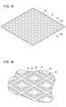
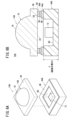
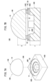
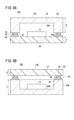
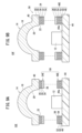
- FIG. 1A is a perspective view of an array member used in manufacturing a transparent sealing member according to a first embodiment
- FIG. 1B is a perspective view of a first metallized layer formed on a joining surface of the array member.
- FIG. 2A is a cross-sectional view of the first metallization layer of FIG. 1B
- FIG. 2B is an explanatory diagram of the singulation process.
- FIG. 3A is an explanatory diagram of a step of attaching a low melting point alloy foil to a first metallization layer
- FIG. 3B is an explanatory diagram of a transparent sealing member having a first metallization layer and a low melting point alloy layer.
- FIG. 4A is an explanatory diagram of a step of bonding the transparent sealing member of FIG.
- FIG. 5A is a plan view of the optical component according to the first embodiment
- FIG. 5B is a cross-sectional view of the optical component of FIG. 5A
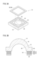
- FIG. 6A is an exploded perspective view of an optical component according to a first modified example of the first embodiment
- FIG. 6B is a cross-sectional view of the optical component of FIG. 6A
- FIG. 7A is an exploded perspective view of an optical component according to a second modified example of the first embodiment
- FIG. 7B is a cross-sectional view of the optical component of FIG. 7A.
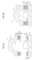
- FIG. 8A is a cross-sectional view of an optical component according to a third modification of the first embodiment
- FIG. 8B is a cross-sectional view of an optical component according to a fourth modification of the first embodiment.
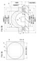
- FIG. 9A is a cross-sectional view of an optical component according to a second embodiment
- FIG. 9B is a cross-sectional view of an optical component according to a third embodiment.
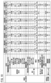
- FIG. 10 is a table showing the configurations of the transparent sealing members and low-melting-point alloy layers of the optical components according to Examples 1 to 5 and Comparative Examples 1 and 2.
- FIG. 10 is a table showing the configurations of the transparent sealing members and low-melting-point alloy layers of the optical components according to Examples 1 to 5 and Comparative Examples 1 and 2.
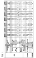
- FIG. 11 is a table showing the relationship between the configuration of the substrate of the optical components according to Examples 1 to 5 and Comparative Examples 1 and 2 and the thickness of the optical components, and the evaluation results of the thermal shock test.
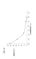
- FIG. 12 is a graph showing the relationship between the thickness of the stress relaxation layer and the peeling occurrence rate in Examples 1 to 5 and Comparative Examples 1 and 2, with the thickness of the stress relaxation layer on the horizontal axis and the peeling occurrence rate on the vertical axis.
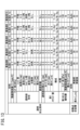
- FIG. 13 is a table showing the configurations of the transparent sealing members and low melting point alloy layers according to Examples 6 to 10.
- FIG. 14 is a table showing the relationship between the configuration of the substrate and the thickness of the optical component according to Examples 6 to 10, and the evaluation results of the thermal shock test.
- FIG. 12 is a graph showing the relationship between the thickness of the stress relaxation layer and the peeling occurrence rate in Examples 1 to 5 and Comparative Examples 1 and 2, with the thickness of the stress relaxation layer on the horizontal axis and the peeling occurrence rate on the vertical axi
- FIG. 15 is a table showing the configurations of the transparent sealing members and low melting point alloy layers according to Examples 11 to 15.
- FIG. 16 is a table showing the relationship between the configuration of the substrate and the thickness of the optical component according to Examples 11 to 15, and the evaluation results of the thermal shock test.
- the optical component 10 according to the first embodiment will be described below together with its manufacturing method.
- the optical component 10 of this embodiment will be described by taking an example in which an ultraviolet light emitting LED is sealed in a transparent sealing member 14 as the optical element 12.
- the optical component 10 is not limited to this, and can also be suitably applied to cases in which a light emitting element such as various LEDs or a light receiving element such as a photodiode is sealed in a transparent sealing member 14.
- the terms top, upper, lower, and downward used in this specification indicate the positional relationship inside the component, and do not limit the installation direction of the optical component 10.
- the array member 16 is a plate-shaped member in which multiple lenses 18 are arranged vertically and horizontally.
- the lenses 18 are parts that allow light to pass through.
- the lenses 18 are not necessarily limited to being hemispherical, and also include flat-shaped windows.
- the array member 16 of this embodiment includes a plurality of lenses 18, and is therefore also called a lens array.
- the array member 16 has a front surface 16a from which the lenses 18 protrude, and a back surface 16b.
- the array member 16 has a concave cavity 20 and a flat bonding surface 22 on the back surface 16b.
- the array member 16 is made of, for example, quartz glass. Details of the manufacturing method of the array member 16 are described, for example, in International Publication WO 2019/012743.
- the joining surface 22 of the array member 16 is polished.
- the unevenness of the joining surface 22 is eliminated by polishing, making it flat.
- less low melting point alloy layer 36 (solder) is required for joining, and the amount of low melting point alloy layer 36 containing Au used can be reduced. Note that polishing of the joining surface 22 can be performed as necessary depending on the unevenness of the joining surface 22, and may be omitted.
- the metallization process is a process of forming a metal pattern (first metallization layer 24) on the joining surface 22, which has excellent wettability with the low melting point alloy layer 36 and adhesion to the transparent sealing member 14.
- the first metallization layer 24 is formed in a rectangular ring shape surrounding the periphery of the cavity 20 of each lens 18.
- the process of forming the first metallization layer 24 includes stacking a first adhesion layer 26, a first diffusion prevention layer 28, a first stress relaxation layer 30, a second diffusion prevention layer 32, and a second adhesion layer 34 in this order on the joining surface 22.
- the first adhesion layer 26 is formed by depositing a metal film such as Ti (titanium) on the joining surface 22, for example, by a sputtering method.
- the first adhesion layer 26 is formed to a thickness of, for example, 0.01 to 0.5 ⁇ m.
- the material of the first adhesion layer 26 is selected from metal materials that have excellent adhesion to quartz glass or ultraviolet-transmitting glass. In addition to Ti, other materials for the first adhesion layer 26 include Cr (chromium).
- the first diffusion prevention layer 28 is formed by depositing a film of Pd (palladium) on the first adhesion layer 26 by a sputtering method.
- the first diffusion prevention layer 28 is formed to a thickness of, for example, 0.01 to 0.5 ⁇ m.
- the first diffusion prevention layer 28 prevents the diffusion of the metal that constitutes the first stress relaxation layer 30.
- the first diffusion prevention layer 28 is preferably made of a material that has excellent adhesion to the first adhesion layer 26 and the first stress relaxation layer 30.
- the first diffusion prevention layer 28 may be composed of a Ni (nickel) film or a Pt (platinum) film.
- the first stress relaxation layer 30 is, for example, made of a Cu (copper) film.
- the first stress relaxation layer 30 is formed, for example, by forming a seed layer by a sputtering method and depositing a Cu (copper) film on the seed layer by a plating method.
- the first stress relaxation layer 30 can be formed to a thickness of, for example, 1.2 ⁇ m or more and 10 ⁇ m or less. Details of the thickness C of the first stress relaxation layer 30 will be described later.
- the first stress relaxation layer 30 is not limited to Cu, and a metal material with a Young's modulus of 150 GPa or less can be used.
- the first stress relaxation layer 30 is preferably made of a material with small thermal expansion, and it is preferable to use a material with a thermal expansion coefficient of 40 ppm/K or less.
- materials for the first stress relaxation layer 30 that can be used instead of Cu include Au, Ag (silver), and Zn (zinc).
- the second diffusion prevention layer 32 is formed by depositing a Ni film (which may be a Pd film or a Pt film) on the first stress relaxation layer 30, for example, by plating.
- the second diffusion prevention layer 32 has a thickness of 0.1 to 5 ⁇ m.
- the second diffusion prevention layer 32 prevents interdiffusion between the second adhesion layer 34 or the low melting point alloy layer 36 (see FIG. 3A) and the first stress relaxation layer 30, thereby preventing deterioration of the first stress relaxation layer 30.
- Pd or Pt may be used instead of Ni for the second diffusion prevention layer 32.
- the second adhesion layer 34 is formed by depositing an Au film on the second diffusion prevention layer 32, for example, by plating.
- the second adhesion layer 34 is formed to a thickness of, for example, 0.1 to 2 ⁇ m.
- the second adhesion layer 34 is formed from a material that has excellent wettability and adhesion with alloys containing Sn (tin) with a low melting point, such as solder.
- the second adhesion layer 34 exhibits high adhesion to the low melting point alloy layer 36 by mixing and integrating with the low melting point alloy layer 36 without forming a boundary.
- the above-mentioned layers from the first adhesion layer 26 to the second adhesion layer 34 are formed over the entire surface of the back surface 16b (see FIG. 1A) of the array member 16. Then, a mask (not shown) of a predetermined shape is formed on the second adhesion layer 34.
- the mask may be formed by applying a photoresist material, exposing it to light, and developing it, or it may be formed by applying a mask material using a printing method. Then, each layer of the first adhesion layer 26 to the second adhesion layer 34 in the portion exposed from the mask is removed by etching, thereby completing the first metallization layer 24 consisting of the annular pattern shown in FIG. 1B.
- a singulation process is performed.
- the array member 16 is cut into individual transparent sealing members 14 by a dicing saw 38.
- the cut transparent sealing members 14 have rectangular base portions 40 formed around the lenses 18 as shown in FIG. 3A.
- the base portions 40 are formed in a flat plate shape.
- the cut transparent sealing members 14 are stored in a tray (not shown) with the bonding surface 22 facing upward.
- low melting point alloy foil 42 is placed on the first metallization layer 24.
- the low melting point alloy foil 42 is shaped in advance so as to overlap at least a portion of the first metallization layer 24.
- the low melting point alloy foil 42 is made of, for example, an AuSn (gold-tin) alloy.
- AuSn gold-tin
- various alloys containing Sn and having a melting point of 450°C or less can be used as the low melting point alloy foil 42.
- the low melting point alloy foil 42 is partially bonded onto the first metallization layer 24 by, for example, dot welding as described in Japanese Patent No. 7182596.
- the bonded low melting point alloy foil 42 forms the low melting point alloy layer 36.
- the substrate 44 has the optical element 12 mounted on its upper surface 44a.
- the optical element 12 is, for example, an ultraviolet light-emitting diode that emits ultraviolet light.
- the substrate 44 is made of, for example, aluminum nitride, alumina, silicon, kovar, or silicon nitride.
- the substrate 44 has, for example, a thermal expansion coefficient of 2.5 ppm/K or more.
- the substrate 44 usually has a thermal expansion coefficient different from that of the transparent sealing member 14.
- the substrate 44 has a second metallization layer 46 at the bonding portion 44b of its upper surface 44a.
- the second metallization layer 46 of this embodiment is formed by laminating a third adhesion layer 48, a third diffusion prevention layer 50, and a fourth adhesion layer 56 in this order on the upper surface 44a of the substrate 44.
- the third adhesion layer 48 is made of a metal film that has excellent adhesion to the substrate 44.
- the third adhesion layer 48 is made of a Cr film (or Ti film) having a thickness of 0.01 to 0.5 ⁇ m, for example. Such a Cr film is formed, for example, by a sputtering method.
- the third diffusion prevention layer 50 is a metal film that prevents diffusion of the fourth adhesion layer 56.
- the third diffusion prevention layer 50 is made of, for example, a Ni film (or a Pd film or Pt film) with a thickness of 0.01 to 0.5 ⁇ m. Such a Ni film is formed by a sputtering method.
- the fourth adhesion layer 56 is a metal film that has excellent wettability and adhesion to the low melting point alloy layer 36.
- the fourth adhesion layer 56 is made of, for example, an Au film with a thickness of 0.1 to 2 ⁇ m.
- the second metallization layer 46 is formed by sequentially depositing the third adhesion layer 48, the third diffusion prevention layer 50, and the fourth adhesion layer 56, and then patterning them by etching using a mask of a predetermined shape.
- the transparent sealing member 14 is placed on the substrate 44.
- the transparent sealing member 14 is positioned so that the first metallization layer 24 is located on top of the second metallization layer 46 of the substrate 44, and is placed on top of the substrate 44.
- the substrate 44 and the transparent sealing member 14 are then heated to a temperature of 200 to 400°C.
- This heating melts the low melting point alloy layer 36, as shown in FIG. 4B, and the second adhesion layer 34 and the fourth adhesion layer 56 become one body.
- This process forms a joint 58 in which the first metallization layer 24 and the second metallization layer 46 are joined together without any gaps through the low melting point alloy layer 36.
- the optical component 10 is completed.
- the substrate 44 is covered with a transparent sealing member 14 when viewed in a plan view.
- the transparent sealing member 14 has a transparent portion 15 and a first metallization layer 24.
- the transparent sealing member 14 may be made of ultraviolet-transmitting glass (borosilicate glass) instead of quartz glass (thermal expansion coefficient 1 ppm/K or less).
- the transparent portion 15 has a hemispherical lens 18 and a rectangular plate-like base portion 40 (also called a flange) formed around the lens 18.
- a hemispherical cavity 20 is formed inside the lens 18.
- the cavity 20 forms a space that houses the optical element 12.
- the first metallization layer 24 is formed on the bonding surface 22 (see FIG. 2A).
- the first metallization layer 24 extends along the periphery of the lens 18 and is formed in a rectangular ring shape, with its corners located below the base 40.
- the thickness of the base 40 is defined as the thickness D of the transparent sealing member 14 above the bonding portion 58.
- a portion of the first metallization layer 24 may overlap the lens 18.
- the outer dimension of the first metallization layer 24 is defined as the outer dimension B of the bonding portion 58.
- the bonding portion 58 has an outer dimension B of, for example, 3 mm or more.
- the transparent sealing member 14 is bonded to the upper surface 44a of the substrate 44 via a bonding portion 58.
- thermal stress is generated in both the optical component 10 and the substrate 44.
- the magnitude of the thermal stress increases according to the difference in the amount of displacement due to thermal expansion between the transparent sealing member 14 and the substrate 44. If the thermal stress is large, cracks and peeling will occur in the relatively fragile transparent sealing member 14, and the seal on the optical element 12 will be broken.
- the amount of displacement between the transparent sealing member 14 and the substrate 44 per 1° C. of temperature change is related to the product (A ⁇ B) of the absolute value A [ppm/K] of the difference between the thermal expansion coefficient of the transparent sealing member 14 and the thermal expansion coefficient of the substrate 44 and the outer dimension B [mm] of the bonding portion 58 (first metallized layer 24). If the value of A ⁇ B exceeds 5 ⁇ 10 ⁇ 6 [mm/K], the transparent sealing member 14 is likely to crack or peel off.
- the optical component 10 has a first stress relief layer 30 on the first metallization layer 24.
- the first stress relief layer 30 relieves thermal stress at the joint 58 by deforming in response to the displacement between the transparent sealing member 14 and the substrate 44.
- the transparent sealing member 14 is thin, some of the thermal stress can be alleviated by the elastic deformation of the transparent sealing member 14, and the thickness C of the first stress relaxation layer 30 can be made thin.
- the thickness D of the transparent sealing member 14 increases, the transparent sealing member 14 becomes difficult to deform, and unless the thickness C of the first stress relaxation layer 30 is increased, cracks and peeling due to thermal stress become more likely to occur.
- the thickness D of the transparent sealing member 14 is 0.2 mm or more, the transparent sealing member 14 becomes more likely to peel or crack. In this case, if the thickness C of the first stress relaxation layer 30 is 0.28% or more of the thickness D of the transparent sealing member 14, cracks and peeling of the transparent sealing member 14 are suppressed.
- the thicker the substrate 44 the less elastically deformable it becomes, so a thicker first stress relaxation layer 30 is required. If the thickness of the substrate 44 below the joint 58 is defined as the thickness F of the substrate 44, it is preferable to set the thickness C of the first stress relaxation layer 30 to 0.25% or more of the thickness F of the substrate 44, as this can prevent cracks and peeling of the transparent sealing member 14.
- the thickness C of the first stress relaxation layer 30 is set to 0.05% or more of the thickness E of the optical component 10, which is the sum (D+F) of the thickness D of the transparent sealing member 14 and the thickness F of the substrate 44.
- the optical component 10A shown in Figures 6A and 6B differs from the optical component 10 in Figure 4B in a transparent sealing member 14A and a substrate 44A.
- the same components as those in the optical component 10 in Figure 4B are denoted by the same reference numerals, and detailed descriptions thereof will be omitted.
- the transparent sealing member 14A has a hemispherical lens 18 and a rectangular base portion 40 provided around the lens 18. As shown in FIG. 6B, the lens 18 does not have a cavity 20 formed therein, and is filled with quartz glass. The entire bottom side of the transparent sealing member 14A is composed of a flat bonding surface 22.
- the substrate 44A has a box-shaped cavity 60 on its upper surface 44a.
- the cavity 60 is formed in a rectangular shape in a plan view.
- the cavity 60 houses the optical element 12.
- the optical element 12 is bonded to the substrate 44A within the cavity 60.
- a second metallization layer 46 is formed on the upper surface 44a of the substrate 44A.
- the second metallization layer 46 is formed in a rectangular ring shape so as to surround the cavity 60.
- the second metallization layer 46 is configured in the same manner as the second metallization layer 46 described with reference to FIG. 4A.
- This modified example also prevents cracks and peeling of the transparent sealing member 14A.
- the transparent sealing member 14B is composed of a hemispherical lens 18.
- the transparent sealing member 14B does not have a plate-shaped pedestal portion 40 around the lens 18.
- the lens 18 does not have a cavity 20 inside, and the inside is filled with quartz glass.
- the bottom of the transparent sealing member 14B is formed by a flat joint surface 22.
- the transparent sealing member 14B has a circular first metallization layer 24B on the joint surface 22.
- the configuration of each layer of the first metallization layer 24B is the same as that of the first metallization layer 24 described with reference to Figure 2A.
- a low melting point alloy layer 36 is formed on the first metallization layer 24B.
- the substrate 44B has a cavity 60B, a lens accommodating recess 62, and a second metallization layer 46B.
- the cavity 60B is formed in a cylindrical shape.
- the cavity 60B accommodates the optical element 12.
- the diameter of the cavity 60B is smaller than the inner diameter of the first metallization layer 24B of the transparent sealing member 14B.
- the lens accommodating recess 62 is a recess formed on the outer periphery of the cavity 60B and is formed shallower than the cavity 60B.
- the lens accommodating recess 62 is formed slightly larger than the outer diameter of the transparent sealing member 14B and accommodates the transparent sealing member 14B.
- the second metallization layer 46B is formed on the bottom surface of the lens accommodating recess 62.
- the configuration of each layer of the second metallization layer 46B is the same as that of the second metallization layer 46 described with reference to FIG. 4A.
- the transparent sealing member 14B is arranged so that the first metallization layer 24B faces the second metallization layer 46B of the lens accommodating recess 62.
- the first metallization layer 24B and the second metallization layer 46B are joined by the low melting point alloy layer 36 to form a joint 58.
- the thickness of the transparent sealing member 14B above the joint 58 is defined as the thickness D of the transparent sealing member 14B above the center in the width direction of the first metallization layer 24B.
- the thickness C of the first stress relaxation layer 30 is preferably set to 0.28% or more of the thickness D of the transparent sealing member 14B.
- This modified example also prevents cracks and peeling of the transparent sealing member 14B.
- optical component 10C of this modified example differs from optical component 10 shown in Fig. 4B in that it has a flat transparent sealing member 14C.
- optical component 10C the same components as those of optical component 10 in Fig. 4B are denoted by the same reference numerals, and detailed descriptions thereof will be omitted.
- the transparent sealing member 14C has a lens 18 formed in a flat plate shape.
- the lens 18 is integrated with the base portion 40.
- the transparent sealing member 14C is formed in a rectangular shape with the same dimensions as the substrate 44 in a plan view.
- the transparent sealing member 14C has a cavity 20C and a first metallization layer 24.
- the cavity 20C is formed in a rectangular shape in a plan view.
- the cavity 20C accommodates the optical element 12 mounted on the substrate 44.
- the first metallization layer 24 is formed in a rectangular ring shape surrounding the outside of the cavity 20C.
- the first metallization layer 24 is formed on the joining surface 22 of the transparent sealing member 14C and is joined to the second metallization layer 46 of the substrate 44 via the low melting point alloy layer 36.
- each layer of the first metallization layer 24 and the second metallization layer 46 is the same as that of the first metallization layer 24 and the second metallization layer 46 of the first embodiment.
- This modified example also prevents cracks and peeling of the transparent sealing member 14C.
- optical component 10D of this modification differs from optical component 10 shown in Fig. 4B in that it has a flat transparent sealing member 14D.
- optical component 10D the same components as those of optical component 10 in Fig. 4B are denoted by the same reference numerals, and detailed descriptions thereof will be omitted.
- the transparent sealing member 14D is formed in a flat plate shape and is rectangular in shape with the same dimensions as the substrate 44D in a plan view. No cavity 20 is formed in the transparent sealing member 14D, and a cavity 60D is formed in the substrate 44D.
- the cavity 60D in the substrate 44D is rectangular in a plan view, and the substrate 44D is box-shaped.
- the optical element 12 is mounted in the cavity 60D in the substrate 44D.
- the transparent sealing member 14D is made of flat UV-transmitting glass or flat quartz glass.
- the transparent sealing member 14D has a first metallization layer 24 formed in a rectangular ring shape surrounding the cavity 60D of the substrate 44D.
- the first metallization layer 24 is bonded to the second metallization layer 46 of the substrate 44D via the low-melting-point alloy layer 36.
- This modified example also prevents cracks and peeling of the transparent sealing member 14D.
- the optical component 10E of this embodiment has a second stress relief layer 52 on the second metallization layer 46E of the substrate 44, and a first stress relief layer 30 is not provided on the first metallization layer 24E of the transparent sealing member 14.
- the transparent sealing member 14 has a first metallized layer 24E formed on the joining surface 22.
- the first metallized layer 24E has a structure in which a first adhesion layer 26, a first diffusion prevention layer 28, and a second adhesion layer 34 are laminated in this order on the joining surface 22.
- the first adhesion layer 26 is made of a Ti film or a Cr film having a thickness of 0.01 to 0.5 ⁇ m.
- the first diffusion prevention layer 28 is made of a Pd film, a Pt film, or a Ni film having a thickness of 0.01 to 0.5 ⁇ m.
- the second adhesion layer 34 is made of an Au film having a thickness of 0.1 to 2 ⁇ m.
- the low melting point alloy layer 36 is made of an AuSn alloy film having a thickness of 20 ⁇ m.
- the substrate 44 has an optical element 12 mounted on its upper surface 44a.
- a ring-shaped second metallization layer 46E is formed on the upper surface 44a of the substrate 44, surrounding the optical element 12.
- the second metallization layer 46E has a structure in which a third adhesion layer 48, a third diffusion prevention layer 50, a second stress relief layer 52, a fourth diffusion prevention layer 54, and a fourth adhesion layer 56 are formed in this order on the upper surface 44a of the substrate 44.
- the third adhesion layer 48 is made of a Ti film (or a Cr film) having a thickness of 0.01 to 0.5 ⁇ m.
- the third diffusion prevention layer 50 is made of a Pd film (which may be a Ni film or a Pt film) having a thickness of 0.01 to 0.5 ⁇ m.
- the third adhesion layer 48 and the third diffusion prevention layer 50 are formed, for example, by a sputtering method.
- the second stress relief layer 52 is made of a metal (e.g., Cu) film with a Young's modulus of 150 GPa or less.
- the second stress relief layer 52 is formed to a thickness of 1.2 ⁇ m or more.
- the thickness of the second stress relief layer 52 may be the same as the thickness of the first stress relief layer 30 described in the first embodiment.
- the fourth diffusion prevention layer 54 is made of a Ni film (or a Pd or Pt film) with a thickness of 0.1 to 5 ⁇ m.
- the fourth adhesion layer 56 is made of an Au film with a thickness of 0.1 to 2 ⁇ m.
- the second stress relaxation layer 52, the fourth diffusion prevention layer 54, and the fourth adhesion layer 56 are formed by plating.
- the transparent sealing member 14 is bonded to the substrate 44 via the first metallization layer 24E, the second metallization layer 46E, and the low melting point alloy layer 36.
- the second stress relaxation layer 52 provided on the second metallization layer 46E can relieve the thermal stress at the joint 58, preventing cracks and peeling of the transparent sealing member 14.
- the optical component 10F of this embodiment has a first metallized layer 24 formed on the bonding surface 22 of the transparent sealing member 14.
- the optical component 10F also has a second metallized layer 46E on the substrate 44.
- the first stress relaxation layer 30 is formed on the first metallized layer 24 (see FIG. 2A).
- the second stress relaxation layer 52 is formed on the second metallized layer 46E (see FIG. 9A). Therefore, the optical component 10F has the first stress relaxation layer 30 and the second stress relaxation layer 52 at the bonding portion 58.
- the other configurations of the first metallized layer 24 are the same as those of the first metallized layer 24 of the first embodiment described with reference to FIG. 2A.
- the other configurations of the second metallized layer 46E are the same as those of the second metallized layer 46E described with reference to FIG. 9A.
- the low melting point alloy layer 36 is formed on the second metallization layer 46E.
- the configuration of the low melting point alloy layer 36 is similar to that of the low melting point alloy layer 36 described with reference to Figures 3A and 3B.
- the sum of the thicknesses of the first stress relaxation layer 30 and the second stress relaxation layer 52 may be 1.2 ⁇ m or more.
- the first stress relaxation layer 30 and the second stress relaxation layer 52 can relax the thermal stress of the bonding portion 58, so that cracks and peeling of the transparent sealing member 14 can be prevented.
- the optical components 10, 10A to 10F of the above-mentioned embodiments were fabricated and evaluated, and the results are described below.
- the fabricated optical components 10, 10A to 10F were subjected to dimensional measurements of each part using a measuring microscope and a SEM (scanning electron microscope). If necessary, the optical component 10 was subjected to cross-sectional processing.
- the material and composition were measured using an EDS attached to the SEM (scanning electron microscope).
- the thermal expansion coefficient and Young's modulus are values in a bulk state.
- the peeling occurrence rate of the transparent sealing member 14 was evaluated by carrying out a thermal shock test. This thermal shock test was carried out by mounting the optical component 10 on an aluminum heat dissipation substrate, applying a thermal cycle of -40°C to +85°C, and observing the presence or absence of peeling with the naked eye or an optical microscope.
- Example 1 is a case where the first stress relaxation layer 30 is not formed, and the thickness of the first stress relaxation layer 30 is 0 ⁇ m.
- Comparative Example 2 and Examples 1 to 4 the thickness of the first stress relaxation layer 30 varies in the range of 0.5 ⁇ m to 9.2 ⁇ m.
- Example 5 is the optical component 10E shown in FIG. 9A, but is similar to Examples 1 to 4 except for the bonding portion 58.
- a second stress relaxation layer 52 made of Cu and having a thickness of 8.3 ⁇ m is provided together with a first stress relaxation layer 30 having a thickness of 1.2 ⁇ m.
- the peeling occurrence rate of the transparent sealing member 14 was 32%.
- the peeling occurrence rate of the transparent sealing member 14 showed a tendency to decrease as the thickness of the first stress relaxation layer 30 or the second stress relaxation layer 52 (hereinafter collectively referred to as the stress relaxation layer) increased.
- the stress relaxation layer it can be seen that when the thickness of the stress relaxation layer is in the range of less than 1.2 ⁇ m, the peeling occurrence rate of the transparent sealing member 14 increases sharply. Therefore, it was confirmed that if the thickness of the stress relaxation layer is in the range of 1.2 ⁇ m or more, the peeling occurrence rate of the transparent sealing member 14 can be suppressed to 6% or less.
- Examples 6, 8, 11, and 13 are the results of evaluating the optical component 10 shown in Figures 5A and 5B.
- the thickness of the first stress relaxation layer 30 is 3.0 ⁇ m, similar to Example 1 ( Figures 13 and 15).
- Example 6 is different from Example 1 in that the thickness D of the base portion 40 of the transparent sealing member 14 is increased to 0.5 mm, as shown in Figure 13.
- the peeling occurrence rate is within 2%, which is an improvement over the peeling occurrence rates of Comparative Examples 1 and 2.
- Example 8 differs from Example 1 in that the dimensions of the transparent sealing member 14 are increased.
- the outer dimension B of the first metallization layer 24 (joint 58) is 3.9 mm.
- the peeling rate of the transparent sealing member 14 in Example 8 only increased slightly to 4%. The peeling rate in Example 8 was improved over the peeling rates in Comparative Examples 1 and 2.
- Example 11 differs from Example 1 in that alumina is used for the substrate 44.
- the thermal expansion coefficient of alumina is 7 ppm/K, which is greater than the thermal expansion coefficient of aluminum nitride in Example 1, 4.6 ppm/K. Therefore, the joint 58 is more susceptible to the stress caused by thermal expansion.
- the peeling occurrence rate was kept at 6%, which was an improvement over the peeling occurrence rates in Comparative Examples 1 and 2.
- Example 13 like Example 11, alumina was used for the substrate 44.
- Example 13 differs from Example 11 in that Au, which has a smaller Young's modulus than Cu, was used as the material for the first stress relaxation layer 30, as shown in FIG. 15. As shown in FIG. 16, Example 13 had a peeling occurrence rate of 0%, which was an improvement over Example 11.
- Example 7 shown in Fig. 13 is a test and evaluation result for the optical component 10A shown in Fig. 6A and Fig. 6B.
- the transparent sealing member 14A does not have a cavity 20, so the transparent sealing member 14A is less likely to deform. Therefore, in Example 7, it is difficult to obtain the effect of relaxing the thermal stress caused by the deformation of the transparent sealing member 14A.
- the peeling occurrence rate is only 4% due to the effect of the first stress relaxation layer 30, which is an improvement over the peeling occurrence rates of Comparative Examples 1 and 2.
- Examples 9 and 10 shown in Fig. 13 are test and evaluation results for the optical component 10C shown in Fig. 8A.
- Fig. 14 in Example 9, aluminum nitride with a thermal expansion coefficient of 4.6 ppm/K was used for the substrate 44, and in Example 10, silicon with a thermal expansion coefficient of 2.6 ppm/K was used for the substrate 44.
- the peeling occurrence rate was 6%.
- Example 10 in which the difference in the thermal expansion coefficient between the substrate 44 and the transparent sealing member 14 was small, the peeling occurrence rate was 0%.
- the peeling occurrence rate was also improved compared to Comparative Examples 1 and 2.
- Example 12 shown in Fig. 15 shows the test and evaluation results for optical component 10B shown in Fig. 7A and Fig. 7B.
- Optical component 10B does not have a base portion 40.
- the peeling occurrence rate is 0%, and the peeling occurrence rate can be suppressed more than in Comparative Examples 1 and 2.
- Examples 14 and 15 shown in Fig. 15 are test and evaluation results for the optical component 10D shown in Fig. 8B.
- quartz glass was used for the transparent sealing member 14, and aluminum nitride was used for the substrate 44.
- ultraviolet-transmitting glass borosilicate glass
- alumina was used for the substrate 44.
- the peeling occurrence rate was 4%, and in Example 15, the peeling occurrence rate was 0%. Therefore, Examples 14 and 15 can suppress the peeling occurrence rate more than Comparative Examples 1 and 2.
Landscapes
- Led Device Packages (AREA)
- Light Receiving Elements (AREA)
Abstract
光学素子(12)を搭載した基板(44)に透明封止部材(14)を接合して封止する光学部品(10)と、透明封止部材(14)と、基板(44)と、光学部品(10)の製造方法とに関し、透明封止部材(14)と基板(44)とを接合するメタライズ層(24、46)に、ヤング率が150GPa以下の金属膜によって構成され、厚さの総和が1.2μm以上の1又は複数の応力緩和層(30)と、応力緩和層(30)の厚さ方向の両側に配置され、応力緩和層(30)を構成する金属の拡散を阻止する拡散防止層(28、32)と、を設ける。
Description
本発明は、光学部品、透明封止部材、基板、及び光学部品の製造方法に関する。
発光デバイス又は光センサ等の光学部品は、光学素子を搭載した基板に透明封止部材を接合して、光学素子を透明封止部材で封止した構造を有する。光学素子は、発光素子(例えば、LED等)又は受光素子(例えば、フォトダイオード)である。透明封止部材は、ガラスであり、ハンダ等の低融点合金を用いて基板に接合される。
特開2021-118199号公報は、石英ガラスよりなる透明封止部材と、基板とをハンダで接合するために、石英ガラス及び実装基板とにメタライズ層を設ける技術を開示する。
特開2019-046826号公報は、石英ガラスからなる透明封止部材と、基板との接合部分に関し、熱膨張による透明封止部材のクラック発生を防ぐために、厚さ0.3μm~10μmのAu(金)膜を応力緩和層として設ける技術を開示する。
光学部品は、使用環境下において発光素子の発熱による高温に曝される場合がある。また、光学部品の実装のためのリフロー工程では、例えば、200℃~400℃といった高温に曝されることがある。このため、透明封止部材と基板との接合部には、両者の熱膨張係数の差によって熱応力が発生し、脆弱な透明封止部材に、亀裂又は剥離が生じ、光学素子の封止が破れるおそれがある。
特開2021-118199号公報のメタライズ層では、十分な応力緩和効果が得られない可能性がある。
特開2019-046826号公報の応力緩和層はAuよりなるが、それに隣接するSn(スズ)を含む低融点合金(ハンダ)との相互拡散により、応力緩和層が劣化し、十分な応力緩和効果が得られない可能性がある。
本発明は、上記した課題を解決することを目的とする。
本発明の態様を以下に例示する。
[項目1]
本発明の一態様は、光学部品に関し、光学素子を搭載した基板と、前記基板の上方に接合され、前記光学素子を封止する透明封止部材と、複数の金属膜が積層され、前記透明封止部材と前記基板とを接合する接合部と、を備え、前記接合部は、ヤング率が150GPa以下の金属膜によって構成され、厚さの総和が1.2μm以上の1又は複数の応力緩和層と、前記応力緩和層の厚さ方向の両側に配置され、前記応力緩和層を構成する金属の拡散を阻止する拡散防止層と、を有する。
上記の光学部品は、応力緩和層の劣化を拡散防止層で防止でき、十分な応力緩和層が維持されるため、熱応力による透明封止部材の剥離又は損傷を効果的に抑制できる。
[項目2]
項目1記載の光学部品であって、前記応力緩和層は、Cu(銅)、Au(金)、Ag(銀)、又はZn(亜鉛)でもよい。この光学部品は、熱衝撃による透明封止部材の剥離や損傷を防止できる。
[項目3]
項目1又は2記載の光学部品であって、前記拡散防止層は、Ni(ニッケル)、Pd(パラジウム)、又はPt(白金)でもよい。この光学部品は、応力緩和層の劣化を防止でき、透明封止部材の剥離や損傷を防止できる。
[項目4]
項目1~3のいずれか1項に記載の光学部品であって、前記応力緩和層は、熱膨張係数が40ppm/K以下でもよい。このような応力緩和層は、応力緩和層自身の熱変形による熱応力の発生を抑制できる。
[項目5]
項目1~4のいずれか1項に記載の光学部品であって、前記応力緩和層の厚さの総和が10μm以下であってもよい。
[項目6]
項目1~5のいずれか1項に記載の光学部品であって、前記応力緩和層の厚さの総和は、前記応力緩和層の上方の前記透明封止部材の厚さの0.28%以上であってもよい。この光学部品は、応力緩和層が十分な厚みで形成されるため、透明封止部材と基板との熱応力を緩和できる。
[項目7]
項目1~6のいずれか1項に記載の光学部品であって、前記応力緩和層の上方の前記透明封止部材の厚さが0.2mm以上であってもよい。透明封止部材の厚みが増すと、透明封止部材が撓みにくくなり、熱応力が高くなる傾向がある。この光学部品は、厚い透明封止部材であっても、熱応力を緩和でき、透明封止部材の剥離や損傷を防止できる。
[項目8]
項目1~7のいずれか1項に記載の光学部品であって、前記応力緩和層の厚さの総和は、前記応力緩和層の下方の部分の前記基板の厚さの0.25%以上でもよい。この光学部品は、応力緩和層が十分な厚みで形成されるため、透明封止部材と基板との熱応力を緩和できる。
[項目9]
項目1~8のいずれか1項に記載の光学部品であって、前記応力緩和層の厚さの総和は、前記応力緩和層の上方の前記透明封止部材の厚さと前記応力緩和層の下方の前記基板の厚さとを加算した値に対して0.05%以上でもよい。この光学部品は、応力緩和層が十分な厚みで形成されるため、透明封止部材と基板との熱応力を緩和できる。
[項目10]
項目1~9のいずれか1項に記載の光学部品であって、前記透明封止部材の熱膨張係数と前記基板の熱膨張係数との差をA(ppm/K)とし、前記接合部の外寸をB(mm)としたときに、A×Bの値が5×10-6mm/K以上でもよい。
[項目11]
項目10記載の光学部品であって、前記接合部の外寸が3mm以上でもよい。この光学部品は、発光ダイオードの一般的なサイズを有する透明封止部材に対しても、その剥離や損傷を防止できる。
[項目12]
項目1~11のいずれか1項に記載の光学部品であって、前記透明封止部材が石英ガラス又は紫外線透過ガラスであってもよい。この光学部品は、紫外線発光ダイオード又は紫外線受光素子等の強度が弱い上記の透明封止部材の剥離や損傷を防止できる。
[項目13]
項目12記載の光学部品であって、前記透明封止部材は、熱膨張係数が1ppm/K以下であってもよい。
[項目14]
項目1~13のいずれか1項に記載の光学部品であって、前記基板は、窒化アルミニウム、アルミナ、シリコン、コバール及び窒化ケイ素のいずれかでよい。
[項目15]
項目14記載の光学部品であって、前記基板は、熱膨張係数が2.5ppm/K以上でもよい。
[項目16]
項目1~15のいずれか1項に記載の光学部品であって、前記応力緩和層の下方の前記基板の厚さが0.2mm以上であってもよい。
[項目17]
項目1~16のいずれか1項に記載の光学部品であって、前記接合部は、前記透明封止部材の前記基板を向く接合面の上に形成され、複数の金属膜よりなる第1メタライズ層と、前記基板の上に形成され、複数の金属膜よりなる第2メタライズ層と、前記第1メタライズ層と前記第2メタライズ層とを接合する低融点合金層と、を備え、前記応力緩和層及び前記拡散防止層は、前記第1メタライズ層と前記第2メタライズ層との少なくとも一方に設けられてもよい。この光学部品は、低融点合金層による密着性と、熱応力の緩和性能とを両立できる。
[項目18]
項目17記載の光学部品であって、前記応力緩和層及び前記拡散防止層は、前記第1メタライズ層と前記第2メタライズ層との両方に夫々設けられてもよい。この光学部品は、透明封止部材と基板との熱応力を緩和できる。
[項目19]
本実施形態の別の一態様は、光学素子を搭載した基板に接合され、前記光学素子を封止する透明封止部材であって、前記光学素子を覆うレンズと、前記レンズの周縁部に設けられ、前記基板に接合される接合面と、前記接合面の上に形成された第1メタライズ層と、を備え、前記第1メタライズ層は、ヤング率が150GPa以下の金属膜によって構成され、厚さが1.2μm以上の応力緩和層と、前記応力緩和層の厚さ方向の両側に配置され、前記応力緩和層を構成する金属の拡散を阻止する拡散防止層と、を有する。この透明封止部材は、拡散防止層の劣化を防ぎつつ、拡散防止層で基板との熱応力を緩和できる。
[項目20]
項目19記載の透明封止部材は、さらに、前記第1メタライズ層の上に形成された低融点合金層を有してもよい。この透明封止部材は、予め低融点合金層を備えるため、基板への接合工程を簡略化できる。
[項目21]
本発明のさらに別の一態様は、光学素子を搭載する基板であって、前記光学素子を搭載する部分の外周部に位置し、透明封止部材が接合される上面と、前記上面の上に形成された第2メタライズ層と、を備え、前記第2メタライズ層は、ヤング率が150GPa以下の金属膜によって構成され、厚さが1.2μm以上の応力緩和層と、前記応力緩和層の厚さ方向の両側に配置され、前記応力緩和層を構成する金属の拡散を阻止する拡散防止層と、を有する。この基板は、拡散防止層の劣化を防ぎつつ、拡散防止層で基板との熱応力を緩和できるため、接合された透明封止部材の剥離や損傷を防止できる。
[項目22]
本発明のさらに別の一態様は、基板に実装された光学素子を透明封止部材で封止した光学部品の製造方法であって、前記透明封止部材の第1メタライズ層と、前記基板の第2メタライズ層とを低融点合金で接合する工程を有し、前記第1メタライズ層及び前記第2メタライズ層の少なくとも一方に、ヤング率が150GPa以下の金属膜によって構成され、厚さの総和が1.2μm以上の1又は複数の応力緩和層と、前記応力緩和層の厚さ方向の両側に配置され、前記応力緩和層を構成する金属の拡散を阻止する拡散防止層と、を有する。この光学部品の製造方法は、透明封止部材の剥離や損傷を防止できる。
上記の、光学部品、透明封止部材、基板、及び光学部品の製造方法は、熱応力による透明封止部材の剥離又は損傷を防止できる。
(第1実施形態)
以下、第1実施形態に係る光学部品10が、その製造方法とともに説明される。本実施形態の光学部品10は、光学素子12として、紫外発光LEDを透明封止部材14で封止する例で説明が行われる。ただし、光学部品10は、これに限定されず、各種LED等の発光素子又はフォトダイオード等の受光素子を透明封止部材14で封止する場合にも好適に応用できる。本明細書中で使用される上、上方、下及び下方との用語は、部材内部の配置関係を示すものであり、光学部品10の設置方向を限定するものではない。
以下、第1実施形態に係る光学部品10が、その製造方法とともに説明される。本実施形態の光学部品10は、光学素子12として、紫外発光LEDを透明封止部材14で封止する例で説明が行われる。ただし、光学部品10は、これに限定されず、各種LED等の発光素子又はフォトダイオード等の受光素子を透明封止部材14で封止する場合にも好適に応用できる。本明細書中で使用される上、上方、下及び下方との用語は、部材内部の配置関係を示すものであり、光学部品10の設置方向を限定するものではない。
まず、図1A~図3Bを参照しつつ、光学部品10の透明封止部材14の製造について説明が行われる。透明封止部材14の製造工程では、まず、図1Aに示されるようなアレイ部材16が用意される。アレイ部材16は、複数のレンズ18が縦方向及び横方向に連なった板状の部材である。なお、本明細書において、レンズ18は、光を通す部分である。レンズ18は、必ずしも半球状に限定されるものではなく、平板状の窓も含む。
本実施形態のアレイ部材16は、複数のレンズ18を含むため、レンズアレイとも呼ばれる。アレイ部材16は、レンズ18が突出した表面16aと、裏面16bとを有する。本実施形態では、アレイ部材16は、裏面16bに凹状のキャビティ20と平坦な接合面22とを有する。アレイ部材16は、例えば、石英ガラスによって構成される。アレイ部材16の製造方法の詳細は、例えば、国際公開2019/012743号に記載されている。
次に、アレイ部材16の接合面22に対する研磨が行われる。研磨により接合面22の凹凸が消失して平坦化される。接合面22が平坦化されると、接合に必要とされる低融点合金層36(ハンダ)が少なくて済み、Auを含む低融点合金層36の使用量を削減できる。なお、接合面22の研磨は、接合面22の凹凸に応じて必要に応じて行われればよく、省略されてもよい。
次に、図1Bに示されるように、接合面22のメタライズ化工程が行われる。メタライズ化工程は、接合面22の上に、低融点合金層36との濡れ性及び透明封止部材14との密着性に優れた金属パターン(第1メタライズ層24)を形成する工程である。第1メタライズ層24は、図示のように、各レンズ18のキャビティ20の周囲を囲む矩形の環状に形成される。
図2Aに示されるように、第1メタライズ層24を形成する工程は、接合面22の上に、第1密着層26と、第1拡散防止層28と、第1応力緩和層30と、第2拡散防止層32と、第2密着層34と、をこの順で積層する工程を含む。第1密着層26は、接合面22の上に、例えばスパッタ法により、Ti(チタン)等の金属膜を成膜して形成される。第1密着層26は、厚さが例えば0.01~0.5μmの厚さに形成される。第1密着層26の材料は、石英ガラス又は紫外線透過ガラスとの密着性に優れた金属材料から選択される。第1密着層26の材料としては、Ti以外にCr(クロム)が挙げられる。
第1拡散防止層28は、第1密着層26の上に、スパッタ法により、Pd(パラジウム)を成膜して形成される。第1拡散防止層28は、例えば厚さ0.01~0.5μmに形成される。第1拡散防止層28は、第1応力緩和層30を構成する金属の拡散を阻止する。第1拡散防止層28は、第1密着層26及び第1応力緩和層30との密着性に優れた材料を用いることが好ましい。第1拡散防止層28は、Ni(ニッケル)膜又はPt(白金)膜で構成されてもよい。
第1応力緩和層30は、例えば、Cu(銅)膜によって構成される。このような第1応力緩和層30は、例えば、スパッタ法によりシード層を形成し、そのシード層にメッキ法でCu(銅)膜を堆積させて形成される。特に限定されないが、第1応力緩和層30は、例えば1.2μm以上10μm以下の厚さに形成され得る。第1応力緩和層30の厚みCの詳細は、後述される。なお、第1応力緩和層30は、Cuに限定されず、ヤング率が150GPa以下の金属材料を使用できる。また、第1応力緩和層30は、熱膨張が小さい材料が好ましく、熱膨張係数が40ppm/K以下の材料を用いることが好ましい。Cuに変わる第1応力緩和層30の材料としては、例えば、Au、Ag(銀)、Zn(亜鉛)等が挙げられる。
第2拡散防止層32は、第1応力緩和層30の上に、例えばメッキ法によりNi膜(Pd膜又はPt膜でもよい)を堆積させて形成される。第2拡散防止層32は、0.1~5μmの厚さを有する。第2拡散防止層32は、第2密着層34又は低融点合金層36(図3A参照)と第1応力緩和層30との相互拡散を阻止することで、第1応力緩和層30の劣化を阻止する。第2拡散防止層32には、Niの代わりにPd又はPtが用いられてもよい。
第2密着層34は、第2拡散防止層32の上に、例えばメッキ法によりAu膜を堆積させて形成される。第2密着層34は、例えば、厚さ0.1~2μmに形成される。第2密着層34は、ハンダ等の低融点のSn(錫)を含む合金との濡れ性及び密着性に優れた材料によって形成される。第2密着層34は、低融点合金層36と境目を形成することなく混合して一体化することで、低融点合金層36に対して高い密着力を発揮する。
以上の第1密着層26から第2密着層34の各層は、アレイ部材16の裏面16b(図1A参照)の全面に形成される。その後、第2密着層34の上に、所定形状のマスク(図示せず)が形成される。マスクは、フォトレジスト材料の塗布と、露光及び現像によって形成されてもよいし、マスク材料を印刷法で塗布して形成されてもよい。その後、マスクから露出している部分の第1密着層26から第2密着層34の各層をエッチングによって除去することにより、図1Bに示される環状のパターンよりなる第1メタライズ層24が完成する。
次に、図2Bに示されるように、個片化工程が行われる。個片化工程では、アレイ部材16が、ダイシングソー38によって、個々の透明封止部材14に切り分けられる。切り分けられた透明封止部材14は、図3Aに示されるように、レンズ18の周囲に矩形状の台座部40が形成される。台座部40は、平板状に形成される。切り分けられた透明封止部材14は、図示しないトレーに、接合面22を上に向けた状態で収容される。
次に、図3Aに示されるように、第1メタライズ層24の上に低融点合金箔42が載置される。低融点合金箔42は、予め第1メタライズ層24の少なくとも一部と重なる形状に整形されている。低融点合金箔42は、例えば、AuSn(金錫)合金よりなる。低融点合金箔42は、AuSn合金以外にも、Snを含む融点450℃以下の各種合金を使用することができる。
その後、図3Bに示されるように、低融点合金箔42は、例えば特許第7182596号公報に記載されたドット溶着により、部分的に第1メタライズ層24の上に接合される。接合された低融点合金箔42により、低融点合金層36が形成される。以上の工程により、透明封止部材14が完成する。
次に、図4A~図4Bに示されるように、透明封止部材14を基板44に接合する工程が行われる。図4Aに示されるように、基板44は、上面44aに光学素子12を搭載する。光学素子12は、例えば紫外線を放出する紫外発光ダイオードである。基板44は、例えば、窒化アルミニウム、アルミナ、シリコン、コバール又は窒化ケイ素よりなる。基板44は、例えば、2.5ppm/K以上の熱膨張係数を有する。基板44は、通常、透明封止部材14と異なる熱膨張係数を有する。基板44は、その上面44aの接合部位44bに、第2メタライズ層46を有する。
本実施形態の第2メタライズ層46は、基板44の上面44aに、第3密着層48と、第3拡散防止層50と、第4密着層56とがこの順に積層されて構成される。第3密着層48は、基板44との密着性に優れた金属膜よりなる。第3密着層48は、例えば、厚さが0.01~0.5μmのCr膜(又はTi膜)よりなる。このようCr膜は、例えばスパッタ法により形成される。
第3拡散防止層50は、第4密着層56の拡散を阻止する金属膜である。第3拡散防止層50は、例えば、厚さが0.01~0.5μmのNi膜(Pd膜又はPt膜でもよい)よりなる。このようなNi膜はスパッタ法により形成される。
第4密着層56は、低融点合金層36との濡れ性及び密着性に優れた金属膜である。第4密着層56は、例えば、厚さが0.1~2μmのAu膜よりなる。
以上の第2メタライズ層46は、第3密着層48と、第3拡散防止層50と、第4密着層56とを順に成膜し、その後、所定形状のマスクを用いたエッチングでパターニングすることで形成される。
次に、基板44の上に透明封止部材14が配置される。透明封止部材14は、第1メタライズ層24が基板44の第2メタライズ層46の上に位置するように位置決めされて、基板44の上に載置される。その後、基板44及び透明封止部材14が、200~400℃の温度に加熱される。
この加熱によって、図4Bに示されるように、低融点合金層36が溶融し、第2密着層34と第4密着層56とが一体化する。この工程により、低融点合金層36を通じて第1メタライズ層24と第2メタライズ層46とが隙間なく接合された接合部58が形成される。以上の工程により、光学部品10が完成する。
図5Aに示されるように、本実施形態の光学部品10は、平面視した状態で、基板44が透明封止部材14で覆われる。透明封止部材14は、透明部15と、第1メタライズ層24と、を有する。透明封止部材14は、石英ガラス(熱膨張係数1ppm/K以下)の代わりに紫外線透過ガラス(ホウケイ酸ガラス)で構成されてもよい。透明部15は、半球状のレンズ18と、レンズ18の周囲に形成された矩形の板状の台座部40(フランジとも呼ばれる)とを有する。図5Bに示されるように、レンズ18の内部には、半球状のキャビティ20が形成されている。キャビティ20は、光学素子12を収容する空間を形成する。
図5Aに示されるように、第1メタライズ層24は、接合面22(図2A参照)の上に形成されている。第1メタライズ層24は、レンズ18の周縁部に沿って延在し、矩形の環状に形成されており、その角部は、台座部40の下方に位置する。本実施形態において、台座部40の厚さが、透明封止部材14の接合部58上の厚みDと定義される。第1メタライズ層24の一部は、レンズ18と重なってもよい。第1メタライズ層24の外寸は、接合部58の外寸Bと定義される。接合部58は、例えば、3mm以上の外寸Bを有する。
図5Bに示されるように、透明封止部材14は、接合部58を介して基板44の上面44aに接合されている。光学部品10は、基板44と透明封止部材14との接合の際の温度変化によって、両者に熱応力が発生する。熱応力の大きさは、透明封止部材14と基板44との熱膨張による変位量の差に応じて増大する。熱応力が大きいと、相対的に脆弱な透明封止部材14にクラックや剥離が発生し、光学素子12の封止が破れる。
透明封止部材14と基板44との温度変化1℃当たりの変位量は、透明封止部材14の熱膨張係数と基板44の熱膨張係数との差の絶対値A[ppm/K]と、接合部58(第1メタライズ層24)の外寸B[mm]との積(A×B)に関連付けられる。A×Bの値が、5×10-6[mm/K]を超える場合には、透明封止部材14にクラックや剥離が発生しやすくなる。
透明封止部材14の損傷を防ぐべく、光学部品10は、第1メタライズ層24に第1応力緩和層30を有する。第1応力緩和層30は、透明封止部材14と基板44との変位に応じて変形することで、接合部58の熱応力を緩和する。第1応力緩和層30は、厚くなるほど、より大きな熱膨張の変位を緩和できる。
光学部品10において、透明封止部材14が薄い場合には、透明封止部材14の弾性変形によって一部の熱応力を緩和できるため、第1応力緩和層30の厚みCを薄くできる。一方、透明封止部材14の厚みDが増えると、透明封止部材14は、変形が困難となり、第1応力緩和層30の厚みCを増大させないと、熱応力によるクラックや剥離を生じやすくなる。透明封止部材14の厚みDが0.2mm以上になると、透明封止部材14が剥離やクラックを生じやすくなる。この場合には、第1応力緩和層30の厚みCが透明封止部材14の厚みDに対して0.28%以上であると、透明封止部材14のクラックや剥離が抑制される。
光学部品10において、基板44についても透明封止部材14と同様に、厚さが増すほど弾性変形しにくくなるため、より厚い第1応力緩和層30が必要となる。接合部58の下方の部分の基板44の厚さを、基板44の厚みFと定義した場合において、第1応力緩和層30の厚みCは、基板44の厚みFの0.25%以上とすると、透明封止部材14のクラックや剥離を抑制できて好適である。
さらに、第1応力緩和層30の厚みCは、透明封止部材14の厚みDと、基板44の厚みFとを加算した値(D+F)である光学部品10の厚みEに対して0.05%以上に設定されると好適である。
(第1実施形態の変形例1)
図6A及び図6Bに示される光学部品10Aは、透明封止部材14A及び基板44Aにおいて図4Bの光学部品10と異なる。光学部品10Aの構成において、図4Bの光学部品10と同様の構成には、同一符号が付されてその詳細な説明は省略される。
図6A及び図6Bに示される光学部品10Aは、透明封止部材14A及び基板44Aにおいて図4Bの光学部品10と異なる。光学部品10Aの構成において、図4Bの光学部品10と同様の構成には、同一符号が付されてその詳細な説明は省略される。
透明封止部材14Aは、半球形のレンズ18と、レンズ18の周囲に設けられた矩形状の台座部40とを有する。図6Bに示されるように、レンズ18は内部にキャビティ20が形成されておらず、石英ガラスで満たされている。透明封止部材14Aは、下側全体が平坦な接合面22で構成される。
基板44Aは、上面44aに箱型のキャビティ60を有する。キャビティ60は、平面視で矩形状に形成されている。キャビティ60は、光学素子12を収容する。光学素子12は、キャビティ60内で基板44Aに接合されている。基板44Aの上面44aには、第2メタライズ層46が形成されている。第2メタライズ層46は、キャビティ60を囲むように矩形の環状に形成されている。第2メタライズ層46は、図4Aを参照しつつ説明した第2メタライズ層46と同様に構成される。
本変形例において、基板44Aの厚さは、図6Bに示されるように接合部58の下方の基板44Aの厚みFと定義される。本変形例において、第1メタライズ層24に第1応力緩和層30が含まれるが、その厚さは、基板44Aの厚さの0.25%以上とすることが好ましい。
本変形例も、透明封止部材14Aのクラックや剥離を防止できる。
(第1実施形態の変形例2)
図7A及び図7Bに示される、本変形例の光学部品10Bは、透明封止部材14Bが半球状のレンズ18で構成されている。透明封止部材14Bは、レンズ18の周囲に板状の台座部40を有さない。レンズ18は、内部にキャビティ20を有しておらず、内部が石英ガラスで満たされている。透明封止部材14Bの底部は、平坦な接合面22で形成されている。透明封止部材14Bは、接合面22に、円環状の第1メタライズ層24Bを有する。第1メタライズ層24Bの各層の構成は、図2Aを参照しつつ説明した第1メタライズ層24と同様である。第1メタライズ層24Bの上には低融点合金層36が形成されている。
図7A及び図7Bに示される、本変形例の光学部品10Bは、透明封止部材14Bが半球状のレンズ18で構成されている。透明封止部材14Bは、レンズ18の周囲に板状の台座部40を有さない。レンズ18は、内部にキャビティ20を有しておらず、内部が石英ガラスで満たされている。透明封止部材14Bの底部は、平坦な接合面22で形成されている。透明封止部材14Bは、接合面22に、円環状の第1メタライズ層24Bを有する。第1メタライズ層24Bの各層の構成は、図2Aを参照しつつ説明した第1メタライズ層24と同様である。第1メタライズ層24Bの上には低融点合金層36が形成されている。
基板44Bは、キャビティ60Bと、レンズ収容凹部62と、第2メタライズ層46Bと、を有する。キャビティ60Bは、円筒状に形成されている。キャビティ60Bは、光学素子12を収容する。キャビティ60Bの直径は、透明封止部材14Bの第1メタライズ層24Bの内径よりも小さい。レンズ収容凹部62は、キャビティ60Bの外周部に形成された凹部であり、キャビティ60Bよりも浅く形成されている。レンズ収容凹部62は、透明封止部材14Bの外径よりも僅かに大きく形成されており、透明封止部材14Bを収容する。レンズ収容凹部62の底面には、第2メタライズ層46Bが形成されている。第2メタライズ層46Bの各層の構成は、図4Aを参照しつつ説明した第2メタライズ層46と同様である。
透明封止部材14Bは、第1メタライズ層24Bがレンズ収容凹部62の第2メタライズ層46Bと向かい合うように配置される。第1メタライズ層24B及び第2メタライズ層46Bは、低融点合金層36によって接合されて接合部58を形成する。
本変形例において、接合部58の上方の透明封止部材14Bの厚さは、第1メタライズ層24Bの幅方向の中央の上方における透明封止部材14Bの厚みDと定義される。本変形例において、第1応力緩和層30の厚みCは、透明封止部材14Bの厚みDの0.28%以上に設定されることが好ましい。
本変形例も、透明封止部材14Bのクラックや剥離を防止できる。
(第1実施形態の変形例3)
図8Aに示されるように、本変形例の光学部品10Cは、平板状の透明封止部材14Cを有する点で、図4Bに示される光学部品10と異なる。光学部品10Cの構成において、図4Bの光学部品10と同様の構成には、同一符号が付されてその詳細な説明は省略される。
図8Aに示されるように、本変形例の光学部品10Cは、平板状の透明封止部材14Cを有する点で、図4Bに示される光学部品10と異なる。光学部品10Cの構成において、図4Bの光学部品10と同様の構成には、同一符号が付されてその詳細な説明は省略される。
透明封止部材14Cは、レンズ18が平板状に形成される。レンズ18は台座部40と一体化している。透明封止部材14Cは、平面視で基板44と同一寸法の矩形状に形成されている。透明封止部材14Cは、キャビティ20Cと第1メタライズ層24とを有する。キャビティ20Cは、平面視で矩形状に形成されている。キャビティ20Cは、基板44に搭載された光学素子12を収容する。第1メタライズ層24は、キャビティ20Cの外側を囲む矩形の環状に形成されている。第1メタライズ層24は、透明封止部材14Cの接合面22の上に形成されており、低融点合金層36を介して基板44の第2メタライズ層46に接合されている。
第1メタライズ層24及び第2メタライズ層46の各層の構成は、第1実施形態の第1メタライズ層24及び第2メタライズ層46と同様である。本変形例も、透明封止部材14Cのクラックや剥離を防止できる。
(第1実施形態の変形例4)
図8Bに示されるように、本変形例の光学部品10Dは、平板状の透明封止部材14Dを有する点で、図4Bに示される光学部品10と異なる。光学部品10Dの構成において、図4Bの光学部品10と同様の構成には、同一符号が付されてその詳細な説明は省略される。
図8Bに示されるように、本変形例の光学部品10Dは、平板状の透明封止部材14Dを有する点で、図4Bに示される光学部品10と異なる。光学部品10Dの構成において、図4Bの光学部品10と同様の構成には、同一符号が付されてその詳細な説明は省略される。
透明封止部材14Dは、平板状に形成され、平面視で基板44Dと同一寸法の矩形状に形成されている。透明封止部材14Dにはキャビティ20が形成されておらず、基板44Dにキャビティ60Dが形成されている。基板44Dのキャビティ60Dは、平面視で矩形に形成されており、基板44Dは箱状となっている。基板44Dのキャビティ60Dには、光学素子12が搭載されている。
透明封止部材14Dは、平板状の紫外線透過ガラス又は平板状の石英ガラス等よりなる。透明封止部材14Dは、基板44Dのキャビティ60Dを囲むように形成された矩形の環状に形成された第1メタライズ層24を有する。第1メタライズ層24は、低融点合金層36を介して基板44Dの第2メタライズ層46に接合されている。
本変形例も、透明封止部材14Dのクラックや剥離を防止できる。
(第2実施形態)
図9Aに示されるように、本実施形態の光学部品10Eは、基板44の第2メタライズ層46Eに第2応力緩和層52を有し、透明封止部材14の第1メタライズ層24Eには第1応力緩和層30が設けられていない。
図9Aに示されるように、本実施形態の光学部品10Eは、基板44の第2メタライズ層46Eに第2応力緩和層52を有し、透明封止部材14の第1メタライズ層24Eには第1応力緩和層30が設けられていない。
本実施形態の透明封止部材14には、接合面22に第1メタライズ層24Eが形成されている。第1メタライズ層24Eは、接合面22の上に、第1密着層26と、第1拡散防止層28と、第2密着層34とを、この順で積層した構造を有する。第1密着層26は、厚さが0.01~0.5μmのTi膜又はCr膜よりなる。第1拡散防止層28は、厚さが0.01~0.5μmのPd膜、Pt膜又はNi膜よりなる。第2密着層34は、厚さが、0.1~2μmのAu膜よりなる。低融点合金層36は、厚さが20μmのAuSn合金膜よりなる。
基板44は、上面44aに実装された光学素子12を有する。基板44の上面44aには、光学素子12を取り囲む環状の第2メタライズ層46Eが形成されている。第2メタライズ層46Eは、基板44の上面44aの上に、第3密着層48と、第3拡散防止層50と、第2応力緩和層52と、第4拡散防止層54と、第4密着層56とを、この順に形成した構造を有する。第3密着層48は、厚さが0.01~0.5μmのTi膜(又はCr膜)よりなる。第3拡散防止層50は、厚さが0.01~0.5μmのPd膜(Ni膜又はPt膜でもよい)よりなる。第3密着層48及び第3拡散防止層50は、例えば、スパッタ法により形成される。第2応力緩和層52は、ヤング率が150GPa以下の金属(例えば、Cu)膜よりなる。第2応力緩和層52は、厚さが1.2μm以上の厚さに形成される。第2応力緩和層52の厚さは、第1実施形態で説明した第1応力緩和層30の厚さと同様とすればよい。
第4拡散防止層54は、厚さが0.1~5μmのNi膜(Pd膜又はPt膜でもよい)よりなる。第4密着層56は、厚さが、0.1~2μmのAu膜よりなる。第2応力緩和層52、第4拡散防止層54及び第4密着層56は、めっき法により形成される。
光学部品10Eにおいて、透明封止部材14は、第1メタライズ層24Eと第2メタライズ層46Eと低融点合金層36とを介して基板44に接合される。光学部品10Eは、第2メタライズ層46Eに設けられた第2応力緩和層52で、接合部58の熱応力を緩和でき、透明封止部材14のクラックや剥離を防止できる。
(第3実施形態)
図9Bに示されるように、本実施形態の光学部品10Fは、透明封止部材14の接合面22に形成された第1メタライズ層24を有する。また、光学部品10Fは、基板44の上の第2メタライズ層46Eを有する。第1メタライズ層24には、第1応力緩和層30が形成されている(図2A参照)。第2メタライズ層46Eには、第2応力緩和層52が形成されている(図9A参照)。したがって、光学部品10Fは、接合部58に、第1応力緩和層30及び第2応力緩和層52を有する。第1メタライズ層24のその他の構成は、図2Aを参照しつつ説明した第1実施形態の第1メタライズ層24と同様である。また、第2メタライズ層46Eのその他の構成は、図9Aを参照しつつ説明した第2メタライズ層46Eと同様である。
図9Bに示されるように、本実施形態の光学部品10Fは、透明封止部材14の接合面22に形成された第1メタライズ層24を有する。また、光学部品10Fは、基板44の上の第2メタライズ層46Eを有する。第1メタライズ層24には、第1応力緩和層30が形成されている(図2A参照)。第2メタライズ層46Eには、第2応力緩和層52が形成されている(図9A参照)。したがって、光学部品10Fは、接合部58に、第1応力緩和層30及び第2応力緩和層52を有する。第1メタライズ層24のその他の構成は、図2Aを参照しつつ説明した第1実施形態の第1メタライズ層24と同様である。また、第2メタライズ層46Eのその他の構成は、図9Aを参照しつつ説明した第2メタライズ層46Eと同様である。
特に限定されるものではないが、本実施形態では、低融点合金層36が第2メタライズ層46Eの上に形成されている。低融点合金層36の構成は、図3A及び図3Bを参照しつつ説明した低融点合金層36と同様である。
本実施形態の光学部品10Fにおいて、第1応力緩和層30と第2応力緩和層52の厚さの総和が、1.2μm以上あればよい。本実施形態の光学部品10Fは、第1応力緩和層30と第2応力緩和層52で接合部58の熱応力を緩和できるため、透明封止部材14のクラックや剥離を防止できる。
(実施形態及び比較例)
以下、上記の実施形態の光学部品10、10A~10Fを作製して評価した結果について、説明が行われる。作製された光学部品10、10A~10Fは、測定顕微鏡及びSEM(走査電子顕微鏡)を使用して各部の寸法測定が行われた。必要に応じて光学部品10に対して断面加工が行われた。材料及び組成は、SEM(走査電子顕微鏡)に付属するEDSで測定された。熱膨張係数及びヤング率は、バルク状態での値である。透明封止部材14の剥離発生率は、熱衝撃試験を行って評価した。この熱衝撃試験は、光学部品10をアルミニウム製放熱基板に実装し、-40℃~+85℃の熱サイクルを付与し、剥離の有無を目視又は光学顕微鏡にて観察して行われた。
以下、上記の実施形態の光学部品10、10A~10Fを作製して評価した結果について、説明が行われる。作製された光学部品10、10A~10Fは、測定顕微鏡及びSEM(走査電子顕微鏡)を使用して各部の寸法測定が行われた。必要に応じて光学部品10に対して断面加工が行われた。材料及び組成は、SEM(走査電子顕微鏡)に付属するEDSで測定された。熱膨張係数及びヤング率は、バルク状態での値である。透明封止部材14の剥離発生率は、熱衝撃試験を行って評価した。この熱衝撃試験は、光学部品10をアルミニウム製放熱基板に実装し、-40℃~+85℃の熱サイクルを付与し、剥離の有無を目視又は光学顕微鏡にて観察して行われた。
(実施例1~5及び比較例1、2)
実施例1~5及び比較例1、2は、同一寸法の光学部品10、10Eを作製してその評価が行われた。各部の寸法及び構成は、図10及び図11に示される。比較例1は、第1応力緩和層30が形成されていない場合であり、第1応力緩和層30の厚さが0μmである。比較例2及び実施例1~4は、第1応力緩和層30の厚さが、0.5μm~9.2μmの範囲で変化している。実施例5は、図9Aに示される光学部品10Eであるが、接合部58以外は、実施例1~4と同様である。実施例5では、厚さ1.2μmの第1応力緩和層30とともに、厚さ8.3μmのCuからなる第2応力緩和層52が設けられている。
実施例1~5及び比較例1、2は、同一寸法の光学部品10、10Eを作製してその評価が行われた。各部の寸法及び構成は、図10及び図11に示される。比較例1は、第1応力緩和層30が形成されていない場合であり、第1応力緩和層30の厚さが0μmである。比較例2及び実施例1~4は、第1応力緩和層30の厚さが、0.5μm~9.2μmの範囲で変化している。実施例5は、図9Aに示される光学部品10Eであるが、接合部58以外は、実施例1~4と同様である。実施例5では、厚さ1.2μmの第1応力緩和層30とともに、厚さ8.3μmのCuからなる第2応力緩和層52が設けられている。
図12に示されるように、第1応力緩和層30及び第2応力緩和層52を設けない比較例1では、透明封止部材14の剥離発生率が32%となった。透明封止部材14の剥離発生率は、第1応力緩和層30又は第2応力緩和層52(以下、応力緩和層と総称される)の厚さが増加するとともに、減少する傾向を示した。特に、応力緩和層の厚さが1.2μm未満の範囲では、透明封止部材14の剥離発生率が急増することがわかる。したがって、応力緩和層の厚さが1.2μm以上の範囲であれば、透明封止部材14の剥離発生率が6%以下に抑制できることが確認できた。
(実施例6、8、11、13)
実施例6、8、11、13は、図5A及び図5Bに示される光学部品10について評価した結果である。実施例6、8、11、13は、実施例1と同様に、第1応力緩和層30の厚さが3.0μmとなっている(図13、図15)。実施例6は、図13に示されるように、透明封止部材14の台座部40の厚みDを0.5mmに増大させた点で、実施例1と異なっている。図14に示されるように、実施例6は、剥離発生率が2%に収まり、比較例1、2の剥離発生率よりも改善が見られた。
実施例6、8、11、13は、図5A及び図5Bに示される光学部品10について評価した結果である。実施例6、8、11、13は、実施例1と同様に、第1応力緩和層30の厚さが3.0μmとなっている(図13、図15)。実施例6は、図13に示されるように、透明封止部材14の台座部40の厚みDを0.5mmに増大させた点で、実施例1と異なっている。図14に示されるように、実施例6は、剥離発生率が2%に収まり、比較例1、2の剥離発生率よりも改善が見られた。
実施例8は、図13に示されるように、透明封止部材14の寸法を増大させた点で、実施例1と異なる。実施例8では、第1メタライズ層24(接合部58)の外寸Bが3.9mmとなっている。透明封止部材14の寸法が増大すると、熱膨張した基板44との寸法差が増大する。しかしながら、図14に示されるように、実施例8の透明封止部材14の剥離発生率は4%とわずかな増加に止まった。実施例8の剥離発生率は、比較例1、2の剥離発生率よりも改善した。
実施例11は、図16に示されるように、基板44にアルミナが使用された点で、実施例1と異なる。アルミナの熱膨張係数は、7ppm/Kと、実施例1の窒化アルミニウムの熱膨張係数4.6ppm/Kよりも大きい。そのため、接合部58は、熱膨張による応力の影響をより大きく受ける。実施例11は、剥離発生率が6%に収まり、比較例1、2の剥離発生率よりも改善した。
実施例13は、実施例11と同様に、基板44にアルミナが使用された。実施例13では、図15に示されるように、第1応力緩和層30の材料として、Cuよりヤング率が小さなAuが用いられている点で、実施例11と異なる。図16に示されるように、実施例13は、剥離発生率が0%であり、実施例11よりも剥離発生率が改善した。
(実施例7)
図13に示される実施例7は、図6A及び図6Bに示される光学部品10Aに関する試験及び評価結果である。実施例7は、図6Bに示されるように、透明封止部材14Aがキャビティ20を有しないため、透明封止部材14Aが変形しにくくなっている。したがって、実施例7では、透明封止部材14Aの変形による熱応力の緩和効果が得られにくい。図14に示されるように、実施例7では、第1応力緩和層30の効果により剥離発生率が4%にとどまり、比較例1、2の剥離発生率よりも改善した。
図13に示される実施例7は、図6A及び図6Bに示される光学部品10Aに関する試験及び評価結果である。実施例7は、図6Bに示されるように、透明封止部材14Aがキャビティ20を有しないため、透明封止部材14Aが変形しにくくなっている。したがって、実施例7では、透明封止部材14Aの変形による熱応力の緩和効果が得られにくい。図14に示されるように、実施例7では、第1応力緩和層30の効果により剥離発生率が4%にとどまり、比較例1、2の剥離発生率よりも改善した。
(実施例9、10)
図13に示される実施例9、10は、図8Aに示される光学部品10Cに関する試験及び評価結果である。図14に示されるように、実施例9は、基板44に熱膨張係数が4.6ppm/Kの窒化アルミニウムが使用され、実施例10は基板44に熱膨張係数が2.6ppm/Kのシリコンが使用された。実施例9は、剥離発生率が6%となった。一方、基板44と透明封止部材14との熱膨張係数の差が小さい実施例10は剥離発生率が0%となった。以上の実施例9、10においても、比較例1、2に比べて剥離発生率が改善した。
図13に示される実施例9、10は、図8Aに示される光学部品10Cに関する試験及び評価結果である。図14に示されるように、実施例9は、基板44に熱膨張係数が4.6ppm/Kの窒化アルミニウムが使用され、実施例10は基板44に熱膨張係数が2.6ppm/Kのシリコンが使用された。実施例9は、剥離発生率が6%となった。一方、基板44と透明封止部材14との熱膨張係数の差が小さい実施例10は剥離発生率が0%となった。以上の実施例9、10においても、比較例1、2に比べて剥離発生率が改善した。
(実施例12)
図15に示される実施例12は、図7A及び図7Bに示される光学部品10Bに関する試験及び評価結果である。光学部品10Bは、台座部40を有さない。図16に示されるように、実施例12は、剥離発生率が0%となり、比較例1、2よりも剥離発生率を抑制できる。
図15に示される実施例12は、図7A及び図7Bに示される光学部品10Bに関する試験及び評価結果である。光学部品10Bは、台座部40を有さない。図16に示されるように、実施例12は、剥離発生率が0%となり、比較例1、2よりも剥離発生率を抑制できる。
(実施例14、15)
図15に示される実施例14、15は、図8Bに示される光学部品10Dに関する試験及び評価結果である。実施例14は、透明封止部材14に石英ガラスが使用され、基板44に窒化アルミニウムが使用された。実施例15は透明封止部材14に紫外線透過ガラス(ホウケイ酸ガラス)が使用され、基板44にアルミナが使用された。実施例14は、剥離発生率が4%であり、実施例15は剥離発生率が0%であった。したがって、実施例14、15は、比較例1、2よりも剥離発生率を抑制できる。
図15に示される実施例14、15は、図8Bに示される光学部品10Dに関する試験及び評価結果である。実施例14は、透明封止部材14に石英ガラスが使用され、基板44に窒化アルミニウムが使用された。実施例15は透明封止部材14に紫外線透過ガラス(ホウケイ酸ガラス)が使用され、基板44にアルミナが使用された。実施例14は、剥離発生率が4%であり、実施例15は剥離発生率が0%であった。したがって、実施例14、15は、比較例1、2よりも剥離発生率を抑制できる。
10、10A~10F…光学部品 12…光学素子
14、14A~14D…透明封止部材 15…透明部
16…アレイ部材 18…レンズ
20、20C、60、60B、60D…キャビティ
22…接合面
24、24B、24E…第1メタライズ層
28、32、50、54…拡散防止層
30、52…応力緩和層
14、14A~14D…透明封止部材 15…透明部
16…アレイ部材 18…レンズ
20、20C、60、60B、60D…キャビティ
22…接合面
24、24B、24E…第1メタライズ層
28、32、50、54…拡散防止層
30、52…応力緩和層
Claims (22)
- 光学素子を搭載した基板と、
前記基板の上方に配置され、前記光学素子を封止する透明封止部材と、
複数の金属膜が積層され、前記透明封止部材と前記基板とを接合する接合部と、を備え、前記接合部は、
ヤング率が150GPa以下の金属膜によって構成され、厚さの総和が1.2μm以上の1又は複数の応力緩和層と、
前記応力緩和層の厚さ方向の両側に配置され、前記応力緩和層を構成する金属の拡散を阻止する拡散防止層と、を有する、光学部品。 - 請求項1記載の光学部品であって、前記応力緩和層は、Cu(銅)、Au(金)、Ag(銀)、及びZn(亜鉛)のいずれかよりなる、光学部品。
- 請求項2記載の光学部品であって、前記拡散防止層は、Ni(ニッケル)、Pd(パラジウム)、及びPt(白金)のいずれかよりなる、光学部品。
- 請求項1記載の光学部品であって、前記応力緩和層は、熱膨張係数が40ppm/K以下である、光学部品。
- 請求項1記載の光学部品であって、前記応力緩和層の厚さの総和が10μm以下である、光学部品。
- 請求項1記載の光学部品であって、前記応力緩和層の厚さの総和は、前記応力緩和層の上方の前記透明封止部材の厚さの0.28%以上である、光学部品。
- 請求項1記載の光学部品であって、前記応力緩和層の上方の前記透明封止部材の厚さが0.2mm以上である、光学部品。
- 請求項1記載の光学部品であって、前記応力緩和層の厚さの総和は、前記応力緩和層の下方の部分の前記基板の厚さの0.25%以上である、光学部品。
- 請求項1記載の光学部品であって、前記応力緩和層の厚さの総和は、前記応力緩和層の上方の前記透明封止部材の厚さと前記応力緩和層の下方の前記基板の厚さとを加算した値に対して0.05%以上である、光学部品。
- 請求項1~9のいずれか1項に記載の光学部品であって、前記透明封止部材の熱膨張係数と前記基板の熱膨張係数との差をA(ppm/K)とし、前記接合部の外寸をB(mm)としたときに、A×Bの値が5×10-6mm/K以上である、光学部品。
- 請求項10記載の光学部品であって、前記接合部の外寸が3mm以上である、光学部品。
- 請求項1~9のいずれか1項に記載の光学部品であって、前記透明封止部材が石英ガラス又は紫外線透過ガラスからなる、光学部品。
- 請求項12記載の光学部品であって、前記透明封止部材は、熱膨張係数が1ppm/K以下である、光学部品。
- 請求項1~9のいずれか1項に記載の光学部品であって、前記基板は、窒化アルミニウム、アルミナ、シリコン、コバール及び窒化ケイ素のいずれかよりなる、光学部品。
- 請求項14記載の光学部品であって、前記基板は、熱膨張係数が2.5ppm/K以上である、光学部品。
- 請求項14記載の光学部品であって、前記応力緩和層の下方の前記基板の厚さが0.2mm以上である、光学部品。
- 請求項1~9のいずれか1項に記載の光学部品であって、
前記接合部は、
前記透明封止部材の前記基板を向く接合面の上に形成され、複数の金属膜よりなる第1メタライズ層と、
前記基板の上に形成され、複数の金属膜よりなる第2メタライズ層と、
前記第1メタライズ層と前記第2メタライズ層とを接合する低融点合金層と、を備え、
前記応力緩和層及び前記拡散防止層は、前記第1メタライズ層と前記第2メタライズ層との少なくとも一方に設けられている、光学部品。 - 請求項17記載の光学部品であって、前記応力緩和層及び前記拡散防止層は、前記第1メタライズ層と前記第2メタライズ層との両方に夫々設けられている、光学部品。
- 光学素子を搭載した基板に接合され、前記光学素子を封止する透明封止部材であって、
前記光学素子を覆うレンズと、
前記レンズの周縁部に設けられ、前記基板に接合される接合面と、
前記接合面の上に形成された第1メタライズ層と、を備え、
前記第1メタライズ層は、
ヤング率が150GPa以下の金属膜によって構成され、厚さが1.2μm以上の応力緩和層と、
前記応力緩和層の厚さ方向の両側に配置され、前記応力緩和層を構成する金属の拡散を阻止する拡散防止層と、を有する、透明封止部材。 - 請求項19記載の透明封止部材であって、さらに、前記第1メタライズ層の上に形成された低融点合金層を有する、透明封止部材。
- 光学素子を搭載する基板であって、
前記光学素子を搭載する部分の外周部に位置し、透明封止部材が接合される上面と、
前記上面の上に形成された第2メタライズ層と、を備え、
前記第2メタライズ層は、
ヤング率が150GPa以下の金属膜によって構成され、厚さが1.2μm以上の応力緩和層と、
前記応力緩和層の厚さ方向の両側に配置され、前記応力緩和層を構成する金属の拡散を阻止する拡散防止層と、を有する、基板。 - 基板に実装された光学素子を透明封止部材で封止した光学部品の製造方法であって、
前記透明封止部材の第1メタライズ層と、前記基板の第2メタライズ層とを低融点合金で接合する工程を有し、
前記第1メタライズ層及び前記第2メタライズ層の少なくとも一方に、ヤング率が150GPa以下の金属膜によって構成され、厚さの総和が1.2μm以上の1又は複数の応力緩和層と、前記応力緩和層の厚さ方向の両側に配置され、前記応力緩和層を構成する金属の拡散を阻止する拡散防止層と、を有する、光学部品の製造方法。
Priority Applications (5)
| Application Number | Priority Date | Filing Date | Title |
|---|---|---|---|
| PCT/JP2023/012494 WO2024201707A1 (ja) | 2023-03-28 | 2023-03-28 | 光学部品、透明封止部材、基板、及び光学部品の製造方法 |
| JP2025511081A JPWO2024204450A1 (ja) | 2023-03-28 | 2024-03-27 | |
| PCT/JP2024/012477 WO2024204450A1 (ja) | 2023-03-28 | 2024-03-27 | 光学部品、透明封止部材、基板、及び光学部品の製造方法 |
| DE112024000670.1T DE112024000670T5 (de) | 2023-03-28 | 2024-03-27 | Optische Komponente, transparentes Dichtungsbauteil, Substrat und Verfahren zur Herstellung einer optischen Komponente |
| US19/341,050 US20260026396A1 (en) | 2023-03-28 | 2025-09-26 | Optical component, transparent sealing member, substrate, and method for manufacturing optical component |
Applications Claiming Priority (1)
| Application Number | Priority Date | Filing Date | Title |
|---|---|---|---|
| PCT/JP2023/012494 WO2024201707A1 (ja) | 2023-03-28 | 2023-03-28 | 光学部品、透明封止部材、基板、及び光学部品の製造方法 |
Publications (1)
| Publication Number | Publication Date |
|---|---|
| WO2024201707A1 true WO2024201707A1 (ja) | 2024-10-03 |
Family
ID=92904294
Family Applications (2)
| Application Number | Title | Priority Date | Filing Date |
|---|---|---|---|
| PCT/JP2023/012494 Ceased WO2024201707A1 (ja) | 2023-03-28 | 2023-03-28 | 光学部品、透明封止部材、基板、及び光学部品の製造方法 |
| PCT/JP2024/012477 Ceased WO2024204450A1 (ja) | 2023-03-28 | 2024-03-27 | 光学部品、透明封止部材、基板、及び光学部品の製造方法 |
Family Applications After (1)
| Application Number | Title | Priority Date | Filing Date |
|---|---|---|---|
| PCT/JP2024/012477 Ceased WO2024204450A1 (ja) | 2023-03-28 | 2024-03-27 | 光学部品、透明封止部材、基板、及び光学部品の製造方法 |
Country Status (4)
| Country | Link |
|---|---|
| US (1) | US20260026396A1 (ja) |
| JP (1) | JPWO2024204450A1 (ja) |
| DE (1) | DE112024000670T5 (ja) |
| WO (2) | WO2024201707A1 (ja) |
Families Citing this family (1)
| Publication number | Priority date | Publication date | Assignee | Title |
|---|---|---|---|---|
| US20250294933A1 (en) * | 2024-03-15 | 2025-09-18 | Violumas, Inc. | Led packaging structure |
Citations (3)
| Publication number | Priority date | Publication date | Assignee | Title |
|---|---|---|---|---|
| WO2020071452A1 (ja) * | 2018-10-05 | 2020-04-09 | Agc株式会社 | 窓材、光学パッケージ |
| WO2021251102A1 (ja) * | 2020-06-09 | 2021-12-16 | スタンレー電気株式会社 | 半導体発光装置、および、水殺菌装置 |
| US20220190208A1 (en) * | 2020-12-16 | 2022-06-16 | Creeled, Inc. | Support structures for light emitting diode packages |
Family Cites Families (1)
| Publication number | Priority date | Publication date | Assignee | Title |
|---|---|---|---|---|
| KR102040593B1 (ko) * | 2018-02-14 | 2019-11-06 | 주식회사 오킨스전자 | 접합 특성이 향상된 필터 칩 패키지와 웨이퍼 레벨 패키지 및 그 제조 방법 |
-
2023
- 2023-03-28 WO PCT/JP2023/012494 patent/WO2024201707A1/ja not_active Ceased
-
2024
- 2024-03-27 WO PCT/JP2024/012477 patent/WO2024204450A1/ja not_active Ceased
- 2024-03-27 JP JP2025511081A patent/JPWO2024204450A1/ja active Pending
- 2024-03-27 DE DE112024000670.1T patent/DE112024000670T5/de active Pending
-
2025
- 2025-09-26 US US19/341,050 patent/US20260026396A1/en active Pending
Patent Citations (3)
| Publication number | Priority date | Publication date | Assignee | Title |
|---|---|---|---|---|
| WO2020071452A1 (ja) * | 2018-10-05 | 2020-04-09 | Agc株式会社 | 窓材、光学パッケージ |
| WO2021251102A1 (ja) * | 2020-06-09 | 2021-12-16 | スタンレー電気株式会社 | 半導体発光装置、および、水殺菌装置 |
| US20220190208A1 (en) * | 2020-12-16 | 2022-06-16 | Creeled, Inc. | Support structures for light emitting diode packages |
Also Published As
| Publication number | Publication date |
|---|---|
| DE112024000670T5 (de) | 2025-12-18 |
| US20260026396A1 (en) | 2026-01-22 |
| JPWO2024204450A1 (ja) | 2024-10-03 |
| WO2024204450A1 (ja) | 2024-10-03 |
Similar Documents
| Publication | Publication Date | Title |
|---|---|---|
| CN109690796B (zh) | 光半导体装置以及光半导体装置的制造方法 | |
| CN109643748B (zh) | 光半导体装置及光半导体装置的制造方法 | |
| US4895291A (en) | Method of making a hermetic seal in a solid-state device | |
| KR101045507B1 (ko) | 발광 소자 탑재용 부재 및 그것을 사용한 반도체 장치 | |
| US7164199B2 (en) | Device packages with low stress assembly process | |
| JP2993472B2 (ja) | 光半導体用気密封止容器及び光半導体モジュール | |
| US20070029562A1 (en) | Semiconductor device and method of manufacturing a semiconductor device | |
| US7485956B2 (en) | Microelectronic package optionally having differing cover and device thermal expansivities | |
| US20080038854A1 (en) | Light emitting diode package and fabrication method thereof | |
| US20260026396A1 (en) | Optical component, transparent sealing member, substrate, and method for manufacturing optical component | |
| TW201906198A (zh) | 窗材、光學封裝 | |
| JP2024052748A (ja) | 窓材、光学パッケージ | |
| CN112585082A (zh) | 气密性密封的封装件 | |
| JP2002033519A (ja) | 光通信用パッケージ及びその窓部材並びにその製造方法 | |
| JP2019046826A (ja) | シリカ部材及びその製造方法 | |
| US20070020908A1 (en) | Multilayer structure having a warpage-compensating layer | |
| JP4429115B2 (ja) | 蓋体およびこれを用いた光素子収納用パッケージ | |
| KR101521763B1 (ko) | 캡슐화장치를 제조하는 방법 | |
| JP2005191313A (ja) | 蓋体およびこれを用いた光半導体素子収納用パッケージ | |
| US7098535B2 (en) | Semiconductor package and packaging method using flip-chip bonding technology | |
| US20090096074A1 (en) | Semiconductor device | |
| WO2020090610A1 (ja) | パッケージ用蓋材の製造方法およびパッケージの製造方法 | |
| US20230067786A1 (en) | Hermetically packaged scanning mirror in low humidity environment and manufacturing method thereof | |
| JP3990557B2 (ja) | 光半導体素子収納用パッケージ用レンズ部材およびこれを用いた光半導体素子収納用パッケージの製造方法 | |
| JP3635651B2 (ja) | 光半導体用窓ガラス及び光半導体モジュール |
Legal Events
| Date | Code | Title | Description |
|---|---|---|---|
| 121 | Ep: the epo has been informed by wipo that ep was designated in this application |
Ref document number: 23930347 Country of ref document: EP Kind code of ref document: A1 |
|
| NENP | Non-entry into the national phase |
Ref country code: DE |
|
| 122 | Ep: pct application non-entry in european phase |
Ref document number: 23930347 Country of ref document: EP Kind code of ref document: A1 |
|
| NENP | Non-entry into the national phase |
Ref country code: JP |