WO2024190033A1 - 配線付き基材およびその製造方法 - Google Patents
配線付き基材およびその製造方法 Download PDFInfo
- Publication number
- WO2024190033A1 WO2024190033A1 PCT/JP2023/046090 JP2023046090W WO2024190033A1 WO 2024190033 A1 WO2024190033 A1 WO 2024190033A1 JP 2023046090 W JP2023046090 W JP 2023046090W WO 2024190033 A1 WO2024190033 A1 WO 2024190033A1
- Authority
- WO
- WIPO (PCT)
- Prior art keywords
- electrode pattern
- wiring electrode
- opaque wiring
- layer
- opaque
- Prior art date
- Legal status (The legal status is an assumption and is not a legal conclusion. Google has not performed a legal analysis and makes no representation as to the accuracy of the status listed.)
- Ceased
Links
Images

Classifications
-
- G—PHYSICS
- G06—COMPUTING OR CALCULATING; COUNTING
- G06F—ELECTRIC DIGITAL DATA PROCESSING
- G06F3/00—Input arrangements for transferring data to be processed into a form capable of being handled by the computer; Output arrangements for transferring data from processing unit to output unit, e.g. interface arrangements
- G06F3/01—Input arrangements or combined input and output arrangements for interaction between user and computer
- G06F3/03—Arrangements for converting the position or the displacement of a member into a coded form
- G06F3/041—Digitisers, e.g. for touch screens or touch pads, characterised by the transducing means
- G06F3/044—Digitisers, e.g. for touch screens or touch pads, characterised by the transducing means by capacitive means
-
- H—ELECTRICITY
- H05—ELECTRIC TECHNIQUES NOT OTHERWISE PROVIDED FOR
- H05K—PRINTED CIRCUITS; CASINGS OR CONSTRUCTIONAL DETAILS OF ELECTRIC APPARATUS; MANUFACTURE OF ASSEMBLAGES OF ELECTRICAL COMPONENTS
- H05K3/00—Apparatus or processes for manufacturing printed circuits
- H05K3/22—Secondary treatment of printed circuits
- H05K3/28—Applying non-metallic protective coatings
Definitions
- the present invention relates to a wired substrate having an opaque wiring electrode pattern with a blackened layer on the top and sides on at least one side of a transparent substrate, and a method for manufacturing the same.
- touch panels which have been widely used as input means, are composed of a display unit such as a liquid crystal panel and a touch sensor that detects information input at a specific position.
- Transparent wiring electrodes have been generally used as wiring electrodes for touch sensors in order to make the wiring electrodes less visible, but in recent years, opaque wiring electrodes made of metal materials have become more common due to increased sensitivity and larger screens.
- Opaque wiring electrodes made of metal materials have a problem of being visible due to their metallic luster.
- a metal blackening treatment method for forming a blackened layer of an electromagnetic wave shielding filter for a display which is formed by laminating at least a transparent substrate, a copper mesh layer, and a blackened layer, has been proposed, which includes a step of contacting a laminate comprising at least a transparent substrate and a copper mesh layer with a metal blackening treatment solution, which is a hydrochloric acid solution in which tellurium is dissolved, to form a blackened layer on the surface of the copper mesh layer (see, for example, Patent Document 1).
- a method for manufacturing a substrate with wiring electrodes that has excellent electrical conductivity and makes the opaque wiring electrodes and wiring electrodes difficult to see which includes a step of forming an opaque wiring electrode pattern on at least one side of a transparent substrate, a step of applying a positive-type photosensitive light-shielding composition to one side of the transparent substrate, and a step of forming a light-shielding layer on the opaque wiring electrode pattern by exposing and developing the positive-type photosensitive composition using the opaque wiring electrode pattern as a mask (see, for example, Patent Document 2).
- an electrode film with excellent mesh pattern invisibility and image visibility, an electrode film (see, for example, Patent Document 3) has been proposed that includes a transparent substrate, a metal mesh electrode provided on the first main surface of the transparent substrate, and a black photoresist layer provided on the upper surface and both side surfaces of the fine wires that constitute the mesh of the metal mesh electrode.
- Patent Document 2 can suppress the visibility of the opaque wiring electrode pattern due to its metallic luster.
- the opaque wiring electrode pattern is difficult to see, but when the substrate with wiring electrodes is viewed from an oblique direction, the electrode luster on the side of the opaque wiring electrode pattern is easily visible because the electrodes are exposed on the sides of the opaque wiring electrode pattern.
- This problem becomes more pronounced as the opaque wiring electrode pattern is made thicker to improve conductivity, making it difficult to achieve both the difficulty of the opaque wiring electrode pattern being difficult to see and the improvement of conductivity.
- the electrode film disclosed in Patent Document 3 has a tendency to have a lower light transmittance because the area occupied by the opaque region (metal electrode mesh and blackened layer) in the area of the transparent substrate is increased by forming a blackened layer on the side.
- the electrode film disclosed in Patent Document 3 has a tendency to have a lower light transmittance because the area occupied by the opaque region (metal electrode mesh and blackened layer) in the area of the transparent substrate is increased by forming a blackened layer on the side.
- the present invention aims to provide a substrate with wiring that has excellent electrical conductivity and light transmittance and in which the opaque wiring electrode pattern is difficult to see even from an oblique direction.
- the present invention mainly has the following configuration.
- ⁇ 3> The wired substrate according to ⁇ 1> or ⁇ 2>, wherein the thickness T1 [ ⁇ m] of the opaque wiring electrode pattern is 1.0 to 10.0 ⁇ m.
- the wired substrate of the present invention has an opaque wiring electrode pattern that is difficult to see even from an oblique direction, and has excellent electrical conductivity and light transmittance.
- FIG. 1 is a schematic diagram showing an example of a configuration of a wired substrate of the present invention.
- FIG. 2 is a schematic diagram showing another example of the configuration of the wired substrate of the present invention.
- FIG. 2 is a schematic diagram showing an example of an opaque wiring electrode pattern and a blackening layer in the present invention.
- FIG. 2 is a schematic diagram showing an electrode pattern for evaluating electrical conductivity, visibility, and light transmittance used in the examples and comparative examples.
- FIG. 2 is a schematic diagram of a mesh pattern of a negative mask used in the examples and comparative examples.
- FIG. 2 is a schematic diagram of a mesh pattern of a positive-tone mask used in the examples and comparative examples.
- the wired substrate of the present invention has an opaque wiring electrode pattern on a transparent substrate, the opaque wiring electrode pattern having a blackened layer on the top and sides.
- the blackened layer contains a resin and a colorant, and has the effect of suppressing light reflection and light scattering of the opaque wiring electrode pattern, making it difficult to see.
- a transparent protective layer may be provided on these.
- transparent means that the light transmittance at a wavelength of 550 nm is 50% or more
- opaque means that the light transmittance at a wavelength of 550 nm is less than 50%.
- the light transmittance at a wavelength of 550 nm can be measured using an ultraviolet-visible spectrophotometer (U-3310: manufactured by Hitachi High-Technologies Corporation).
- U-3310 manufactured by Hitachi High-Technologies Corporation
- Figure 1 shows a schematic diagram of one example of the configuration of the wired substrate of the present invention.
- the wired substrate 4 has an opaque wiring electrode pattern 2 on a transparent substrate 1, and has a blackening layer 3 on the top and sides of the opaque wiring electrode pattern 2.
- Figure 2 shows another example of the configuration of the wired substrate of the present invention.
- the wired substrate 4 has an opaque wiring electrode pattern 2 on a transparent substrate 1, and has a blackening layer 3 on the top and sides of the opaque wiring electrode pattern 2.
- the opaque wiring electrode pattern 2 has an underlayer (black layer) 5 on the transparent substrate 1 side.
- the line width W1 [ ⁇ m] of the opaque wiring electrode pattern on the transparent substrate surface side, the line width W2 [ ⁇ m] of the opaque wiring electrode pattern on the upper surface side, and the line width W3 [ ⁇ m] of the blackened layer satisfy the relationship of the following formula (1). W1 ⁇ W3>W2 (1).
- the opaque wiring electrode pattern has a so-called tapered cross section in which the line width W1 on the transparent substrate surface side (bottom surface) is larger than the line width W2 on the top surface side (top surface).
- the line width W3 of the blackening layer refers to the maximum line width of the blackening layer, and is equal to or smaller than the line width W1 on the transparent substrate surface side (bottom surface) of the opaque wiring electrode pattern. That is, the blackening layer does not form a tapered cross section that follows the opaque wiring electrode pattern.
- the blackening layer exists on the side of the opaque wiring electrode pattern, its line width W3 is larger than W2.
- the line width refers to the width in the direction perpendicular to the major axis (minor axis direction) if the opaque wiring electrode pattern is linear, and W1, W2, and W3 are measured in the same direction.
- the line width of the blackening layer refers to the entire width from end to end of the blackening layer, even if a part of it includes the opaque wiring electrode pattern.
- the line width W1 [ ⁇ m] of the opaque wiring electrode pattern on the transparent substrate side refers to the line width of the undercoat layer that is in contact with the transparent substrate.
- the opaque wiring electrode pattern has a dome shape
- the apex of the dome shape is set as the line width W2 on the upper surface side, which is 0 ⁇ m.
- FIG. 3 shows a schematic diagram of an example of the opaque wiring electrode pattern and blackening layer in the present invention.
- the opaque wiring electrode pattern 2 on the transparent substrate 1 has a tapered shape with a line width W1 on the transparent substrate surface side and a line width W2 on the upper surface side.
- the upper surface and side of the opaque wiring electrode pattern 2 have a blackening layer 3 with a line width W3.
- the periphery of the blackening layer 3 forms three sides of a rectangle, but the blackening layer 3 may have a tapered shape within a range that satisfies the above formula (1).
- the opaque wiring electrode pattern can be made difficult to see not only when the wiring board is viewed from the front, but also when the wiring board is viewed from an oblique direction.
- the blackening layer covers the entire upper and side parts of the opaque wiring electrode pattern as disclosed in Patent Document 3, that is, when the line width W3 of the blackening layer is larger than the line widths W1 and W2 of the opaque wiring electrode pattern, the light transmittance of the wiring board is reduced.
- the light transmittance of the wired substrate can be improved by making the line width W3 of the blackening layer equal to or less than the line width W1 of the opaque wiring electrode pattern on the transparent substrate surface side.
- the opaque wiring electrode pattern has a tapered cross section, and by making the line width W1 on the transparent substrate surface side larger than the line width W2 on the upper surface side, the cross-sectional area of the opaque wiring electrode pattern can be increased and the conductivity can be improved even if a blackening layer of sufficient thickness is formed to make it difficult to see on the side.
- each line width can be measured by magnifying and observing a cross section of the opaque wiring electrode pattern and the blackening layer randomly selected in the short axis direction using a scanning electron microscope (SEM).
- the difference between the line widths W1 and W2 of the opaque wiring electrode pattern is preferably 0.1 ⁇ m or more from the viewpoint of forming a blackened layer of sufficient width on the side of the opaque wiring electrode pattern and making the opaque wiring electrode pattern less visible even from oblique directions.
- the difference between the line widths W1 and W2 of the opaque wiring electrode pattern is preferably 2.0 ⁇ m or less, and more preferably 1.5 ⁇ m or less, from the viewpoint of further improving conductivity.
- An opaque wiring electrode pattern and a blackened layer that satisfy formula (1) above can be easily formed, for example, by the manufacturing method for a wired substrate described below.
- the transparent substrate is preferably transparent to the exposure light used in the blackening layer forming step of the method for producing a substrate with wiring, which will be described later.
- the light transmittance at a wavelength of 365 nm is preferably 50% or more, more preferably 70% or more.
- the positive photosensitive resin composition can be efficiently exposed in the blackening layer forming step, which will be described later.
- the light transmittance at a wavelength of 365 nm of the transparent substrate can be measured using an ultraviolet-visible spectrophotometer (U-3310: manufactured by Hitachi High-Technologies Corporation).
- the transparent substrate may or may not be flexible.
- transparent substrates that are not flexible include quartz glass substrates, soda glass substrates, alkali-free glass substrates, chemically strengthened glass substrates, "Pyrex (registered trademark)" glass substrates, synthetic quartz plates, epoxy resin substrates, polyetherimide resin substrates, polyetherketone resin substrates, polysulfone resin substrates, etc.
- transparent substrates that are flexible include polyester films such as polyethylene terephthalate film (hereinafter "PET film”), resin films such as cycloolefin polymer films, polyimide films, and aramid films, and optical resin plates. These may be used in multiple layers, for example, by bonding multiple transparent substrates together with an adhesive layer.
- PET film polyethylene terephthalate film
- the surfaces of these transparent substrates may have inorganic films, insulating layers, etc.
- inorganic films include films of silicon dioxide, niobium pentoxide, etc.
- the thickness of the transparent substrate is appropriately selected according to the material within the range that can stably support the opaque wiring electrode pattern and has the aforementioned transparency.
- a thickness of 0.3 mm or more is preferable for a non-flexible transparent substrate, and 25 ⁇ m or more is preferable for a flexible transparent substrate.
- the thickness of the transparent substrate is preferably 1.5 mm or less for a non-flexible transparent substrate, and 300 ⁇ m or less for a flexible transparent substrate.
- the opaque wiring electrode pattern preferably has a light transmittance of 25% or less at a wavelength of 550 nm. In addition, it is preferable that the opaque wiring electrode pattern has a light shielding property against the exposure light used in the blackening layer formation step of the manufacturing method of the wired substrate described later. Specifically, the light transmittance of 15% or less at a wavelength of 365 nm is preferable. By setting the light transmittance of 15% or less at a wavelength of 365 nm, the function as a mask can be improved in the blackening layer formation step described later, and the desired blackening layer can be formed with better processability.
- the light transmittance of the opaque wiring electrode pattern can be measured using a microsurface spectrophotometer (VSS 400: manufactured by Nippon Denshoku Kogyo Co., Ltd.) for an opaque wiring electrode pattern of 0.1 mm square or more.
- Materials constituting the opaque wiring electrode pattern include, for example, metals such as silver, gold, copper, platinum, lead, tin, nickel, aluminum, tungsten, molybdenum, chromium, titanium, indium, etc., and conductive substances such as alloys of these. Two or more of these may be used. Among these, silver, copper, etc. are preferred from the viewpoint of conductivity.
- the opaque wiring electrode pattern may contain an organic component in addition to the aforementioned conductive material.
- the opaque wiring electrode pattern may be formed, for example, from a cured product of a photosensitive conductive composition containing conductive particles, an alkali-soluble resin, and a photopolymerization initiator, in which case the opaque wiring electrode pattern contains the photopolymerization initiator and/or its photodecomposition product.
- the photosensitive conductive composition may contain additives such as a heat curing agent and a leveling agent, as necessary.
- Examples of the pattern shape of the opaque wiring electrode pattern include a mesh shape and a stripe shape.
- Examples of the mesh shape include a lattice shape whose unit shapes are triangles, squares, polygons, circles, etc., or a lattice shape consisting of a combination of these unit shapes.
- the mesh shape is preferred from the viewpoint of making the conductivity of the pattern uniform. It is more preferable that the opaque wiring electrode pattern is a metal mesh made of the above-mentioned metal and has a mesh-like pattern.
- the thickness T1 [ ⁇ m] of the opaque wiring electrode pattern is preferably 1.0 or more, and more preferably 1.5 or more, from the viewpoint of further improving the conductivity.
- the tendency for the electrode gloss of the side of the opaque wiring electrode pattern to be easily visible becomes more pronounced as the opaque wiring electrode pattern becomes thicker.
- the opaque wiring electrode pattern since the opaque wiring electrode pattern has a blackening layer on the top and sides, the effect of making it less visible becomes more pronounced as the opaque wiring electrode pattern becomes thicker.
- the thickness T1 [ ⁇ m] of the opaque wiring electrode pattern is preferably 10.0 or less, more preferably 5.0 or less, and even more preferably 3.0 or less, from the viewpoint of forming finer wiring.
- T1 can be measured using a stylus-type step gauge.
- the line widths W1 and W2 of the opaque wiring electrode pattern are preferably 1 ⁇ m or more, more preferably 1.5 ⁇ m or more, and even more preferably 2 ⁇ m or more.
- the line width W1 of the opaque wiring electrode pattern is preferably 10 ⁇ m or less, and more preferably 8 ⁇ m or less, from the viewpoint of making the opaque wiring electrode pattern less visible.
- the ratio of the area in the entire transparent substrate where the opaque wiring electrode pattern is formed is preferably 20 area % or less, and more preferably 15 area % or less.
- the opaque wiring electrode pattern may be laminated in two or more layers with a transparent protective layer interposed therebetween, thereby reducing the ratio of the area where the opaque wiring electrode pattern is formed while maintaining conductivity, making it less visible.
- the opaque wiring electrode pattern may have a base layer on the transparent substrate surface.
- base layers include a black layer and an adhesive layer.
- the opaque wiring electrode pattern By having the opaque wiring electrode pattern have a black layer on the transparent substrate surface, the transparent substrate side of the opaque wiring electrode pattern can be blackened, and the opaque wiring electrode pattern can be made less visible even when the wired board is viewed from the back side (transparent substrate side).
- the opaque wiring electrode pattern By having the opaque wiring electrode pattern have an adhesive layer on the transparent substrate surface, the adhesion between the transparent substrate and the opaque wiring electrode pattern can be improved. Two or more of these may be laminated.
- the underlayer preferably has light-blocking properties against the exposure light used in the blackening layer formation step of the method for manufacturing a substrate with wiring, which will be described later.
- Examples of underlayers with light-blocking properties include layers made of materials that have high reflection and absorption of exposure light, and metal layers that have a large refractive index difference with the transparent substrate. Even if a metal layer that has a large refractive index difference with the transparent substrate itself transmits exposure light, it can attenuate the exposure light through interfacial reflection with the transparent substrate, thereby increasing the light-blocking properties.
- Materials constituting the black layer include, for example, copper oxide, copper nitride, nickel, etc.
- Materials forming the adhesion layer include, for example, chromium, titanium, and alloys thereof, etc. From the viewpoint of improving the adhesion between the opaque wiring electrode pattern and the transparent substrate and suppressing peeling of the opaque wiring electrode pattern, it is preferable to have an adhesion layer, and from the viewpoint of making the opaque wiring electrode pattern less visible even when the substrate with wiring is viewed from the back side, it is preferable to have a black layer.
- the blackening layer includes a resin and a coloring agent.
- the coloring agent in the blackening layer, reflection caused by the metallic luster of the opaque wiring electrode pattern can be suppressed, and the opaque wiring electrode pattern can be made difficult to see.
- the resin in the blackening layer surface reflection of the coloring agent can be suppressed, and the blackening layer can be made difficult to see.
- Colorants include, for example, pigments such as inorganic pigments and organic pigments, dyes, etc. Two or more of these may be included. Among these, pigments are preferred because of their excellent weather resistance. More specifically, for example, organic pigments such as those exemplified as colorants in WO 2018/168325, soluble azo pigments, insoluble azo pigments, metal complex azo pigments, phthalocyanine pigments, and condensed polycyclic pigments, and inorganic pigments such as pine soot, ultramarine, iron oxide such as hematite, goethite, and magnetite, titanium, chromium, lead, and metal composites thereof. Among these, carbon black is preferred from the viewpoint of availability, and titanium nitride and zirconium nitride are preferred from the viewpoint of light transmittance of the exposure light.
- resins examples include phenolic resins, polyimide resins, acrylic resins, cardo resins, epoxy resins, melamine resins, urethane resins, silicone resins, fluorine resins, polyamide resins, polyvinyl ether resins, vinyl acetate/vinyl chloride copolymers, modified polyolefin resins, natural rubber, synthetic rubber, etc. Two or more of these may be used.
- an alkali-soluble resin is preferred as the resin.
- alkali-soluble resins include resins having hydroxyl groups and/or carboxyl groups. Among these, resins having phenolic hydroxyl groups are preferred.
- resins having phenolic hydroxyl groups include novolac resins such as phenol novolac resin and cresol novolac resin, polymers of monomers having phenolic hydroxyl groups, and copolymers of monomers having phenolic hydroxyl groups with styrene, acrylonitrile, acrylic monomers, etc. Two or more of these may be included.
- the transparent protective layer preferably has insulating properties in order to prevent short circuits between the opaque wiring electrode patterns.
- Examples of the transparent protective layer having insulating properties include those exemplified as insulating layers in WO 2018/168325.
- the method for producing the wired substrate of the present invention includes a step of forming an opaque wiring electrode pattern on a transparent substrate, the pattern having a line width W1 [ ⁇ m] on the transparent substrate surface side and a line width W2 [ ⁇ m] on the upper surface side (hereinafter, sometimes abbreviated as "opaque wiring electrode pattern forming step"), a step of forming a black photosensitive layer on the opaque wiring electrode pattern forming surface of the transparent substrate (hereinafter, sometimes abbreviated as “black photosensitive layer forming step”), and a step of exposing the black photosensitive layer using the opaque wiring electrode pattern as a mask and developing it to form a blackened layer on the top and sides of the opaque wiring electrode pattern (hereinafter, sometimes abbreviated as "blackened layer forming step”).
- a tapered opaque wiring electrode pattern is formed in which the line width W1 [ ⁇ m] on the transparent substrate surface side and the line width W2 [ ⁇ m] on the upper surface side satisfy the relationship of the above-mentioned formula (1), and in the blackening layer forming step, when the black photosensitive layer is exposed using the tapered opaque wiring electrode pattern as a mask, the exposure light is blocked within the range of the line width W1 on the transparent substrate surface side of the tapered opaque wiring electrode pattern, so that a blackening layer having a shape as shown in FIG. 3 and a line width W3 [ ⁇ m] which satisfies the above-mentioned formula (1) can be easily formed, which is preferable.
- an opaque wiring electrode pattern is formed on at least one side of a transparent substrate.
- Opaque wiring electrode patterns may be formed on both sides of the transparent substrate.
- the opaque wiring electrode patterns formed on both sides sandwiching the transparent substrate are both positioned “above” the transparent substrate that is positioned "below” in the present invention.
- Methods for forming an opaque wiring electrode pattern include, for example, a method of forming a pattern by photolithography using the above-mentioned photosensitive conductive composition, a method of forming a pattern by screen printing, gravure printing, inkjet, etc. using a conductive composition (conductive paste), a method of forming a film of a metal, a metal composite, a composite of a metal and a metal compound, a metal alloy, etc., and forming a pattern by photolithography using a resist, and a method of transferring an opaque wiring electrode pattern formed by photolithography using the above-mentioned photosensitive conductive composition on a release film onto a transparent substrate.
- a conductive composition conductive paste
- a method of forming a film of a metal, a metal composite, a composite of a metal and a metal compound, a metal alloy, etc. and forming a pattern by photolithography using a resist
- the release film refers to a film having a release layer on its surface, and examples of the release agent forming the release layer include non-silicone-based release agents and silicone-based release agents.
- the release agent forming the release layer include non-silicone-based release agents and silicone-based release agents.
- an opaque wiring electrode pattern having a base layer on the transparent substrate side for example, a method is available in which a film of a material that constitutes the base layer is formed on the transparent substrate, and then a film of a metal, metal composite, composite of a metal and a metal compound, metal alloy, etc. is formed, and a pattern is formed all at once or sequentially by photolithography using a resist.
- the pattern formed from the photosensitive conductive composition exhibits conductivity by heat curing, it is preferable to heat cure it at 140 to 500°C.
- the exposure gap is preferably 10 ⁇ m or more, more preferably 30 ⁇ m or more.
- the exposure gap is preferably 100 ⁇ m or less, more preferably 70 ⁇ m or less.
- the pattern formed on the release film can be made to have an inverse tapered shape and transferred onto the transparent substrate, so that the line width W1 [ ⁇ m] on the transparent substrate side can be made larger than the line width W2 [ ⁇ m] on the upper surface side.
- a negative photosensitive conductive composition By using a negative photosensitive conductive composition, a pattern with an inverse tapered shape can be easily formed.
- etching proceeds not only in the vertical direction but also in the horizontal direction with respect to the metal film, so that the line width W1 [ ⁇ m] on the transparent substrate surface side tends to be larger than the line width W2 [ ⁇ m] on the upper surface side.
- the line width W1 [ ⁇ m] on the transparent substrate surface side of the base layer can be patterned to be larger than the line width W2 [ ⁇ m] on the upper surface side of the opaque wiring electrode pattern.
- a black photosensitive layer is formed on the surface of the transparent substrate on which the opaque wiring electrode pattern is formed.
- the black photosensitive layer is the blackened layer obtained in the blackened layer forming step.
- the black photosensitive layer can be formed on the surface of the transparent substrate on which the opaque wiring electrode pattern is formed by, for example, applying a positive-type photosensitive resin composition containing a resin and a colorant, applying a release film, or the like.
- a coating method is preferred from the viewpoint of forming a black layer of sufficient width on the side surface of the electrode. Examples of the coating agent include those mentioned above.
- Examples of the method for coating the positive photosensitive resin composition containing a resin and a colorant include spin coating using a spinner, spray coating, roll coating, screen printing, and the like.
- Examples of the coating method include coating using a coater such as a slit coater, a blade coater, a die coater, a calendar coater, a meniscus coater, or a bar coater.
- the positive photosensitive resin composition refers to a composition having positive photosensitivity in which the light irradiated portion dissolves in a developer, and preferably contains a photosensitizer (dissolution inhibitor) and an alkali-soluble resin.
- the composition may contain a plasticizer, a leveling agent, a surfactant, an anti-rust agent, a crosslinking agent, a silane coupling agent, an antifoaming agent, a stabilizer, etc., within a range that does not impair the desired characteristics. It is also preferable for the composition to contain a solvent, which allows the viscosity of the positive photosensitive resin composition to be adjusted to the desired range.
- the alkali-soluble resin and photosensitizer may be those exemplified as alkali-soluble resins and photosensitizers (dissolution inhibitors) contained in the positive-type photosensitive composition in WO 2018/168325.
- the content of the alkali-soluble resin in the black photosensitive layer is preferably 45 to 65% by mass.
- the content of the photosensitizer (dissolution inhibitor) in the black photosensitive layer is preferably 5 to 25% by mass.
- the black photosensitive layer is exposed and developed using the opaque wiring electrode pattern as a mask to form a blackening layer on the top and sides of the opaque wiring electrode pattern.
- the exposure light is not irradiated to the portion of the black photosensitive layer corresponding to the line width W1 [ ⁇ m] on the transparent substrate surface side of the opaque wiring electrode pattern, so that a blackening layer can be formed on the side of the portion in which the line width of the opaque wiring electrode is smaller than the line width W1 [ ⁇ m] on the transparent substrate surface side of the opaque wiring electrode pattern.
- exposure light sources include mercury lamps, halogen lamps, xenon lamps, LED lamps (365 nm, 405 nm), semiconductor lasers, and KrF or ArF excimer lasers.
- the i-line (wavelength 365 nm) of a mercury lamp and LED lamps (365 nm, 405 nm) are preferred, with LED lamps (365 nm) being even more preferred due to their high output.
- the exposure light may be applied while the substrate is stationary, or may be applied while the substrate is transported over the light source in a direction in which the exposure light is applied to the surface opposite the surface on which the black photosensitive layer is formed.
- the exposed black photosensitive layer can be developed to remove the exposed areas and form a blackened layer in the unexposed areas on the top and sides of the opaque wiring electrode pattern.
- the developer is preferably one that does not inhibit the conductivity of the electrode pattern, and is preferably an alkaline developer.
- alkaline developers include those exemplified as developers in WO 2018/168325.
- the development method include a method in which the developer is sprayed onto the surface of the black photosensitive layer while the substrate is stationary or rotated, a method in which the black photosensitive layer is immersed in the developer, and a method in which ultrasonic waves are applied to the black photosensitive layer while the layer is immersed in the developer.
- the blackened layer obtained by development may be subjected to a rinse treatment using a rinse liquid.
- the rinse liquid include those exemplified as rinse liquids in WO 2018/168325.
- the obtained substrate with wiring may be further heated at 100°C to 300°C. Heating increases the hardness of the blackened layer, suppresses chipping or peeling due to contact with other members, and further improves adhesion to the substrate and wiring. Examples of heating methods include heating with an oven, inert oven, or hot plate, and heating with electromagnetic waves from an infrared heater, etc.
- Transparent protective layer formation process When the substrate with wires of the present invention further has a transparent protective layer, it is preferable to form the transparent protective layer after forming the blackening layer.
- a method for forming the transparent protective layer for example, a method of applying a transparent resin composition a method of transferring a transparent resin layer formed on a release substrate, or a method of laminating a transparent adhesive film onto the surface on which the opaque wiring electrode is formed.
- the acid value of the resulting acrylic resin having a carboxy group was measured in accordance with JIS K 0070 (1992) to find that it was 103 mgKOH/g.
- the weight average molecular weight of the resulting acrylic resin having a carboxy group was 17,000.
- the thickness of the opaque wiring electrode pattern was measured at one randomly selected point of the opaque wiring electrode pattern obtained in the opaque wiring electrode pattern forming process of each Example and Comparative Example using a stylus-type step gauge "Surfcom (registered trademark)" 1400 (manufactured by Tokyo Seimitsu Co., Ltd.).
- Example 1 ⁇ Opaque wiring electrode pattern forming process>
- the photosensitive conductive paste obtained in Production Example 3 was applied to one side of alkali-free glass "AN Wizus (registered trademark)" (manufactured by AGC Corporation, light transmittance at 365 nm: 91%, light transmittance at 550 nm: 92%, thickness: 0.5 mm) by spin coating so that the thickness after drying would be 1 ⁇ m, and dried at 90° C. for 8 minutes.
- an exposure device PEM-6M; manufactured by Union Optical Co., Ltd.
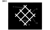
- the mesh-shaped pattern is a negative pattern having a mesh pitch 7 of 150 ⁇ m and a mesh angle 8 of 90°, and having openings 10 with an opening width of 4 ⁇ m and light-shielding portions 9 as shown in FIG. 5.
- development was performed using a 0.1% by mass aqueous solution of tetramethylammonium hydroxide as a developer for a time twice as long as the time required for the exposed portion to dissolve, and then the resultant was rinsed with ultrapure water for 30 seconds, and then heat-cured for 60 minutes in a box oven at 230° C.
- the thickness of the opaque wiring electrode pattern measured by the above-mentioned method was 0.5 ⁇ m.
- the light transmittance of the opaque wiring electrode pattern at a wavelength of 365 nm measured by the above-mentioned method was 0%.
- ⁇ Black photosensitive layer formation process> On the opaque wiring electrode pattern formed in the ⁇ Opaque wiring electrode pattern forming step>, a positive photosensitive resin composition containing the resin and colorant obtained in Production Example 4 was spin-formed to a thickness of 3 ⁇ m after drying. The coating was then dried at 100° C. for 5 minutes to form a black photosensitive layer.
- the black photosensitive layer formed in the ⁇ Black Photosensitive Layer Forming Step> was exposed from the side opposite the opaque wiring electrode formation side using an exposure device (PEM-6M) under the condition of an exposure amount (converted to a wavelength of 365 nm) of 3,000 mJ/ cm2 , and development was performed using a 2.38 mass% tetramethylammonium hydroxide aqueous solution as a developer until the transparent substrate in the exposed area was exposed, forming a blackened layer on the top and sides of the opaque wiring electrode pattern. Further, the substrate was heated in a box oven at 220°C for 60 minutes to obtain a substrate with wiring.
- PEM-6M exposure device
- Example 2 A substrate with wiring was obtained in the same manner as in Example 1, except that in the ⁇ opaque wiring electrode pattern forming step>, the photosensitive conductive paste was applied so that the applied thickness after drying was 2.5 ⁇ m.
- Example 3 A substrate with wires was obtained in the same manner as in Example 1, except that in the ⁇ black photosensitive layer forming step>, the exposure dose was 5,000 mJ/cm 2 and the development time was 1.5 times the time required for the transparent substrate in the exposed area to become exposed.
- Example 4 ⁇ Opaque wiring electrode pattern forming process> A 0.2 ⁇ m thick chromium film was formed as an underlayer (adhesion layer) on one side of a PET film "Lumirror (registered trademark)" T60 (manufactured by Toray Industries, Inc., thickness: 75 ⁇ m, light transmittance at 365 nm wavelength: 77%, light transmittance at 550 nm wavelength: 89%) by sputtering, and then a 2.0 ⁇ m thick copper film was formed over the entire surface by vapor deposition. Next, resist LC-140 (manufactured by Rohm and Haas Electronic Materials Co., Ltd.) was spin-coated on the copper film and dried at 100° C. for 5 minutes.
- resist LC-140 manufactured by Rohm and Haas Electronic Materials Co., Ltd.
- the mesh-shaped pattern is a positive pattern having a mesh pitch 7 of 150 ⁇ m and a mesh angle 8 of 90° as shown in FIG. 6, an opening 10, and a light-shielding portion 9 with a light-shielding width of 16 ⁇ m.
- immersion development was performed for 30 seconds using a 2.38 mass% tetramethylammonium hydroxide aqueous solution as a developer, and further rinsed with ultrapure water for 30 seconds.
- the copper film and the chromium film were etched using a ferric chloride aqueous solution so that the line width was 4.5 ⁇ m, and further rinsed with ultrapure water for 30 seconds.
- immersion development was performed for 4 minutes using a resist stripper JELK-101 (manufactured by Kanto Chemical Co., Ltd.), and further rinsed with ultrapure water for 30 seconds to form an opaque wiring electrode pattern.
- the thickness of the opaque wiring electrode pattern measured by the above-mentioned method was 2.5 ⁇ m.
- the light transmittance at a wavelength of 365 nm of the opaque wiring electrode pattern measured by the above-mentioned method was 0%.
- ⁇ Black photosensitive layer formation process> On the opaque wiring electrode pattern formed in the ⁇ Opaque wiring electrode pattern forming step>, a black photosensitive layer was formed in the same manner as in Example 1.
- a black photosensitive layer was formed and a substrate with wiring was obtained in the same manner as in Example 1, except that the heating temperature of the box oven after the blackening layer was formed was set to 140°C.
- Example 5 A substrate with wiring was obtained in the same manner as in Example 4, except that the chromium film formed as the underlayer in the ⁇ Opaque wiring electrode pattern forming step> was changed to a copper nitride film (black layer).
- Example 1 A substrate with wiring was obtained in the same manner as in Example 1, except that the exposure gap in the ⁇ Opaque wiring electrode pattern forming step> was changed to 0 ⁇ m.
- Example 2 A substrate with wiring was obtained in the same manner as in Example 2, except that the exposure gap in the ⁇ Opaque wiring electrode pattern forming step> was changed to 0 ⁇ m.
- the opaque wiring electrode pattern formed in the ⁇ Opaque wiring electrode pattern forming process> was immersed for 30 seconds in the electrode blackening aqueous solution obtained in Production Example 5, and then washed with water and dried to form a blackened layer on the top and sides of the opaque wiring electrode pattern, thereby obtaining a substrate with wiring.
- Black photosensitive layer formation process A black photosensitive layer was formed in the same manner as in Comparative Example 1.
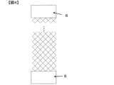
- ⁇ Blackening Layer Forming Step> For the black photosensitive layer formed in the ⁇ Black photosensitive layer forming step>, an exposure mask having a pad portion 6 and a mesh-shaped pattern as shown in FIG. 4 was placed so that the opaque wiring electrode pattern formed in the ⁇ Opaque wiring electrode pattern forming step> and the mask light-shielding portion were overlapped, and an exposure device (PEM-6M; manufactured by Union Optical Co., Ltd.) was used to expose the above-mentioned exposure mask at an exposure dose of 3,000 mJ/cm 2 (converted to a wavelength of 365 nm).
- the mesh-shaped pattern is a positive pattern having a mesh pitch 7 of 150 ⁇ m and a mesh angle 8 of 90° as shown in FIG.
Landscapes
- Engineering & Computer Science (AREA)
- General Engineering & Computer Science (AREA)
- Theoretical Computer Science (AREA)
- Human Computer Interaction (AREA)
- Physics & Mathematics (AREA)
- General Physics & Mathematics (AREA)
- Manufacturing & Machinery (AREA)
- Microelectronics & Electronic Packaging (AREA)
- Shielding Devices Or Components To Electric Or Magnetic Fields (AREA)
Priority Applications (1)
| Application Number | Priority Date | Filing Date | Title |
|---|---|---|---|
| JP2023579679A JPWO2024190033A1 (https=) | 2023-03-10 | 2023-12-22 |
Applications Claiming Priority (2)
| Application Number | Priority Date | Filing Date | Title |
|---|---|---|---|
| JP2023-037300 | 2023-03-10 | ||
| JP2023037300 | 2023-03-10 |
Publications (1)
| Publication Number | Publication Date |
|---|---|
| WO2024190033A1 true WO2024190033A1 (ja) | 2024-09-19 |
Family
ID=92754753
Family Applications (1)
| Application Number | Title | Priority Date | Filing Date |
|---|---|---|---|
| PCT/JP2023/046090 Ceased WO2024190033A1 (ja) | 2023-03-10 | 2023-12-22 | 配線付き基材およびその製造方法 |
Country Status (2)
| Country | Link |
|---|---|
| JP (1) | JPWO2024190033A1 (https=) |
| WO (1) | WO2024190033A1 (https=) |
Citations (5)
| Publication number | Priority date | Publication date | Assignee | Title |
|---|---|---|---|---|
| KR20130086498A (ko) * | 2012-01-25 | 2013-08-02 | (주) 태양기전 | 터치 전극 제조 방법 및 터치 장치 제조 방법 |
| JP2015533682A (ja) * | 2012-08-31 | 2015-11-26 | エルジー・ケム・リミテッド | 伝導性構造体およびその製造方法 |
| WO2016151900A1 (ja) * | 2015-03-20 | 2016-09-29 | 富士フイルム株式会社 | 透明導電フィルム、透明導電フィルムの製造方法およびタッチパネル |
| WO2018168325A1 (ja) * | 2017-03-17 | 2018-09-20 | 東レ株式会社 | 配線電極付き基板の製造方法および配線電極付き基板 |
| CN110673762A (zh) * | 2019-09-29 | 2020-01-10 | 合肥微晶材料科技有限公司 | 一种低可见性触控电极及其制作方法 |
-
2023
- 2023-12-22 WO PCT/JP2023/046090 patent/WO2024190033A1/ja not_active Ceased
- 2023-12-22 JP JP2023579679A patent/JPWO2024190033A1/ja active Pending
Patent Citations (5)
| Publication number | Priority date | Publication date | Assignee | Title |
|---|---|---|---|---|
| KR20130086498A (ko) * | 2012-01-25 | 2013-08-02 | (주) 태양기전 | 터치 전극 제조 방법 및 터치 장치 제조 방법 |
| JP2015533682A (ja) * | 2012-08-31 | 2015-11-26 | エルジー・ケム・リミテッド | 伝導性構造体およびその製造方法 |
| WO2016151900A1 (ja) * | 2015-03-20 | 2016-09-29 | 富士フイルム株式会社 | 透明導電フィルム、透明導電フィルムの製造方法およびタッチパネル |
| WO2018168325A1 (ja) * | 2017-03-17 | 2018-09-20 | 東レ株式会社 | 配線電極付き基板の製造方法および配線電極付き基板 |
| CN110673762A (zh) * | 2019-09-29 | 2020-01-10 | 合肥微晶材料科技有限公司 | 一种低可见性触控电极及其制作方法 |
Also Published As
| Publication number | Publication date |
|---|---|
| JPWO2024190033A1 (https=) | 2024-09-19 |
Similar Documents
| Publication | Publication Date | Title |
|---|---|---|
| CN107109131B (zh) | 触摸面板电极保护膜形成用组合物及其应用 | |
| JP6626238B2 (ja) | 電極フィルムおよびその製造方法 | |
| TWI733001B (zh) | 附有配線電極之基板的製造方法 | |
| JP2014056311A (ja) | 転写材料、静電容量型入力装置の製造方法および静電容量型入力装置、並びに、これを備えた画像表示装置 | |
| JP7081696B2 (ja) | ポジ型感光性樹脂組成物、硬化膜、積層体、導電パターン付き基板、積層体の製造方法、タッチパネル及び有機el表示装置 | |
| CN110476145A (zh) | 触摸传感器及触摸传感器的制造方法 | |
| WO2024190033A1 (ja) | 配線付き基材およびその製造方法 | |
| JP7035437B2 (ja) | 導電パターン付き基板の製造方法および導電パターン付き基板 | |
| JP7472601B2 (ja) | 配線電極付き基板の製造方法 | |
| US12349269B2 (en) | Wiring board | |
| WO2024135082A1 (ja) | 配線基板、遮光層形成用ポジ型感光性樹脂組成物、遮光層転写フィルムおよび配線基板の製造方法 | |
| JP7735896B2 (ja) | 感光性樹脂組成物、配線基板および配線基板の製造方法 | |
| WO2024004318A1 (ja) | 配線電極付き基板の製造方法 | |
| JP2024061122A (ja) | 配線付き基材の製造方法 | |
| JP7322753B2 (ja) | 感光性樹脂組成物、遮光層及びタッチセンサーパネル | |
| WO2020174767A1 (ja) | パターンつき基板の製造方法、回路基板の製造方法、タッチパネルの製造方法、及び積層体 | |
| JPWO2019065234A1 (ja) | 電極付き基板の製造方法 | |
| JP2024128949A (ja) | 透明ヒーター用基材およびそれを用いた透明ヒーター | |
| CN116602061A (zh) | 布线基板 | |
| JP2021152988A (ja) | 導電ペースト、導電パターン形成用フィルム、積層部材及びタッチパネル | |
| JP2005331819A (ja) | 視野制御シート及びその製造方法 | |
| JP6325019B2 (ja) | 転写材料、静電容量型入力装置の製造方法および静電容量型入力装置、並びに、これを備えた画像表示装置 | |
| JPWO2000058788A1 (ja) | 高解像度な光重合性積層体並びにこれを用いた半導体装置 |
Legal Events
| Date | Code | Title | Description |
|---|---|---|---|
| WWE | Wipo information: entry into national phase |
Ref document number: 2023579679 Country of ref document: JP |
|
| 121 | Ep: the epo has been informed by wipo that ep was designated in this application |
Ref document number: 23927635 Country of ref document: EP Kind code of ref document: A1 |
|
| NENP | Non-entry into the national phase |
Ref country code: DE |
|
| 122 | Ep: pct application non-entry in european phase |
Ref document number: 23927635 Country of ref document: EP Kind code of ref document: A1 |