WO2024185001A1 - 可とう導体及び電気機器 - Google Patents
可とう導体及び電気機器 Download PDFInfo
- Publication number
- WO2024185001A1 WO2024185001A1 PCT/JP2023/008277 JP2023008277W WO2024185001A1 WO 2024185001 A1 WO2024185001 A1 WO 2024185001A1 JP 2023008277 W JP2023008277 W JP 2023008277W WO 2024185001 A1 WO2024185001 A1 WO 2024185001A1
- Authority
- WO
- WIPO (PCT)
- Prior art keywords
- flexible conductor
- copper foils
- fastening
- copper foil
- flexible
- Prior art date
- Legal status (The legal status is an assumption and is not a legal conclusion. Google has not performed a legal analysis and makes no representation as to the accuracy of the status listed.)
- Ceased
Links
Images


Classifications
-
- H—ELECTRICITY
- H01—ELECTRIC ELEMENTS
- H01B—CABLES; CONDUCTORS; INSULATORS; SELECTION OF MATERIALS FOR THEIR CONDUCTIVE, INSULATING OR DIELECTRIC PROPERTIES
- H01B5/00—Non-insulated conductors or conductive bodies characterised by their form
- H01B5/02—Single bars, rods, wires, or strips
-
- H—ELECTRICITY
- H01—ELECTRIC ELEMENTS
- H01R—ELECTRICALLY-CONDUCTIVE CONNECTIONS; STRUCTURAL ASSOCIATIONS OF A PLURALITY OF MUTUALLY-INSULATED ELECTRICAL CONNECTING ELEMENTS; COUPLING DEVICES; CURRENT COLLECTORS
- H01R35/00—Flexible or turnable line connectors, i.e. the rotation angle being limited
- H01R35/02—Flexible line connectors without frictional contact members
-
- H—ELECTRICITY
- H01—ELECTRIC ELEMENTS
- H01R—ELECTRICALLY-CONDUCTIVE CONNECTIONS; STRUCTURAL ASSOCIATIONS OF A PLURALITY OF MUTUALLY-INSULATED ELECTRICAL CONNECTING ELEMENTS; COUPLING DEVICES; CURRENT COLLECTORS
- H01R4/00—Electrically-conductive connections between two or more conductive members in direct contact, i.e. touching one another; Means for effecting or maintaining such contact; Electrically-conductive connections having two or more spaced connecting locations for conductors and using contact members penetrating insulation
- H01R4/28—Clamped connections, spring connections
- H01R4/30—Clamped connections, spring connections utilising a screw or nut clamping member
- H01R4/34—Conductive members located under head of screw
Definitions
- the present disclosure relates to ultrasonically bonded flexible conductors and electrical devices including the flexible conductors.
- Prior art discloses a flexible conductor that has a conductive and flexible flexible portion formed by stacking multiple thin copper plates, and terminal portions provided at both ends of the flexible portion, and that in manufacturing this flexible conductor, the thin plates are tin-plated, and the tin plating is melted by resistance welding or the like to join the stacked thin plates (for example, Patent Document 1).
- the present disclosure has been made to solve the problems described above, and aims to provide a flexible conductor in which multiple copper foils are ultrasonically bonded, and an electrical device equipped with the flexible conductor.
- the flexible conductor disclosed herein comprises multiple copper foils stacked in the thickness direction, and the multiple copper foils are ultrasonically bonded to each other at both ends in the extension direction of the copper foil.
- the electrical device includes the above-mentioned flexible conductor, and of the first and second ends of the flexible conductor, a movable part that is fastened to the first end and a terminal to which the second end is fastened.
- the flexible conductor according to the present disclosure can provide a flexible conductor with a low electrical resistance value when current is applied, compared to conventional flexible conductors in which laminated copper foils are joined by tin plating.
- the electrical device according to the present disclosure can provide an electrical device with a low electrical resistance value.
- FIG. 1 is a schematic side view showing a state in which a switch including a flexible conductor according to a first embodiment of the present disclosure is in an open state.
- 1 is a schematic side view showing a state in which a switch including a flexible conductor according to a first embodiment of the present disclosure is closed;
- FIG. 1 is a perspective view of a flexible conductor according to a first embodiment of the present disclosure.
- FIG. 11 is a perspective view of a flexible conductor according to a second embodiment of the present disclosure.
- FIG. 11 is a perspective view of a flexible conductor according to a third embodiment of the present disclosure.
- 6 is a schematic diagram of a flexible conductor according to a third embodiment of the present disclosure, corresponding to a cross section taken along line AA' in FIG. 5.
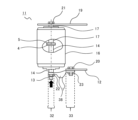
- FIG. 1 is a schematic side view showing a state in which a switch 11 including the flexible conductor 1 in the first embodiment is in an open state, that is, a state in which a movable contact 4 and a fixed contact 5, which will be described later, are not in contact with each other.
- a part of the front surface of the vacuum interrupter 16 is omitted to show the inside of the vacuum interrupter 16.
- the switch 11 includes a flexible conductor 1, a first terminal 12 (a fixed terminal on the flexible conductor side electrically connected to the movable contact 4 via the flexible conductor 1), a driving device tip 13, a first movable part 14 (a movable part connected to the movable contact 4), a vacuum valve 16, a fixed part 17 (a movable part connected to the fixed contact 5), a second terminal 19 (a fixed terminal on the vacuum valve side electrically connected to the fixed contact 5), a bolt 20 and a nut 23 that fix the first terminal 12 and the flexible conductor 1, a bolt 21 that fixes the fixed part 17 and the second terminal 19, and a nut 22 that fixes the first movable part 14, the flexible conductor 1, and the driving device tip 13.
- the switch 11 includes the fixed contact 5 and the fixed part 17 as fixed members, and the movable contact 4 and the first movable part 14 as movable parts.
- the flexible conductor 1 includes a flexible part 38 having electrical conductivity and flexibility, a first end 32, and a second end 33.
- the first end 32 and the second end 33 are located so as to sandwich both ends of the flexible part 38.
- the first end 32 and the second end 33 may be a part on one end side or the other end side of the flexible part 38.
- the first end 32 and the second end 33 of the flexible conductor 1 are not limited to edges, etc., but may be a part excluding the flexible part 38.
- the flexible part 38 is not in the center of the flexible conductor 1 but is located off-center, one end may be the central part of the flexible conductor 1.
- the first end 32 of the flexible conductor 1 is fastened to the driving device tip 13 and the first movable part 14, for example, by a nut 22. That is, the first end 32 of the flexible conductor 1 is connected to the movable part of the switch 11. That is, the first end 32 of the flexible conductor 1 is electrically connected to the first movable part 14.
- the first end 32 of the flexible conductor 1 only needs to be connected to the first movable part 14, and does not have to be connected to the tip 13 of the driving device.
- the drive device tip 13 and the first movable part 14 are fastened together with a nut 22.
- the driving device tip 13 is connected to an external driving device (not shown).
- the driving device is driven, for example, by spring force.
- the driving device includes an insulating rod connected to the first movable part 14.
- the second end 33 of the flexible conductor 1 is fastened to the first terminal 12, for example, by a bolt 20 and a nut 23. That is, the second end 33 of the flexible conductor 1 of the switch 11 is connected to the fixed part of the switch 11. In addition, the second end 33 of the flexible conductor 1 is electrically connected to the first terminal 12.
- first end 32 and the second end 33 that are coupled to the driving device tip 13, the first movable part 14, and the first terminal 12 as the mating members do not refer only to the outer periphery or the end of the flexible conductor 1, and the part that is coupled to the mating member may be located closer to the center than the outer periphery of the flexible conductor 1.
- the fixed portion 17 and the second terminal 19 are fastened with a bolt 21. In addition, the fixed portion 17 and the second terminal 19 are electrically connected.
- FIG. 2 is a schematic side view showing the state in which the switch 11 including the flexible conductor 1 of embodiment 1 is closed, i.e., the state in which the movable contact 4 and the fixed contact 5 are in contact.
- FIG. 2 omits part of the front of the vacuum valve 16 to show the inside of the vacuum valve 16.
- the same reference numerals as in FIG. 1 indicate the same configuration, and therefore explanations are omitted.
- the movable contact 4 and the fixed contact 5 in the vacuum valve 16 are in contact.
- the electrical circuit of the switch 11 is in a closed state.
- the driving device transmits power to the driving device tip 13 to move in the direction of the arrow shown in FIG. 2.
- the driving device tip 13 When power is transmitted to the driving device tip 13, the power is transmitted to the first movable part 14 connected to the driving device tip 13.
- the flexible conductor 1 follows the movement of the first movable part 14 when the switch 11 transitions from an open state to a closed state and from a closed state to an open state.
- the switch 11 to which the flexible conductor 1 of the present invention is applied is not limited to a circuit breaker that uses a vacuum valve, but may be other electrical equipment such as a disconnector in which a fixed part and a movable part are electrically connected.
- the flexible conductor 1 can be easily adapted for use in switches and other electrical equipment having a different configuration from the switch 11 of this embodiment.
- FIG. 3 is a perspective view of the flexible conductor 1 according to embodiment 1.
- the flexible conductor 1 has multiple copper foils 41 stacked in the thickness direction.
- the multiple copper foils 41 are, for example, rectangular with long and short sides.
- the thickness of the copper foils 41 is, for example, about 0.1 mm.
- the flexible conductor 1 also includes ultrasonic joints 34, fastening surfaces 35, and fastening holes 36.
- the ultrasonic joints 34 are located at both ends of the multiple copper foils 41 in the long side direction.
- the outermost copper foil 42 has a fastening surface 35 for fastening to a mating member on a surface different from the laminated surface, i.e., when the multiple copper foils 41 are laminated, the surface different from the laminated surfaces of the two copper foils located on the outermost sides in the lamination direction.
- the fastening surface is referred to as the surface of the surface layer excluding the flexible portion 38, rather than the entire surface of the surface layer of the flexible conductor 1.
- the area where the flexible conductor 1 is fastened to the mating member may be a part of the fastening surface 35, and may be in contact with the first movable portion 14 at the fastening area 37 shown in FIG. 3, for example.
- the ultrasonic joint 34 of the flexible conductor 1 multiple stacked copper foils 41 are ultrasonically joined to each other.
- the ultrasonic joint 34 refers to the portion where multiple stacked copper foils 41 are ultrasonically joined to each other.
- the ultrasonic joints 34 are located on the fastening surface 35 at locations that correspond to the four corners of the copper foil 41.
- the x marks in Figure 3 are processing marks that occur on the conductor surface during ultrasonic bonding.
- the processing marks occur at the position clamped between the horn and anvil of the equipment that performs the ultrasonic bonding.
- Figure 3 shows a case where there are three processing marks at each of the four corners of the copper foil 41 where the ultrasonic bonding portion 34 is located, but the number of processing marks is not limited to three.
- the location of the ultrasonic joints 34 is not limited to the four corners of the copper foil 41, as long as the location does not impair the flexibility of the flexible conductor 1.
- the ultrasonic bonding portion 34 where ultrasonic bonding is performed is not limited to the outer periphery of the flexible conductor 1 as shown in FIG. 4, but may be provided in the center, such as a portion adjacent to the fastening hole 36. It may also be provided in a portion other than the fastening region 37.
- ultrasonic bonding is performed on the ultrasonic bonding portion 34 of the flexible conductor 1, ultrasonic vibrations are applied to the copper foil 41, so that adjacent copper foils 41 are bonded together and integrated.
- the ultrasonic joint 34 of the flexible conductor 1 is joined to integrate the multiple copper foils 41 in the thickness direction, so that when attaching the flexible conductor 1 to the movable part or terminal, the flexible conductor 1 can be easily electrically connected to the drive device tip 13 of the switch 11, the first movable part 14, the first terminal 12, etc., without the copper foils 41 coming apart.
- the copper foils 41 are not joined to each other. Because the copper foils 41 are not joined to each other, the copper foils 41 can bend freely, and the flexible conductor 1 can follow the movement of the first movable part 14.
- the multiple copper foils 41 of the flexible conductor 1 are preferably ultrasonically bonded to one another in the area corresponding to the fastening surface 35. It is also desirable that the ultrasonic bonded portion 34 at least partially overlaps with the area corresponding to the fastening region 37.
- the area corresponding to the fastening surface 35 refers to the area of the copper foil 41 onto which the fastening surface 35 is projected in the thickness direction of the flexible conductor 1.
- the bonding at the ultrasonic bonding portion 34 can suppress contact resistance by pressing the fastening region 37 when attaching the flexible conductor 1 in addition to the bonding by ultrasonic bonding, and can lower the electrical resistance compared to a simple ultrasonic bond.
- Ultrasonic bonding can solid-phase bond the copper foils together.
- the flexible conductor 1 according to this embodiment is bonded by ultrasonic bonding while the copper foils are still in their original state. This means that unlike methods such as spot welding, which melt the tin plating to bond the copper foils, there is no need to plate the copper foils 41 with tin or other metals for bonding.
- the electrical resistance of the flexible conductor 1 can be made lower than that of a flexible conductor connected by conventional plating. Therefore, when creating a flexible conductor with the same resistance, the number of copper foils 41 that form the flexible conductor 1 can be reduced compared to a flexible conductor that uses tin plating.
- each copper foil 41 is not plated, the process of plating the copper foil 41 can be omitted, thereby reducing manufacturing costs.
- the laminated copper foil 41 is ultrasonically bonded without a plated layer, but some layers may be bonded through a plated layer.
- the flexible conductor 1 having the fastening hole 36 makes it easier to use it in switches and other electrical equipment other than the switch 11 of this embodiment, compared to when the flexible conductor 1 does not have the fastening hole 36.
- Fastening holes 36 do not have to be provided.
- the flexible conductor 1 of embodiment 1 i.e., the flexible conductor 1 in which each layer is ultrasonically bonded to each other, the vacuum valve 16, and the switch 11 to which the vacuum valve is attached (excluding the vacuum valve 16, the flexible conductor 1, etc.).
- the ultrasonically bonded flexible conductor 1 can be manufactured by applying ultrasonic vibrations between the copper foils 41 stacked in the thickness direction. The manufacturing method of the flexible conductor 1 will be described in detail later.
- the vacuum valve 16 is attached to the switch 11, and then the flexible conductor 1 is attached to the first movable part 14 (movable electrode rod) connected to the vacuum valve 16.
- the first movable part 14 is attached to the first movable part 14 through the fastening hole 36 of the flexible conductor 1 so that the first movable part 14 passes through the fastening hole 36, and the first movable part 14 and the flexible conductor 1 are joined.
- each copper foil 41 of the flexible conductor 1 is ultrasonically bonded at the ultrasonic bonding part 34, and each copper foil 41 does not come apart, so it can be easily attached to the first movable part 14.
- the first movable part 14 and the flexible conductor 1 can be attached by fastening with a nut.
- the first movable part 14 and the flexible conductor 1 can be attached by other methods such as fitting, without being limited to fastening with a nut.
- the flexible conductor 1 is attached to the first terminal 12.
- the fastening hole of the first terminal 12 is aligned with the fastening hole 36 of the flexible conductor 1, and the flexible conductor 1 is attached by fastening the flexible conductor 1 with a nut 23 through a bolt 20.
- the method of attaching the first movable part 14 and the flexible conductor 1 is not limited to fastening with a bolt, and other methods such as fitting may also be used.
- the order of attachment is not limited to the above, and the order of attachment may be changed as appropriate, for example by previously connecting a part of the flexible conductor 1 before attaching the vacuum valve 16 to the switch 11. Also, while the method of manufacturing the switch 11 having the vacuum valve 16 has been described here, other electrical devices such as disconnectors can be manufactured in a similar manner.
- Embodiment 2 The flexible conductor 2 in the second embodiment will be described with reference to Fig. 4. Description of the same configuration as in the first embodiment will be omitted.
- Fig. 4 the same reference numerals as in Figs. 1 to 3 indicate the same or corresponding parts.
- FIG. 4 is a perspective view of the flexible conductor 2 according to the second embodiment. As shown in FIG. 4, the flexible conductor 2 of this embodiment differs from the flexible conductor 1 of the first embodiment in the position of the ultrasonic joint 34. The following will focus on the differences from the flexible conductor 1 of the first embodiment.
- the ultrasonic joint 34 is located in a range of the fastening surface 35 that includes the fastening hole 36. In other words, the ultrasonic joint 34 is included in the fastening surface 35. Note that the ultrasonic joint 34 and the fastening surface 35 may partially overlap.
- the ultrasonic joint 34 may be provided in a portion adjacent to the fastening hole 36.
- the copper foils 41 in the current path are firmly bonded together.
- the electrical resistance of the flexible conductor 2 can be reduced compared to when the copper foils 41 are fastened with bolts and nuts. Furthermore, if there is no need to reduce the electrical resistance of the flexible conductor 2, the number of copper foils 41 that form the flexible conductor 2 can be reduced.
- the x marks in Figure 4 are processing marks that occur on the conductor surface during ultrasonic bonding. After ultrasonic bonding, processing marks remain on the fastening surface 35 that is fastened to the mating member, but since the processing marks are concave, they do not affect the contact with the mating member.
- the number of processing marks is not limited to the number shown in the figure.
- the arrangement pattern of the processing marks may be, for example, arranged in a grid pattern.
- Embodiment 3 The flexible conductor 3 in the third embodiment will be described with reference to Fig. 5 and Fig. 6. Description of the same configuration as in the first embodiment will be omitted.
- Fig. 5 and Fig. 6 the same reference numerals as in Figs. 1 to 4 indicate the same or corresponding parts.
- FIG. 5 is a perspective view of the flexible conductor 3 according to the third embodiment.
- FIG. 6 is a schematic diagram of the flexible conductor 3 according to the third embodiment, corresponding to a cross section taken along line A-A' in FIG. 5.
- the flexible conductor 3 of this embodiment differs from the flexible conductor 1 of the first embodiment in that a plating layer is provided on the copper foil 42. The following will focus on the differences from the flexible conductor 1 of the first embodiment.
- the flexible conductor 3 in this embodiment is located at the outermost position among the multiple copper foils 41, and the copper foil 42 that is fastened to the mating member has a plating layer of tin or the like on the side that is fastened to the mating member.
- the plating layer may be provided over the entire side of the copper foil 42 that is fastened to the mating member, or, for example, only on the fastening surface 35.
- a plating that melts due to the frictional heat generated by ultrasonic bonding such as tin plating
- the frictional heat generated between the copper foils 41 will cause the plating to melt before bonding is completed in the solid phase, causing slippage between the copper foils. Slippage will prevent the ultrasonic vibrations from being transmitted, resulting in poor bonding.
- a plating layer may be provided on the entirety or part of the copper foil 41 located on the outermost side opposite the copper foil 42 that is fastened to the opposing member, opposite the fastening surface 35 of the copper foil 42.
- plating only to the side of the copper foil 42 that is fastened to the mating member, but a plating layer may be provided on a part of the side of the copper foil 42 that is not fastened to the mating member, or a plating layer may be provided on a part of the other copper foil 41.
- the method for manufacturing a flexible conductor according to embodiments 1 to 3 includes step 101 of stacking multiple copper foils 41 in the thickness direction, and step 102 of ultrasonically joining the multiple stacked copper foils 41 to each other at both ends in the extension direction of the stacked copper foils 41.
- step 102 of ultrasonically bonding the stacked copper foils 41 to each other may include step 102a of ultrasonically bonding the stacked copper foils 41 to each other on the fastening surface 35 of the flexible conductor.
- step 102 of ultrasonically bonding the multiple stacked copper foils 41 to each other may include step 102b of ultrasonically bonding the multiple stacked copper foils 41 to each other at the corners of the stacked copper foils 41.
- the manufacturing method of the flexible conductor according to the first to third embodiments includes step 103 of forming a plating layer on the fastening surface 35 of the copper foil 41, and step 103 of forming the plating layer may be performed before the above step 101, or between the above step 101 and the above steps 102, 102a, and 102b, or even after the above steps 102, 102a, and 102b.
Landscapes
- Pressure Welding/Diffusion-Bonding (AREA)
- Connections By Means Of Piercing Elements, Nuts, Or Screws (AREA)
- Non-Insulated Conductors (AREA)
- Insulated Conductors (AREA)
Priority Applications (4)
| Application Number | Priority Date | Filing Date | Title |
|---|---|---|---|
| PCT/JP2023/008277 WO2024185001A1 (ja) | 2023-03-06 | 2023-03-06 | 可とう導体及び電気機器 |
| KR1020257025386A KR20250130820A (ko) | 2023-03-06 | 2023-03-06 | 가요 도체 및 전기 기기 |
| JP2023571350A JP7460038B1 (ja) | 2023-03-06 | 2023-03-06 | 可とう導体及び電気機器 |
| TW112134504A TWI860840B (zh) | 2023-03-06 | 2023-09-11 | 可撓性導體及電氣機器 |
Applications Claiming Priority (1)
| Application Number | Priority Date | Filing Date | Title |
|---|---|---|---|
| PCT/JP2023/008277 WO2024185001A1 (ja) | 2023-03-06 | 2023-03-06 | 可とう導体及び電気機器 |
Publications (1)
| Publication Number | Publication Date |
|---|---|
| WO2024185001A1 true WO2024185001A1 (ja) | 2024-09-12 |
Family
ID=90474272
Family Applications (1)
| Application Number | Title | Priority Date | Filing Date |
|---|---|---|---|
| PCT/JP2023/008277 Ceased WO2024185001A1 (ja) | 2023-03-06 | 2023-03-06 | 可とう導体及び電気機器 |
Country Status (4)
| Country | Link |
|---|---|
| JP (1) | JP7460038B1 (https=) |
| KR (1) | KR20250130820A (https=) |
| TW (1) | TWI860840B (https=) |
| WO (1) | WO2024185001A1 (https=) |
Citations (4)
| Publication number | Priority date | Publication date | Assignee | Title |
|---|---|---|---|---|
| JPS61176790U (https=) * | 1985-04-24 | 1986-11-04 | ||
| JP3002038U (ja) * | 1994-03-15 | 1994-09-13 | 株式会社井上製作所 | 薄板重ね合せ型の可撓性接続端子 |
| JP2018149557A (ja) * | 2017-03-10 | 2018-09-27 | 住友電装株式会社 | 導電部材の製造装置 |
| JP2021197308A (ja) * | 2020-06-17 | 2021-12-27 | 矢崎総業株式会社 | 導電構造体 |
Family Cites Families (3)
| Publication number | Priority date | Publication date | Assignee | Title |
|---|---|---|---|---|
| US5613751A (en) * | 1995-06-27 | 1997-03-25 | Lumitex, Inc. | Light emitting panel assemblies |
| JP2013131434A (ja) | 2011-12-22 | 2013-07-04 | Tyco Electronics Japan Kk | 可撓導体および可撓導体の製造方法 |
| JP6845974B1 (ja) * | 2019-08-16 | 2021-03-24 | 日東電工株式会社 | カバー部材及びこれを備える部材供給アセンブリ |
-
2023
- 2023-03-06 JP JP2023571350A patent/JP7460038B1/ja active Active
- 2023-03-06 KR KR1020257025386A patent/KR20250130820A/ko active Pending
- 2023-03-06 WO PCT/JP2023/008277 patent/WO2024185001A1/ja not_active Ceased
- 2023-09-11 TW TW112134504A patent/TWI860840B/zh active
Patent Citations (4)
| Publication number | Priority date | Publication date | Assignee | Title |
|---|---|---|---|---|
| JPS61176790U (https=) * | 1985-04-24 | 1986-11-04 | ||
| JP3002038U (ja) * | 1994-03-15 | 1994-09-13 | 株式会社井上製作所 | 薄板重ね合せ型の可撓性接続端子 |
| JP2018149557A (ja) * | 2017-03-10 | 2018-09-27 | 住友電装株式会社 | 導電部材の製造装置 |
| JP2021197308A (ja) * | 2020-06-17 | 2021-12-27 | 矢崎総業株式会社 | 導電構造体 |
Also Published As
| Publication number | Publication date |
|---|---|
| TWI860840B (zh) | 2024-11-01 |
| JPWO2024185001A1 (https=) | 2024-09-12 |
| KR20250130820A (ko) | 2025-09-02 |
| JP7460038B1 (ja) | 2024-04-02 |
| TW202437291A (zh) | 2024-09-16 |
Similar Documents
| Publication | Publication Date | Title |
|---|---|---|
| US4815981A (en) | Flexible printed circuit board terminal structure | |
| KR20210114538A (ko) | 보호 소자 | |
| JP2019046885A (ja) | 半導体装置及びその製造方法 | |
| EP0471508B1 (en) | Power capacitor and method of making the same | |
| JP4942629B2 (ja) | 電力用半導体モジュール | |
| JP3456921B2 (ja) | 金属箔の接合方法並びに超音波溶接具 | |
| WO2024185001A1 (ja) | 可とう導体及び電気機器 | |
| CN100566512C (zh) | 电路基板 | |
| JP2022103052A (ja) | 半導体モジュール、半導体装置および半導体装置の製造方法 | |
| JP2010283014A (ja) | 電力変換装置及びその製造方法 | |
| CN117712196B (zh) | 光伏组件 | |
| JP3568178B2 (ja) | 抵抗溶接装置 | |
| JP3179002B2 (ja) | 導体間の接合方法及び導体間の接合構造 | |
| JPH09320662A (ja) | フレキシブルプリント基板の端子構造及び該端子構造の製造方法 | |
| JP7398050B2 (ja) | ラミネート電池およびその製造方法 | |
| KR102861688B1 (ko) | Empt를 이용한 fpcb와 버스바의 용접 방법 | |
| JP7805838B2 (ja) | スポット溶接方法及びスポット溶接装置 | |
| EP4003632A1 (en) | Power semiconductor module and method of forming the same | |
| WO2021047307A1 (zh) | 一种电机绕组多层导体的点焊方法 | |
| EP4138204B1 (en) | Bus bar | |
| JP7348119B2 (ja) | 溶接方法及び電池モジュールの製造方法 | |
| KR20260061908A (ko) | 알루미늄 라미네이티드 션트 및 그 제조방법 | |
| KR20250145321A (ko) | 이차전지용 전극 및 이를 포함하는 전극 조립체 | |
| JP4724963B2 (ja) | 温度ヒューズ | |
| JP2024168038A (ja) | 電線の端子接合構造及びその製造方法 |
Legal Events
| Date | Code | Title | Description |
|---|---|---|---|
| WWE | Wipo information: entry into national phase |
Ref document number: 2023571350 Country of ref document: JP |
|
| 121 | Ep: the epo has been informed by wipo that ep was designated in this application |
Ref document number: 23926215 Country of ref document: EP Kind code of ref document: A1 |
|
| ENP | Entry into the national phase |
Ref document number: 1020257025386 Country of ref document: KR Free format text: ST27 STATUS EVENT CODE: A-0-1-A10-A15-NAP-PA0105 (AS PROVIDED BY THE NATIONAL OFFICE) |
|
| WWE | Wipo information: entry into national phase |
Ref document number: 202527072936 Country of ref document: IN |
|
| WWP | Wipo information: published in national office |
Ref document number: 202527072936 Country of ref document: IN |
|
| NENP | Non-entry into the national phase |
Ref country code: DE |
|
| 122 | Ep: pct application non-entry in european phase |
Ref document number: 23926215 Country of ref document: EP Kind code of ref document: A1 |