WO2024176357A1 - はんだ材、はんだシートの製造方法および半導体装置の製造方法 - Google Patents
はんだ材、はんだシートの製造方法および半導体装置の製造方法 Download PDFInfo
- Publication number
- WO2024176357A1 WO2024176357A1 PCT/JP2023/006253 JP2023006253W WO2024176357A1 WO 2024176357 A1 WO2024176357 A1 WO 2024176357A1 JP 2023006253 W JP2023006253 W JP 2023006253W WO 2024176357 A1 WO2024176357 A1 WO 2024176357A1
- Authority
- WO
- WIPO (PCT)
- Prior art keywords
- solder
- solder material
- weight
- sheet
- less
- Prior art date
- Legal status (The legal status is an assumption and is not a legal conclusion. Google has not performed a legal analysis and makes no representation as to the accuracy of the status listed.)
- Ceased
Links
Images


Classifications
-
- B—PERFORMING OPERATIONS; TRANSPORTING
- B23—MACHINE TOOLS; METAL-WORKING NOT OTHERWISE PROVIDED FOR
- B23K—SOLDERING OR UNSOLDERING; WELDING; CLADDING OR PLATING BY SOLDERING OR WELDING; CUTTING BY APPLYING HEAT LOCALLY, e.g. FLAME CUTTING; WORKING BY LASER BEAM
- B23K35/00—Rods, electrodes, materials, or media, for use in soldering, welding, or cutting
- B23K35/22—Rods, electrodes, materials, or media, for use in soldering, welding, or cutting characterised by the composition or nature of the material
- B23K35/24—Selection of soldering or welding materials proper
- B23K35/26—Selection of soldering or welding materials proper with the principal constituent melting at less than 400°C
- B23K35/262—Sn as the principal constituent
-
- B—PERFORMING OPERATIONS; TRANSPORTING
- B23—MACHINE TOOLS; METAL-WORKING NOT OTHERWISE PROVIDED FOR
- B23K—SOLDERING OR UNSOLDERING; WELDING; CLADDING OR PLATING BY SOLDERING OR WELDING; CUTTING BY APPLYING HEAT LOCALLY, e.g. FLAME CUTTING; WORKING BY LASER BEAM
- B23K35/00—Rods, electrodes, materials, or media, for use in soldering, welding, or cutting
- B23K35/02—Rods, electrodes, materials, or media, for use in soldering, welding, or cutting characterised by mechanical features, e.g. shape
- B23K35/0222—Rods, electrodes, materials, or media, for use in soldering, welding, or cutting characterised by mechanical features, e.g. shape for use in soldering or brazing
- B23K35/0233—Sheets or foils
-
- C—CHEMISTRY; METALLURGY
- C22—METALLURGY; FERROUS OR NON-FERROUS ALLOYS; TREATMENT OF ALLOYS OR NON-FERROUS METALS
- C22C—ALLOYS
- C22C13/00—Alloys based on tin
Definitions
- This application relates to a solder material, a method for manufacturing a solder sheet, and a method for manufacturing a semiconductor device.
- the melting point of the solder material Sn-3Ag-0.5Cu (values indicate weight percentage, hereafter referred to as SAC305), which is a typical composition of conventional Pb-free solder materials, is 220°C. Therefore, SAC305 softens at temperatures above 175°C and does not provide sufficient bonding strength.
- SAC305 although it is not a solder material, there is a sintered Ag bonding material that uses nano silver particles. However, nano silver particles are expensive and sintered Ag bonding material requires pressure bonding at high pressure, which has significant disadvantages in terms of cost and bonding process.
- Zn-based solder materials have been developed in which part of the main component Sn is replaced with Zn.
- a solder material has been disclosed that, when the total is taken as 100% by weight, consists of 10-70% by weight Sn, 2-10% by weight Al, and the remainder being Zn and unavoidable impurities (see, for example, Patent Document 1).
- Another solder material has been disclosed that, when the total components are taken as 100 mol%, consists of 82-94 mol% Sn, 5-15 mol% Zn, and 1-3 mol% Al. Rewriting the composition of this solder material in weight ratios, it is 2.84-9.09 mol% Zn, 0.23-0.75 mol% Al, and the remainder being Sn (see, for example, Patent Document 2).
- the joining temperature needs to be set to 350 to 410°C.
- the semiconductor element may soften and warp. If the semiconductor element warps, a large residual stress remains at the joint, reducing the joining reliability.
- a copper alloy electrode film, a polyimide insulating film, etc. are formed on the surface of the semiconductor element, the electrical properties of these films may change when heated at 350°C or higher. If the electrical properties of the electrode film, insulating film, etc. change, the characteristics of the semiconductor device change.
- the joining temperature is 250 to 255°C.
- this solder material is about 200°C, it is difficult to apply it to a semiconductor device using a wide band gap semiconductor element that becomes locally or momentarily 180°C or higher during operation. Therefore, it was difficult for conventional Zn-based solder materials to be joined at 250°C or lower and have heat resistance of 180°C or higher.
- This application has been made to solve the above-mentioned problems, and aims to provide a solder material that can be bonded at 250°C or less and has a heat resistance of 180°C or more.
- the solder material of the present application is a solder material whose main components are Sn, Zn, and Al, and has two endothermic peaks in differential scanning calorimetry, and is a mixture of a first alloy phase having an endothermic peak between 190°C and 230°C, and a second alloy phase having an endothermic peak between 240°C and 380°C.
- the solder material of the present application has two endothermic peaks in differential scanning calorimetry, and is a mixture of a first alloy phase having an endothermic peak between 190°C and 230°C, and a second alloy phase having an endothermic peak between 240°C and 380°C, making it possible to bond at 250°C or less and to have heat resistance of 180°C or more.
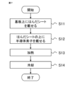
- FIG. 4 is a flowchart of a manufacturing process of the solder sheet according to the first embodiment.
- 5A to 5C are schematic diagrams illustrating a process for producing a solder sheet according to the first embodiment.
- 5A to 5C are schematic diagrams illustrating a process for producing a solder sheet according to the first embodiment.
- 5A to 5C are schematic diagrams illustrating a process for producing a solder sheet according to the first embodiment.
- 1 is a schematic cross-sectional view of a solder material according to a first embodiment.
- FIG. 4 is a diagram showing the results of differential scanning calorimetry of the solder material according to the first embodiment.
- 1 is a flowchart of a manufacturing process of a semiconductor device according to a first embodiment.
- FIG. 4 is a schematic diagram of a die shear strength test in the first embodiment.
- 1 is a table showing the composition of the solder material and the test results of the joint strength in the first embodiment.
- Embodiment 1. 1 is a flow chart of a manufacturing process of a solder sheet according to the first embodiment.
- step S01 raw powders of solder material are mixed. Specifically, 10 g of Zn powder, 5 g of Al powder, and 85 g of Sn powder are mixed.
- the average particle size of the raw powder is preferably 10 to 100 ⁇ m.
- the average particle size of the raw powder is the average particle size measured using, for example, a laser diffraction type particle size distribution analyzer.
- step S02 the mixed raw material powders are melted in a melting furnace to produce molten solder.
- the melting temperature is set to 700°C.
- the melting temperature is equal to or higher than the melting point of Al, which has the highest melting point among the raw material powders Zn (melting point 420°C), Al (melting point 660°C), and Sn (melting point 232°C), the powders can melt and be mixed uniformly.
- step S03 the molten solder is dropped onto a flat stage.
- step S04 the molten solder dropped onto the stage is formed into a sheet with a squeegee before it solidifies.
- FIG. 2 is a schematic diagram showing the state in which molten solder 1 is dropped onto a flat stage 2 in step S03.
- Stage 2 is, for example, a flat plate made of stainless steel and has a temperature adjustment function.
- the temperature of stage 2 when molten solder 1 is dropped in step S03 is set to approximately 300° C.
- the thickness of molten solder 1 when dropped onto stage 2 is non-uniform.
- FIGS. 3 and 4 are schematic diagrams showing the state when the molten solder 1 is formed into a sheet by the squeegee 3 in step S04.
- the distance between the squeegee 3 and the stage 2 is set to, for example, 100 ⁇ m, which is the thickness of the solder sheet.
- the squeegee 3 moves parallel to the surface of the stage 2. At this time, the distance between the squeegee 3 and the stage 2 is always kept constant.
- the squeegee 3 is moved to form the molten solder 1 into a sheet to produce the solder sheet 4.
- step S05 the solder sheet 4 formed into a sheet shape is cooled.
- the atmosphere in steps S03 to S05 may be an oxidizing atmosphere such as air, an inert atmosphere such as nitrogen or argon, or a reducing atmosphere such as formic acid or hydrogen.
- the temperature of stage 2 is adjusted to cool from 300°C to 100°C in a cooling time of more than 20 seconds and not more than 200 seconds.
- the cooling rate at this time is, in absolute value, 1°C/sec or more and less than 10°C/sec.
- the solder sheet 4 formed in this manner is cut to a predetermined size. For example, it is cut to a 5 mm square to match the bonding surface of the semiconductor element.
- the thickness of the solder sheet 4 is preferably 0.05 mm or more and less than 1 mm. The thickness of the solder sheet 4 can be adjusted by the distance between the squeegee 3 and the stage 2.
- steps S01 and S02 Zn powder, Al powder, and Sn powder are mixed and melted at the same time, but other methods may be used.
- Zn powder and Sn powder may be mixed and melted to first produce a bulk body of Sn and Zn, and then the bulk body may be melted again and Al powder may be added.
- steps S03 and S04 molten solder is dropped and formed into a sheet before it solidifies, but other methods may be used. For example, the molten solder is first made into small ball-shaped solids. Then, the small ball-shaped solids are distributed on a stage.
- the ball-shaped solids distributed on the stage may be heated and compressed at 700°C to be formed into a sheet.
- the solder sheet formed into a sheet by heating and compressing at 700°C is cooled from 300°C to 100°C in a cooling time of more than 20 seconds but not more than 200 seconds.
- the cooling rate at this time expressed in absolute value, is greater than or equal to 1°C/sec and less than 10°C/sec.
- FIG. 5 is a schematic cross-sectional view of the solder material constituting the solder sheet of this embodiment.
- FIG. 5 is a schematic diagram of the composition when the cross-section of the solder material is observed under magnification with a scanning electron microscope.
- the solder material 14 constituting the solder sheet 4 of this embodiment is separated into two phases.
- the second alloy phase 12 is dispersed within the first alloy phase 11. If the cross-sectional shape of the second alloy phase 12 is approximated as a circle, its diameter is 20 ⁇ m or less.
- FIG. 6 shows the results of differential scanning calorimetry of the solder material according to this embodiment.
- Differential scanning calorimetry (hereinafter referred to as DSC) is a method of measuring the temperature difference between a reference material and a material to be measured while applying a certain amount of heat, and measuring the endothermic reaction and exothermic reaction of the material to be measured from the temperature difference.
- the horizontal axis is temperature
- the vertical axis is the amount of heat (hereinafter referred to as DSC value) calculated from the temperature difference between the reference material and the material to be measured.
- the vertical axis is shown in logarithm.
- the direction in which the DSC value decreases is an endothermic reaction
- the direction in which the DSC value increases is an exothermic reaction.
- two endothermic peaks are observed in the DSC curve of the solder material according to this embodiment.
- the two endothermic peaks are endothermic peak A that appears at about 210°C and endothermic peak B that appears at about 340°C.
- first and second alloy phases shown in Figure 5 and the two endothermic peaks shown in Figure 6.
- the endothermic reaction in the first alloy phase 11 corresponds to endothermic peak A
- the endothermic reaction in the second alloy phase 12 corresponds to endothermic peak B.
- the first alloy phase 11 is a phase containing Sn as the main component and Al and Zn therein
- the second alloy phase 12 is a phase containing Zn as the main component and Al and Sn therein.
- the specific heat capacities of the first and second alloy phases were compared.
- the specific heat capacities of the first and second alloy phases were measured in accordance with Japanese Industrial Standard JIS K 7123, which allows specific heat capacity to be calculated using DSC. As a result, it was found that the specific heat capacity of the first alloy phase was greater than that of the second alloy phase.
- Specific heat capacity is the amount of heat required to raise the temperature of a unit mass of a substance by a unit amount, and its unit is J/(kg ⁇ K).
- the solder material When manufacturing a solder material such as SAC305, which is an alloy of Sn, Ag, and Cu, the solder material is generally rapidly cooled so as not to cause phase separation.
- the absolute value of the cooling rate of the molten solder material is, for example, 50°C/sec or more.
- the absolute value of the cooling rate from 300°C to 100°C is set to 1°C/sec or more and less than 10°C/sec, so that a solder material separated into two phases, a first alloy phase and a second alloy phase, is obtained, as shown in Figure 5.
- Fig. 7 is a flow chart of the manufacturing process of the semiconductor device according to this embodiment.
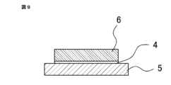
- step S11 the solder sheet 4 is placed on the substrate 5, which is the member to be joined.
- Fig. 8 is a schematic diagram showing the state in which the solder sheet 4 is placed on the substrate 5 in step S11.
- the substrate 5 is, for example, a copper plate such as tough pitch copper, having a thickness of 1 mm and a size of 10 mm square.
- the solder sheet 4 is, for example, 100 ⁇ m thick and 5 mm square.
- the outermost surface of the substrate 5 is solid copper and is not plated. However, the outermost surface of the substrate 5 may be coated with an anti-rust agent with a decomposition temperature of 100°C or less, as long as it does not affect the solder joint. Also, to prevent the solder sheet 4 from shifting when it is placed on the substrate 5, the surface of the substrate 5 may be coated with an adhesive that thermally decomposes at 100°C or more. The viscosity of the adhesive is preferably 200 Pa ⁇ s or more. Alternatively, a resist film may be applied to the surface of the substrate 5 in areas other than the joining surface, to prevent the solder sheet 4 from shifting when it is placed on the substrate 5.
- the solder sheet 4 may be slightly curved. This is because the solder sheet 4 melts when heated, so the initial shape has little effect. However, if the solder sheet 4 is curved to the extent that it causes the semiconductor element to shift position when it is placed on the sheet in the next process, the curvature of the solder sheet 4 must be corrected.
- FIG. 9 is a schematic diagram showing the state in which the semiconductor element 6 is placed on the solder sheet 4 in step S12.
- the semiconductor element 6 is, for example, a semiconductor element using SiC, and is 100 ⁇ m thick and 5 mm square.
- a Ni film may be formed on the joining surface of the semiconductor element 6 facing the solder sheet 4 to improve wettability with the solder material.
- an adhesive may be applied to the joining surface of either the semiconductor element 6 or the solder sheet 4 to prevent the semiconductor element 6 from shifting when placed on it.
- the substrate 5, solder sheet 4, and semiconductor element 6 are placed on a hot plate 7 and placed in an airtight furnace 8.
- the inside of the airtight furnace 8 is adjusted to an atmosphere of 3 volume % hydrogen, which can reduce oxide films, with the remainder being nitrogen.
- the solder sheet 4 is heated to 250°C for 10 minutes using the hot plate 7 to melt it. In this way, the substrate 5 and semiconductor element 6 are bonded with the solder material 14.
- the semiconductor device 13 in which the substrate 5 and the semiconductor element 6 are joined with the solder material 14 is transferred to the cooling stage 9 in the sealed furnace 8.
- the inside of the sealed furnace 8 is adjusted to an atmosphere of 3 volume % hydrogen capable of reducing oxide films, with the remainder being nitrogen.
- the solder material 14 is cooled from 250°C to 100°C over 500 seconds using the cooling stage 9.
- the absolute value of the cooling rate at this time is 0.3°C/sec. In the manufacturing process of general-purpose semiconductor devices, such a slow cooling rate is not adopted. This is because the tact time becomes long.
- step S14 by adopting a cooling rate (absolute value) of 0.3°C/sec, it is possible to suppress the occurrence of warping, undulation, etc. of the semiconductor element 6 caused by the thermal contraction of the solder material 14.
- a temperature adjustment stage having both the functions of a hot plate and a cooling stage may be used.
- This temperature adjustment stage can adjust the temperature of the material on the stage within a temperature range of, for example, 20°C to 400°C. By using such a temperature adjustment stage, the process of transferring the semiconductor device 13 from the hot plate 7 to the cooling stage 9 is not required.
- the cooling time from 250°C to 100°C is preferably 300 seconds or more.
- the cooling rate from 250°C to 100°C is preferably 0.5°C/second or less in absolute value. If the cooling time from 250°C to 100°C is 300 seconds or more, it is possible to suppress the occurrence of warping, undulation, etc. of the semiconductor element 6 caused by thermal contraction of the solder material 14.
- the solder material 14 that joins the substrate 5 and the semiconductor element 6 can be joined at temperatures below 250°C and has a heat resistance of 180°C or higher. The reasons for this are explained below.
- the solder material of this embodiment has two alloy phases: a first alloy phase corresponding to endothermic peak A appearing at about 210°C, and a second alloy phase corresponding to endothermic peak B appearing at about 340°C.
- the first alloy phase having an endothermic peak at about 210°C melts and can bond the substrate and the semiconductor element.
- the semiconductor device is heated to 180°C or higher, the first alloy phase having an endothermic peak at about 210°C softens, but the second alloy phase having an endothermic peak at about 340°C does not soften.
- the solder material of the semiconductor device of this embodiment does not soften more than necessary even at 180°C or higher, and has heat resistance of 180°C or higher.
- the composition of the solder material is 10% by weight Zn, 5% by weight Al, and 85% by weight Sn. From here on, the characteristics of solder material with a different composition ratio will be explained. Note that the solder material of this embodiment may contain unavoidable impurities other than the main components.
- step S01 of the solder sheet manufacturing process flowchart shown in Figure 1 multiple types of solder sheets were manufactured by changing the mixing ratio of Zn powder, Al powder, and Sn powder when mixing the raw solder powder. Using these solder sheets, multiple semiconductor devices with different solder composition were manufactured based on the semiconductor device manufacturing process flowchart shown in Figure 7. A die shear strength test was performed on multiple semiconductor devices manufactured in this way.
- FIG. 12 is a schematic diagram of a die shear strength test in this embodiment.
- a die 10 is brought into contact with the side of a semiconductor element 6 of a semiconductor device 13 in which a substrate 5 and a semiconductor element 6 are joined with a solder material 14, and a load is applied to the die 10 in a direction parallel to the joining surface.
- the load applied to the die 10 is gradually increased, and the value of the load at which the semiconductor element 6 cannot withstand the load from the die 10 and moves laterally is defined as the joining strength of the joining surface.
- the joining strength of the semiconductor device 13 was measured at 20°C.
- FIG. 13 is a table showing the composition of the solder material and the test results of the joint strength in this embodiment.
- the vertical rows show the weight percentage of Zn in the solder material
- the horizontal columns show the weight percentage of Al in the solder material.
- the weight percentage of Sn in the solder material is calculated by subtracting the weight percentage of Zn and the weight percentage of Al from 100 weight percent.
- " ⁇ " and " ⁇ " indicate the evaluation results of the joint strength.
- the minimum joint strength was set to 40 MPa, and if the joint strength at 20°C was 40 MPa or more, it was defined as " ⁇ ", and if the joint strength at 20°C was less than 40 MPa, it was defined as " ⁇ ".
- the reason for setting the minimum joint strength at 40 MPa is that the joint strength at 20°C of SAC305, a general-purpose solder material, is about 40 MPa.
- solder materials with less than 5% Zn by weight the ratio of Sn in the solder material is high, and the strength of the solder material itself is low.
- the joint strength at 20°C is less than 40 MPa.
- solder materials with 20% or more Zn by weight the strength of the solder material itself is high, but the ratio of Sn in the solder material is low.
- the solder material does not melt completely at the joining temperature of 250°C, and the initial joint strength is low.
- the joint strength at 20°C is less than 40 MPa.
- the ratio of Zn increases, the solder material is more susceptible to oxidation, and it is thought that the initial joint strength is reduced due to the effects of oxidation.
- the joint strength at 20°C is less than 40 MPa.
- the strength of the solder material itself is high, but the ratio of Sn in the solder material is low. Therefore, at a joining temperature of 250°C, the solder material does not melt completely, and the initial joint strength is reduced. As a result, the joint strength is less than 40 MPa. Note that when the ratio of Al is high, the joint strength can be improved by setting the joining temperature to 250°C or higher. However, setting the joining temperature to 250°C or higher is not preferable because it may cause warping of the semiconductor element.
- solder material that has two endothermic peaks in DSC measurement, and that is a mixture of a first alloy phase having an endothermic peak from 190°C to 230°C and a second alloy phase having an endothermic peak from 240°C to 380°C, can be bonded at 250°C or less and has heat resistance of 180°C or more.
- the height of the endothermic peak on the low temperature side is lower.
- the peak temperatures of the two endothermic peaks shift to the high temperature side as the proportion of Al increases. Therefore, it is estimated that when the Al content is 10% or more by weight, the solder material becomes difficult to melt at a joining temperature of 250°C.
- the atmosphere during bonding and cooling is 3% hydrogen by volume with the remainder being nitrogen, but if there are no safety issues, it may be 100% hydrogen by volume.
- the atmosphere may be an organic acid such as formic acid.
- organic acids that can be used include formic acid, acetic acid, lauric acid, caprylic acid, pelargonic acid, heptyl acid, and caproic acid.
- the solder sheet may be immersed in an organic acid before being introduced into the manufacturing process of the semiconductor device, and a coating of an organic acid salt may be formed on the surface of the solder sheet.
- solder material 1 molten solder, 2 stage, 3 squeegee, 4 solder sheet, 5 substrate, 6 semiconductor element, 7 hot plate, 8 sealed furnace, 9 cooling stage, 10 die, 11 first alloy phase, 12 second alloy phase, 13 semiconductor device, 14 solder material.
Landscapes
- Engineering & Computer Science (AREA)
- Mechanical Engineering (AREA)
- Chemical & Material Sciences (AREA)
- Materials Engineering (AREA)
- Metallurgy (AREA)
- Organic Chemistry (AREA)
- Die Bonding (AREA)
Priority Applications (4)
| Application Number | Priority Date | Filing Date | Title |
|---|---|---|---|
| PCT/JP2023/006253 WO2024176357A1 (ja) | 2023-02-21 | 2023-02-21 | はんだ材、はんだシートの製造方法および半導体装置の製造方法 |
| JP2025501983A JPWO2024176357A1 (https=) | 2023-02-21 | 2023-02-21 | |
| DE112023005851.2T DE112023005851T5 (de) | 2023-02-21 | 2023-02-21 | Lötmaterial, verfahren zur herstellung einer lötfolie und verfahren zur herstellung eines halbleiterbauelemnents |
| CN202380093613.1A CN120712154A (zh) | 2023-02-21 | 2023-02-21 | 焊料、焊料片的制造方法及半导体装置的制造方法 |
Applications Claiming Priority (1)
| Application Number | Priority Date | Filing Date | Title |
|---|---|---|---|
| PCT/JP2023/006253 WO2024176357A1 (ja) | 2023-02-21 | 2023-02-21 | はんだ材、はんだシートの製造方法および半導体装置の製造方法 |
Publications (1)
| Publication Number | Publication Date |
|---|---|
| WO2024176357A1 true WO2024176357A1 (ja) | 2024-08-29 |
Family
ID=92500382
Family Applications (1)
| Application Number | Title | Priority Date | Filing Date |
|---|---|---|---|
| PCT/JP2023/006253 Ceased WO2024176357A1 (ja) | 2023-02-21 | 2023-02-21 | はんだ材、はんだシートの製造方法および半導体装置の製造方法 |
Country Status (4)
| Country | Link |
|---|---|
| JP (1) | JPWO2024176357A1 (https=) |
| CN (1) | CN120712154A (https=) |
| DE (1) | DE112023005851T5 (https=) |
| WO (1) | WO2024176357A1 (https=) |
Citations (6)
| Publication number | Priority date | Publication date | Assignee | Title |
|---|---|---|---|---|
| JPH08273987A (ja) * | 1995-03-31 | 1996-10-18 | Nitsuko Corp | アルミ固体コンデンサ |
| JP2002301588A (ja) * | 2000-12-21 | 2002-10-15 | Hitachi Ltd | はんだ箔および半導体装置および電子装置 |
| JP2007275921A (ja) * | 2006-04-05 | 2007-10-25 | Mitsubishi Electric Corp | はんだ合金およびはんだ付方法 |
| JP2011251298A (ja) * | 2010-05-31 | 2011-12-15 | Sumitomo Metal Mining Co Ltd | Znを主成分とするPbフリーはんだ合金 |
| WO2014024715A1 (ja) * | 2012-08-10 | 2014-02-13 | 千住金属工業株式会社 | 高温鉛フリーはんだ合金 |
| JP2018107126A (ja) * | 2016-12-22 | 2018-07-05 | 三ツ星ベルト株式会社 | 導電性ペースト並びに電子基板及びその製造方法 |
-
2023
- 2023-02-21 WO PCT/JP2023/006253 patent/WO2024176357A1/ja not_active Ceased
- 2023-02-21 JP JP2025501983A patent/JPWO2024176357A1/ja active Pending
- 2023-02-21 DE DE112023005851.2T patent/DE112023005851T5/de active Pending
- 2023-02-21 CN CN202380093613.1A patent/CN120712154A/zh active Pending
Patent Citations (6)
| Publication number | Priority date | Publication date | Assignee | Title |
|---|---|---|---|---|
| JPH08273987A (ja) * | 1995-03-31 | 1996-10-18 | Nitsuko Corp | アルミ固体コンデンサ |
| JP2002301588A (ja) * | 2000-12-21 | 2002-10-15 | Hitachi Ltd | はんだ箔および半導体装置および電子装置 |
| JP2007275921A (ja) * | 2006-04-05 | 2007-10-25 | Mitsubishi Electric Corp | はんだ合金およびはんだ付方法 |
| JP2011251298A (ja) * | 2010-05-31 | 2011-12-15 | Sumitomo Metal Mining Co Ltd | Znを主成分とするPbフリーはんだ合金 |
| WO2014024715A1 (ja) * | 2012-08-10 | 2014-02-13 | 千住金属工業株式会社 | 高温鉛フリーはんだ合金 |
| JP2018107126A (ja) * | 2016-12-22 | 2018-07-05 | 三ツ星ベルト株式会社 | 導電性ペースト並びに電子基板及びその製造方法 |
Also Published As
| Publication number | Publication date |
|---|---|
| DE112023005851T5 (de) | 2025-12-04 |
| JPWO2024176357A1 (https=) | 2024-08-29 |
| CN120712154A (zh) | 2025-09-26 |
Similar Documents
| Publication | Publication Date | Title |
|---|---|---|
| US8920580B2 (en) | Solder paste and electronic device | |
| CN102892549B (zh) | 混合合金焊料膏 | |
| US20120055586A1 (en) | Variable melting point solders | |
| CN115139009B (zh) | 预成型焊料及其制备方法、以及焊接接头的制备方法 | |
| JPS59124150A (ja) | 接合方法 | |
| US11628519B2 (en) | Solder joint | |
| KR20140050728A (ko) | 무연 솔더 조성물 | |
| TWI304006B (en) | Tin/indium lead-free solders for low stress chip attachment | |
| JP2018079480A (ja) | 低温用のBi−In−Sn系はんだ合金、それを用いた電子部品実装基板及びその実装基板を搭載した装置 | |
| Sharma et al. | Epoxy polymer solder pastes for micro-electronic packaging applications | |
| JP4560830B2 (ja) | はんだペースト用Au−Sn合金粉末 | |
| JP4136844B2 (ja) | 電子部品の実装方法 | |
| TW202138576A (zh) | 無鉛且無銻之焊料合金、焊球,及焊料接頭 | |
| JP2011062736A (ja) | 鉛フリー高温用接合材料 | |
| WO2024176357A1 (ja) | はんだ材、はんだシートの製造方法および半導体装置の製造方法 | |
| CN1977368B (zh) | 软钎焊方法、芯片焊接用软钎料颗粒、芯片焊接软钎料颗粒的制造方法及电子零件 | |
| JP5147349B2 (ja) | バンプ形成用ペースト、及びバンプ構造体 | |
| WO2018207177A1 (en) | Method and kit for attaching metallic surfaces | |
| JP5646230B2 (ja) | 鉛フリー接合材料およびその製造方法 | |
| JP2010062256A (ja) | バンプ付き半導体チップの製造方法 | |
| JPWO2009034628A1 (ja) | はんだプリコート基板、実装基板およびはんだプリコート方法 | |
| TW201706421A (zh) | Au-Sn-Ag系焊膏以及使用此Au-Sn-Ag系焊膏接合或密封之電子元件 | |
| JP2021175578A (ja) | 成形はんだ及び成形はんだの製造方法 | |
| WO2024122217A1 (ja) | 接合構造体及び該接合構造体の接合部を形成するための接合材料 | |
| JP2015188892A (ja) | ボール状Au−Sn−Ag系はんだ合金並びにこのボール状Au−Sn−Ag系はんだ合金を用いて封止された電子部品及び電子部品搭載装置 |
Legal Events
| Date | Code | Title | Description |
|---|---|---|---|
| 121 | Ep: the epo has been informed by wipo that ep was designated in this application |
Ref document number: 23924011 Country of ref document: EP Kind code of ref document: A1 |
|
| WWE | Wipo information: entry into national phase |
Ref document number: 2025501983 Country of ref document: JP |
|
| WWE | Wipo information: entry into national phase |
Ref document number: 112023005851 Country of ref document: DE |
|
| WWP | Wipo information: published in national office |
Ref document number: 112023005851 Country of ref document: DE |
|
| 122 | Ep: pct application non-entry in european phase |
Ref document number: 23924011 Country of ref document: EP Kind code of ref document: A1 |